Introduction to Organic Thin Film Transistors and Design of n … · Introduction to Organic Thin...
16
Introduction to Organic Thin Film Transistors and Design of n-Channel Organic Semiconductors Christopher R. Newman, ‡ C. Daniel Frisbie,* ,‡ Demetrio A. da Silva Filho, § Jean-Luc Bre ´das, § Paul C. Ewbank, † and Kent R. Mann † Departments of Chemistry and of Chemical Engineering and Materials Science, University of Minnesota, Minneapolis, Minnesota 55455, and School of Chemistry and Biochemistry, Georgia Institute of Technology, Atlanta, Georgia 30332 Received April 14, 2004. Revised Manuscript Received June 23, 2004 The development of new organic semiconductors with improved performance in organic thin film transistors (OTFTs) is a major challenge for materials chemists. There is a particular need to develop air-stable n-channel (electron-conducting) organic semiconductors with performance comparable to that of p-channel (hole-conducting) materials, for organic electronics to realize the benefits of complementary circuit design, i.e., the ability to switch transistors with either positive or negative gate voltages. There have been significant advancements in the past five years. In terms of standard OTFT metrics such as the field effect mobility (μ FET ) and on-to-off current ratio (I ON /I OFF ), n-channel OTFTs have achieved performance comparable both to that of n-channel amorphous silicon TFTs and to that of the best reported p-channel (hole-conducting) OTFTs; however, issues of device stability linger. This review provides a detailed introduction to OTFTs, summarizes recent progress in the development of new n-channel organic semiconductors, and discusses the critical properties that any prospective n-channel material must have. Methods important to semiconductor design such as electronic structure calculations and synthetic structural modifications are highlighted in a case study of the development of a new n-channel material based on a terthiophene modified with electron-withdrawing groups. The review concludes with a discussion of directions for future work in this area. 1. Introduction Over the past 10 years there has been remarkable progress in the development of thin film transistors (TFTs) based on organic semiconductors. In terms of the key figures of merit, namely, the on-to-off current ratio (I ON /I OFF ), the field effect mobility (μ FET ), and the threshold voltage (V T ), the performance of the best organic TFTs now rivals that of commercial amorphous silicon TFTs, which are commonly employed as the pixel switching elements in active matrix flat panel displays. An important advantage of organic semiconductors vis- a ` -vis amorphous silicon is that they can be deposited onto substrates at low temperatures, meaning they are compatible with flexible plastic substrates. 1,2 A number of industrial laboratories are working hard to develop low-cost, large-area plastic electronics employing tran- sistors and diodes based on organic semiconductors. The good performance of organic TFTs (OTFTs) makes it more likely that these efforts will succeed. As noted by Dimitrakopoulos and Malenfant in their 2002 review, 3 industrial emphasis is shifting away from organic semiconductor testing and more toward manufacturing process development. From a materials science perspective, there remain a number of important unanswered questions concern- ing the performance of organic semiconductors in OT- FTs. 4 For example, transistors based on polycrystalline films of pentacene, a fused ring oligomer, set the benchmark for OTFT performance, routinely displaying values of μ FET in excess of 1 cm 2 V -1 s -1 , I ON /I OFF > 10 8 , and V T near 0 V. 5 It is not perfectly clear how these impressive electrical characteristics depend in detail on the crystal structure and morphology of pentacene films; TFTs based on polycrystalline films of many other organic semiconductors do not have comparable trans- port characteristics. Indeed, it is reasonable to ask why pentacene TFTs appear so far to be unique in their combination of exceptional transport properties. Basic understanding of structure-property relationships is essential for answering this question and a host of others including the following: How high can carrier mobilities be in films of crystalline organic semiconduc- tors? Can good mobilities be obtained in solution- processable films that are only partially crystalline? What are the structural and electronic factors that facilitate or impede transport in organic semiconductor films? Are there particular molecular structures and crystal packing motifs that are especially favorable for transport? What is the role of grain boundaries? These unanswered questions reflect a significant gap in basic knowledge of structure-property relationships on all length scales in organic semiconductors. Perhaps the most significant point is that this knowledge gap * To whom correspondence should be addressed at the Department of Chemical Engineering and Materials Science, University of Min- nesota. E-mail: [email protected]. † Department of Chemistry, University of Minnesota. ‡ Department of Chemical Engineering and Materials Science, University of Minnesota. § Georgia Institute of Technology. 4436 Chem. Mater. 2004, 16, 4436-4451 10.1021/cm049391x CCC: $27.50 © 2004 American Chemical Society Published on Web 08/31/2004
Transcript of Introduction to Organic Thin Film Transistors and Design of n … · Introduction to Organic Thin...

Introduction to Organic Thin Film Transistors andDesign of n-Channel Organic Semiconductors
Christopher R. Newman,‡ C. Daniel Frisbie,*,‡ Demetrio A. da Silva Filho,§Jean-Luc Bredas,§ Paul C. Ewbank,† and Kent R. Mann†
Departments of Chemistry and of Chemical Engineering and Materials Science,University of Minnesota, Minneapolis, Minnesota 55455, and School of Chemistry and
Biochemistry, Georgia Institute of Technology, Atlanta, Georgia 30332
Received April 14, 2004. Revised Manuscript Received June 23, 2004
The development of new organic semiconductors with improved performance in organicthin film transistors (OTFTs) is a major challenge for materials chemists. There is aparticular need to develop air-stable n-channel (electron-conducting) organic semiconductorswith performance comparable to that of p-channel (hole-conducting) materials, for organicelectronics to realize the benefits of complementary circuit design, i.e., the ability to switchtransistors with either positive or negative gate voltages. There have been significantadvancements in the past five years. In terms of standard OTFT metrics such as the fieldeffect mobility (µFET) and on-to-off current ratio (ION/IOFF), n-channel OTFTs have achievedperformance comparable both to that of n-channel amorphous silicon TFTs and to that ofthe best reported p-channel (hole-conducting) OTFTs; however, issues of device stabilitylinger. This review provides a detailed introduction to OTFTs, summarizes recent progressin the development of new n-channel organic semiconductors, and discusses the criticalproperties that any prospective n-channel material must have. Methods important tosemiconductor design such as electronic structure calculations and synthetic structuralmodifications are highlighted in a case study of the development of a new n-channel materialbased on a terthiophene modified with electron-withdrawing groups. The review concludeswith a discussion of directions for future work in this area.
1. Introduction
Over the past 10 years there has been remarkableprogress in the development of thin film transistors(TFTs) based on organic semiconductors. In terms of thekey figures of merit, namely, the on-to-off current ratio(ION/IOFF), the field effect mobility (µFET), and thethreshold voltage (VT), the performance of the bestorganic TFTs now rivals that of commercial amorphoussilicon TFTs, which are commonly employed as the pixelswitching elements in active matrix flat panel displays.An important advantage of organic semiconductors vis-a-vis amorphous silicon is that they can be depositedonto substrates at low temperatures, meaning they arecompatible with flexible plastic substrates.1,2 A numberof industrial laboratories are working hard to developlow-cost, large-area plastic electronics employing tran-sistors and diodes based on organic semiconductors. Thegood performance of organic TFTs (OTFTs) makes itmore likely that these efforts will succeed. As noted byDimitrakopoulos and Malenfant in their 2002 review,3industrial emphasis is shifting away from organicsemiconductor testing and more toward manufacturingprocess development.
From a materials science perspective, there remaina number of important unanswered questions concern-ing the performance of organic semiconductors in OT-FTs.4 For example, transistors based on polycrystallinefilms of pentacene, a fused ring oligomer, set thebenchmark for OTFT performance, routinely displayingvalues of µFET in excess of 1 cm2 V-1 s-1, ION/IOFF > 108,and VT near 0 V.5 It is not perfectly clear how theseimpressive electrical characteristics depend in detail onthe crystal structure and morphology of pentacene films;TFTs based on polycrystalline films of many otherorganic semiconductors do not have comparable trans-port characteristics. Indeed, it is reasonable to ask whypentacene TFTs appear so far to be unique in theircombination of exceptional transport properties. Basicunderstanding of structure-property relationships isessential for answering this question and a host ofothers including the following: How high can carriermobilities be in films of crystalline organic semiconduc-tors? Can good mobilities be obtained in solution-processable films that are only partially crystalline?What are the structural and electronic factors thatfacilitate or impede transport in organic semiconductorfilms? Are there particular molecular structures andcrystal packing motifs that are especially favorable fortransport? What is the role of grain boundaries? Theseunanswered questions reflect a significant gap in basicknowledge of structure-property relationships on alllength scales in organic semiconductors. Perhaps themost significant point is that this knowledge gap
* To whom correspondence should be addressed at the Departmentof Chemical Engineering and Materials Science, University of Min-nesota. E-mail: [email protected].
† Department of Chemistry, University of Minnesota.‡ Department of Chemical Engineering and Materials Science,
University of Minnesota.§ Georgia Institute of Technology.
4436 Chem. Mater. 2004, 16, 4436-4451
10.1021/cm049391x CCC: $27.50 © 2004 American Chemical SocietyPublished on Web 08/31/2004

impedes rational efforts to design organic semiconduc-tors with further enhancements in electrical perfor-mance.
A particular design need is in the area of n-channel(also commonly referred to as “n-type”) organic semi-conductors. As described in the next section, TFTs basedon n-channel semiconductors conduct electrons andachieve their high conductivity “on” state with positivegate voltages, whereas most OTFTs (e.g., pentaceneTFTs) are p-channel devices (i.e., they conduct holes)and turn on with negative gate voltages. The motivationfor seeking good n-channel OTFTs is that they enablecomplementary circuit design. Electrical engineers areproficient at developing low-power complementary cir-cuits that utilize both positive and negative gate volt-ages to turn transistors on and off. The lower powerrequirement of complementary circuits is an attractivefeature for many potential applications for plasticelectronics, such as radio frequency identification (RFID6)tags, in which the organic circuit must be energized bya local radio frequency (rf) field. Consequently, thedevelopment of good n-channel OTFTs with perfor-mance comparable to that of pentacene TFTs is a majorgoal for organic electronics.
Historically there have been more examples of goodp-channel materials than n-channel materials for OTFTs.In the past five years there has been increased attentionto n-channel materials, but early efforts can be tracedback to the mid-1990s. Very recently, electron mobilitiesnear 1 cm2 V-1 s-1 have been achieved in several organicsemiconductors, which is on par with hole mobilities inpentacene films. However, there is currently no n-channel analogue for pentacene, i.e., an n-channelorganic semiconductor that is clearly superior to allothers in terms of overall performance. This situationmay change soon given the intense research in this field,and progress on the vexing issue of air stability to bediscussed later.
In this paper we review recent progress in the designof good n-channel semiconductors for OTFTs and specifythe key requirements that these materials must satisfyto be practical. Our review complements the previouslymentioned review by Dimitrakopoulos and Malenfant,who summarized p-channel and n-channel OTFT de-velopment efforts up to the summer of 2001. Specifically,we include developments that have occurred in the pasttwo and a half years (e.g., more new n-channel materi-als, higher reported mobilities, and the observation ofambipolar (electron and hole) transport), and we alsopresent a case study that summarizes our experiencesin trying to develop a successful n-channel material,which we think is illustrative of the challenges andopportunities that researchers face in this area. Animportant theme that we emphasize is the role thatelectronic structure calculations can play in identifyingand designing promising n-channel semiconductor can-didates.
2. OTFT Geometry and Operation
Parts a and b of Figure 1 show cross-sections of top-contact and bottom-contact transistor geometries thatare most commonly used for OTFTs. In both cases, anorganic semiconductor film is deposited on a gate/insulator substrate and is contacted with metallic source
and drain electrodes. In the top-contact case, Figure 1a,the organic film is deposited first, followed by the metalelectrodes. In the bottom-contact case, Figure 1b, thisdeposition sequence is reversed. Usually, the gate/insulator assembly consists of a metal or doped semi-conductor gate electrode coated with an insulating oxide(typically 200-400 nm thick), though polymeric insula-tors are also used and might ultimately be preferablefor flexible electronics. The organic semiconductor film(!30-50 nm thick) can be deposited from the vaporphase or coated from solution. If desired, surface treat-ments on the insulator may be used prior to depositionof the semiconductor layer. These treatments have beenobserved to have profound effects on the resulting thinfilm structure and electrical characteristics.7,8 The metalsource and drain electrodes are often vapor-depositedthrough a shadow mask, but conductive inks that canbe printed are also employed. Source-drain channellengths, L, shown in Figure 1c, typically range from 10to 100 µm, and channel widths, W, are usually between100 µm and 1 mm.
The voltage applied between the source and drain isreferred to as the source-drain voltage, VD. For a givenVD, the amount of current that flows through thesemiconductor film from source to drain is a strongfunction of the voltage, VG, applied to the gate electrode.The semiconductor film and the gate electrode arecapacitively coupled such that application of a bias onthe gate induces charge in the semiconductor film, asshown schematically in Figure 1c. Much of this chargeis mobile and moves in response to the applied source-drain voltage VD. Ideally, when no gate voltage isapplied, the conductance of the semiconductor film isextremely low because there are no mobile chargecarriers; i.e., the device is “off”. When the gate voltageis applied, mobile charges are induced, and the transis-tor is on.
The origin of the gate-induced charging (also knownas the “field effect”) is clarified in the simplified elec-tronic energy level diagrams shown in Figure 2. Figure2a shows the positions of the highest occupied molecularorbitals (HOMOs) and lowest unoccupied molecularorbitals (LUMOs) of the organic semiconductor relativeto the Fermi levels of the source and drain contacts. Inthis case, the gate bias is zero. If a small source-drainbias were applied, there would be no conduction becausethere are no mobile charges in the semiconductor. Partsb and d of Figure 2 show the situation when a positivegate voltage is applied with VD ) 0 and VD > 0,
Figure 1. Schematic of top (a) and bottom (b) contact organicTFTs. (c) Relevant voltages and geometry for a TFT.
Reviews Chem. Mater., Vol. 16, No. 23, 2004 4437
respectively. Application of a positive gate voltageproduces a large electric field at the organic/insulatorinterface. This field causes the HOMO and LUMO levelsin the semiconductor to shift down (lower in energy)with respect to the Fermi levels of the metal contacts,which remain fixed as their potentials are externallycontrolled. If the gate field is large enough, the LUMOwill become resonant with the Fermi levels of thecontacts, and electrons can then flow from the contactsinto the LUMO, Figure 2b. Now there are mobileelectrons at the semiconductor/insulator interface, whichupon application of a drain voltage, Figure 2d, resultin electric current between the source and drain. Thissame reasoning applies with negative gate bias, Figure2c,e. Negative gate bias causes the HOMO and LUMOlevels to shift up such that the HOMO becomes resonantwith the contact Fermi levels and electrons spill out ofthe semiconductor and into the contacts, leaving posi-tively charged holes. These holes are now the mobilecharges that move in response to an applied drainvoltage, Figure 2e. Note that in Figure 2d,e the sourceelectrode is always the charge-injecting contact regard-less of the sign of the gate voltage.
The diagrams in Figure 2 are a useful way to visualizethe mechanism by which conduction in OTFTs ismodulated by the gate electrode. However, this descrip-tion is simplistic, and a quantitative description of theprocess must account for the presence of charge trapsand residual dopants, for example. In addition, thediagrams in Figure 2 might lead one to believe that anyorganic semiconductor can be made to conduct holes orelectrons, depending on the sign of the gate voltage. This
is not true; in general, a given organic semiconductorcan be made more conductive with either a positive ora negative gate voltage, but not both, with only a fewrecent exceptions. Hence, organic semiconductors areclassified according to whether they are hole (p-channel)conductors or electron (n-channel) conductors.
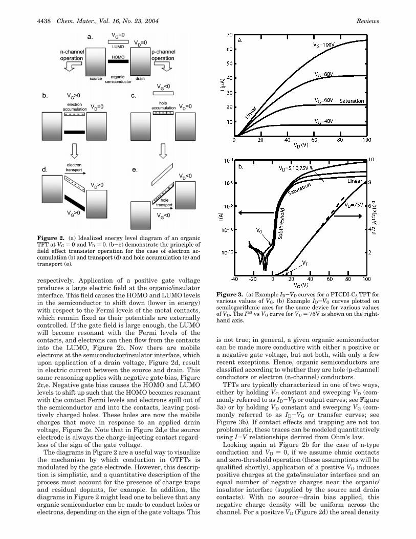
TFTs are typically characterized in one of two ways,either by holding VG constant and sweeping VD (com-monly referred to as ID-VD or output curves; see Figure3a) or by holding VD constant and sweeping VG (com-monly referred to as ID-VG or transfer curves; seeFigure 3b). If contact effects and trapping are not tooproblematic, these traces can be modeled quantitativelyusing I-V relationships derived from Ohm’s law.
Looking again at Figure 2b for the case of n-typeconduction and VD ) 0, if we assume ohmic contactsand zero-threshold operation (these assumptions will bequalified shortly), application of a positive VG inducespositive charges at the gate/insulator interface and anequal number of negative charges near the organic/insulator interface (supplied by the source and draincontacts). With no source-drain bias applied, thisnegative charge density will be uniform across thechannel. For a positive VD (Figure 2d) the areal density
Figure 2. (a) Idealized energy level diagram of an organicTFT at VG ) 0 and VD ) 0. (b-e) demonstrate the principle offield effect transistor operation for the case of electron ac-cumulation (b) and transport (d) and hole accumulation (c) andtransport (e).
Figure 3. (a) Example ID-VD curves for a PTCDI-C8 TFT forvarious values of VG. (b) Example ID-VG curves plotted onsemilogarithmic axes for the same device for various valuesof VD. The I1/2 vs VG curve for VD ) 75V is shown on the right-hand axis.
4438 Chem. Mater., Vol. 16, No. 23, 2004 Reviews

of charge (C/cm2) induced at a given position x alongthe channel is proportional to the voltage differenceVG - V(x):
where Cox is the capacitance of the insulator per unitarea, typically reported in nF/cm2, n(x) is the numberdensity of charges in the channel (no./cm3), e is thefundamental unit of charge, and t is the thickness ofthe charged layer in the channel.
More often than not, the point at which mobile chargecarriers are first introduced into the organic film doesnot correspond to VG ) 0. For an n-channel semiconduc-tor, a mismatch between the Fermi level of the metaland the organic LUMO (analogous to the conductionband for conventional semiconductors) results in chargetransfer between the metal and organic, causing a dipoleand band bending in the organic. This necessitates theapplication of a nonzero VG (often referred to as VFB inthe literature) just to achieve the flat-band condition.Furthermore, if there are large numbers of deep electrontraps present in the film (deep enough to render theelectrons trapped in them effectively immobile), thesewill have to be filled before the channel can conduct.Conversely, if the channel is inadvertently doped withnegative carriers (e.g., by remnant impurities), it willbe conductive at VG ) 0.
To handle these various situations, it is convenientto define a threshold gate voltage, VT, necessary toinduce mobile charges. VT is a parameter that lumps
together all the effects described in the precedingparagraph. For an n-channel material, doping thechannel shifts VT negatively (in other words, the devicehas to be biased negatively to shut it off), deep trapsshift VT positively, and mismatch between the LUMOand metal Fermi level can shift it in either directiondepending on the nature of the misalignment. Includingthe threshold voltage, eq 1 becomes
Figure 4a shows that, when VD ) 0, the channelcharge density is uniform for a given VG (since ideallyVT is not a function of x, and when VD ) 0, V(x) ) 0).However, when VD is nonzero but less than VG, there isa linear gradient in the charge concentration, Figure4b. For a given small value of VD, the average value ofqind is Cox(VG - VT - VD/2), which is the induced arealcharge density in the center of the channel. To the leftof center, the charge density will be higher, and to theright, the charge density will be lower.
Now we arrive at the I-V relationship for a TFT in asimplistic fashion; a more rigorous derivation can befound in standard texts.9 To begin, we simply writedown Ohm’s law and use the definition of conductivity:
where ! is the conductivity, µ is the carrier mobility (i.e.,velocity per unit electric field), and nind,av is the averagecarrier concentration in the channel. Substituting eq 2into eq 3, we obtain
which is commonly rewritten as
Equation 5 is the standard “linear regime” equation, andit describes transport for the case shown pictorially inFigure 4b, where VD < (VG - VT). Equation 4 is easierto understand in that the terms inside the bracketsmultiplied by Cox give the average areal charge densityin the channel; the higher the average charge density,the higher the drain current will be. Equation 5 showsthat in the so-called linear regime the current scaleslinearly with the gate voltage and quadratically withthe drain voltage. For (VG - VT) . VD it is ap-proximately correct to drop the VD/2 term.
For the purposes of calculating the field effect mobilityin the linear region, it is useful to define two deriva-tives:
when (VG - VT) . VD.
Figure 4. (a) Carrier concentration profile of TFT in the linearregime. (b) Pinch-off occurs when VD " VG - VT. (c) Carrierconcentration profile of TFT in the saturation regime.
qind(x) ) n(x) et ) Cox(VG - V(x)) (1)
qind(x) ) n(x) et ) Cox(VG - VT - V(x)) (2)
ID
tW ) !VD
L w ID ) WL (nind,avet) µVD (3)
ID ) WL Cox µ [(VG - VT) -
VD
2 ]VD (4)
ID ) WL Cox µ [(VG - VT)VD -
VD2
2 ] (5)
gm )!ID
!VG
|||VD
) WL Cox µlinVD
gd )!ID
!VD
|||VG
! WL Cox µlin(VG - VT) (6)
Reviews Chem. Mater., Vol. 16, No. 23, 2004 4439

These derivatives are referred to as the transconduc-tance (gm) and conductance (gd), respectively. The mobil-ity can be calculated from either of these derivativesfor a given VD or VG, or a composite linear regionmobility can be calculated from the variation of gm withVD or gd with VG:
Following one of the high-VG traces in Figure 3a, forVG - VT . VD, the channel has a nearly uniform carrierconcentration from source to drain (Figure 4a), and thecurrent is approximately linear with VD in this region.As VD is increased, the carrier concentration profilebecomes increasingly nonuniform, decreasing from thesource to the drain electrode and resulting in quadraticI-V characteristics. When VD ) VG - VT (Figure 4b),the channel becomes “pinched”. In other words, thereis no longer a potential difference between the gate andthe part of the channel nearest the drain electrode,resulting in a region near the drain completely depletedof free carriers. Further increases in VD serve only topush this pinch point slightly backward toward thesource electrode (this effect has been exaggerated inFigure 4c). As long as the device length L is much longerthan the width of this depletion region, further increasesin VD yield no additional current, since the integratedresistance of the channel from the source to the pinchpoint remains the same, and carriers are swept acrossthe narrow space charge region from the pinch point tothe drain by the (comparatively) high electric field inthe depletion region. Substituting VD ) VG - VT intoeq 5 yields the equation describing the I-V character-istics of a field effect transistor in saturation:
Therefore, the device mobility can also be calculatedin the saturation region from the slope of a line drawnthrough the linear part of an ID,sat
1/2 vs VG plot. This isshown in Figure 3b along with the I-V characteristicson semi-logarithmic axes. A few things should be notedregarding analysis of the saturation characteristics.First, the mobilities calculated in the linear and satura-tion regions do not always agree; often µsat is higher.Since the integrated resistance of the channel is higherin saturation than in the linear region, contact resis-tances are likely to be less noticeable in this region.Ohmic contacts were assumed in deriving eq 4, butnonnegligible voltage drops near the contacts due toSchottky barriers and (in the case of top-contact devices)access resistances through the ungated portion of theorganic semiconductor are almost invariably present inthese devices.10 Second, the threshold voltage VT canbe calculated from the intercept of a line drawn throughthe linear region of the ID,sat
1/2 vs VG plot. This is shownin Figure 3b. Here, and in most devices, one notices thatthis intercept does not always coincide with the expo-nential increase in current (designated V0) shown on theadjacent logarithmic axes. In addition to deep traps thatimmobilize carriers at least as long as the measurementduration, there is inevitably also a distribution ofshallower traps with release rates on the order of the
measurement time. As VG is increased, more of thesetraps are filled and unavailable to trap subsequentcarriers. As a consequence, the mobility in the satura-tion region appears to be a continuously increasingfunction of VG, and this results in an offset between V0and VT (and thus renders VT little more than a fitparameter for these devices). In general, the higher themobility of the device, the smaller this offset is, sincelow mobilities and large offsets are both symptomaticof high shallow-trap concentrations.
In addition to µ and VT (or V0), two other metrics areoften cited in evaluating TFT performance. The first isthe on/off current ratio, ION/IOFF, which is self-explana-tory and is typically reported as 10x. Achieving a highon/off ratio generally translates to maximizing themobility, which more or less determines ION, andminimizing the off current (due to dopants). The secondis the subthreshold swing, S:
S is a measure of how rapidly the device switches fromthe off state to the on state in the region of exponentialcurrent increase and is typically reported in V decade-1
or mV decade-1. A more useful metric for comparisonbetween films deposited on different dielectrics or ondielectrics of varying thickness is the normalized sub-threshold swing, Sn ) CoxS (V nF cm-2 decade-1), whichyields the required number of gate-induced carriers toeffect a one-decade increase in the current near V0 andthus allows meaningful comparison of films on differentdielectrics. A large subthreshold swing generally impliesa large concentration of shallow traps, i.e., a diffuseturn-on region. Both ION/IOFF and Sn are dependent onthe device geometry, operating conditions, and mea-surement apparatus (current detection levels in par-ticular), and thus are only truly useful when cited alongwith this information or when used to compare devicestested under identical circumstances.
3. Literature Summary of n-Channel OrganicMaterials for Transistors
There are several reasons why development of high-performance n-channel organic TFT materials haslagged behind that of p-channel materials. The first isthat the metals typically used for making contact tothese materials (Au, Ag, and other noble metals prima-rily) have work functions better suited for injection ofholes into the HOMO than of electrons into the LUMOfor typical organic semiconductors. Low-work-functionmetals such as Al, Mg, or Ca, while expected to havelower electron injection barriers, oxidize easily andreadily form reactive complexes with the organic semi-conductor.11 Second, unsubstituted oligothiophenes andoligoacenes have relatively small electron affinities(!2.8 eV for pentacene in the solid state12). Usually,these molecules have to be augmented with electron-withdrawing side groups to stabilize the anionic formsof the molecule and allow them to efficiently transportnegative charges. Even if the molecule can be chemicallytailored to exhibit n-channel conduction, the susceptibil-ity of organic anions to atmospheric oxidants such asO2 and H2O remains a problem.13 Electronically, this
dgm
dVD)
dgd
dVG) W
L Cox µlin (7)
ID,sat )W2L Cox µsat(VG - VT)2 (8)
S )dVG
d(log ID)(9)
4440 Chem. Mater., Vol. 16, No. 23, 2004 Reviews

susceptibility may manifest itself in the formation ofefficient electron traps or the sharp degradation oftransport properties upon exposure to air. Therefore, thearea of n-channel organic semiconductors involves notonly maximizing the mobility of these materials but alsominimizing the deterioration of electronic propertiesover time.
Dimitrakopoulos and Malenfant have summarized theprogress in the area of molecular n-channel organicsemiconductors for thin film applications from the firstwork using metal-phthalocyanines in 1990 to the achieve-ment of electron mobilities of !0.6 cm2 V-1 s-1 in 2001.3The purpose of this section is to summarize the pro-gress that has been made since then in small-moleculen-channel organic semiconductors, to summarize thework in n-channel polymeric semiconductors (an areain which considerably less work has been done), and todiscuss potentially useful n-channel materials whichhave not yet been fully tested as the active layer inTFTs.
Figure 5 shows the molecular structures of n-channelorganic semiconductors that have been characterized in
a TFT configuration, both molecular and polymeric,most of which are constructed via the addition ofelectron-withdrawing groups (cyano, perfluoroalkyl, etc.)to known p-type cores (naphthalene, perylene, 6T, etc.).Many have been discussed in ref 3 and will only bebriefly revisited here. Early work with the rare-earth-metal/organic complexes Pc2Lu and Pc2Tm yieldeddevices with mobilities of !10-4 cm2 V-1 s-1, and in thecase of Pc2Lu, ambipolar (electron and hole) transportwas observed after annealing.14 TCNQ and TCNNQ,both of which have received considerable attention asthe acceptor half of organic/metal complexes, yieldedelectron mobilities of !10-5 and 10-3 cm2 V-1 s-1,respectively, in single-component thin films.15,16 All ofthese mobilities were measured under vacuum, and inall cases the electrical properties were reported todegrade quickly when the complexes were exposed toair. In the case of Pc2Lu, n-channel conduction wascompletely suppressed upon breaking of the vacuum.In 1998, Bao et al. demonstrated that the addition ofstrong electron-withdrawing groups to metallophthalo-cyanines could result in air-stable n-channel organic
Figure 5. Structures of n-channel semiconductors with known TFT characteristics.
Reviews Chem. Mater., Vol. 16, No. 23, 2004 4441

semiconductors. A mobility of 0.03 cm2 V-1 s-1 in airwas reported for the perfluorinated F16CuPc.17
As of 2000, the highest reported electron field effectmobility in an organic thin film was for C60 on an amine-modified surface18 (µ " 0.3 cm2 V-1 s-1), but theperformance of these films degraded rapidly uponexposure to air. Recently, Kobayashi et al. reportedmobilities as high as 0.56 cm2 V-1 s-1 for C60 filmsfabricated by molecular beam deposition, but thesemobilities could only be achieved by performing devicefabrication and electrical characterization without break-ing the vacuum.19
Oligothiophenes constitute one of the most extensivelycharacterized series of p-channel molecules,20,21 but anumber of groups have demonstrated that the oligo-thiophene backbone can be used as a foundation forbuilding n-channel organic semiconductors. Facchetti etal. have synthesized a series of n-channel semiconduc-tors by adding perfluorohexyl groups (C6F13) to the R,"(DFH-nT) or #,#′ (isoDFH-nT) positions of oligothio-phenes, where n ) 0, 0.5, 1, 1.5, or 2. The highestobserved mobility in these materials is !0.05 cm2 V-1
s-1 for thermally evaporated DFH-4T films.22-25 Thissame group has also synthesized n-channel semiconduc-tors based on permutations of thiophene and fluoroarenegroups. Electron mobilities as high as 0.08 cm2 V-1 s-1
have been observed in FTTTTF.26 All of these mobilitieswere measured in vacuum.
Chesterfield et al. have recently reported on theelectrical characterization of the n-channel organicsemiconductor DCMT, a quinoid terthiophene derivativewith electron-withdrawing dicyanomethylene groups.Mobilities as high as 0.2 cm2 V-1 s-1 were observedunder vacuum in the best films of DCMT.27,28 Thesehigh-mobility films showed only n-channel behavior, butother films of this same material exhibited both p- andn-channel behavior,28 although the mobility for bothcarrier types in these films was significantly lower.Ambipolar device operation has also been achieved intwo-component solution-cast organic TFTs. The n-chan-nel material in these films (with µ " 0.02) was the C60derivative PCBM.29 This same material has also beensolution-cast in single-component n-channel TFTs withmobilities as high as 5 # 10-3 cm2 V-1 s-1.30
The most extensive work thus far on n-channelmolecular organic semiconductors has involved com-pounds formed by adding electron-withdrawing dian-hydride or diimide moieties to naphthalene and perylenecores (NTCDI-R and PTCDI-R in Figure 5). The earliestattempts to fabricate TFTs from these materials yieldedmobilities of !10-3 and 10-4 cm2 V-1 s-1 for NTCDAand NTCDI,16 respectively, and !10-4 cm2 V-1 s-1 forthin films of PTCDA.31 Later, Katz et al. demonstratedthat the mobility and air stability of these devices couldbe greatly improved by incorporating various N,N′substituents on NTCDI. In particular, it was found thatfluorinated side groups (R ) CH2C6H4CF3 in this case),which may act as a kinetic barrier to the diffusion ofoxidizing species, yield devices with mobilities >0.1 cm2
V-1 s-1 in air.32 In 2001, Malenfant et al. demonstratedmobilities of 0.6 in PTCDI-C8 in a vacuum, but thethreshold voltage in this device was !75 V, indicatinga large concentration of traps.33 Recently, Chesterfieldet al. have demonstrated saturation mobilities as high
as 1.7 cm2 V-1 s-1 in the same molecule, and withthreshold voltages of 10-15 V.34 Chesterfield et al.investigated the effect of the alkyl chain length (C5, C8,and C12)34 on device characteristics and the effect ofvarious metals on contact resistance and device perfor-mance of thin films of the C5 derivative.10
The literature on n-channel semiconducting polymersfor TFT applications is significantly sparser than foroligomeric materials. Most of the work on semiconduct-ing polymer TFTs has focused on p-channel materialssuch as regioregular poly(3-hexylthiophene) (P3HT), forwhich mobilities as high as 0.1 cm2 V-1 s-1 have beenobserved. To the best of our knowledge, the work ofBabel and Jenehke on the polymers BBL and BBBrepresents the only available information on intrinsicn-channel conduction in polymer TFTs.35,36 An electronmobility of !0.1 cm2 V-1 s-1 was observed in a solution-cast film of BBL in air, but only 10-6 cm2 V-1 s-1 wasobserved for similarly fabricated BBB films.
In addition to compounds with known transistorproperties, there are a number of relatively new molec-ular and polymeric materials whose potential as n-channel semiconductors has been gauged by theirstructural similarity to known n-channel organics,37
their electrochemical and spectroscopic properties,38-46
and their electrical performance in alternative devicestructures such as Schottky diodes or organic light-emitting diodes (OLEDs).39,40,42,43,47 Figure 6 shows ahandful of these structures. DB-TCV3T, the aromaticanalogue of the quinoid DCMT, exhibits a field effectmobility of !0.02 cm2 V-1 s-1, while PTCDI-PPEEB,which shows liquid crystalline behavior, exhibits mobili-ties of !0.05 cm2 V-1 s-1 in preliminary thin film work.48
Electron mobilities as high as 0.6 cm2 V-1 s-1 have beenobserved in DFHCO-4T recently, and ambipolar trans-port (with n- and p-channel mobilities of !10-3) hasbeen observed in thin films of DHCO-4T.49
4. Materials Requirements for n-ChannelOrganic Semiconductors
In this section, we discuss the properties that organicsemiconductors must have to function as good n-channelmaterials in OTFTs. At the outset of this discussion, itis worth making the point that the transport mechanismin OTFTs is not clear. There are essentially two limitingcase models, (1) carrier hopping and (2) multiple trap-ping and release (MTR),50 and the list of materialsrequirements for n-channel conduction depends some-what on which mechanism is operating. Nevertheless,there are important characteristics that are clearlynecessary no matter which transport model is correct.On the basis of this and the experiences of researchersin this area, it is possible to assemble lists of bothnecessary and desirable properties.
4.1. Necessary Properties. 4.1.1. Conjugated $-Elec-tron System with High Electron Affinity (>3.0 eV). Allorganic semiconductors are made from molecules thatare highly conjugated and rich in $-electrons; there areseveral reasons for this. The first reason is that the$-orbitals are energetically accessible for electricaltransport. For example, for typical p-channel materials,the ionization potentials associated with electrons in theHOMO are about 5 eV, far smaller than the 10 eVionization energies common to alkanes. Practically
4442 Chem. Mater., Vol. 16, No. 23, 2004 Reviews

speaking, this means it is possible to inject positivecharge (holes) from metal electrodes (particularly high-work-function metals) into films of conjugated p-channelmolecules. A second reason is that, once a charge isplaced on a conjugated molecule, it is rapidly delocalizedover the $-orbital system. This of course leads toextremely fast conduction within the molecule, but moreimportantly, the delocalization also facilitates transportof charge between molecules (intermolecular chargetransfer) by maximizing the spatial overlap of thedelocalized charge with the electronic states on anadjacent molecule.
For n-channel materials, it is the electron affinity, notthe ionization potential, which must be high enough toallow efficient injection of electrons into the emptyLUMO of the semiconductor molecules. It appears thatfrom a practical standpoint the electron affinity needsto be at least 3.0 eV, but should not be much greaterthan 4.0 eV. The reason for the upper limit, which isdifficult to achieve anyway, is that if the molecule istoo electrophilic its stability in ambient conditions willbe overly compromised. For example, films of electro-philic molecules can “air-dope” by reaction with atmo-
spheric moisture, and such doping is not desirable forOTFT performance.
4.1.2. Good Intermolecular Electronic Overlap. Forintermolecular charge transport to be fast, overlapbetween wave functions on adjacent molecules must beas large as possible. This is naturally a function of thetype of bonding between the semiconductor molecules,but it also depends on the size of the molecules, themolecular symmetry, and the symmetry of the crystalpacking.51 The critical role of electronic overlap and itsdependence on the packing geometry is discussed indetail in section 5, so we will not discuss it further here.However, it is important to note that in many crystallineorganic semiconductor materials there are two majorcontributions to intermolecular bonding, the dispersionand the quadrupolar interactions. The role of dispersiveinteractions is generally well recognized, and conse-quently, some workers refer to crystalline organicsemiconductors as “van der Waals” solids, though thisis often an inaccurate characterization. In contrast, theimportance of the quadrupolar interaction is frequentlyneglected in the organic electronics literature. Thequadrupolar interaction arises from the charge polar-
Figure 6. Structures of n-channel semiconductors with unknown or unpublished TFT characteristics.
Reviews Chem. Mater., Vol. 16, No. 23, 2004 4443

ization present within many rigid aromatic systems.Benzene (C6H6), for example, has a quadrupole moment(think of two back-to-back dipoles) stemming from thecombination of the net negative charge in the $-cloudsabove and below the plane of the molecule and the netpositive charge from the exposed protons on the periph-ery of the benzene ring. In the solid state, benzene packs“edge-to-face” such that a proton on one ring interactsstrongly with the $-system on an adjacent ring. In thiscase, the quadrupolar interaction completely dominatesthe interaction energy. On the other hand, the crystalstructure of pentacene, an archetypal p-channel organicsemiconductor, results from the interplay of strongdispersive interactions between the delocalized $-orbit-als, which favor face-to-face $-stacking, and the quadru-polar interaction, which favors edge-to-face packing.Determining how these two different types of intermo-lecular interactions affect intermolecular orbital overlapis an important area of research.52,53
4.1.3. Good Film-Forming Properties. Efficient trans-port of charge through a semiconductor film requiresthat the film be continuous and ordered. In the case ofvapor-deposited, low-molecular-weight organic semi-conductors that form polycrystalline films, it is neces-sary that there be good connectivity between the grains.It is also important that the polycrystalline film behighly oriented so that the fast transport directions inthe grains lie parallel to the dielectric surface; highlyoriented polycrystalline films display higher carriermobilities than amorphous films or randomly orientedcrystalline films.3 In the case of solution-processed films(small molecules or polymers), comparable crystallinityis not achieved, meaning there are amorphous domainswith presumably lower carrier mobilities.54 Chain ori-entation is certainly possible in the case of polymers andis desirable for transport. The quality of solution-castfilms depends strongly on the solubility of semiconduct-ing molecules in a given solvent, and this continues topose challenges for solution processing, as discussedfurther below.
4.1.4. Chemical Purity. Chemical impurities in organicsemiconductors for OTFT applications are undesirablefor two reasons. First, impurities can result in charge-trapping sites in organic semiconductor films, whichlowers the average mobility and degrades the OTFT oncurrent and threshold (onset) voltage stability. Second,impurities can function as dopants, thereby increasingthe conductivity of the film in the off or ungated state,which results in large leak currents, excessive powerdissipation, and low on-to-off current ratios. Thus, it isimportant to work with organic semiconductors that areas pure as possible, and this remains a major challengefor organic electronics because of the complexity of thesynthetic processes used to make the materials and thelarge number of different types of impurities that canbe present.
4.1.5. Stability. Stability refers to the time variationof OTFT performance parameters such as VT, µ, ION/IOFF, and S, and it is profoundly affected by the purity,chemical sensitivity, and microstructure of the organicsemiconductor film. Stability is also a function of thedetails of device operation, e.g., how long the device isturned on at any given time. A common problemencountered with OTFTs is threshold voltage shift
(TVS),55,56 wherein prolonged device operation resultsin trapped charge at the dielectric/film interface, whichsubsequently modifies the gate threshold voltage to turnthe device off and on. A consequence of TVS is hysteresisin ID-VD and ID-VG curves.
A principal issue, particularly for n-channel conduc-tors, is air stability. Many n-channel OTFTs showsignificant degradation in performance when operatedin air. This necessitates device encapsulation, whichintroduces an undesirable extra processing step, andmeans that the OTFT will have a limited lifetimebecause the encapsulation is never perfect. De Leeuwand colleagues have considered the issue of air stabilityin terms of the formal redox potentials for H2O, O2, andspecific organic semiconductors.13 The chief problem isthat the anions of organic semiconductor molecules,which are formed at positive gate voltages, have largereducing power and can reduce or complex with O2 andH2O molecules that have diffused into the film. Thismeans that the charged states of n-channel organicsemiconductors are thermodynamically unstable in theambient and methods must be found to prevent thediffusion of air into the active channel region (kineticcontrol), to limit the solubility of O2 and H2O in the film(thermodynamic control), or to block the chemical reac-tion between O2 and the semiconductor molecules(chemical/kinetic control). The preparation of air-stablen-channel organic semiconductors remains a majorchallenge, but there has been some recent success withsemiconductor molecules having fluorinated function-alities, F16CuPc17 and NTCDI-R32 (with R ) CH2C6H4-CF3), that apparently provide a kinetic barrier to thediffusion of atmospheric contaminants in the film. Ofthe molecules shown in Figures 5 and 6, only these twohave demonstrated air-stable operation.
4.2. Desirable Properties. 4.2.1. Solution Process-ability. Thermal evaporation of organic semiconductorsunder vacuum typically yields thin films of the highestpossible quality in terms of purity, grain size, andcrystallinity. Although these films are useful for inves-tigation of intrinsic transport properties and in estab-lishing upper performance thresholds, to fully realizethe cost advantages associated with organic semicon-ductors, one would prefer to work with solution-baseddeposition processes such as spin-coating and inkjetprinting.57 Unfortunately, many organic semiconductormolecules such as pentacene and sexithiophene havevery poor solubility and are thus not amenable to thesedeposition methods. Techniques for circumventing thisproblem, such as depositing soluble precursors or addingsolubilizing functionalities, have been used with somesuccess.58,59 The electron-withdrawing substituents addedto p-channel cores to make them n-channel typicallyimprove the solubility of the molecule. Further attemptsto chemically improve the solubility, such as the addi-tion of alkane side chains to molecules, need to beweighed against the effect these changes will have oncrystal packing and film formation properties. As willbe discussed later for DCMT (Figure 5), the effects ofthese solubilizing side groups on film structure can besignificant.
4.2.2. Low Carrier Trap Density. From temperature-dependent mobility measurements in n-channel OTFTs,it has been found that the transport mechanism in these
4444 Chem. Mater., Vol. 16, No. 23, 2004 Reviews
devices can be well described as thermally activatedtrap-limited transport and not as coherent bandliketransport in extended states.10,28 However, the natureand physical distribution of these traps are less clear.They may be highly localized at the semiconductor/insulator interface or at grain boundaries. Alternatively,the dominant trap states may be distributed, more orless homogeneously, within the grains themselves in theform of chemical or physical defects. Minimization ofchemical defects was discussed earlier in the context ofimproving the purity and stability of the molecular film.For traps concentrated at interfaces or grain boundariesor transport limited by physical defects within the grain,mobility improvements will most likely be achievedthrough improvements in thin film crystallinity, i.e.,searching for semiconductor/insulator systems and depo-sition conditions which yield large, highly perfect grainsand few “in gap” interface states. The quality of the filmwithin the first 5 nm from the dielectric is most criticalas this is where the majority of charge resides in anOTFT.
Alternatively, the limiting trapping process in thesefilms may be self-trapping (intrinsic hopping mechanismeven in the absence of extrinsic traps/defects). This mayoccur in systems in which the average carrier residencetime on a lattice site is comparable to the associatedrelaxation times, which is again a signature of trap-limited transport.12,60 In such cases, deformation of thelattice around the charged site (i.e., polaron formation)and of the charge-bearing molecule itself may be re-sponsible for the observed thermally activated behavior.Here, minimizing the molecular reorganization energy,%, is an important consideration. This parameter willbe explained in detail in section 5.
4.2.3. Ohmic Contacts. In the earlier derivation of theTFT equations, it was implicitly assumed that theorganic semiconductor channel was the only significantresistance present in the device. However, many studieson both p- and n-channel OTFTs have shown significantnonohmic behavior at the metal/organic contacts.61-63
Explanations for this include energy level offset betweenthe metal and organic (i.e./ between the LUMO and themetal Fermi level for n-channel materials and betweenthe HOMO and metal Fermi level for p-channel materi-als), alternative growth modes of the organic on themetal and insulator in the case of bottom-contactstructures,8 and geometry-related access resistances inthe case of top-contact structures.10 Curiously, forn-channel devices, low-work-function metal contactssuch as Al and Mg (which should be superior electroninjectors) are often outperformed by higher work func-tion noble metals such as Au. This may be due to effectsinvolving metal reactivity and interdiffusion at themetal/organic interface, leading to gap states thatcomplicate the interfacial electronic structure.11 Forinorganic semiconductors such as Si, ohmic contacts areachieved by locally doping Si using standard litho-graphic techniques. This strategy has also been em-ployed to make low-resistance contacts to organic semi-conductors in OTFTs.64,65
5. Electronic Structure Considerations
Here we discuss more thoroughly the aspects ofmolecular and intermolecular electronic structure that
affect the efficiency of transport in organic semiconduc-tors. In $-conjugated systems, a strong pairing existsbetween the geometric and electronic structures; thispairing ultimately controls the transport properties.66,67
Charge injection or electronic excitation processes in-deed lead to (subpicosecond) geometry relaxations,which in turn modify the electronic structure.60 In atransport regime corresponding to hopping, such as thatoften operational around room temperature in (disor-dered) $-conjugated materials, this coupling leads to alocalization of the charge carriers on individual mol-ecules for a time long enough that the nuclei can relaxto the optimal geometry of the charged state.68
Importantly, at the microscopic level, the charge-transport mechanism can then be described as involvinga self-exchange electron transfer from a charged oligo-mer to an adjacent neutral oligomer. In the context ofsemiclassical Marcus electron-transfer theory (as wellas fully quantum mechanical extensions thereof),69,70 theelectron-transfer rates for self-exchange reactions maybe written as
These rates (and therefore the charge carrier mobilities)are determined by two major parameters.51,71,72
(i) The first one is the electronic coupling (transferintegral t) between adjacent molecules, which needs tobe maximized; for instance, the electronic couplingshave recently been shown to be large for pentacene,leading to electron and hole bandwidths on the order of0.5 eV.51,73
(ii) The second one is the reorganization energy %,which needs to be small for efficient transport, andwhich contains an inner part and an outer part. Theinner reorganization energy for self-exchange reactionsessentially corresponds to the sum of geometry relax-ation energies in the molecule upon going from theneutral-state geometry to the charged-state geometryand vice versa; these two relaxation energies are usuallynearly identical.74 The outer reorganization energy dealswith the medium polarization and is typically on theorder of tenth(s) of an electronvolt.
We note that our experience with regard to reorga-nization energy is that molecules/oligomers that allowfor fully delocalized HOMO and/or LUMO orbitalsgenerally present low inner reorganization energies, onthe order of 0.1 eV or less; this is for instance the caseof pentacene, as well as several discotic liquid crystallineconjugated cores. It is also worth stressing that, in verywell ordered materials, the charge carriers can bedelocalized over many sites, with residence times on anygiven site that are shorter than the typical geometryrelaxation times; in such instances, the reorganizationenergies vanish and a band regime can be attained inthe absence of chemical or structural defects. In theremainder of this section, we will turn most of ourattention to the electronic coupling aspects.
5.1. Model Systems. It has been shown that thetransfer integral t, which describes the strength of theinteractions (electronic coupling) between adjacent mol-ecules/oligomers, can be estimated to a very goodapproximation for hole (electron) transport as half the
ket ) (4$2
h ) t2 1(4$%BT)1/2 exp( -%
4kBT) (10)
Reviews Chem. Mater., Vol. 16, No. 23, 2004 4445

splitting of the HOMO (LUMO) level when a dimermade of two neutral molecules is considered.51,75-77
When one-dimensional stacks of such molecules/oligo-mers are built, the widths of the corresponding valenceand conduction bands can also be expressed as afunction of the transfer integral and are equal to 4 timesthe respective t integral.51,75 Thus, knowledge of thetransfer integrals is important in the context of boththe band regime and the phonon-assisted hoppingregime for charge transport.
Good insight into intermolecular/interchain transferintegrals can be obtained by considering the simple caseof a dimer made of two chains (such as oligothiopheneor polyene chains), either exactly superimposed on topof one another or laterally displaced with respect to oneanother, by translating one of the chains along its longor short axis (see ref 51). These calculations lead to thefollowing conclusions.
(i) Perfectly cofacial configurations provide the largestelectronic interactions (coupling) between adjacent mol-ecules/oligomers. In perfectly cofacial stacks, the valencebandwidth is expected to be larger for small oligomersand the conduction bandwidth larger for long oligomers,with the valence bandwidth always larger than theconduction bandwidth. As described earlier, such con-figurations are made unstable by electrostatic interac-tions that lead to parallel displaced or herringboneconfigurations.
(ii) Importantly, small deviations from cofacial con-figurations often occur, and these drastically alter thevalues of the splittings and lead to situations where theelectronic splitting becomes larger for the LUMO thanfor the HOMO.
5.2. Perylene Derivatives. As a first step, to un-derstand the impact of the derivatization by electron-withdrawing groups on the electronic structure of theperylene core, we compared the highest two occupiedorbitals and the lowest two unoccupied orbitals forperylene and perylene diimide, PTCDI (calculated onthe basis of geometries optimized at the DFT/B3LYPlevel78 with a 6-31G(d,p) basis set). By optimizing thecation and anion states, we also evaluated the effect ofthe withdrawing groups on the vertical and adiabaticionization potentials (IPs) and electron affinities (EAs).
Figure 7 shows, as expected, that the effect of thewithdrawing groups is to stabilize both the occupied and
the unoccupied energy levels.79,80 The vertical IP (EA)evolves by 1.00 eV (1.81 eV) from 6.43 eV (-0.46 eV) to7.43 eV (-2.27 eV) upon addition of the electron-withdrawing groups to the perylene molecule (we notethat IP and EA were calculated according to theirdefinition, that is, from the difference in total energybetween the ionized state and the ground state, and notusing Koopmans’ theorem, which considers the HOMOor LUMO level energies). Since the withdrawing groupsmore strongly influence the LUMO level, the stabiliza-tions of the HOMO and LUMO are not equivalent(stronger for the LUMO), which leads to a reduction inthe HOMO-LUMO gap. We note that the lowering ofthe LUMO level is expected to favor electron injectionand to make the charged material more stable withrespect to oxygen (in many instances, electron mobilitycan be hampered by the presence of oxygen which trapsthe negative charge carrier). Recently, Facchetti et al.26
reported n-channel transport in oligo(thiophene-per-fluorophenylene) and pointed out that the perfluorosubstitution on electron-rich thiophene rings shouldlower LUMO energies, thus allowing more favorableelectron injection.
We also evaluated the electronic structure of PTCDI-C5, obtained by replacing the hydrogen atoms attachedto the nitrogen atoms by pentyl chains. As one wouldexpect, no significant variation in electronic propertiesis obtained compared to those of PTCDI. However,although the electronic structure of the individualmolecules hardly changes when the nature of themoieties attached to the nitrogen atoms is modified, thederivatizations can result in major variations in solid-state packing and electronic properties. These modifica-tions have been discussed earlier by Klebe et al.81 andby Kazmaier et al.82 and are referred to as the crystal-lochromic effect: differently substituted perylenes showclosely related absorption spectra in a molecular disper-sion (for instance, in polystyrene); however, the absorp-tion maxima of the same series of compounds in thesolid state spread over a range of more than 170 nm.The possibility of altering the packing (and thus ofchanging the electronic coupling between molecules)without changing the electronic properties of the indi-vidual molecules implies that the chemical flexibility ofthe perylene diimides can be used to tune the transportproperties of these systems.
To exemplify how the crystal packing can change theelectronic coupling between the molecular units, wecomputed the HOMO and LUMO transfer integrals,tHOMO and tLUMO, for PTCDI and its PTCDI-C5 deriva-tive. The solid-state packing in both cases leads todisplaced cofacial configurations with displacementsalong both the long and short molecular axes. Theelectronic couplings (HOMO and LUMO splittings) havebeen computed using clusters of molecules generatedusing the crystallographic data available in the Cam-bridge Structural Database for PTCDI and PTCDI-C5
83
with the help of the semiempirical INDO Hamiltonian,developed by Zerner and co-workers.84,85 The dominantelectronic couplings are found along the $-stack direc-tion (although nonnegligible interactions are also ob-tained for molecules on different $-stacks, indicatingthat two-dimensional transport is possible).
Figure 7. Upper two occupied and lower two unoccupiedmolecular orbitals of perylene and PTCDI calculated at theB3LYP/6-31G(d,p) level.
4446 Chem. Mater., Vol. 16, No. 23, 2004 Reviews

The stacking distance, d, between adjacent moleculesand the long-axis, sl, and short-axis, st, displacementsare equal to81 3.343, 3.11, and 1.31 Å in PTCDI-C5 andto 3.342, 3.37, and 1.10 Å in PTCDI, respectively. Thelarger offset difference is 0.21 Å. These differences arethe main source of the large change in the LUMObandwidth, shown in Figure 8.
Figure 9 illustrates that, on going from PTCDI toPTCDI-C5, the difference in packing leads to an increasein HOMO bandwidth by less than 10% while the LUMObandwidth nearly doubles. As pointed out in the detailedstudy published by Kazmaier and Hoffmann,82 this is aconsequence of the differences in the nodal charactersof the HOMO and LUMO.
Larger modifications in the long- and short-axis off-sets were reported by Klebe et al.81 in a study involving16 different perylene derivatives. A comparison betweenthe theoretical and experimental data for these systemsis under way; it promises to provide more insight intothe structure-property relationships and to enable abetter design of molecules for specific transport proper-ties.
6. A Case Study: Development of n-ChannelOTFTs Based on a π-Stacking Quinoidal
Terthiophene Derivative
Three recent papers have reported the synthesis andproperties of a new quinoidal oligothiophene, 3′,4′-
dibutyl-5,5′′-bis(dicyanomethylene)-5,5′′-dihydro-2,2′:5′,2′′-terthiophene (DCMT), Figure 5.27,28,86-88 DCMTwas designed to $-stack and incorporate intramolecularcharge transfer to facilitate n-channel and possiblyambipolar (electron and hole) transport. We summarizethe primary findings here as they illustrate many of theimportant issues in organic semiconductor design.
6.1. Molecular Properties. 6.1.1. Electronic Struc-ture. Essentially, DCMT can be viewed as an oligothio-phene dication stabilized by negatively charged dicyano-methyl termini. One-electron reduction of the quinoidalDCMT produces a radical anion which has the sameresonance structure as the radical cation formed in well-studied aromatic oligothiophene materials.89 For neutralDCMT, the degree of charge transfer from the thiophenecore to the dicyanomethylene units has been estimatedto be 0.4 electron from the IR &(CtN) stretch, confirm-ing the electron-withdrawing effects of the dicyano-methylene groups.88
The effect of the strongly electron withdrawing di-cyanomethylene units on the electronic structure ofDCMT is made clear in Figure 10, which shows thehighest two occupied orbitals (HOMO and HOMO - 1)and the lowest two unoccupied orbitals (LUMO andLUMO + 1) for unsubstituted terthiophene (T3) andDCMT (calculated on the basis of geometries optimizedat the DFT/B3LYP level90 with a 6-31G(d,p) basis set).The LUMO in DCMT is significantly stabilized com-pared to the LUMO in T3. The calculated verticalelectron affinity evolves from -0.17 eV in T3 to -3.09eV for DCMT, an increase of nearly 3 eV. The verticalionization potential evolves to a much smaller extent,0.24 eV, from 6.70 eV in T3 to 6.94 eV for DCMT. Inaddition, the HOMO-LUMO energy difference de-creases from 3.55 to 1.65 eV, which is a direct result ofthe quinoidal bonding in DCMT.
6.1.2. Electrochemistry. In contrast to p-channel ma-terials, which should be easy to oxidize, n-channelmaterials should be easy to reduce; any candidate foran ambipolar material should be capable of both. Thecombination of an easily oxidized oligothiophene corewith easily reduced dicyanomethylene groups in one$-system should show facile oxidations and reductions,
Figure 8. Transverse offsets in PTCDI-R defining twoorthogonal slip directions.
Figure 9. Evolution of the intermediate neglect of differentialoverlap (INDO) calculated bandwidths formed by the HOMOand LUMO levels of PTCDI and PTCDI-C5 along the $-stack-ing direction as a function of cos($/(N + 1)), with N being thenumber of interacting molecules. The extrapolated bandwidthsfor an infinite stack were obtained by fitting the data pointsand are also indicated in the plot (far right).
Figure 10. Upper two occupied and lower two unoccupiedmolecular orbitals of DCMT and T3 calculated at the B3LYP/6-31G(d,p) level and shape of the LUMO (top) and HOMO(bottom) of DCMT and terthiophene (T3) calculated at the samelevel. The energy shift of both the occupied and unoccupiedorbitals of DCMT illustrate the stabilizing effect of the stronglyelectron withdrawing dicyanomethylene units.
Reviews Chem. Mater., Vol. 16, No. 23, 2004 4447

shown in Figure 11. Cyclic voltammograms of DCMTexhibit a reversible one-electron oxidation process withE0′ ) 1.27 V, characterized by the appearance of anintense optical absorption at 688 nm in spectroelectro-chemical studies, followed by a less reversible secondoxidation at Epa ) 1.96.86 The electron-accepting char-acter of previously studied quinoid derivatives with oneor two thiophene rings shows two discreet one-electronreductions. DCMT shows a two-electron reduction at E0′) -0.15 V.91
6.2. Solid-State Properties. 6.2.1. Crystal Structure.The single-crystal structure of DCMT (shown in Figure12; P21/c, a ) 16.42 Å, b ) 7.55 Å, c ) 21.17 Å, # )111.37°) reveals a trans-coplanar orientation of thiophenerings. The quinoidal nature of this molecule is high-lighted by alternating carbon-carbon double and singlebonds, in reverse of the pattern observed in aromaticsystems. Interannular $-bonds impose a planar struc-ture on the atoms directly involved in the $-system.Molecules pack along the b-axis in dimer pairs 3.47 Åapart, which in turn $-stack at 3.63 Å distance and areslipped lengthwise by about one thiophene ring. Inaddition, DCMT packs with the alternating $-stackedcolumns tilted (viewed down the a-axis) at an angle of39.4° from each other.27,86
6.2.2. Thin Film Structure and Characterization.DCMT can be vacuum sublimed at 130 °C to makehighly crystalline thin films on SiO2/Si substrates. Studyby atomic force microscopy (AFM) reveals the grains ofDCMT are terraced islands with lateral dimensions upto 10 µm and step heights of 17-19 Å, Figure 13b. Thethin film XRD pattern, Figure 13a, reveals a 17.8 Å dspacing that is different from any line in the bulkpowder pattern28 and is greater than the long dimensionof a DCMT molecule (16.2 Å); thus, the terraces do notsimply correlate with the growth of the bulk crystalline
phase or with homogeneous monolayers of molecules.The terraces have been modeled as $-dimerized DCMTmolecules, tilted 39.4° with respect to the surface plane,and associated in extended stacks. Thus, analysis of theXRD data reveals that the DCMT molecules are ar-ranged in the grains such that the $-stacking directionis parallel to the dielectric substrate, which is a favor-able geometry for transport in OTFTs.
Replacement of the butyl groups on DCMT with -Hgives a material with nearly identical molecular proper-ties, but which grows needle-shaped grains rather thanthe platelike morphology, as can be seen in the SEMmicrograph in Figure 13c. Films of this material areelectrically inactive presumably because of poor grain-grain contact, illustrating that detailed structure-transport studies are often complicated by the tremen-dous sensitivity of film growth on every aspect ofmolecular structure.
6.3. OTFT Devices. OTFTs based on DCMT filmsgrown on SiO2/Si are made by evaporating Au or Agsource and drain contacts through a shadow mask.Figure 14 shows representative ID-VD and ID-VGcharacteristics for a high-mobility n-channel OTFTbased on DCMT. Positive gate voltages turn the deviceon, indicating the charge carriers are electrons. Thesaturation electron mobility is 0.2 cm2 V-1 s-1, a highvalue for electron transport, and the threshold voltageVT is +11 V. Devices generally exhibit an onset voltageV0 of -15 V (shown in Figure 14b), an on-to-off currentratio ION/IOFF of >106, and a subthreshold swing S of4.7 V decade-1 of current.
The mobility and on-to-off current ratio are amongthe best reported for an n-channel material and arewithin an order of magnitude of those of pentacene.However, the subthreshold swing, which is a measureof how sharply the device transitions from off to on, isundesirably large. Large subthreshold swings are ex-plained conventionally by the presence of traps at theinsulator/semiconductor interface (interface states).92
DCMT films grown at elevated substrate tempera-tures (>136 °C), give a different morphology withgreatly reduced n-channel mobility. However, there is
Figure 11. Cyclic voltammograms of an aromatic ter-thiophene (3,4′-di-n-butyl-5,5′′-diphenyl-2,2′:5′,2′′-terthiophene,top) and the quinoidal analogue DCMT (bottom). Scans areinitiated in the negative direction from 0.0 V vs a saturatedcalomel reference electrode; cathodic currents are positive.
Figure 12. Views of the DCMT packing structure along thea axis (A) and the b axis (B).
4448 Chem. Mater., Vol. 16, No. 23, 2004 Reviews

a surprising increase in current at large negative gatevoltages, indicative of p-channel conduction. Thesedevices turn on for both positive and negative gatevoltages, with a narrow off region centered just negativeof 0 V. Both the hole and electron mobilities in thesedevices are less than 10-4 cm2 V-1 s-1.28 To the best ofour knowledge, this is one of only two examples of
ambipolar transport in a TFT based on a single conju-gated organic semiconductor material. Thus, the trans-port results are consistent with the electronic structurecalculations and solution characterization of DCMT,which indicated the molecule could be reduced and hada crystal structure suitable for transport. More workneeds to be done to understand trapping in DCMTOTFTs and the effects of environmental exposure, sincetransistor performance degrades upon exposure to air.
7. Future Directions
A specific challenge to materials chemists is to designsolution-processable, air-stable organic semiconductors(p- or n-channel) that have significantly better perfor-mance in TFTs than amorphous silicon (a-Si). Forexample, achieving a charge mobility near 10 cm2 V-1
s-1 (a factor of 10 better than that of a-Si) in an air-stable, solution-processed film, while maintaining lowthreshold voltages and high on-to-off current ratios,would significantly alter the competitive landscape forapplications of organic semiconductors because therange of possible circuit designs increases as the mobil-ity increases. Achieving this performance is a formidablechallenge, and it is reasonable to question whether theperformance limits of organic semiconductors havealready been reached with current materials. However,understanding of structure-property relationships inorganic semiconductors is essentially in its infancy,suggesting that with new knowledge significant im-provements in transport properties will be possible.Indeed, recent exciting results for transistors based onorganic semiconductor single crystals show that roomtemperature mobilities can be higher than 10 cm2 V-1
s-1,93 providing encouragement that future improve-
Figure 13. (a) X-ray diffraction of a 50 nm DCMT film onSiO2. The inset shows the structure of DCMT. (b) AFMtopograph of a DCMT film showing layered grain growth andscrew dislocation growth of individual grains. (c) SEM micro-graph of the needlelike morphology of “butyl-less” DCMT.
Figure 14. (a) ID-VD characteristics for a high n-channelmobility DCMT TFT (p+-Si/SiO2 (300 nm)/DCMT (50 nm) withAu contacts). (b) ID-VG characteristics of the same device.Using the saturation model to calculate FET parameters, µFET) 0.18 cm2 V-1 s-1, V0 ) -15 V, VT ) +11 V, ION/IOFF > 106,and S ) 4.7 V decade-1.
Reviews Chem. Mater., Vol. 16, No. 23, 2004 4449
ments can be made in charge transport in organicsemiconductor thin films.
Many basic structure-property issues in organicsemiconductors are unclear and need to be addressedin future work. We do not, as yet, have a full under-standing of the transport mechanism in OTFTs, and thisis of course a major impediment to rational design ofmaterials with improved transport behavior. Nor do weknow the nature of the charge carrier traps in OTFTs.In the context of n-channel semiconductors, air stabilityand carrier trapping appear to be intricately related,and the roles of O2 and H2O in trapping will need to beelucidated. Identifying trapping states will likely requirethe application of spectroscopy and scanning probetechniques to probe localized charge states in theultrathin channel layer in OTFTs.
As emphasized in this review, there are significantopportunities for combining synthetic chemistry withelectronic structure calculations and transport mea-surements to determine basic structure-transport re-lationships, which can serve as the basis for improvedmaterials design. Questions that can be addressedsystematically using this combination of methods in-clude determination of what kind of crystal packing(e.g., herringbone versus $-stacking) is most favorablefor transport and whether intermolecular electronicoverlap can be enhanced by tuning the crystal packing(e.g., the degree of intermolecular ring slip) or byincreasing the strength of intermolecular bonding.Surprisingly, very little has been done to exploit bondingother than the dispersive and quadrupolar interactionsin the design of organic semiconductor solid-statestructures. Whether directional H-bonding betweensemiconductor molecules can enhance carrier mobility,for example, remains an open question. Crystal engi-neering likely will play a prominent role in futureorganic semiconductor development.94,95
Thin film growth, both from the vapor phase and fromsolution, will continue to be a critical issue. The role ofmicrostructure in transport is still under investigation,and only recently have grazing incidence X-ray scatter-ing96,97 and transmission electron microscopy98 studiesbeen performed to establish the molecular order at afew specific dielectric/semiconductor interfaces.
Finally, the issue of device stability, particularly forOTFTs based on n-channel materials, is emerging asperhaps the most crucial hurdle in the short term.Methods will need to be found to protect n-channellayers from the ambient or to decrease the semiconduc-tor sensitivity to O2 and H2O for the lifetime of thedevice (perhaps thousands of hours). In future OTFTdevelopment work it will become important to demon-strate performance in air and to report on the observablehysteresis in the I-V characteristics as a function ofdevice operating parameters. At the present, it appearsthat perfluorinated molecules such as F16CuPc andmolecules with fluorinated end groups such as NTCDI-CH2C6H4CF3 offer the best combination of high mobilityand air stability.
8. Conclusions
We have summarized the recent progress in the fieldof n-channel organic semiconductors and have outlinedthe properties that these materials must have to be
incorporated into OTFTs. The important role of quan-tum calculations to understand the effects of chemicalsubstituents and crystal packing on electronic structurewas emphasized. The interplay of molecular propertiesand solid-state properties was highlighted by a casestudy of the development of a new n-channel semicon-ductor that has performance comparable to that oftypical p-channel materials. Progress in the past fiveyears has been substantial, but continued developmentof n-channel organic semiconductors will require a muchbetter understanding of structure-property relation-ships than we currently have. A particularly importantissue for n-channel materials is air stability. Signifi-cantly, closing the structure-property knowledge gapoffers promising opportunities to improve the perfor-mance of n-channel organic semiconductors for OTFTapplications.
Acknowledgment. Portions of the work describedhere were supported primarily by the MRSEC Programof the National Science Foundation under Award Num-ber DMR-0212302. C.R.N. thanks the U.S. Army Re-search Office for an NDSEG Fellowship. D.A.d.S.F. andJ.-L.B. thank the Minnesota Supercomputer Institute.
References(1) Bao, Z.; Rogers, J. A.; Katz, H. E. J. Mater. Chem. 1999, 9, 1895.(2) Rogers, J. A.; Bao, Z.; Katz, H. E.; Dodabalapur, A. Thin-Film
Transistors 2003, 377.(3) Dimitrakopoulos, C. D.; Malenfant, P. R. L. Adv. Mater. 2002,
14, 99.(4) Katz, H. E.; Bao, Z. J. Phys. Chem. B 2000, 104, 671.(5) Nelson, S. F.; Lin, Y. Y.; Gundlach, D. J.; Jackson, T. N. Appl.
Phys. Lett. 1998, 72, 1854.(6) Baude, P. F.; Ender, D. A.; Haase, M. A.; Kelley, T. W.; Muyres,
D. V.; Theiss, S. D. Appl. Phys. Lett. 2003, 82, 3964.(7) Gundlach, D. J.; Nichols, J. A.; Zhou, L.; Jackson, T. N. Appl.
Phys. Lett. 2002, 80, 2925.(8) Kymissis, I.; Dimitrakopoulos, C. D.; Purushothaman, S. IEEE
Trans. Electron Devices 2001, 48, 1060.(9) Neamen, D. A., Ed. Semiconductor Physics and Devices: Basic
Principles, 2nd ed.; Irwin: Chicago, 1996.(10) Chesterfield, R. J.; McKeen, J.; Newman, C. R.; Frisbie, C. D.
J. Appl. Phys. 2004, 95, 6396.(11) Hill, I. G.; Kahn, A. Proc. SPIE 1998, 3476, 168.(12) Pope, M.; Swenberg, C. E. Electronic Processes in Organic
Crystals and Polymers, 2nd ed.; Oxford University Press: NewYork, 1999.
(13) de Leeuw, D. M.; Simenon, M. M. J.; Brown, A. R.; Einerhand,R. E. F. Synth. Met. 1997, 87, 53.
(14) Guillaud, G.; Al Sadoun, M.; Maitrot, M.; Simon, J.; Bouvet, M.Chem. Phys. Lett. 1990, 167, 503.
(15) Brown, A. R.; de Leeuw, D. M.; Lous, E. J.; Havinga, E. E. Synth.Met. 1994, 66, 257.
(16) Laquindanum, J. G.; Katz, H. E.; Dodabalapur, A.; Lovinger, A.J. J. Am. Chem. Soc. 1996, 118, 11331.
(17) Bao, Z.; Lovinger, A. J.; Brown, J. J. Am. Chem. Soc. 1998, 120,207.
(18) Haddon, R. C.; Perel, A. S.; Morris, R. C.; Palstra, T. T. M.;Hebard, A. F.; Fleming, R. M. Appl. Phys. Lett. 1995, 67, 121.
(19) Kobayashi, S.; Takenobu, T.; Mori, S.; Fujiwara, A.; Iwasa, Y.Appl. Phys. Lett. 2003, 82, 4581.
(20) Horowitz, G.; Delannoy, P. Handb. Oligo- and Polythiophenes1999, 283.
(21) Horowitz, G.; Hajlaoui, R.; Fichou, D.; El Kassmi, A. J. Appl.Phys. 1999, 85, 3202.
(22) Facchetti, A.; Deng, Y.; Wang, A.; Koide, Y.; Sirringhaus, H.;Marks, T. J.; Friend, R. H. Angew. Chem., Int. Ed. 2000, 39,4547.
(23) Facchetti, A.; Mushrush, M.; Katz, H. E.; Marks, T. J. Adv.Mater. 2003, 15, 33.
(24) Facchetti, A.; Wang, A.; Marks, T. J. Polym. Mater. Sci. Eng.2000, 83, 290.
(25) Facchetti, A.; Yoon, M.-h.; Katz, H. E.; Mushrush, M.; Marks,T. J. Mater. Res. Soc. Symp. Proc. 2003, 769, 375.
(26) Facchetti, A.; Yoon, M.-H.; Stern, C. L.; Katz, H. E.; Marks, T.J. Angew. Chem., Int. Ed. 2003, 42, 3900.
4450 Chem. Mater., Vol. 16, No. 23, 2004 Reviews
(27) Pappenfus, T. M.; Chesterfield, R. J.; Frisbie, C. D.; Mann, K.R.; Casado, J.; Raff, J. D.; Miller, L. L. J. Am. Chem. Soc. 2002,124, 4184.
(28) Chesterfield, R. J.; Newman, C. R.; Pappenfus, T. M.; Ewbank,P. C.; Haukaas, M. H.; Mann, K. R.; Miller, L. L.; Frisbie, C. D.Adv. Mater. 2003, 15, 1278.
(29) Meijer, E. J.; De Leeuw, D. M.; Setayesh, S.; van Veenendaal,E.; Huisman, B. H.; Blom, P. W. M.; Hummelen, J. C.; Scherf,U.; Klapwijk, T. M. Nat. Mater. 2003, 2, 678.
(30) Waldauf, C.; Schilinsky, P.; Perisutti, M.; Hauch, J.; Brabec, C.J. Adv. Mater. 2003, 15, 2084.
(31) Ostrick, J. R.; Dodabalapur, A.; Torsi, L.; Lovinger, A. J.; Kwock,E. W.; Miller, T. M.; Galvin, M.; Berggren, M.; Katz, H. E. J.Appl. Phys. 1997, 81, 6804.
(32) Katz, H. E.; Johnson, J.; Lovinger, A. J.; Li, W. J. Am. Chem.Soc. 2000, 122, 7787.
(33) Malenfant, P. R. L.; Dimitrakopoulos, C. D.; Gelorme, J. D.;Kosbar, L. L.; Graham, T. O.; Curioni, A.; Andreoni, W. Appl.Phys. Lett. 2002, 80, 2517.
(34) Chesterfield, R. J.; McKeen, J.; Newman, C. R.; Ewbank, P. C.;Frisbie, C. D. J. Phys. Chem. B, submitted for publication.
(35) Babel, A.; Jenekhe, S. A. Adv. Mater. 2002, 14, 371.(36) Babel, A.; Jenekhe, S. A. J. Am. Chem. Soc. 2003, 125, 13656.(37) Chen, Z.; Debije, M. G.; Debaerdemaeker, T.; Osswald, P.;
Wuerthner, F. ChemPhysChem 2004, 5, 137.(38) Meng, H.; Chen, Y.; Wudl, F. Macromolecules 2001, 34, 5071.(39) Tonzola, C. J.; Alam, M. M.; Kaminsky, W.; Jenekhe, S. A. J.
Am. Chem. Soc. 2003, 125, 13548.(40) Zhu, Y.; Alam, M. M.; Jenekhe, S. A. Macromolecules 2003, 36,
8958.(41) Yassar, A.; Demanze, F.; Fichou, D. Opt. Mater. (Amsterdam)
1999, 12, 379.(42) Yassar, A.; Demanze, F.; Jaafari, A.; El Idrissi, M.; Coupry, C.
Adv. Funct. Mater. 2002, 12, 699.(43) Sakamoto, Y.; Suzuki, T.; Miura, A.; Fujikawa, H.; Tokito, S.;
Taga, Y. J. Am. Chem. Soc. 2000, 122, 1832.(44) Sakamoto, Y.; Komatsu, S.; Suzuki, T. J. Am. Chem. Soc. 2001,
123, 4643.(45) Liu, S.-G.; Sui, G.; Cormier, R. A.; Leblanc, R. M.; Gregg, B. A.
J. Phys. Chem. B 2002, 106, 1307.(46) Pappenfus, T. M.; Burand, M. W.; Janzen, D. E.; Mann, K. R.
Org. Lett. 2003, 5, 1535.(47) Heidenhain, S. B.; Sakamoto, Y.; Suzuki, T.; Miura, A.; Fujikawa,
H.; Mori, T.; Tokito, S.; Taga, Y. J. Am. Chem. Soc. 2000, 122,10240.
(48) McKeen, J.; Newman, C. R.; Frisbie, C. D. Unpublished results.(49) Facchetti, A.; Marks, T. J. Personal communication.(50) Horowitz, G. Adv. Mater. 1998, 10, 365.(51) Bredas, J. L.; Calbert, J. P.; Da Silva Filho, D. A.; Cornil, J.
Proc. Natl. Acad. Sci. U.S.A. 2002, 99, 5804.(52) Desiraju, G. R.; Gavezzotti, A. J. Chem. Soc., Chem. Commun.
1989, 621.(53) Desiraju, G. R.; Gavezzotti, A. Acta Crystallogr., Sect. B: Struct.
Sci. 1989, B45, 473.(54) Kline, R. J.; McGehee, M. D.; Kadnikova, E. N.; Liu, J.; Frechet,
J. M. J. Adv. Mater. 2003, 15, 1519.(55) Matters, M.; De Leeuw, D. M.; Herwig, P. T.; Brown, A. R. Synth.
Met. 1999, 102, 998.(56) Volkel, A. R.; Street, R. A.; Knipp, D. Phys. Rev. B 2002, 66,
195336/1.(57) Sirringhaus, H.; Kawase, T.; Friend, R. H.; Shimoda, T.; In-
basekaran, M.; Wu, W.; Woo, E. P. Science 2000, 290, 2123.(58) Afzali, A.; Dimitrakopoulos, C. D.; Breen, T. L. J. Am. Chem.
Soc. 2002, 124, 8812.(59) Brown, A. R.; Jarrett, C. P.; de Leeuw, D. M.; Matters, M. Synth.
Met. 1997, 88, 37.(60) Bredas, J.-L.; Cornil, J.; Beljonne, D.; Dos Santos, D. A.; Shuai,
Z. Acc. Chem. Res. 1999, 32, 267.(61) Klauk, H.; Schmid, G.; Radlik, W.; Weber, W.; Zhou, L.; Sheraw,
C. D.; Nichols, J. A.; Jackson, T. N. Solid-State Electron. 2002,47, 297.
(62) Burgi, L.; Richards, T. J.; Friend, R. H.; Sirringhaus, H. J. Appl.Phys. 2003, 94, 6129.
(63) Street, R. A.; Salleo, A. Appl. Phys. Lett. 2002, 81, 2887.(64) Klauk, H.; Jackson, T. N. Mol. Nanoelectron. 2003, 291.(65) Necliudov, P. V.; Shur, M. S.; Gundlach, D. J.; Jackson, T. N.
Solid-State Electron. 2002, 47, 259.(66) Bredas, J. L.; Street, G. B. Acc. Chem. Res. 1985, 18, 309.(67) Su, W. P.; Schrieffer, J. R.; Heeger, A. J. Phys. Rev. Lett. 1979,
42, 1698.(68) Duke, C. B.; Schein, L. B. Phys. Today 1980, 33, 42.(69) Marcus, R. A. Rev. Mod. Phys. 1993, 65, 599.(70) Silbey, R.; Jortner, J.; Rice, S. A.; Vala, M. T., Jr. J. Chem. Phys.
1965, 42, 733.(71) Barbara, P. F.; Meyer, T. J.; Ratner, M. A. J. Phys. Chem. 1996,
100, 13148.(72) Balzani, V.; Juris, A.; Venturi, M.; Campagna, S.; Serroni, S.
Chem. Rev. 1996, 96, 759.(73) Cornil, J.; Calbert, J. P.; Bredas, J. L. J. Am. Chem. Soc. 2001,
123, 1250.(74) Malagoli, M.; Bredas, J. L. Chem. Phys. Lett. 2000, 327, 13.(75) Cornil, J.; Beljonne, D.; Calbert, J.-P.; Bredas, J.-L. Adv. Mater.
2001, 13, 1053.(76) Li, X.-Y.; Tang, X.-S.; He, F.-C. Chem. Phys. 1999, 248, 137.(77) Cornil, J.; Calbert, J. P.; Beljonne, D.; Silbey, R.; Bredas, J. L.
Synth. Met. 2001, 119, 1.(78) Frisch, M. J.; et. al. Gaussian 98, revision A11; Gaussian, Inc.:
Pittsburgh, PA, 1998.(79) Cornil, J.; Dos Santos, D. A.; Beljonne, D.; Bredas, J. L. J. Phys.
Chem. 1995, 99, 5604.(80) Bredas, J. L.; Heeger, A. J. Chem. Phys. Lett. 1994, 217,
507.(81) Klebe, G.; Graser, F.; Haedicke, E.; Berndt, J. Acta Crystallogr.,
Sect. B: Struct. Sci. 1989, B45, 69.(82) Kazmaier, P. M.; Hoffmann, R. J. Am. Chem. Soc. 1994, 116,
9684.(83) Haedicke, E.; Graser, F. Acta Crystallogr., Sect. C: Cryst. Struct.
Commun. 1986, C42, 189.(84) Zerner, M. C.; Loew, G. H.; Kirchner, R. F.; Mueller-Westerhoff,
U. T. J. Am. Chem. Soc. 1980, 102, 589.(85) Ridley, J.; Zerner, M. Theor. Chim. Acta 1973, 32, 111.(86) Pappenfus, T. M.; Raff, J. D.; Hukkanen, E. J.; Burney, J. R.;
Casado, J.; Drew, S. M.; Miller, L. L.; Mann, K. R. J. Org. Chem.2002, 67, 6015.
(87) Casado, J.; Miller, L. L.; Mann, K. R.; Pappenfus, T. M.; Higuchi,H.; Orti, E.; Milian, B.; Pou-Amerigo, R.; Hernandez, V.; LopezNavarrete, J. T. J. Am. Chem. Soc. 2002, 124, 12380.
(88) Casado, J.; Pappenfus, T. M.; Mann, K. R.; Milian, B.; Orti, E.;Viruela, P. M.; Ruiz Delgado, M. C.; Hernandez, V.; LopezNavarrete, J. T. J. Mol. Struct. 2003, 651-653, 665.
(89) Graf, D. D.; Duan, R. G.; Campbell, J. P.; Miller, L. L.; Mann,K. R. J. Am. Chem. Soc. 1997, 119, 5888.
(90) Frisch, M. J.; et. al.; Gaussian 03, revision B01; Gaussian, Inc.:Pittsburgh, PA, 2003.
(91) Higuchi, H.; Nakayama, T.; Koyama, H.; Ojima, J.; Wada, T.;Sasabe, H. Bull. Chem. Soc. Jpn. 1995, 68, 2363.
(92) Sze, S. M. Physics of Semiconductor Devices, 2nd ed.; Wiley-Interscience: New York, 1999.
(93) Sundar, V. C.; Zaumseil, J.; Podzorov, V.; Menard, E.; Willett,R. L.; Someya, T.; Gershenson, M. E.; Rogers, J. A. Science 2004,303, 1644.
(94) Curtis, M. D.; Cao, J.; Kampf, J. W. J. Am. Chem. Soc. 2004,126, 4318.
(95) Desiraju, G. R. J. Mol. Struct. 2003, 656, 5.(96) Fritz, S. E.; Martin, S. M.; Frisbie, C. D.; Ward, M. D.; Toney,
M. F. J. Am. Chem. Soc. 2004, 126, 4084.(97) Malliaras, G. G. Personal communication.(98) Drummy, L. F.; Kubel, C.; Lee, D.; White, A.; Martin, D. C. Adv.
Mater. 2002, 14, 54.
CM049391X
Reviews Chem. Mater., Vol. 16, No. 23, 2004 4451


![TRANSPARENT ELECTROCHEMICAL TRANSISTORS - JKU...electrochromic devices [10], and organic photovoltaic cells [11-14], by which all semiconductors exist as thin films. Thin films of](https://static.fdocuments.net/doc/165x107/60a5ef1f27e84127255e737e/transparent-electrochemical-transistors-jku-electrochromic-devices-10-and.jpg)