Gallium Nitride: An Overview of Structural Defects
40
4 Gallium Nitride: An Overview of Structural Defects Fong Kwong Yam, Li Li Low, Sue Ann Oh and Zainuriah Hassan School of Physics, Universiti Sains Malaysia, Malaysia 1. Introduction 1.1 Foreword The III-V nitrides have long been viewed as promising semiconductor materials for their application in the blue and ultraviolet wavelengths optical devices, as well as high power and high temperature electronic devices. In the absence of a suitable gallium nitride (GaN) substrate, GaN, and related III-V materials are heteroepitaxially grown on sapphire or other substrates. GaN grown on sapphire normally contains a high density of threading dislocations in the range of 10 10 cm -2 (Lester, 1995; Qian, 1995a; Hong & Cho, 2009) due to lattice constant and thermal expansion coefficient mismatches between GaN and sapphire. Besides threading dislocations, there are many other structural defects, such as, inversion domain, stacking mismatch boundaries, micropipes/nanopipes or voids, and surface pits. These defects will cause the periodicity of the crystal to be disrupted over distances of several atomic diameters from the defect and affect the optoelectronic properties of the devices. For example, threading dislocations have been found to act as nonradiative centers and scattering centers in electron transport that is detrimental to the performance of light emitting diodes and field-effect transistor (Ng et al., 1998). Dislocations defects cause rapid recombination of holes with electrons without conversion of their available energy into photons, i.e., nonradiative recombination, which causes heating up of the crystal and making optoelectronic devices malfunction (Hong & Cho, 2009; Garni et al., 1996). With the advancement of crystal growth technology, crystal defects in GaN have been reduced tremendously. The threading dislocations density in the GaN films has been reduced from the range of 10 10 cm -2 to 10 5 cm -2 . However, effort to further reduce the density of structural defects in GaN is strongly driven by the growth of high crystal quality thin films for fabrication of high performance optoelectronic devices. 1.2 The properties of GaN Table 1 summarizes some of the most important properties of GaN. GaN shows many others superior properties compared to other semiconductor materials, such as high breakdown field of approximately 5×10 6 V/cm as compared to 3×10 5 and 4×10 5 V/cm for silicon (Si) and gallium arsenide (GaAs) (Morkoc et al., 1994). GaN is also a very stable compound. Its chemical stability at elevated temperatures coupled with wide bandgap has made GaN an attractive material for device operation in high temperature and caustic environments. www.intechopen.com
Transcript of Gallium Nitride: An Overview of Structural Defects
4
Gallium Nitride: An Overview of Structural Defects
Fong Kwong Yam, Li Li Low, Sue Ann Oh and Zainuriah Hassan School of Physics, Universiti Sains Malaysia,
Malaysia
1. Introduction
1.1 Foreword The III-V nitrides have long been viewed as promising semiconductor materials for their application in the blue and ultraviolet wavelengths optical devices, as well as high power and high temperature electronic devices. In the absence of a suitable gallium nitride (GaN) substrate, GaN, and related III-V materials are heteroepitaxially grown on sapphire or other substrates. GaN grown on sapphire normally contains a high density of threading dislocations in the range of 1010 cm-2 (Lester, 1995; Qian, 1995a; Hong & Cho, 2009) due to lattice constant and thermal expansion coefficient mismatches between GaN and sapphire. Besides threading dislocations, there are many other structural defects, such as, inversion domain, stacking mismatch boundaries, micropipes/nanopipes or voids, and surface pits. These defects will cause the periodicity of the crystal to be disrupted over distances of several atomic diameters from the defect and affect the optoelectronic properties of the devices. For example, threading dislocations have been found to act as nonradiative centers and scattering centers in electron transport that is detrimental to the performance of light emitting diodes and field-effect transistor (Ng et al., 1998). Dislocations defects cause rapid recombination of holes with electrons without conversion of their available energy into photons, i.e., nonradiative recombination, which causes heating up of the crystal and making optoelectronic devices malfunction (Hong & Cho, 2009; Garni et al., 1996). With the advancement of crystal growth technology, crystal defects in GaN have been reduced tremendously. The threading dislocations density in the GaN films has been reduced from the range of 1010 cm-2 to 105 cm-2. However, effort to further reduce the density of structural defects in GaN is strongly driven by the growth of high crystal quality thin films for fabrication of high performance optoelectronic devices.
1.2 The properties of GaN Table 1 summarizes some of the most important properties of GaN. GaN shows many others superior properties compared to other semiconductor materials, such as high breakdown field of approximately 5×10⁶ V/cm as compared to 3×10⁵ and 4×10⁵ V/cm for silicon (Si) and gallium arsenide (GaAs) (Morkoc et al., 1994). GaN is also a very stable compound. Its chemical stability at elevated temperatures coupled with wide bandgap has made GaN an attractive material for device operation in high temperature and caustic environments.
www.intechopen.com
Optoelectronics - Materials and Techniques
100
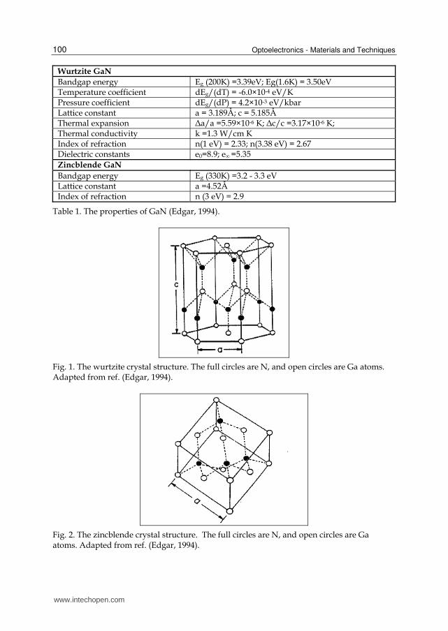
Wurtzite GaN Bandgap energy Eg (200K) =3.39eV; Eg(1.6K) = 3.50eV Temperature coefficient dEg/(dT) = -6.0×10⁻⁴ eV/K Pressure coefficient dEg/(dP) = 4.2×10⁻³ eV/kbar Lattice constant a = 3.189Å; c = 5.185Å Thermal expansion Δa/a =5.59×10⁻⁶ K; Δc/c =3.17×10⁻⁶ K; Thermal conductivity k =1.3 W/cm K Index of refraction n(1 eV) = 2.33; n(3.38 eV) = 2.67 Dielectric constants e0=8.9; e∞ =5.35 Zincblende GaN Bandgap energy Eg (330K) =3.2 - 3.3 eV Lattice constant a =4.52Å Index of refraction n (3 eV) = 2.9
Table 1. The properties of GaN (Edgar, 1994).
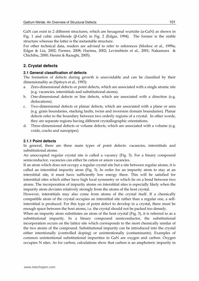
Fig. 1. The wurtzite crystal structure. The full circles are N, and open circles are Ga atoms. Adapted from ref. (Edgar, 1994).
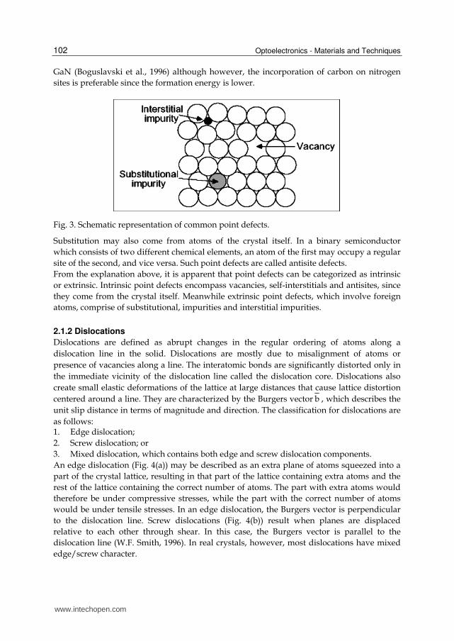
Fig. 2. The zincblende crystal structure. The full circles are N, and open circles are Ga atoms. Adapted from ref. (Edgar, 1994).
www.intechopen.com
Gallium Nitride: An Overview of Structural Defects
101
GaN can exist in 2 different structures, which are hexagonal wurtzite (┙-GaN) as shown in Fig. 1 and cubic zincblende (┚-GaN) in Fig. 2 (Edgar, 1994). The former is the stable structure whereas the latter is the metastable structure. For other technical data, readers are advised to refer to references (Morkoc et al., 1999a; Edgar & Liu, 2002; Parmer, 2008; Harima, 2002; Levinshtein et al., 2001; Nakamura & Chichibu, 2000; Henini & Razeghi, 2005).
2. Crystal defects
2.1 General classification of defects The formation of defects during growth is unavoidable and can be classified by their dimensionality as (Spitsyn et al., 1993): a. Zero-dimensional defects or point defects, which are associated with a single atomic site
(e.g. vacancies, interstitials and substitutional atoms). b. One-dimensional defects or line defects, which are associated with a direction (e.g.
dislocations). c. Two-dimensional defects or planar defects, which are associated with a plane or area
(e.g. grain boundaries, stacking faults, twins and inversion domain boundaries). Planar defects refer to the boundary between two orderly regions of a crystal. In other words, they are separate regions having different crystallographic orientations.
d. Three-dimensional defects or volume defects, which are associated with a volume (e.g. voids, cracks and nanopipes)
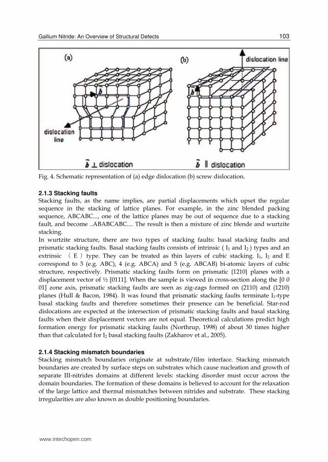
2.1.1 Point defects In general, there are three main types of point defects: vacancies, interstitials and substitutional atoms. An unoccupied regular crystal site is called a vacancy (Fig. 3). For a binary compound semiconductor, vacancies can either be cation or anion vacancies. If an atom which does not occupy a regular crystal site but a site between regular atoms, it is called an interstitial impurity atom (Fig. 3). In order for an impurity atom to stay at an interstitial site, it must have sufficiently low energy there. This will be satisfied for interstitial sites which either have high local symmetry or which lie on a bond between two atoms. The incorporation of impurity atoms on interstitial sites is especially likely when the impurity atom deviates relatively strongly from the atoms of the host crystal. However, interstitials may also come from atoms of the crystal itself. If a chemically compatible atom of the crystal occupies an interstitial site rather than a regular one, a self-interstitial is produced. For this type of point defect to develop in a crystal, there must be enough space between the host atoms, i.e. the crystal should not be packed too densely. When an impurity atom substitutes an atom of the host crystal (Fig. 3), it is referred to as a substitutional impurity. In a binary compound semiconductor, the substitutional incorporation occurs on the lattice site which corresponds to the most chemically similar of the two atoms of the compound. Substitutional impurity can be introduced into the crystal either intentionally (controlled doping) or unintentionally (contaminants). Examples of common unintentional substitutional impurities in GaN are oxygen and carbon. Oxygen occupies N sites. As for carbon, calculations show that carbon is an amphoteric impurity in
www.intechopen.com
Optoelectronics - Materials and Techniques
102
GaN (Boguslavski et al., 1996) although however, the incorporation of carbon on nitrogen sites is preferable since the formation energy is lower.
Fig. 3. Schematic representation of common point defects.
Substitution may also come from atoms of the crystal itself. In a binary semiconductor which consists of two different chemical elements, an atom of the first may occupy a regular site of the second, and vice versa. Such point defects are called antisite defects. From the explanation above, it is apparent that point defects can be categorized as intrinsic or extrinsic. Intrinsic point defects encompass vacancies, self-interstitials and antisites, since they come from the crystal itself. Meanwhile extrinsic point defects, which involve foreign atoms, comprise of substitutional, impurities and interstitial impurities.
2.1.2 Dislocations
Dislocations are defined as abrupt changes in the regular ordering of atoms along a dislocation line in the solid. Dislocations are mostly due to misalignment of atoms or presence of vacancies along a line. The interatomic bonds are significantly distorted only in the immediate vicinity of the dislocation line called the dislocation core. Dislocations also create small elastic deformations of the lattice at large distances that cause lattice distortion centered around a line. They are characterized by the Burgers vector b , which describes the unit slip distance in terms of magnitude and direction. The classification for dislocations are as follows: 1. Edge dislocation; 2. Screw dislocation; or 3. Mixed dislocation, which contains both edge and screw dislocation components. An edge dislocation (Fig. 4(a)) may be described as an extra plane of atoms squeezed into a part of the crystal lattice, resulting in that part of the lattice containing extra atoms and the rest of the lattice containing the correct number of atoms. The part with extra atoms would therefore be under compressive stresses, while the part with the correct number of atoms would be under tensile stresses. In an edge dislocation, the Burgers vector is perpendicular to the dislocation line. Screw dislocations (Fig. 4(b)) result when planes are displaced relative to each other through shear. In this case, the Burgers vector is parallel to the dislocation line (W.F. Smith, 1996). In real crystals, however, most dislocations have mixed edge/screw character.
www.intechopen.com
Gallium Nitride: An Overview of Structural Defects
103
Fig. 4. Schematic representation of (a) edge dislocation (b) screw dislocation.
2.1.3 Stacking faults Stacking faults, as the name implies, are partial displacements which upset the regular sequence in the stacking of lattice planes. For example, in the zinc blended packing sequence, ABCABC..., one of the lattice planes may be out of sequence due to a stacking fault, and become ..ABABCABC.... The result is then a mixture of zinc blende and wurtzite stacking. In wurtzite structure, there are two types of stacking faults: basal stacking faults and prismatic stacking faults. Basal stacking faults consists of intrinsic ( I1 and I2 ) types and an extrinsic 珙 E 珩type. They can be treated as thin layers of cubic stacking. I1, I2 and E correspond to 3 (e.g. ABC), 4 (e.g. ABCA) and 5 (e.g. ABCAB) bi-atomic layers of cubic structure, respectively. Prismatic stacking faults form on prismatic {1210} planes with a displacement vector of ½ [0111]. When the sample is viewed in cross-section along the [0 0 01] zone axis, prismatic stacking faults are seen as zig-zags formed on (2110) and (1210) planes (Hull & Bacon, 1984). It was found that prismatic stacking faults terminate I1-type basal stacking faults and therefore sometimes their presence can be beneficial. Star-rod dislocations are expected at the intersection of prismatic stacking faults and basal stacking faults when their displacement vectors are not equal. Theoretical calculations predict high formation energy for prismatic stacking faults (Northrup, 1998) of about 30 times higher than that calculated for I2 basal stacking faults (Zakharov et al., 2005).
2.1.4 Stacking mismatch boundaries Stacking mismatch boundaries originate at substrate/film interface. Stacking mismatch boundaries are created by surface steps on substrates which cause nucleation and growth of separate III-nitrides domains at different levels: stacking disorder must occur across the domain boundaries. The formation of these domains is believed to account for the relaxation of the large lattice and thermal mismatches between nitrides and substrate. These stacking irregularities are also known as double positioning boundaries.
www.intechopen.com
Optoelectronics - Materials and Techniques
104
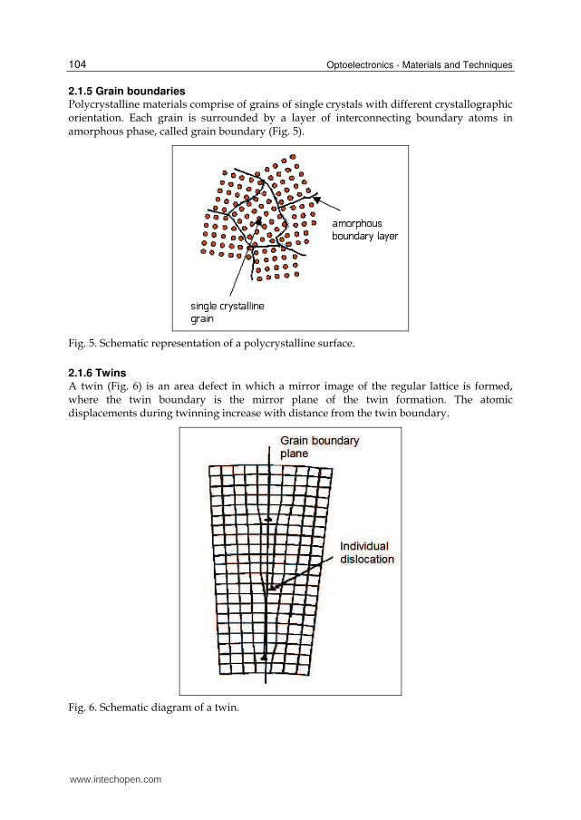
2.1.5 Grain boundaries Polycrystalline materials comprise of grains of single crystals with different crystallographic orientation. Each grain is surrounded by a layer of interconnecting boundary atoms in amorphous phase, called grain boundary (Fig. 5).
Fig. 5. Schematic representation of a polycrystalline surface.
2.1.6 Twins A twin (Fig. 6) is an area defect in which a mirror image of the regular lattice is formed, where the twin boundary is the mirror plane of the twin formation. The atomic displacements during twinning increase with distance from the twin boundary.
Fig. 6. Schematic diagram of a twin.
www.intechopen.com
Gallium Nitride: An Overview of Structural Defects
105
2.1.7 Inversion domains This defect originates from the nucleation layer and has a filamentary nature. Inversion domains may not be easily distinguished from pure dislocations (Ponce et al., 1997).
2.1.8 Nanopipes They are tunnel-like defects which are aligned along the growth direction of the crystal and penetrate the film. Like inversion domains, they have a filamentary nature and may not be easily distinguished from pure dislocations (Ponce et al., 1997).
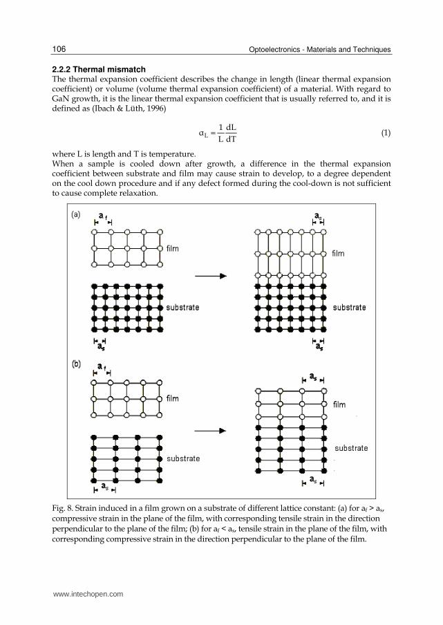
2.2 Crystal defects caused by strain One of the causes of defects is the strain due to lattice and thermal mismatch between film and substrate. The lattice and thermal mismatch induce residual strain in the III-V nitrides films (the term “residual” emphasizes the fact that the stress remains after all external forces are removed). When speaking of strain generated due to mismatch with the substrate, it is usually in reference to the biaxial strain in the plane of the layer (i.e. along the a-axis) (Fig. 7). In the perpendicular direction (i.e along the c-axis), there will be a corresponding strain. Because strain in thin films is governed by both lattice and thermal mismatch, the dominating strain contribution will be determined by growth conditions such as growth temperature and the degree of the mismatch.
Fig. 7. Biaxial strain (white arrows) in a film grown on a lattice and thermally-mismatched substrate: (a) compressive strain (black arrow indicates the corresponding tensile strain in the perpendicular direction); (b) tensile strain (black arrow indicates the corresponding compressive strain in the perpendicular direction).
2.2.1 Lattice mismatch When a film is grown on a substrate of different lattice constant, the film will expand (tensile strain) or contract (compressive strain) to accommodate the different lattice constant of the substrate. The type of strain which the film will be subjected to depend on whether the lattice constant is larger or smaller than that of the substrate. If the lattice constant of the film is larger than that of the substrate, the film will be subjected to compressive strain but if the lattice constant of the film is smaller than that of the substrate, the film will be under tensile strain (Fig. 8). Technically, a compressive strain in the film should go hand in hand with a tensile strain in the substrate, and vice versa. However, the substrate experiences negligible expansion or contraction due to its much larger thickness in comparison to the film. As a note, the lattice constant value of III-V nitrides is influenced by the growth conditions, impurity concentrations and film stoichiometry.
www.intechopen.com
Optoelectronics - Materials and Techniques
106
2.2.2 Thermal mismatch The thermal expansion coefficient describes the change in length (linear thermal expansion coefficient) or volume (volume thermal expansion coefficient) of a material. With regard to GaN growth, it is the linear thermal expansion coefficient that is usually referred to, and it is defined as (Ibach & Lüth, 1996)
L1 dL┙L dT
= (1)
where L is length and T is temperature. When a sample is cooled down after growth, a difference in the thermal expansion coefficient between substrate and film may cause strain to develop, to a degree dependent on the cool down procedure and if any defect formed during the cool-down is not sufficient to cause complete relaxation.
Fig. 8. Strain induced in a film grown on a substrate of different lattice constant: (a) for af > as, compressive strain in the plane of the film, with corresponding tensile strain in the direction perpendicular to the plane of the film; (b) for af < as, tensile strain in the plane of the film, with corresponding compressive strain in the direction perpendicular to the plane of the film.
www.intechopen.com
Gallium Nitride: An Overview of Structural Defects
107
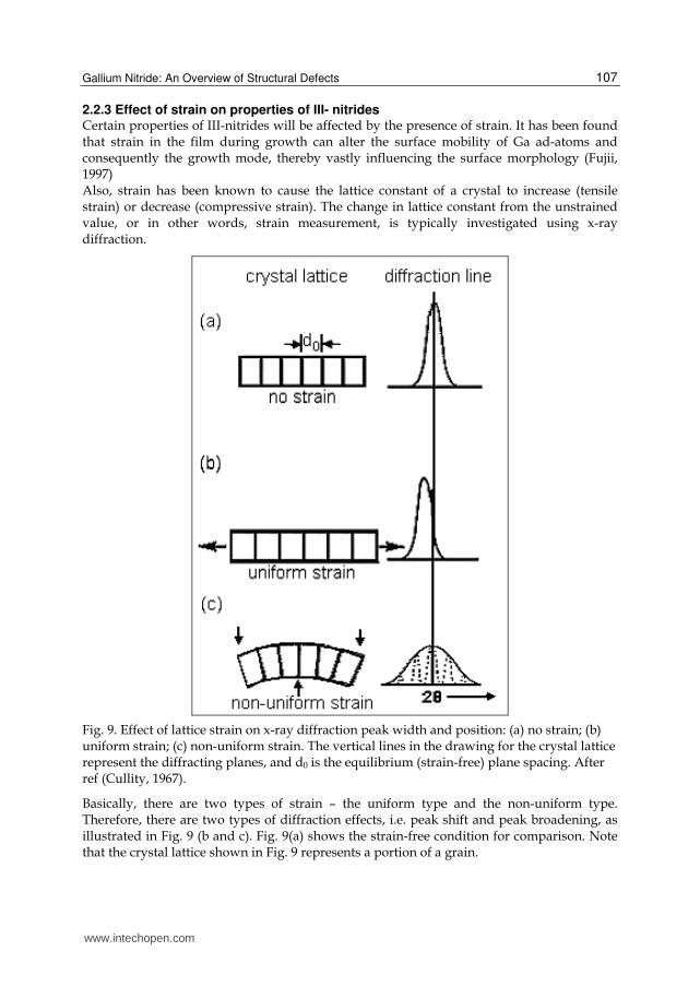
2.2.3 Effect of strain on properties of III- nitrides Certain properties of III-nitrides will be affected by the presence of strain. It has been found that strain in the film during growth can alter the surface mobility of Ga ad-atoms and consequently the growth mode, thereby vastly influencing the surface morphology (Fujii, 1997) Also, strain has been known to cause the lattice constant of a crystal to increase (tensile strain) or decrease (compressive strain). The change in lattice constant from the unstrained value, or in other words, strain measurement, is typically investigated using x-ray diffraction.
Fig. 9. Effect of lattice strain on x-ray diffraction peak width and position: (a) no strain; (b) uniform strain; (c) non-uniform strain. The vertical lines in the drawing for the crystal lattice represent the diffracting planes, and d0 is the equilibrium (strain-free) plane spacing. After ref (Cullity, 1967).
Basically, there are two types of strain – the uniform type and the non-uniform type. Therefore, there are two types of diffraction effects, i.e. peak shift and peak broadening, as illustrated in Fig. 9 (b and c). Fig. 9(a) shows the strain-free condition for comparison. Note that the crystal lattice shown in Fig. 9 represents a portion of a grain.
www.intechopen.com
Optoelectronics - Materials and Techniques
108
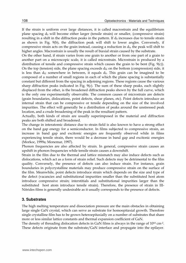
If the strain is uniform over large distances, it is called macrostrain and the equilibrium plane spacing d0 will become either larger (tensile strain) or smaller, (compressive strain) resulting in a shift in the diffraction peaks in the pattern. If d0 increases due to tensile strain as shown in Fig. 9(b), the diffraction peak will shift to lower angles. Conversely, if compressive strain acts on the grain instead, causing a reduction in d0, the peak will shift to higher angles. Macrostrain is usually the result of biaxial strain caused by the substrate. On the other hand, if strain varies from one grain to another or from one part of a grain to another part on a microscopic scale, it is called microstrain. Microstrain is produced by a distribution of tensile and compressive strain which causes the grain to be bent (Fig. 9(c)). On the top (tension) side, the plane spacing exceeds d0; on the bottom (compression) side, it is less than d0; somewhere in between, it equals d0. This grain can be imagined to be composed of a number of small regions in each of which the plane spacing is substantially constant but different from the spacing in adjoining regions. These regions cause the various sharp diffraction peaks indicated in Fig. 9(c). The sum of these sharp peaks, each slightly displaced from the other, is the broadened diffraction peaks shown by the full curve, which is the only one experimentally observable. The common causes of microstrain are defects (grain boundaries, dislocations, point defects, shear planes, etc). Point defects introduce an internal strain that can be compressive or tensile depending on the size of the involved impurities. The effect will generally be a distribution of peaks around the unstressed peak location, and a crude broadening of the peak in the resultant pattern. Actually, both kinds of strain are usually superimposed in the material and diffraction peaks are both shifted and broadened. The change in interatomic distance due to strain field is also known to have a strong effect on the band gap energy for a semiconductor. In films subjected to compressive strain, an increase in band gap and excitonic energies are frequently observed while in films experiencing tensile strain, there would be a decrease in band gap and excitonic energies (Morkoc, 1999a; Monemar, 1997). Phonon frequencies are also affected by strain. In general, compressive strain causes an upshift in phonon frequencies while tensile strain causes a downshift. Strain in the film due to the thermal and lattice mismatch may also induce defects such as dislocations, which act as a form of strain relief. Such defects may be detrimental to the film quality. Conversely, the presence of defects can also induce strain. For instance, grain boundaries in polycrystalline materials may produce compressive strain on the surface of the film. Meanwhile, point defects introduce strain which depends on the size and type of the defect (vacancies and substitutional impurities smaller than the substituted host atom introduce compressive strain; interstitials and substitutional impurities larger than the substituted host atom introduce tensile strain). Therefore, the presence of strain in III-Nitrides films is generally undesirable as it usually corresponds to the presence of defects.
3. Substrates
The high melting temperature and dissociation pressure are the main obstacles in obtaining large single GaN crystal, which can serve as substrate for homoepitaxial growth. Therefore single crystalline film has to be grown heteroepitaxially on a number of substrates that share more or less similar lattice constants and thermal expansion coefficient of GaN. The density of threading dislocation defects in GaN films is always in the range of 1010 cm-2. These defects originate from the substrate/GaN interface and propagate into the epilayer.
www.intechopen.com
Gallium Nitride: An Overview of Structural Defects
109
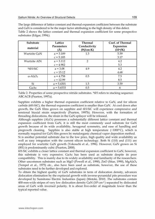
The large difference of lattice constant and thermal expansion coefficient between the substrate and GaN is considered to be the major factor attributing to the high density of this defect. Table 2 shows the lattice constant and thermal expansion coefficient for some prospective substrates (Edgar, 1994;).
Substrate Lattice Thermal Coef. of Thermal
material Parameters
(Å) Conductivity
(W/cm-K) Expansion
(10-6/K) Wurtzite GaN a = 3.189 1.3 5.59
c = 5.185 3.17 Wurtzite AlN a = 3.112 2 4.2
c = 4.982 5.3 *6H-SiC a = 3.08 4.9 4.2
c = 15.12 4.68 ┙-Al2O3 a = 4.758 0.5 7.5
c = 12.99 8.5 Si a = 5.4301 1.5 3.59
GaAs a = 5.6533 0.5 6
Table 2. Properties of some prospective nitride substrates. *6H refers to stacking sequence: ABCACB (Pearton, 1997a).
Sapphire exhibits a higher thermal expansion coefficient relative to GaN, and for silicon carbide (6H-SiC), the thermal expansion coefficient is smaller than GaN. At cool down after growth, the GaN films grown on sapphire and 6H-SiC will experience compressive and tensional biaxial strain respectively (Pearton, 1997b). However, with the formation of threading dislocations, the strain in the GaN epilayer will be released. Although sapphire (Al2O3) possesses a substantially different lattice constant and thermal expansion coefficient from GaN, it is still the most commonly used substrate for GaN growth because of its wide availability, hexagonal symmetry, and ease of handling and pregrowth cleaning. Sapphire is also stable at high temperature (~1000°C), which is normally required for GaN film grown by metalorganic chemical vapor deposition method. Si is another potential substrate due to the low price, high quality and wide availability as well as easy integration with the current silicon technology. Both Si (110) and (111) are employed for wurtzitic GaN growth (Yokouchi et al., 1996). However, GaN grown on Si (001) is predominantly cubic (Pearton, 2000). 6H-SiC exhibits a closer lattice constant and thermal expansion coefficient to GaN, however, this substrate is very expensive. GaAs has been used as substrate despite its poor compatibility. This is mainly due to its widely availability and familiarity of the researchers. Other uncommon substrates such as MgO (Powell et al., 1990), ZnO (Sitar, 1990), MgAl2O4 (Tempel et al., 1975) etc., also have been used as substrate, however, the use of these substrates need to be further developed and explored. To obtain the highest quality of GaN substrates in term of dislocation density, advances dislocation elimination by the expitaxial growth with inverse-pyramidal pits procedure was developed by Sumitomo Electric Industries (Japan) (Motoki, 2010) .The substrates contain 400-mm-wide stripes of very low dislocation density GaN (105 cm-2 ) separated by dislocated areas of GaN with inversed polarity. It is about five-order of magnitude lower than the typical reported value.
www.intechopen.com
Optoelectronics - Materials and Techniques
110
4. Defects in GaN films and formation mechanisms
4.1 Threading dislocation D. Kapolnek (Kapolnek et al., 1995) proposed that in GaN films grown by metalorganic chemical vapor deposition on sapphire, the source for dislocation is the nucleation layer itself. During island coalescence, edge threading dislocation segments may be generated when misfit edge dislocations between adjacent island are spatially out of phase. The generation of screw dislocations appears to be more complex, they found out that pure screw or mixed threading dislocations do decrease with the film thickness, due to the ease of cross slip of screw dislocations. Kyoyeol Lee (Lee & Auh, 2001) studied the dislocation density of GaN on sapphire grown by hydride vapor phase epitaxy. They found that the reduction of threading dislocation sites occurred with increasing GaN films thickness. Similarly, F. R. Chien (Chien et al., 1996) also investigated growth defects in GaN films grown by metalorganic chemical vapor deposition on 6H-SiC substrate, and reported that dislocation density decreases rapidly with the increase of GaN film thickness from the interface. The predominant defects in GaN films grown on 6H-SiC with aluminium nitride (AlN) buffer layer are edge type threading dislocations along [0001] growth direction with Burgers vector 1/3 <12 1 0>. The reduction in dislocation density is due to the formation of half-loops. Besides this, dislocation reaction also plays a role, for example, two dislocations interact and merge to produce one dislocation, according to the reaction:
1 11210 0001 12133 3− −
+ →⎡ ⎤⎣ ⎦ (2)
These dislocations originated at AlN/SiC interface to accommodate the misorientation of neighboring domains formed from initial island nuclei, which are twisted and tilted with respect to the substrate surface.
4.2 Stacking faults There have been reported that stacking faults formed in GaN layers grown on polar and non-polar substrates are different. For the growth in polar direction, stacking faults are formed on the basal plane (c-plane) since their formation energy is the lowest on this plane. If growth is taking place on the c-surface, these faults will be located on planes parallel to the substrate (Fig. 10(a)). While for the growth in non-polar direction, stacking faults are formed on basal planes (c- planes) that are along growth direction (Liliental-Weber, 2008), since their formation energy on these planes is the lowest and they will be arranged perpendicular to the substrate (Fig. 10(b)). On the other hand, F. Gloux (Gloux et al., 2008) studied the structural defects of GaN implanted with rare earth ions at room temperature and 500◦C. The crystallographic damage induced in GaN by 300 keV rare earth ions implantation has been investigated as a function of the implantation temperature. It consists of point defect clusters, basal and prismatic stacking faults. The majority of basal stacking faults is I1. The density of stacking faults after 500°C implantation is significantly smaller than after implantation at room temperature.
www.intechopen.com
Gallium Nitride: An Overview of Structural Defects
111
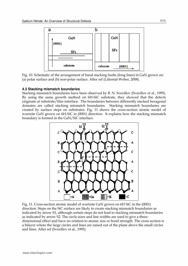
Fig. 10. Schematic of the arrangement of basal stacking faults (long lines) in GaN grown on: (a) polar surface and (b) non-polar surface. After ref (Liliental-Weber, 2008).
4.3 Stacking mismatch boundaries Stacking mismatch boundaries have been observed by B. N. Sverdlov (Sverdlov et al., 1995). By using the same growth method on 6H-SiC substrate, they showed that the defects originate at substrate/film interface. The boundaries between differently stacked hexagonal domains are called stacking mismatch boundaries. Stacking mismatch boundaries are created by surface steps on substrates. Fig. 11 shows the cross-section atomic model of wurtzite GaN grown on 6H-SiC in (0001) direction. It explains how the stacking mismatch boundary is formed in the GaN/SiC interface.
Fig. 11. Cross-section atomic model of wurtzite GaN grown on 6H SiC in the (0001) direction. Steps on the SiC surface are likely to create stacking mismatch boundaries as indicated by arrow S1, although certain steps do not lead to stacking mismatch boundaries as indicated by arrow S2. The circle sizes and line widths are used to give a three-dimensional effect and have no relation to atomic size or bond strength. The cross section is a bilayer where the large circles and lines are raised out of the plane above the small circles and lines. After ref (Sverdlov et al., 1995).
www.intechopen.com
Optoelectronics - Materials and Techniques
112
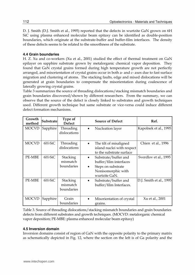
D. J. Smith (D.J. Smith et al., 1995) reported that the defects in wurtzite GaN grown on 6H SiC using plasma enhanced molecular beam epitaxy can be identified as double-position boundaries, which originate at the substrate-buffer and buffer-film interfaces. The density of these defects seems to be related to the smoothness of the substrate.
4.4 Grain boundaries H. Z. Xu and co-workers (Xu et al., 2001) studied the effect of thermal treatment on GaN epilayer on sapphire substrate grown by metalorganic chemical vapor deposition. They found that GaN crystal grains formed during high temperature growth are not perfectly arranged, and misorientation of crystal grains occur in both a- and c- axes due to fast surface migration and clustering of atoms. The stacking faults, edge and mixed dislocations will be generated at grain boundaries to compensate the misorientation during coalescence of laterally growing crystal grains. Table 3 summarizes the source of threading dislocations/stacking mismatch boundaries and grain boundaries discovered/shown by different researchers. From the summary, we can observe that the source of the defect is closely linked to substrates and growth techniques used. Different growth technique but same substrate or vice-versa could induce different defect formation mechanisms.
Growth method
SubstrateType of Defect
Source of Defect Ref.
MOCVD Sapphire Threading dislocations
• Nucleation layer Kapolnek et al., 1995
MOCVD 6H-SiC Threading dislocations
• The tilt of misaligned island nuclei with respect to the substrate surface
Chien et al., 1996
PE-MBE 6H-SiC Stacking mismatch
boundaries
• Substrate/buffer and buffer/film interfaces
• Steps on substrate Nonisomorphic with
wurtzite GaN.
Sverdlov et al., 1995
PE-MBE 6H-SiC Stacking mismatch
boundaries
• Substrate/buffer and buffer/film Interfaces.
D.J. Smith et al., 1995
MOCVD Sapphire Grain boundaries
• Misorientation of crystal grains.
Xu et al., 2001
Table 3. Source of threading dislocations/stacking mismatch boundaries and grain boundaries defects from different substrates and growth techniques. (MOCVD: metalorganic chemical vapor deposition; PE-MBE: plasma enhanced molecular beam epitaxy)
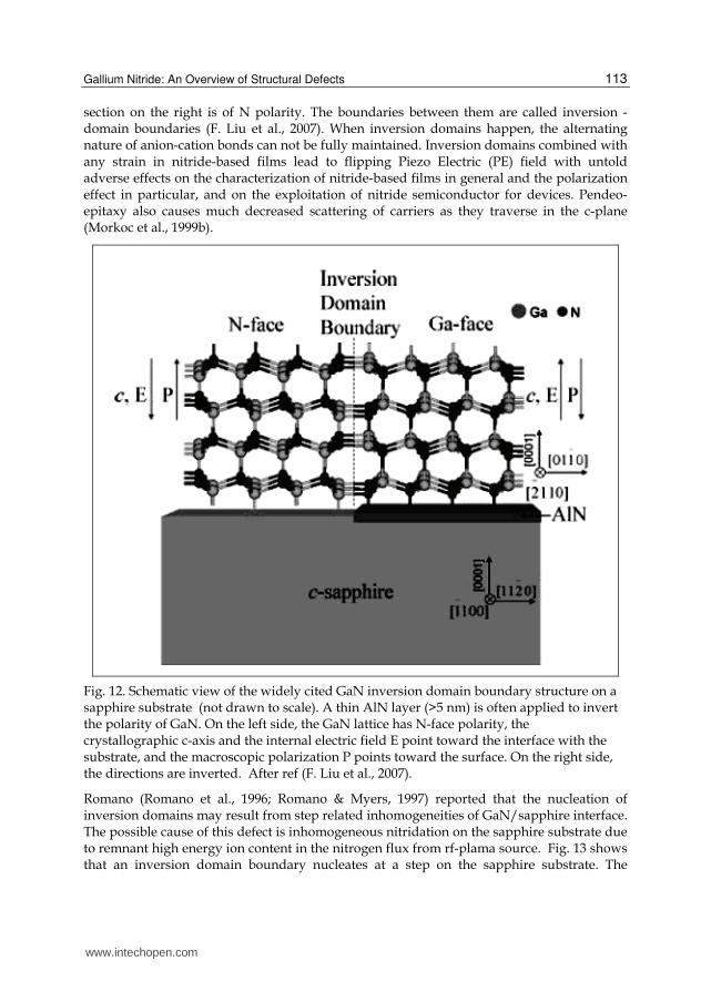
4.5 Inversion domain Inversion domains consist of region of GaN with the opposite polarity to the primary matrix as schematically depicted in Fig. 12, where the section on the left is of Ga polarity and the
www.intechopen.com
Gallium Nitride: An Overview of Structural Defects
113
section on the right is of N polarity. The boundaries between them are called inversion -domain boundaries (F. Liu et al., 2007). When inversion domains happen, the alternating nature of anion-cation bonds can not be fully maintained. Inversion domains combined with any strain in nitride-based films lead to flipping Piezo Electric (PE) field with untold adverse effects on the characterization of nitride-based films in general and the polarization effect in particular, and on the exploitation of nitride semiconductor for devices. Pendeo-epitaxy also causes much decreased scattering of carriers as they traverse in the c-plane (Morkoc et al., 1999b).
Fig. 12. Schematic view of the widely cited GaN inversion domain boundary structure on a sapphire substrate (not drawn to scale). A thin AlN layer (>5 nm) is often applied to invert the polarity of GaN. On the left side, the GaN lattice has N-face polarity, the crystallographic c-axis and the internal electric field E point toward the interface with the substrate, and the macroscopic polarization P points toward the surface. On the right side, the directions are inverted. After ref (F. Liu et al., 2007).
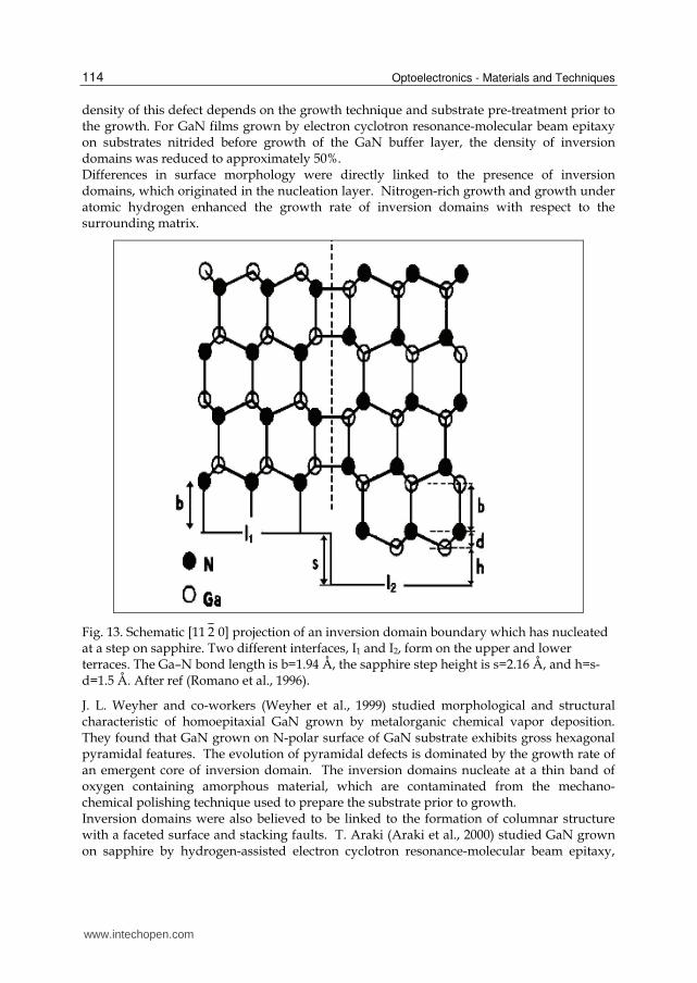
Romano (Romano et al., 1996; Romano & Myers, 1997) reported that the nucleation of inversion domains may result from step related inhomogeneities of GaN/sapphire interface. The possible cause of this defect is inhomogeneous nitridation on the sapphire substrate due to remnant high energy ion content in the nitrogen flux from rf-plama source. Fig. 13 shows that an inversion domain boundary nucleates at a step on the sapphire substrate. The
www.intechopen.com
Optoelectronics - Materials and Techniques
114
density of this defect depends on the growth technique and substrate pre-treatment prior to the growth. For GaN films grown by electron cyclotron resonance-molecular beam epitaxy on substrates nitrided before growth of the GaN buffer layer, the density of inversion domains was reduced to approximately 50%. Differences in surface morphology were directly linked to the presence of inversion domains, which originated in the nucleation layer. Nitrogen-rich growth and growth under atomic hydrogen enhanced the growth rate of inversion domains with respect to the surrounding matrix.
Fig. 13. Schematic [11 2 0] projection of an inversion domain boundary which has nucleated at a step on sapphire. Two different interfaces, I1 and I2, form on the upper and lower terraces. The Ga–N bond length is b=1.94 Å, the sapphire step height is s=2.16 Å, and h=s-d=1.5 Å. After ref (Romano et al., 1996).
J. L. Weyher and co-workers (Weyher et al., 1999) studied morphological and structural characteristic of homoepitaxial GaN grown by metalorganic chemical vapor deposition. They found that GaN grown on N-polar surface of GaN substrate exhibits gross hexagonal pyramidal features. The evolution of pyramidal defects is dominated by the growth rate of an emergent core of inversion domain. The inversion domains nucleate at a thin band of oxygen containing amorphous material, which are contaminated from the mechano-chemical polishing technique used to prepare the substrate prior to growth. Inversion domains were also believed to be linked to the formation of columnar structure with a faceted surface and stacking faults. T. Araki (Araki et al., 2000) studied GaN grown on sapphire by hydrogen-assisted electron cyclotron resonance-molecular beam epitaxy,
www.intechopen.com
Gallium Nitride: An Overview of Structural Defects
115
and found that GaN layer change from 2-dimension to 3-dimension growth by adding hydrogen to nitrogen plasma. They assumed that the inversion domains of polarity existed on the buffer layer, which led to the formation of this defect. The origin of inversion domains in Ga polar on GaN is not well defined. In the paper (Łucznik et al., 2009), it showed that most probably they were formed because of some technical reasons (e.g imperfect substrate preparation). According to J.L. Weyher (Weyher et al., 2010), the simple methods to recognize the present of inversion domains are hot KOH water solution, molten eutectic of KOH/NaOH and photo-etching. B. Barbaray (Barbaray et al., 1999) reported inversion domains were generated at substrate steps in GaN/(0001) Al2O3 layers. Steps of height c-Substrate/3=0.433 nm were found to give rise to extended defects in the epitaxial layer. These defects were inversion domains whose boundary atomic structure was found to be described by the Holt model. The investigation of steps on the substrate showed that discontinuities of the substrate surface create defects in the deposited layers. They proposed that inversion domains can be due to the mismatch along c between the substrate and the deposit. A geometrical analysis showed that the formation of Holt or inversion domain boundaries minimizing the shift along the growth axis. A.M. Sa´nchez (Sa´nchez et al., 2002) studied the AlN buffer layer thickness influence on inversion domains in GaN/AlN/Si(111) heterostructures grown by plasma assisted molecular beam epitaxy. Inversion domains density inside the GaN epilayers, is higher in the sample with a smaller buffer layer thickness. The N-polarity leads to a higher inversion domains density when reaching the GaN surface.
4.6 Nanopipes
Another type of defect found in GaN films is nanopipes, also called micropipes by some researchers. This defect has the character of open core screw dislocation. The oxygen impurity is considered to be closely linked with the formation of this defect by poisoning the exposed facet walls thereby preventing complete layer coalescence. There is evidence from the observation of void formation along dislocations. Speculation is made on a generalized pipe diffusion mechanism for the loss of oxygen from GaN/sapphire interface during growth. This leads to the poisoning of {10 1 0} side walls that allows nanopipes to propagate, or to the formation of void (Brown, 2000). W. Qian (Qian, 1995b) reported similar type of defect in GaN film on c-plane sapphire grown by metalorganic chemical vapor deposition. Tunnel-like defects are observed and aligned along the growth direction of crystal and penetrate the epilayer. This provides evidence that the nanopipes occur at the core of screw dislocation. However they did not elaborate clearly about the formation mechanism of this structural defect. Elsner (Elsner et al., 1998) studied the effect of oxygen on GaN surfaces grown by vapor phase epitaxy on sapphire. They found that oxygen has a tendency to segregate to the (10 1 0) surface and identified the gallium vacancy surrounded by 3 oxygen (where 3 nitrogen atoms were replaced) impurities [VGa -(ON)3] to be a stable and inert complex. These defects increase in concentration when internal surfaces grow out. When a critical concentration of the order of a monolayer is reached further growth is prevented. A schematic defect complex model was proposed (Fig. 14) based on the calculation of the defect formation energy.
www.intechopen.com
Optoelectronics - Materials and Techniques
116
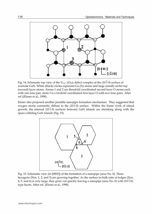
Fig. 14. Schematic top view of the VGa– (ON)3 defect complex at the (10 1 0) surface of wurtzite GaN. White (black) circles represent Ga (N) atoms and large (small) circles top (second) layer atoms. Atoms 1 and 2 are threefold coordinated second layer O atoms each with one lone pair, atom 3 is a twofold coordinated first layer O with two lone pairs. After ref ((Elsner et al., 1998) .
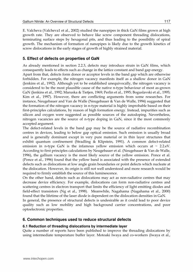
Elsner also proposed another possible nanopipe formation mechanism. They suggested that oxygen atoms constantly diffuse to the (10 1 0) surface. Within the frame work of island growth, the internal (10 1 0) surfaces between GaN islands are shrinking along with the space colliding GaN islands (Fig. 15).
Fig. 15. Schematic view (in [0001]) of the formation of a nanopipe (area No. 0). Three hexagons (Nos. 1, 2, and 3) are growing together. As the surface to-bulk ratio at ledges (Nos. 4, 5, and 6) is very large, they grow out quickly leaving a nanopipe (area No. 0) with {10 1 0}-type facets. After ref. (Elsner et al., 1998) .
www.intechopen.com
Gallium Nitride: An Overview of Structural Defects
117
E. Valcheva (Valcheva1 et al., 2002) studied the nanopipes in thick GaN films grown at high growth rate. They are observed to behave like screw component threading dislocations, terminating surface steps by hexagonal pits, and thus leading to the possibility of spiral growth. The mechanism of formation of nanopipes is likely due to the growth kinetics of screw dislocations in the early stages of growth of highly strained material.
5. Effect of defects on properties of GaN
As already mentioned in section 2.2.3, defects may introduce strain in GaN films, which consequently leads to effects such as change in the lattice constant and band gap energy. Apart from that, defects form donor or acceptor levels in the band gap which are otherwise forbidden. For example, the nitrogen vacancy manifests itself as a shallow donor in GaN (Jenkins et al., 1992). Although yet to be established unequivocally, the nitrogen vacancy is considered to be the most plausible cause of the native n-type behaviour of most as-grown GaN (Jenkins et al., 1992; Maruska & Tietjen, 1969; Perlin et al., 1995; Boguslavski et al., 1995; Kim et al., 1997). However, there are conflicting arguments from some researches. For instance, Neugebauer and Van de Walle (Neugebauer & Van de Walle, 1994) suggested that the formation of the nitrogen vacancy in n-type material is highly improbable based on their first-principles calculations, by reason of high formation energy. Instead, impurities such as silicon and oxygen were suggested as possible sources of the autodoping. Nevertheless, nitrogen vacancies are the source of n-type doping in GaN, since it the most commonly accepted argument. The defect-related levels in the band gap may be the source of radiative recombination centres in devices, leading to below gap optical emission. Such emission is usually broad and is generally dominant except in very pure material or in thin layer structures that exhibit quantum confinement (Stradling & Klipstein, 1991). A common defect-related emission in n-type GaN is the infamous yellow emission which occurs at ~ 2.2.eV. According to first principles calculations by Neugebauer et al. (Neugebauer & Van de Walle, 1996), the gallium vacancy is the most likely source of the yellow emission. Ponce et al. (Ponce et al., 1996) found that the yellow band is associated with the presence of extended defects such as dislocations at low angle grain boundaries or point defects which nucleate at the dislocation. However, its origin is still not well understood and more research would be required to firmly establish the source of this luminescence. On the other hand, defects such as dislocations may act as non-radiative centres that may decrease device efficiency. For example, dislocations can form non-radiative centres and scattering centres in electron transport that limits the efficiency of light emitting diodes and field-effect transistors (Ng et al., 1998). Meanwhile, Nagahama (Nagahama et al., 2000) found that the lifetime of the laser diode is dependent on the dislocation densities in GaN. In general, the presence of structural defects is undesirable as it could lead to poor device quality such as low mobility and high background carrier concentrations, and poor optoelectronic properties.
6. Common techniques used to reduce structural defects
6.1 Reduction of threading dislocations by intermediate layer Quite a number of reports have been published to improve the threading dislocations by using intermediate temperature buffer layer. Motoaki Iwaya and co-workers (Iwaya et al.,
www.intechopen.com
Optoelectronics - Materials and Techniques
118
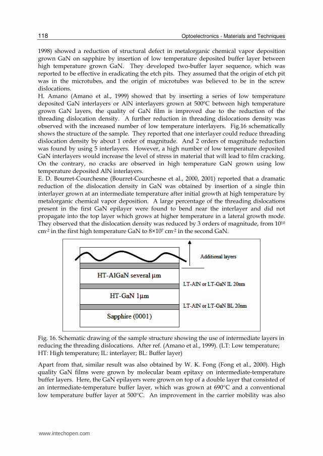
1998) showed a reduction of structural defect in metalorganic chemical vapor deposition grown GaN on sapphire by insertion of low temperature deposited buffer layer between high temperature grown GaN. They developed two-buffer layer sequence, which was reported to be effective in eradicating the etch pits. They assumed that the origin of etch pit was in the microtubes, and the origin of microtubes was believed to be in the screw dislocations. H. Amano (Amano et al., 1999) showed that by inserting a series of low temperature deposited GaN interlayers or AlN interlayers grown at 500ºC between high temperature grown GaN layers, the quality of GaN film is improved due to the reduction of the threading dislocation density. A further reduction in threading dislocations density was observed with the increased number of low temperature interlayers. Fig.16 schematically shows the structure of the sample. They reported that one interlayer could reduce threading dislocation density by about 1 order of magnitude. And 2 orders of magnitude reduction was found by using 5 interlayers. However, a high number of low temperature deposited GaN interlayers would increase the level of stress in material that will lead to film cracking. On the contrary, no cracks are observed in high temperature GaN grown using low temperature deposited AlN interlayers. E. D. Bourret-Courchesne (Bourret-Courchesne et al., 2000, 2001) reported that a dramatic reduction of the dislocation density in GaN was obtained by insertion of a single thin interlayer grown at an intermediate temperature after initial growth at high temperature by metalorganic chemical vapor deposition. A large percentage of the threading dislocations present in the first GaN epilayer were found to bend near the interlayer and did not propagate into the top layer which grows at higher temperature in a lateral growth mode. They observed that the dislocation density was reduced by 3 orders of magnitude, from 1010 cm-2 in the first high temperature GaN to 8×107 cm-2 in the second GaN.
Fig. 16. Schematic drawing of the sample structure showing the use of intermediate layers in reducing the threading dislocations. After ref. (Amano et al., 1999). (LT: Low temperature; HT: High temperature; IL: interlayer; BL: Buffer layer)
Apart from that, similar result was also obtained by W. K. Fong (Fong et al., 2000). High quality GaN films were grown by molecular beam epitaxy on intermediate-temperature buffer layers. Here, the GaN epilayers were grown on top of a double layer that consisted of an intermediate-temperature buffer layer, which was grown at 690°C and a conventional low temperature buffer layer at 500°C. An improvement in the carrier mobility was also
www.intechopen.com
Gallium Nitride: An Overview of Structural Defects
119
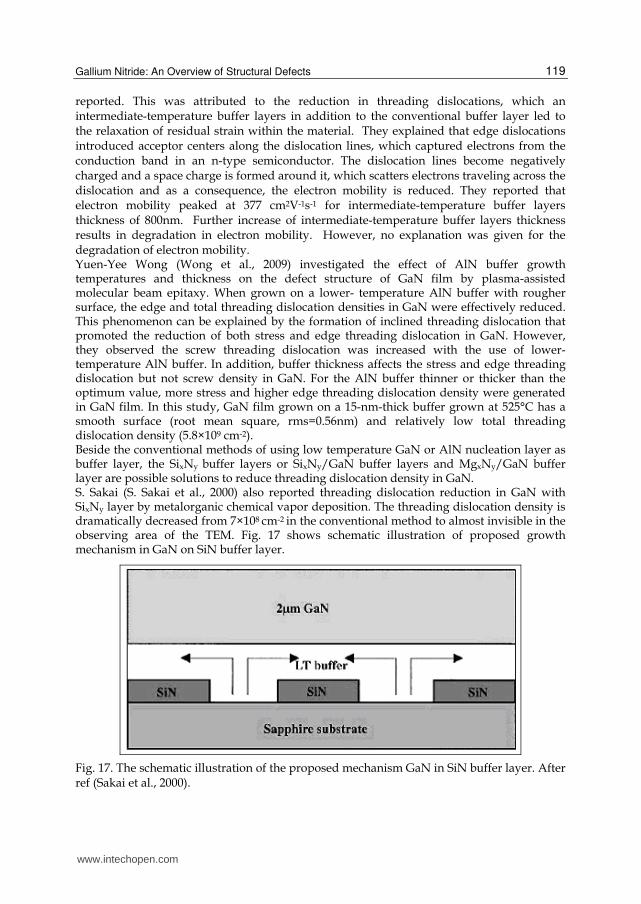
reported. This was attributed to the reduction in threading dislocations, which an intermediate-temperature buffer layers in addition to the conventional buffer layer led to the relaxation of residual strain within the material. They explained that edge dislocations introduced acceptor centers along the dislocation lines, which captured electrons from the conduction band in an n-type semiconductor. The dislocation lines become negatively charged and a space charge is formed around it, which scatters electrons traveling across the dislocation and as a consequence, the electron mobility is reduced. They reported that electron mobility peaked at 377 cm2V-1s-1 for intermediate-temperature buffer layers thickness of 800nm. Further increase of intermediate-temperature buffer layers thickness results in degradation in electron mobility. However, no explanation was given for the degradation of electron mobility. Yuen-Yee Wong (Wong et al., 2009) investigated the effect of AlN buffer growth temperatures and thickness on the defect structure of GaN film by plasma-assisted molecular beam epitaxy. When grown on a lower- temperature AlN buffer with rougher surface, the edge and total threading dislocation densities in GaN were effectively reduced. This phenomenon can be explained by the formation of inclined threading dislocation that promoted the reduction of both stress and edge threading dislocation in GaN. However, they observed the screw threading dislocation was increased with the use of lower-temperature AlN buffer. In addition, buffer thickness affects the stress and edge threading dislocation but not screw density in GaN. For the AlN buffer thinner or thicker than the optimum value, more stress and higher edge threading dislocation density were generated in GaN film. In this study, GaN film grown on a 15-nm-thick buffer grown at 525°C has a smooth surface (root mean square, rms=0.56nm) and relatively low total threading dislocation density (5.8×109 cm-2). Beside the conventional methods of using low temperature GaN or AlN nucleation layer as buffer layer, the SixNy buffer layers or SixNy/GaN buffer layers and MgxNy/GaN buffer layer are possible solutions to reduce threading dislocation density in GaN. S. Sakai (S. Sakai et al., 2000) also reported threading dislocation reduction in GaN with SixNy layer by metalorganic chemical vapor deposition. The threading dislocation density is dramatically decreased from 7×108 cm-2 in the conventional method to almost invisible in the observing area of the TEM. Fig. 17 shows schematic illustration of proposed growth mechanism in GaN on SiN buffer layer.
Fig. 17. The schematic illustration of the proposed mechanism GaN in SiN buffer layer. After ref (Sakai et al., 2000).
www.intechopen.com
Optoelectronics - Materials and Techniques
120
Growth technique
Interlayer Improvement Ref.
MOCVD 2-buffer layer • Etch pits eradicated Iwaya
et al., 1998
1 interlayer • Threading dislocations reduced by 1 order magnitude MOCVD
5 interlayers • Threading dislocations reduced by 2 orders of magnitude
Amano et al., 1999
MOCVD Single interlayer • Threading dislocations reduced to 8×107 cm-2
Bourret-Courchesne et al., 2000,
2001
MBE
Double layer (intermediate-
temperature buffer layers + low
temperature buffer layer)
• Carrier mobility improved Fong
et al., 2000
PA-MBE
buffer layers were deposited at
different growth temperatures (from 450 to 840 °C) and thicknesses (from 4
to 30nm)
• GaN film grown on a 15-nm- thickbuffer grown at 525°C has a smooth surface (rms=0.56nm).
• Relatively low total threading dislocation density (5.8×109 cm-2).
Wong et al., 2009
MOCVD SixNy interlayer • Reduction in threading dislocationS. Sakai
et al., 2000
MOCVD in situ SixNy interlayers
• Threading dislocationdensity have been reduced from mid 109 cm-2 in the GaN template to 9×107 cm-2 with a coalescence thickness of 6 mm.
Kappers et al., 2007
MOCVD 2-buffer layers (MgxNy/AlN)
• Exhibits smaller x-ray diffraction FWHM of peak.
• Higher electron mobility, lower background concentration.
• Less etching pit density.
Wong et al., 2009
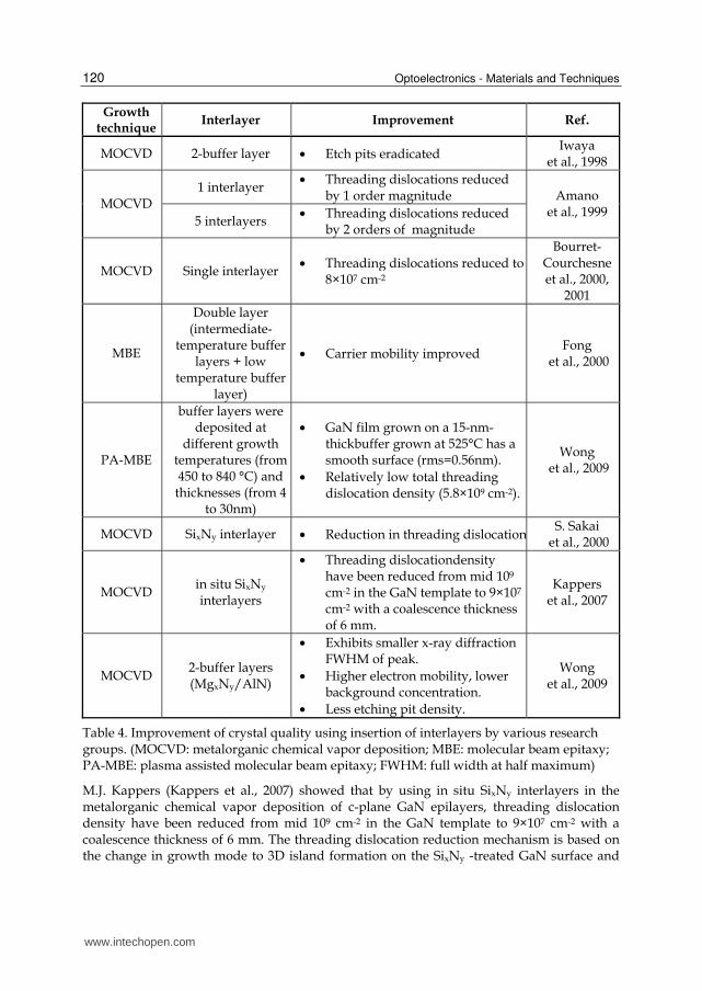
Table 4. Improvement of crystal quality using insertion of interlayers by various research groups. (MOCVD: metalorganic chemical vapor deposition; MBE: molecular beam epitaxy; PA-MBE: plasma assisted molecular beam epitaxy; FWHM: full width at half maximum)
M.J. Kappers (Kappers et al., 2007) showed that by using in situ SixNy interlayers in the metalorganic chemical vapor deposition of c-plane GaN epilayers, threading dislocation density have been reduced from mid 109 cm-2 in the GaN template to 9×107 cm-2 with a coalescence thickness of 6 mm. The threading dislocation reduction mechanism is based on the change in growth mode to 3D island formation on the SixNy -treated GaN surface and
www.intechopen.com
Gallium Nitride: An Overview of Structural Defects
121
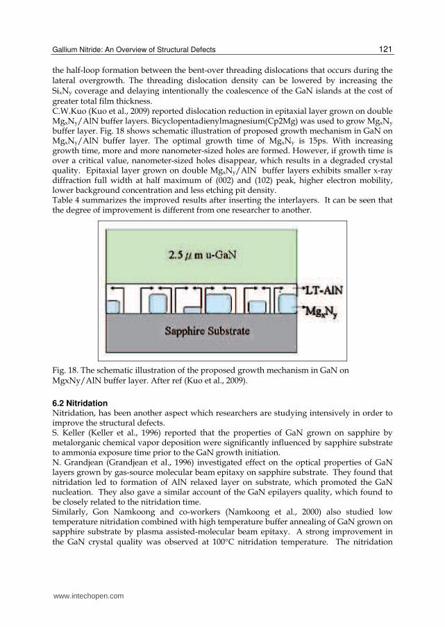
the half-loop formation between the bent-over threading dislocations that occurs during the lateral overgrowth. The threading dislocation density can be lowered by increasing the SixNy coverage and delaying intentionally the coalescence of the GaN islands at the cost of greater total film thickness. C.W.Kuo (Kuo et al., 2009) reported dislocation reduction in epitaxial layer grown on double MgxNy/AlN buffer layers. Bicyclopentadienylmagnesium(Cp2Mg) was used to grow MgxNy buffer layer. Fig. 18 shows schematic illustration of proposed growth mechanism in GaN on MgxNy/AlN buffer layer. The optimal growth time of MgxNy is 15ps. With increasing growth time, more and more nanometer-sized holes are formed. However, if growth time is over a critical value, nanometer-sized holes disappear, which results in a degraded crystal quality. Epitaxial layer grown on double MgxNy/AlN buffer layers exhibits smaller x-ray diffraction full width at half maximum of (002) and (102) peak, higher electron mobility, lower background concentration and less etching pit density. Table 4 summarizes the improved results after inserting the interlayers. It can be seen that the degree of improvement is different from one researcher to another.
Fig. 18. The schematic illustration of the proposed growth mechanism in GaN on MgxNy/AlN buffer layer. After ref (Kuo et al., 2009).
6.2 Nitridation Nitridation, has been another aspect which researchers are studying intensively in order to improve the structural defects. S. Keller (Keller et al., 1996) reported that the properties of GaN grown on sapphire by metalorganic chemical vapor deposition were significantly influenced by sapphire substrate to ammonia exposure time prior to the GaN growth initiation. N. Grandjean (Grandjean et al., 1996) investigated effect on the optical properties of GaN layers grown by gas-source molecular beam epitaxy on sapphire substrate. They found that nitridation led to formation of AlN relaxed layer on substrate, which promoted the GaN nucleation. They also gave a similar account of the GaN epilayers quality, which found to be closely related to the nitridation time. Similarly, Gon Namkoong and co-workers (Namkoong et al., 2000) also studied low temperature nitridation combined with high temperature buffer annealing of GaN grown on sapphire substrate by plasma assisted-molecular beam epitaxy. A strong improvement in the GaN crystal quality was observed at 100°C nitridation temperature. The nitridation
www.intechopen.com
Optoelectronics - Materials and Techniques
122
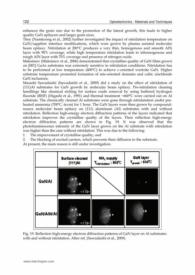
enhances the grain size due to the promotion of the lateral growth, this leads to higher quality GaN epilayers and larger grain sizes. They (Namkoong et al., 2002) further investigated the impact of nitridation temperature on GaN/sapphire interface modifications, which were grown by plasma assisted molecular beam epitaxy. Nitridation at 200°C produces a very thin, homogenous and smooth AlN layer with 90% coverage, while high temperature nitridation leads to inhomogenous and rough AlN layer with 70% coverage and presence of nitrogen oxide. Maksimov (Maksimov et al., 2006) demonstrated that crystalline quality of GaN films grown on [001] GaAs substrates was extremely sensitive to nitridation conditions. Nitridation has to be performed at low temperature (400ºC) to achieve c-oriented wurtzite GaN. Higher substrate temperature promoted formation of mis-oriented domains and cubic zincblende GaN inclusions. Masashi Sawadaishi (Sawadaishi et al., 2009) did a study on the effect of nitridation of (111)Al substrates for GaN growth by molecular beam epitaxy. Pre-nitridation cleaning handlings like chemical etching for surface oxide removal by using buffered hydrogen fluoride (BHF) (Higashi et al., 1991) and thermal treatment ~660°C were carried out on Al substrate. The chemically cleaned Al substrates were gone through nitridatation under pre-heated ammonia (700ºC, 6ccm) for 1 hour. The GaN layers were then grown by compound-source molecular beam epitaxy on (111) aluminum (Al) substrates with and without nitridation. Reflection high-energy electron diffraction patterns of the layers indicated that nitridation improves the crystalline quality of the layers. Their reflection high-energy electron diffraction patterns are shown in Fig. 19. It was observed that the photoluminescence intensity of the GaN layer grown on the Al substrate with nitridation was higher than the case without nitridation. This was due to the following: 1. The improvement of crystalline quality, and 2. The blocking of excited carriers, which prevents their diffusion to the substrate. At present, the main reason is still under investigation.
Fig. 19. Reflection high-energy electron diffraction patterns of GaN layer on Al substrates with and without nitridation. After ref. (Sawadaishi et al., 2009).
www.intechopen.com
Gallium Nitride: An Overview of Structural Defects
123
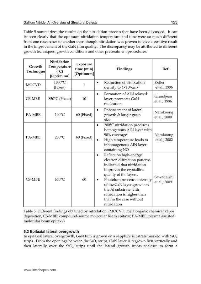
Table 5 summarizes the results on the nitridation process that have been discussed. It can be seen clearly that the optimum nitridation temperature and time were so much different from one researcher to another even though nitridation was proven to give a positive result in the improvement of the GaN film quality. The discrepancy may be attributed to different growth techniques, growth conditions and other pretreatment procedures.
Growth Technique
Nitridation Temperature
(°C) [Optimum]
Exposure time (min) [Optimum]
Findings Ref.
MOCVD 1050°C (Fixed)
1 • Reduction of dislocation
density to 4×108 cm-2 Keller et al., 1996
CS-MBE 850°C (Fixed) 10 • Formation of AlN relaxed
layer, promotes GaN nucleation
Grandjean et al., 1996
PA-MBE 100°C 60 (Fixed)• Enhancement of lateral
growth & larger grain size
Namkoong et al., 2000
PA-MBE 200°C 60 (Fixed)
• 200°C nitridation produces homogenous AlN layer with 90% coverage
• High temperature leads to inhomogenous AlN layer containing NO
Namkoong et al., 2002
CS-MBE 650°C 60
• Reflection high-energy electron diffraction patterns indicated that nitridation improves the crystalline quality of the layers.
• Photoluminescence intensity of the GaN layer grown on the Al substrate with nitridation is higher than that in the case without nitridation
Sawadaishi et al., 2009
Table 5. Different findings obtained by nitridation. (MOCVD: metalorganic chemical vapor deposition; CS-MBE: compound-source molecular beam epitaxy; PA-MBE: plasma assisted molecular beam epitaxy)
6.3 Epitaxial lateral overgrowth In epitaxial lateral overgrowth, GaN film is grown on a sapphire substrate masked with SiO2 strips. From the openings between the SiO2 strips, GaN layer is regrown first vertically and then laterally over the SiO2 strips until the lateral growth fronts coalesce to form a
www.intechopen.com
Optoelectronics - Materials and Techniques
124
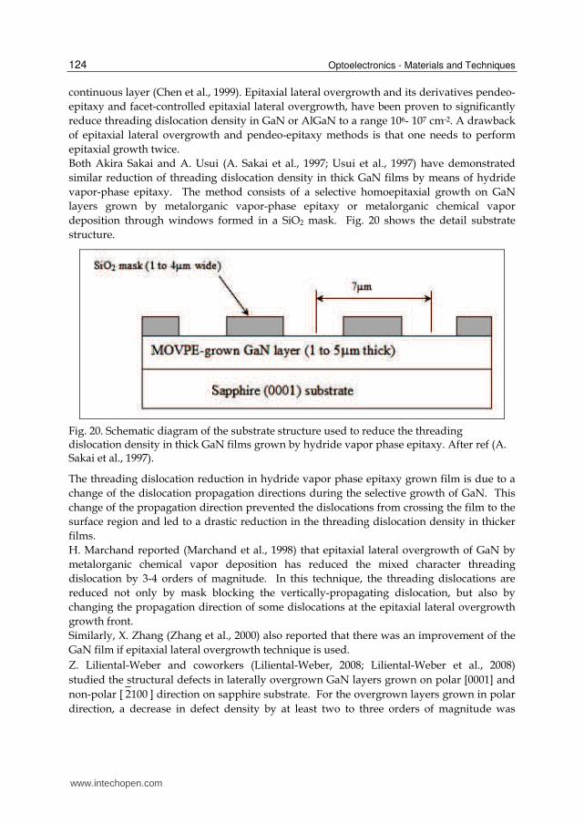
continuous layer (Chen et al., 1999). Epitaxial lateral overgrowth and its derivatives pendeo-epitaxy and facet-controlled epitaxial lateral overgrowth, have been proven to significantly reduce threading dislocation density in GaN or AlGaN to a range 106- 107 cm-2. A drawback of epitaxial lateral overgrowth and pendeo-epitaxy methods is that one needs to perform epitaxial growth twice. Both Akira Sakai and A. Usui (A. Sakai et al., 1997; Usui et al., 1997) have demonstrated similar reduction of threading dislocation density in thick GaN films by means of hydride vapor-phase epitaxy. The method consists of a selective homoepitaxial growth on GaN layers grown by metalorganic vapor-phase epitaxy or metalorganic chemical vapor deposition through windows formed in a SiO2 mask. Fig. 20 shows the detail substrate structure.
Fig. 20. Schematic diagram of the substrate structure used to reduce the threading dislocation density in thick GaN films grown by hydride vapor phase epitaxy. After ref (A. Sakai et al., 1997).
The threading dislocation reduction in hydride vapor phase epitaxy grown film is due to a change of the dislocation propagation directions during the selective growth of GaN. This change of the propagation direction prevented the dislocations from crossing the film to the surface region and led to a drastic reduction in the threading dislocation density in thicker films. H. Marchand reported (Marchand et al., 1998) that epitaxial lateral overgrowth of GaN by metalorganic chemical vapor deposition has reduced the mixed character threading dislocation by 3-4 orders of magnitude. In this technique, the threading dislocations are reduced not only by mask blocking the vertically-propagating dislocation, but also by changing the propagation direction of some dislocations at the epitaxial lateral overgrowth growth front. Similarly, X. Zhang (Zhang et al., 2000) also reported that there was an improvement of the GaN film if epitaxial lateral overgrowth technique is used. Z. Liliental-Weber and coworkers (Liliental-Weber, 2008; Liliental-Weber et al., 2008) studied the structural defects in laterally overgrown GaN layers grown on polar [0001] and non-polar [ 2100 ] direction on sapphire substrate. For the overgrown layers grown in polar direction, a decrease in defect density by at least two to three orders of magnitude was
www.intechopen.com
Gallium Nitride: An Overview of Structural Defects
125
observed. Dislocation density in the wings was in the range of 5×106 cm-2 to 1×107 cm-2 Areas of the wings close to the sample surface had only a small density of defects. These bent dislocations occasionally stopped at the wing areas at some obstacles or other dislocations, which started from the SiO2 mask. 0.5°-2° of tilt/twist was observed at the meeting front between Ga – and N-wings 104. For overgrown layers in non-polar direction, the ( 1120 ) a-plane GaN layers were grown on the ( 1102 ) r-plane of Al2O3. A 1.5 μm thick GaN with a low-temperature nucleation layer was used as a template. Then SiO2 layer was grown on the a-GaN template using plasma enhanced chemical vapor deposition, which was patterned using conventional photolithography oriented along the [1100] direction of GaN (Liliental-Weber et al., 2007; Ni et al., 2006). The density of defects in the seeds was much higher than in similar seeds grown in polar orientation. The density of dislocations was reduced by more than two orders of magnitude from ~4.2×1010 cm-2
in ‘seed’ areas to
~1.0×108 cm-2 in ‘wing’ areas. The density of basal stacking faults decreased from 1.6×10⁶
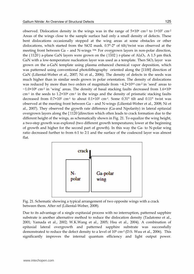
cm-1 in the seeds to 1.2×104 cm-1 in the wings and the density of prismatic stacking faults decreased from 0.7×102 cm-1 to about 0.1×102 cm-1. Some 0.31° tilt and 0.11° twist was observed at the meeting front between Ga – and N-wings (Liliental-Weber et al., 2008; Ni et al., 2007). They observed the growth rate difference (Ga-and Npolarity) in lateral epitaxial overgrown layers along the [ 1120 ]direction which often leads to crack formation due to the different height of the wings, as schematically shown in Fig. 21. To equalize the wing height, a two-step growth was explored (two different growth temperatures; lower at the beginning of growth and higher for the second part of growth). In this way the Ga- to N-polar wing ratio decreased further to from 6:1 to 2:1 and the surface of the coalesced layer was almost flat.
Fig. 21. Schematic showing a typical arrangement of two opposite wings with a crack between them. After ref (Liliental-Weber, 2008).
Due to its advantage of a single expitaxial process with no interruption, patterned sapphire substrate is another alternative method to reduce the dislocation density (Tadatomo et al., 2001; Yamada et al., 2002; W.K.Wang et al., 2005; Hsu et al., 2004). A combination of epitaxial lateral overgrowth and patterned sapphire substrate was successfully demonstrated to reduce the defect density to a level of 105 cm-2 (D.S. Wuu et al., 2006). This significantly improves the internal quantum efficiency and light output power.
www.intechopen.com
Optoelectronics - Materials and Techniques
126
Furthermore, based on the studies by researchers (Tadatomo et al., 2001; Yamada et al., 2002; W.K.Wang et al., 2005; Hsu et al., 2004; Pan et al., 2007; Gao et al., 2008; J. Wang et al., 2006; Kang et al., 2007), the different patterns (shapes or sizes) of the patterned sapphire substrate were found to be able to influence the growth behavior and dislocation distribution of the GaN epilayers. The epitaxial lateral overgrowth growth by hydride vapor phase epitaxy of GaN on patterned metalorganic vapor-phase epitaxy GaN/sapphire and sapphire substrates was investigated by Tourret (Tourret et al., 2008). High-quality uniform GaN films about 10 mm thick were successfully grown after epitaxial lateral overgrowth and coalescence on sapphire substrates.
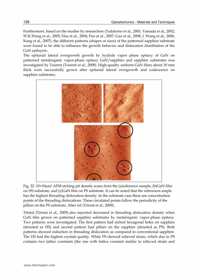
Fig. 22. 10×10µm2 AFM etching pit density scans from the (a)reference sample, (b)GaN film on HS substrate, and (c)GaN film on PS substrate. It can be noted that the references ample has the highest threading dislocation density. In the substrate case there are concentration points of the threading dislocations. These circulated points follow the periodicity of the pillars on the PS substrate. After ref (Törmä et al., 2009).
Törmä (Törmä et al., 2009) also reported decreased in threading dislocation density when GaN film grown on patterned sapphire substrates by metalorganic vapor-phase epitaxy. Two patterns were investigated. The first pattern had etched hexagonal holes on sapphire (denoted as HS) and second pattern had pillars on the sapphire (denoted as PS). Both patterns showed reduction in threading dislocation as compared to conventional sapphire. The HS had the highest crystals quality. While PS showed relieved strain, which due to PS contains two lattice constants (the one with lattice constant similar to relieved strain and
www.intechopen.com
Gallium Nitride: An Overview of Structural Defects
127
other one with lattice constant nearly similar to standard GaN grown on a conventional substrate. Threading dislocation density in PS followed the period of the sapphire pattern and mostly concentrated on top of the pillars. The lesser threading dislocation around the pillars area is possibly caused by the dislocation bending (Hiramatsu et al., 2000; Bougrov et al., 2006) on the inclined facets during GaN growth. Fig. 22 (a), (b) and (c) show the 10×10µm2 AFM etching pit density scans from the GaN surface grown on the conventional substrate, HS and PS substrates, respectively. A similar result was obtained by Dong-Sing Wuu (Wuu et al., 2009). The GaN epilayers on recess/hole -patterned substrate had the highest quality (less defects density) and exhibited a regular distribution of threading dislocation. Table 6 summarizes the structural properties of GaN epilayers on conventional sapphire (flat surface) and patterned sapphire (protruding and recess type) substrates.
FWHM (arcsec)
Dislocation density (cm-2) Sample
(002) (302) Screw-type Edge-type
Etch pit density (cm-2)
Conventional sapphire
224 486 1.0 × 10⁸ 1.6 × 10⁹ 1.4 × 10⁹
Protruding patterned sapphire substrate
245 422 1.2 × 10⁸ 1.2 × 10⁹ 8.2 × 10⁸
Recess patterned sapphire substrate
225 388 1.0 × 10⁸ 1.0 × 10⁹ 6.8 × 10⁸
Table 6. The structural properties of GaN epilayers on conventional sapphire and patterned sapphire. After ref. (Wuu et al., 2009). (FWHM: full width at half maximum)
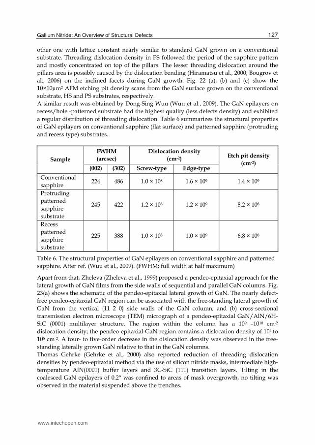
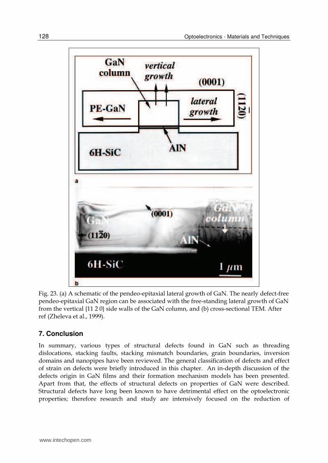
Apart from that, Zheleva (Zheleva et al., 1999) proposed a pendeo-epitaxial approach for the lateral growth of GaN films from the side walls of sequential and parallel GaN columns. Fig. 23(a) shows the schematic of the pendeo-epitaxial lateral growth of GaN. The nearly defect-free pendeo-epitaxial GaN region can be associated with the free-standing lateral growth of GaN from the vertical {11 2 0} side walls of the GaN column, and (b) cross-sectional transmission electron microscope (TEM) micrograph of a pendeo-epitaxial GaN/AlN/6H-SiC (0001) multilayer structure. The region within the column has a 109 –1010 cm-2 dislocation density; the pendeo-epitaxial-GaN region contains a dislocation density of 104 to 105 cm-2. A four- to five-order decrease in the dislocation density was observed in the free-standing laterally grown GaN relative to that in the GaN columns. Thomas Gehrke (Gehrke et al., 2000) also reported reduction of threading dislocation densities by pendeo-epitaxial method via the use of silicon nitride masks, intermediate high-temperature AlN(0001) buffer layers and 3C-SiC (111) transition layers. Tilting in the coalesced GaN epilayers of 0.2° was confined to areas of mask overgrowth, no tilting was observed in the material suspended above the trenches.
www.intechopen.com
Optoelectronics - Materials and Techniques
128
Fig. 23. (a) A schematic of the pendeo-epitaxial lateral growth of GaN. The nearly defect-free pendeo-epitaxial GaN region can be associated with the free-standing lateral growth of GaN from the vertical {11 2 0} side walls of the GaN column, and (b) cross-sectional TEM. After ref (Zheleva et al., 1999).
7. Conclusion
In summary, various types of structural defects found in GaN such as threading dislocations, stacking faults, stacking mismatch boundaries, grain boundaries, inversion domains and nanopipes have been reviewed. The general classification of defects and effect of strain on defects were briefly introduced in this chapter. An in-depth discussion of the defects origin in GaN films and their formation mechanism models has been presented. Apart from that, the effects of structural defects on properties of GaN were described. Structural defects have long been known to have detrimental effect on the optoelectronic properties; therefore research and study are intensively focused on the reduction of
www.intechopen.com
Gallium Nitride: An Overview of Structural Defects
129
structural defects in order to obtain reliable GaN-based devices. In view of this, several different techniques i.e. intermediate temperature layer, nitridation and epitaxial lateral overgrowth that are commonly used to minimize the structural defects in GaN films, have also been compiled and discussed. Generally, the causes of the defects are found to be closely related to substrates, growth conditions, growth techniques and impurities.
8. Acknowledgement
This work was conducted under RU grant (grant no.: 1001/PFIZIK/811155). The support from Universiti Sains Malaysia is gratefully acknowledged.
9. References
Amano, H., Iwaya, M., Hayashi, N., Kashima, T., Katsuragawa, M., Takeuchi, T., Wetzel, C., & Akasaki, I., (1999). MRS Internet J. of Nitride Semicond., Vol. Res. 4S1, No. G10.1 .
Araki, T., Chiba, Y., Nobata, M., Nishioka, Y., & Nanishi, Y., (2000). Structural characterization of GaN grown by hydrogen-assisted ECR-MBE using electron microscopy. J. Crystal Growth, Vol. 209, pp. 368-372.
Barbaray, B., Potin, V., Ruterana, P., & Nouet, G., (1999). Inversion domains generated at substrate steps in GaN/(0001) Al2O3 layers. Diamond and Related Materials, Vol. 8, No. 2-5, pp. 314–318.
Boguslavski, P., Briggs, E.L., & Bernholc, J., (1995). Native defects in gallium nitride. Phys.
Rev. B, Vol. 51, pp. 17255. Boguslavski, P., Brigs, E.L., & Bernholc, J., (1996). Amphoteric properties of substitutional
carbon impurity in GaN and AlN. Appl. Phys. Lett., Vol. 69, pp. 233. Bougrov, V.E., Odnoblyudov, M.A., Romanov, A.E., Lang, T., & Konstantinov, O.V., (2006).
Threading dislocation density reduction in two-stage growth of GaN layers Phys. Status Solidi (a), Vol. 203, No. 4, pp. R25-R27.
Bourret-Courchesne, E.D., Kellermann, S., Yu, K.M., Benamara, M., Liliental-Weber, Z., & Washburn, J., (2000). Reduction of threading dislocation density in GaN using an intermediate temperature interlayer. Appl. Phys. Lett., Vol. 77, No. 22, Pp. 3562.
Bourret-Courchesne, E.D., Yu, K.M., Benamara, M., Liliental-Weber, Z., & Washburn, J., (2001). J. Electron. Mat., Vol. 30, No.11, pp. 1417-1420.
Brown, P.D., (2000). TEM assessment of GaN epitaxial growth. J. Crystal Growth, Vol. 210, pp. 143 – 150.
Chen, Y., Schneider, R., Wang, S.Y., Kem, R.S., Chen, C.H., & Kuo, C.P., (1999). Dislocation reduction in GaN thin films via lateral overgrowth from trenches. Appl. Phys. Lett., Vol. 75, No. 14, pp.2062.
Chien, F. R., Ning, X. J., Stemmer, S., Pirouz, P., Bremser, M. D., & Davis, R. F., (1996). Growth defects in GaN films on 6H–SiC substrates. Appl. Phys. Lett. Vol. 68, pp. 2678.
Cullity, B.D., (1967). Elements of X-Ray Diffraction, Addison-Wesley, United States of America.
Edgar, J. H. (1994). Properties of Group III Nitrides, INSPEC, London, U.K.
www.intechopen.com
Optoelectronics - Materials and Techniques
130
Elsner, J., Jones, R., Haugk, M., Gutierrez, R., Frauenheim, Th., Heggie, M. I., Oberg, S., & Briddon, P. R., (1998). Effect of oxygen on the growth of (100) GaN surfaces: The formation of nanopipes. Appl. Phys. Lett., Vol, 73, pp. 3530.
Fong, W.K., Zhu, C.F., Leung, B.H., & Surya, C., (2000). MRS Internet J. of Nitride Semicond., Vol. Res. 5, No. 12.
Fujii, H., Kisielowski, C., Krüger, J., Leung, M. S. H., Klockenbrink, R., Rubin, M., & Weber, E. R., (1997). Impact of growth temperature, pressure, and strain on the morphology of gan films. III-V Nitrides MRS Proceedings, Vol. 449, pp. 227.
Gao, H., Yan, F., Zhang, Y., Li, J., Zeng, Y., & Wang, G., (2008). Fabrication of nano-patterned sapphire substrates and their application to the improvement of the performance of GaN-based LEDs. J. Phys. D: Appl. Phys., Vol. 41, No. 11, pp. 115106.
Garni, B., Ma, J., Perkins, N., Liu, J., Kuech, T.F., & Lagally, M.G. (1996). Scanning tunneling microscopy and tunneling luminescence of the surface of GaN films grown by vapor phase epitaxy. Appl. Phys. Lett., Vol. 68, No. 10, pp. 1380.
Gehrke, T., Linthicum, K.J., Preble, E., Rajagopal, P., Ronning, C, etl., (2000). Pendeo-epitaxial growth of gallium nitride on silicon substrates. Journal of electronic
materials, Vol. 29, No. 3, pp. 306-310. Gloux, F., Ruterana, P., Lorenz, K., & Alves, E., (2008). A comparative structural
investigation of GaN implanted with rare earth ions at room temperature and 500 °C. Materials Science and Engineering B, Vol. 146, pp. 204–207.
Grandjean, N., Massies, J., & Leroux, M., (1996). Nitridation of sapphire. Effect on the optical properties of GaN epitaxial overlayers. Appl. Phys. Lett., Vol. 69, No. 14, pp. 2071.
Harima, H. (2002). Properties of GaN and related compounds studied by means of Raman scattering. J. Phys.: Condens. Matter, Vol. 14, pp. 967–993.
Henini, M., & Razeghi, M. (April 6, 2005). Optoelectronic Devices: III Nitrides (1st edition), pp. 3, Elsevier Science.
Higashi, G.S., Becker, R.S., Chabal, Y.J., & Becker, A.J., (1991). Comparison of Si(111) surfaces prepared using aqueous solutions of NH4F versus HF. Appl. Phys. Lett., Vol. 58, No. 15, pp. 1656.
Hiramatsu, K., Nishiyamaa, K., Onishia, M., Mizutania, H., Narukawaa, M., Motogaitoa, A., Miyakea, H., Iyechikab, Y., & Maedaet, T., (2000). Fabrication and characterization of low defect density GaN using facet-controlled epitaxial lateral overgrowth (FACELO). J. Crystal Growth, Vol. 221, No. 1-4, pp. 316.
Hong, S. K. & H. K. Cho, (2009). Oxide and Nitride Semiconductors Processing, Properties, and Applications. Advances in Materials Research, Vol. 12, pp. 261-310, DOI 10.1007/978-3-540-88847-5_6
Hsu, Y.P., Chang, S.J., Su, Y.K., Sheu, J.K., Lee, C.T., Wen, T.C., Wu, L.W., Kuo, C.H., Chang, C.S., & Shei, S.C., (2004). Lateral epitaxial patterned sapphire InGaN/GaN MQW LEDs J. Cryst. Growth, Vol. 261, No. 4, pp. 466.
Hull, D., & Bacon, D.J., (1984). Introduction to Dislocations, Pergamon Press, Oxford. Ibach, H., & Lüth, H., (1996). Solid State Physics: An Introduction to Principles of Materials
Science (2nd edition), Springer-Verlag, Berlin Heidelberg, Germany. Iwaya, M., Takeuchi, T., Yamaguchi, S., Wetzel, C., Amano, H., & Akasaki, I., (1998).
Reduction of Etch Pit Density in Organometallic Vapor Phase Epitaxy-Grown GaN
www.intechopen.com
Gallium Nitride: An Overview of Structural Defects
131
on Sapphire by Insertion of a Low-Temperature-Deposited Buffer Layer between High-Temperature-Grown GaN. Jpn. J. Appl. Phys. Vol. 37, pp. L316-L318.
Jenkins, D.W., Dow, J.D., Tsai, & M.-H., (1992). N vacancies in AlxGa1−xN. J. Appl. Phys., Vol. 72, pp. 4130.
Kang, D.H., Song, J.C., Shim, B.Y., Ko, E.A., Kim, D.W., Kannappan, S., & Lee, C.R., (2007). Characteristic Comparison of GaN Grown on Patterned Sapphire Substrates Following Growth Time. Jpn. J. Appl. Phys. Vol. 46, pp. 2563.
Kapolnek, D., Wu, X. H., Heying, B., Keller, B. P., Mishra, U. K., DenBaars, S. P., & Speck, J. S., (1995). Structural evolution in epitaxial metalorganic chemical vapor deposition grown GaN films on sapphire. Appl. Phys. Lett., Vol. 67, pp. 1541.
Kappers, M.J., Datta, R., Oliver, R.A., Rayment, F.D.G., Vickers, M.E., & Humphreys, C.J., (2007). Threading dislocation reduction in (0 0 01) GaN thin films using SiNx interlayers . Journal of Crystal Growth, Vol. 300, No. 1, pp. 70–74.
Keller, S., Keller, B.P., Wu, Y.F., Heying, B., Kapolnek, D., Speck, J.S., Mishra, U.K., & DenBaars, S.P., (1996). Influence of sapphire nitridation on properties of gallium nitride grown by metalorganic chemical vapor deposition. Appl. Phys. Lett., Vol. 68, No. 11, pp. 1525.
Kim, W., Botchkarev, A.E., Salvador, A., Popovici, G., Tang, H., & Morkoc, H., (1997). On the incorporation of Mg and the role of oxygen, silicon, and hydrogen in GaN prepared by reactive molecular beam epitaxy. J. Appl. Phys., Vol. 82, pp. 219.
Kuo, C.W., Fu, Y.K., Kuo, C.H., Chang, L.C., Tun, C.J., Pan, C.J., & Chi , G.C., (2009) Dislocation reduction in GaN with double MgxNy/AlN buffer layer by metal organic chemical vapor deposition. Journal of Crystal Growth, Vol. 311, No. 2, pp. 249–253.
Lee, K., & Auh, K., (2001). MRS Internet J. of Nitride Semicond. Vol. Res. 6, No. 9. Lester, S. D., Ponce, F. A., Crawford, M. G., & Steigerwald, D. A., (1995). High dislocation
densities in high efficiency GaN-based light-emitting diodes. Appl. Phys. Lett., Vol. 66, pp. 1249.
Levinshtein, M.E., Rumyantsev, S.L., & Shur, M.S. (February 21, 2001). Properties of Advanced
Semiconductor Materials: Gan, Aln, Inn , BN , SiC ,SiO2 (1 edition), pp. 1, Wiley-Interscience, New York.
Liliental-Weber, Z., Zakharov, D.N., (2007). Defects formed in nonpolar GaN grown on SiC and Al2O3: Structural perfection of laterally overgrown GaN layers, In: Nitrides
with Nonpolar Surfaces: Growth, Properties and Devices, Paskova, T., (Ed.), Wiley-VCH Verlag.
Liliental-Weber, Z., (2008). TEM studies of GaN layers grown in non-polar direction: Laterally overgrown and pendeo-epitaxial layers. Journal of Crystal Growth, Vol. 310, pp. 4011– 4015.
Liliental-Weber, Z., Ni, X., & Morkoc, H., (2008). Structural perfection of laterally overgrown GaN layers grown in polar- and non-polar directions. J. Mater. Sci.: Mater. Electron.
Vol. 19, No. 8-9, pp. 815-820. Liu, F., Collazo, R., Mita, S., Sitar, Z., Pennycook, S.J., & Duscher. G., (2008). Direct
Observation of Inversion Domain Boundaries of GaN on c-Sapphire at Sub-ångstrom Resolution. Advanced Materials, Vol. 20, No. 11, pp. 2162-2165.
www.intechopen.com
Optoelectronics - Materials and Techniques
132
Liu,L., & Edgar, J.H. (2002). Substrates for gallium nitride epitaxy. Materials Science and
Engineering, Vol. 37, pp. 61–127. Łucznik, B., Pastuszka, B., Kamler, G., Weyher, J.L., Grzegory, I., & Porowski, S., (2009).
Bulk GaN crystals and wafers grown by HVPE without intentional doping. Phys. stat. sol. (c), Vol. 6, No. S2, pp. S297-S300.
Maksimov, O., Fisher, P., Skowronski, M., & Heydemann, V.D., (2006). Effect of nitridation on crystallinity of GaN grown on GaAs by MBE. Materials Chemistry and Physics, Vol. 100, No. 2-3, pp. 457–459.
Marchand, H., Ibbetson, J.P., Kozodoy, P., Keller, S., DenBaars, S., Speck, J.S., & Mishra, U.K., (1998). MRS Internet J. of Nitride Semicond., Vol. Res. 3, No. 3.
Maruska, H.P., & Tietjen, J.J., (1969). The preparation and properties of vapor- deposited single-crystal-line GaN. Appl. Phys. Lett., Vol. 15, pp. 327.
Monemar, B., Bergman, J.P., & Buyanova, I.A., (1997). Optical Characterization of GaN and Related Materials, In: GaN and Related Materials, Pearton, S.J., pp. 85-139, Gordon and Breach Science Publications, The Netherlands.
Morkoc, H., Strite, S., Gao, G. B., Lin, M. E., Sverdlov, B., & Burns, M. (1994). Large-band-gap SiC, III-V nitride, and II-VI ZnSe-based semiconductor device technologies. J. Appl. Phys., Vol. 76, No. 3, pp. 1363.
Morkoc, H., Series Editors, (1999a). Nitride Semiconductor and Devices, Springer- Verlag, ISBN 3-540-64038-x, Berlin, Heidelberg, New York, pp. 11-16.
Morkoc, H., & Series Editors, (1999b). Nitride Semiconductor and Devices, Springer-Verlag, Berlin, Heidelberg, New York, pp. 149
Motoki, K., (2010). Development of Gallium Nitride Substrates. SEI Technical review, No. 70, pp. 28-35.
Nagahama, S., Iwasa, N., Senoh, M., Matsushita, T., Sugimoto, Y., Kiyoku, H., Kozaki, T., Sano, M., Matsumura, H., Umemoto, H., Chocho, K., & Mukai, T., (2000). High-Power and Long-Lifetime InGaN Multi-Quantum-Well Laser Diodes Grown on Low-Dislocation-Density GaN Substrates. Jpn. J. Appl. Phys., Vol. 39, pp. L647-650.
Nakamura, S., & Chichibu, S.F (2000). Introduction, In: Introduction to nitride semiconductor
blue lasers and light emitting diodes, Taylor & Francis, London, New York. Namkoong, G., Doolittle, W.A., Sa, H., Brown, A.S., Stock, S.R., (2000). MRS Internet J. of
Nitride Semicond., Vol. Res. 5, No. 10. Namkoong, G., Doolittle, W.A., Brown, A.S., Losurdo, M., Capezzuto, P., & Bruno, G.,
(2002). Role of sapphire nitridation temperature on GaN growth by plasma assisted molecular beam epitaxy: Part I. Impact of the nitridation chemistry on material characteristics. J. Appl. Phys., Vol. 91, No. 4, pp. 2499.
Neugebauer, J., & Van de Walle, C.G., (1994). Atomic geometry and electronic structure of native defects in GaN. Phys. Rev. B, Vol. 50, pp. 8067.
Neugebauer, J., & Van de Walle, C.G., (1996). Gallium vacancies and the yellow luminescence in GaN. Appl. Phys. Lett., Vol. 69, No. 4, pp. 503.
Ng, T. B., Han, J., Biefeld, R. M., & Weckwerth, M. V. (1998). In-situ reflectance monitoring during MOCVD of AlGaN. J. Electron. Mat., Vol. 27, pp. 190.
www.intechopen.com
Gallium Nitride: An Overview of Structural Defects
133
Ni, X., Özgür, U., Fu, Y., Biyikli, N., Xie, J., Baski, A.A., Morkoç, H., & Liliental-Weber, Z., (2006). Defect reduction in (110) a-plane GaN by two-stage epitaxial lateral overgrowth. Appl. Phys. Lett., Vol. 89, No. 26, pp. 262105.
Ni, X., Ozgur, U., Morkoc, H., Liliental-Weber, Z., & Everitt, H.O., (2007). Epitaxial lateral overgrowth of a-plane GaN by metalorganic chemical vapor deposition. J. Appl.
Phys., Vol. 102, No. 5, pp. 53506. Northrup, J.E., (1998). Theory of the (1210) prismatic stacking fault in GaN. Appl. Phys. Lett.,
Vol. 72, pp. 2316. Ohtani, A., Stevens, K. S., & Beresford, R., (1994). Growth and characterization of Gan on
Si(111). Diamond, SiC and Nitride Wide Bandgap Semiconductors MRS Proceedings,Vol. 339, pp. 471-476.
Pan, C.C., Hsieh, C.H., Lin, C.W., & Chyi, J.I., (2007). Light output improvement of InGaN ultraviolet light-emitting diodes by using wet-etched stripe-patterned sapphire substrates. J. Appl. Phys., Vol. 102, No. 8, pp. 84503.
Pearton, S.J., (1997a). Volume 2- GaN and Related Materials, In: Optoelectronic properties of
semiconductors and superlattices, Manasreh, M.O., & Series editors, pp. 149, Gordon and Breach Science Publishers, Amsterdam.
Pearton, S.J., (1997b). Volume 2- GaN and Related Materials, In: Optoelectronic properties of
semiconductors and superlattices, Manasreh, M.O., & Series editors, pp. 96-98, Gordon and Breach Science Publishers, Amsterdam.
Pearton, S.J., (2000). Volume 7- GaN and Related Materials II, In: Optoelectronic properties of
semiconductors and superlattices, Manasreh, M.O., & Series editors, pp. 134, Gordon and Breach Science Publishers, Amsterdam.
Perlin, P., Suzuki, T., Teisseyre, H., Leszczynski, M., Grezgory, I., Jun, J., Porowski, S., Boguslavski, P., Bernholc, J., Chervin, J.C., Polian, A., & Moustakas, T.D., (1995). Towards the Identification of the Dominant Donor in GaN. Phys. Rev. Lett., Vol. 75, pp. 296.
Ponce, F.A., Bour, D. P., Götz, W., & Wright, P.J., (1996). Spatial distribution of the luminescence in GaN thin films. Appl. Phys. Lett., Vol. 68, No. 1, pp. 57.
Ponce, F.A., Young, W.T., Cherns, D., Steeds, J.W., & Nakamura, S., (1997). Nanopipes and inversion domains in high quality gan epitaxial layers. III-V Nitrides MRS Proceedings, Vol. 449, pp. 405
Powell, R.C., Tomasch, G.A., Kim, Y.W., Thornton, J.A., & Greene, J.E., (1990) Growth of high-resistivity wurtzite and zincblende structure single crystal Gan by reactive-ion molecular beam epitaxy. Diamond, Boron Nitride, Silicon Carbide and Related Wide Bandgap Semiconductors
MRS Proceedings, Vol. 162, pp. 525. Qian, W., Rohrer, G.S., Skowronski, M., Doverspike, K., Rowland, L.B., & Gaskill, D.K.,
(1995b). Open-core screw dislocations in GaN epilayers observed by scanning force microscopy and high-resolution transmission electron microscopy. Appl. Phys. Lett., Vol. 67, pp. 2284.
Qian, W., Skowronski, M., De Graef, M., Doverspike, K., Rowland, L. B., & Gaskill, D. K., (1995a). Microstructural characterization of ┙-GaN films grown on sapphire by organometallic vapor phase epitaxy. Appl. Phys. Lett., Vol. 66, pp. 1252.
www.intechopen.com
Optoelectronics - Materials and Techniques
134
Romano, L.T., Northrup, J.E., & O’Keefe, M. A., (1996). Inversion domains in GaN grown on sapphire. Appl. Phys. Lett. Vol. 69, pp. 2394.
Romano, L.T., & Myers, T.H., (1997). The influence of inversion domains on surface morphology in GaN grown by molecular beam epitaxy. Appl. Phys. Lett., Vol. 71, pp. 3486.
Sakai, A., Sunakawa, H., & Usui, A., (1997). Defect structure in selectively grown GaN films with low threading dislocation density. Appl. Phys. Lett., Vol. 71, No. 16, pp. 2259.
Sakai, S., Wang, T., Morishima, Y., & Naoi, Y., (2000). A new method of reducing dislocation density in GaN layer grown on sapphire substrate by MOVPE J. Crystal Growth, Vol. 221, No. 1-4, pp. 334.
Sa´nchez, A.M., Pacheco, F.J., Molina, S.I., Ruterana, P., Calle, F., Palacios, T.A., Sa´nchez-Garcı´a, M.A., Calleja, E., & Garcı´a,R., (2002). AlN buffer layer thickness influence on inversion domains in GaN/AlN/Si(111). Materials Science and Engineering B, Vol. 93, pp. 181-184.
Sawadaishi, M., Taguchi, S., Sasaya, K., & Honda, T., (2009). Nitridation of (1 1 1) Al substrates for GaN growth by molecular beam epitaxy . Journal of Crystal Growth, Vol. 311, No. 7, pp. 1994–1996.
Sitar, Z., Paisley, M.J., Yan, B., & Davis, R.F., (1990). Structural defects in gan epilayers grown by gas source molecular beam epitaxy, Diamond, Boron Nitride, Silicon Carbide and Related Wide Bandgap Semiconductors
MRS Proceedings, Vol. 162, pp. 537. Smith, D.J., Chandrasekhar, D., Sverdlov, B., Botchkarev, A., Salvador, A., & Morkoc, H.,
(1995). Characterization of structural defects in wurtzite GaN grown on 6H SiC using plasma-enhanced molecular beam epitaxy. Appl. Phys. Lett., Vol. 67, pp. 1830.
Smith, W.F., (1996). Principles of Materials Science and Engineering (3rd edition), pp. 141, McGraw-Hill, New York.
Spitsyn, B.V., Popovici, G., & Prelas, M.A. (1993). 2nd Int. Conf. On the Applications of Diamond Films and Related Materials, edited by Yoshikawa, M., MY, Tokyo.
Stradling, R.A., & Klipstein, P.C., (1991). Growth and Characterization of Semiconductors, Adam Hilger, New York.
Sverdlov, B.N., Martin, G. A., Morkoc, H., & Smith, D.J., Formation of threading defects in GaN wurtzite films grown on nonisomorphic substrates. Appl. Phys. Lett., Vol. 67, pp. 2063.
Tadatomo, K., Okagawa, H., Ohuchi, Y., Tsunekawa, T., Imada, Y., Kato, M., & Taguchi, T., (2001). High Output Power InGaN Ultraviolet Light-Emitting Diodes Fabricated on Patterned Substrates Using Metalorganic Vapor Phase Epitaxy. Jpn. J. Appl. Phys. Vol. 40, pp. L583.
Tempel, A., Seifert, W., Hammer, J., & Butter, E., (1975). Krist. Technol., Vol.747. Törmä, P.T., Ali, M., Svensk, O., Sintonen, S., Kostamo, P., Suihkonen, S., Sopanen, M.,
Lipsanen, H., Odnoblyudov, M.A., & Bougrov, V.E., (2009). An investigation of structural properties of GaN films grown on patterned sapphire substrates by MOVPE. Physica B : Condensed Matter, 404 (2009) 4911–4915 .
www.intechopen.com
Gallium Nitride: An Overview of Structural Defects
135
Tourret, J., Gourmala, O., Trassoudaine, A., Andre, Y., Gil, E., Castelluci, D., & Cadoret, R., (2008). Low-cost high-quality GaN by one step growth .Journal of Crystal Growth, Vol. 310, No. 5, pp. 924-929.
Usui, A., Sunakawa, H., Sakai, A., & Yamaguchi, A.A., (1997). Thick GaN Epitaxial Growth with Low Dislocation Density by Hydride Vapor Phase Epitaxy. Japn. J. Appl. Phys., Vol. 36, pp. L899.
Valcheva, E., Paskova, T., Persson, P.O.Å., & Monemar, B., (2002). Nanopipes in Thick GaN Films Grown at High Growth Rate. Phys. stat. sol. (a), Vol. 194, No. 2, pp. 532–535.
Wang, J., Guo, L.W., Jia, H.Q., Xing, Z.G., Wang, Y., Yan, J.F., Yu, N.S., Chen, H., & Zhou, J.M., (2006). Investigation of characteristics of laterally overgrown GaN on striped sapphire substrates patterned by wet chemical etching. J. Cryst. Growth, Vol. 290, No. 2, pp. 398
Wang, W.K., Wuu, D.S., Lin, S.H., Han, P., Horng, R.H., Hsu, T.C., Huo, D.T.C. , Jou, M.J., Yu, Y.H., & Lin, A., (2005). Efficiency improvement of near-ultraviolet InGaN LEDs using patterned sapphire substrates. IEEE J. Quantum Electron, Vol. 41, No. 11, pp. 1403.
Weyher, J.L., Brown, P.D., Zauner, A.R.A., Muller, S., Boothroyd, C.B., Foord, D.T., Hageman, P.R., Humphreys, C.J., Larsen, P.K., Grzegory, I., & Porowski, S. (1999). Morphological and structural characteristics of homoepitaxial GaN grown by metalorganic chemical vapour deposition (MOCVD). J. Crystal Growth, Vol. 204, pp. 419-428.
Weyher, J.L., Łucznik, B., Grzegory, I., Smalc-Koziorowska, J., & Paskova, T., (2010). Revealing of extended defects in HVPE-grown GaN, Journal of Crystal Growth, Vol. 312, pp. 2611-2615.
Wong, Y.Y., Chang, E.Y., Yang, T.H., Chang, J.R., Chen, Y.C., Ku, J.T., Lee, C.T., & Chang, C.W., (2009). The effect of AlN buffer growth parameters on the defect structure of GaN grown on sapphire by plasma-assisted molecular beam epitaxy. Journal of
Crystal Growth, Vol. 311, No. 6, pp. 1487–1492. Wuu, D.S., Wang, W.K., Wen, K.S., Huang, S.C., Lin, S.H., Huang, S.Y., Lin, C.F., Horng,
R.H., (2006). Defect reduction and efficiency improvement of near-ultraviolet emitters via laterally overgrown GaN on a GaN/patterned sapphire template Appl.
Phys. Lett., Vol. 89, No. 16, pp. 161105. Wuu, D.S., Wu, H.W., Chen, S.T., Tsai, T.Y., Zheng, X., & Horng, R.H., (2009). Defect
reduction of laterally regrown GaN on GaN/patterned sapphire substrates. Journal
of Crystal Growth, Vol. 311, No. 10, pp. 3063–3066. Xu, H.Z., Takahashi, K., Wang, Z.G., Wang, C.X., Okada, Y., Kawabe, M., Harrison, I., &
Foxon, C.T., (2001). Effect of in situ thermal treatment during growth on crystal quality of GaN epilayer grown on sapphire substrate by MOVPE. J. Crystal Growth, Vol. 222, pp. 110-117.
Yamada, M., Mitani, T., Narukawa, Y., Shioji, S., Niki, I., Sonobe, S., Deguchi, K., Sano, M., & Mukai, T., (2002). InGaN-Based Near-Ultraviolet and Blue-Light-Emitting Diodes with High External Quantum Efficiency Using a Patterned Sapphire Substrate and a Mesh Electrode. Jpn. J. Appl. Phys., Vol.41, pp. L1431-L1433.
www.intechopen.com
Optoelectronics - Materials and Techniques
136
Yokouchi, K., Araki, T., Nagatomo, T., & Omoto, O., (1996). Epitaxial growth of GaN films on silicon substrates by MOVPE. Inst. Phys. Phys. Conf. Ser., Vol. 142, pp. 867.
Zakharov, D.N., Liliental-Weber, Z., Wagner, B. Reitmeier, Z.J., Preble, E.A., & Davis, R.F, (2005). Structural TEM study of nonpolar a-plane gallium nitride grown on (112� 0) 4H-SiC by organometallic vapor phase epitaxy. Phys. Rev. B, Vol. 71, pp. 235334.
Zhang, X., Li, R.R., Dapkus, P.D., & Rich, D.H., (2000). Direct lateral epitaxy overgrowth of GaN on sapphire substrates based on a sparse GaN nucleation technique. Appl.
Phys. Lett., Vol. 77, No. 14, pp. 2213. Zheleva, T.S., Smith, S.A., Thomson, D.B., Linthicum, K.J., Rajagopal, P., & Davis, R.F.,
(1999). Pendeo-epitaxy: A new approach for lateral growth of gallium nitride films.
Journal of Electronic materials, Vol.28, No.4, pp. L8-L5.
www.intechopen.com
Optoelectronics - Materials and TechniquesEdited by Prof. P. Predeep
ISBN 978-953-307-276-0Hard cover, 484 pagesPublisher InTechPublished online 26, September, 2011Published in print edition September, 2011
InTech EuropeUniversity Campus STeP Ri Slavka Krautzeka 83/A 51000 Rijeka, Croatia Phone: +385 (51) 770 447 Fax: +385 (51) 686 166www.intechopen.com
InTech ChinaUnit 405, Office Block, Hotel Equatorial Shanghai No.65, Yan An Road (West), Shanghai, 200040, China
Phone: +86-21-62489820 Fax: +86-21-62489821
Optoelectronics - Materials and Techniques is the first part of an edited anthology on the multifaceted areas ofoptoelectronics by a selected group of authors including promising novices to the experts in the field.Photonics and optoelectronics are making an impact multiple times the semiconductor revolution made on thequality of our life. In telecommunication, entertainment devices, computational techniques, clean energyharvesting, medical instrumentation, materials and device characterization and scores of other areas of R&Dthe science of optics and electronics get coupled by fine technology advances to make incredibly large strides.The technology of light has advanced to a stage where disciplines sans boundaries are finding itindispensable. Smart materials and devices are fast emerging and being tested and applications developed inan unimaginable pace and speed. Here has been made an attempt to capture some of the materials andtechniques and underlying physical and technical phenomena that make such developments possible throughsome real time players in the field contributing their work and this is sure to make this collection of essaysextremely useful to students and other stake holders such as researchers and materials scientists in the areaof optoelectronics.
How to referenceIn order to correctly reference this scholarly work, feel free to copy and paste the following:
Fong Kwong Yam, Li Li Low, Sue Ann Oh, and Zainuriah Hassan (2011). Gallium Nitride: An Overview ofStructural Defects, Optoelectronics - Materials and Techniques, Prof. P. Predeep (Ed.), ISBN: 978-953-307-276-0, InTech, Available from: http://www.intechopen.com/books/optoelectronics-materials-and-techniques/gallium-nitride-an-overview-of-structural-defects

© 2011 The Author(s). Licensee IntechOpen. This chapter is distributedunder the terms of the Creative Commons Attribution-NonCommercial-ShareAlike-3.0 License, which permits use, distribution and reproduction fornon-commercial purposes, provided the original is properly cited andderivative works building on this content are distributed under the samelicense.