“Growth and Characterization of Aluminum Gallium Nitride...
177
UNIVERSITY OF CALIFORNIA Santa Barbara “Growth and Characterization of Aluminum Gallium Nitride/ Gallium Nitride Ultraviolet Detectors” A dissertation submitted in partial satisfaction of the requirements for the degree of Doctor of Philosophy in Electrical and Computer Engineering by Giacinta Parish Committee in charge: Professor Umesh K. Mishra, Chairperson Professor Steven P. DenBaars Doctor James P. Ibbetson Professor Brett D. Nener Professor James S. Speck March 2001
Transcript of “Growth and Characterization of Aluminum Gallium Nitride...

UNIVERSITY OF CALIFORNIA Santa Barbara
“Growth and Characterization of Aluminum Gallium Nitride/ Gallium Nitride Ultraviolet Detectors”
A dissertation submitted in partial satisfaction
of the requirements for the degree of
Doctor of Philosophy
in
Electrical and Computer Engineering
by
Giacinta Parish
Committee in charge:
Professor Umesh K. Mishra, Chairperson
Professor Steven P. DenBaars
Doctor James P. Ibbetson
Professor Brett D. Nener
Professor James S. Speck
March 2001

ii
The dissertation of Giacinta Parish is approved
Committee Chairperson
March 2001

iii
March 2001
Copyright by
Giacinta Parish
2001

iv
Acknowledgments
The opportunity to be at one of the foremost research universities in the world for
GaN research is one I will always be grateful for, and there are many people who
inspired, guided and assisted me. I want to thank my adviser Umesh Mishra for
accepting me to be one of his students. Thank you for all your support and guidance
during my time at UCSB. It has been both an educational and enjoyable experience
to work in the Mishra Group at UCSB. This was reinforced by the fantastic
collaborative atmosphere and the many talented people in the extended solid-state
research community at UCSB.
The members of my defense committee all had constructive and helpful advice and
information for me. As head of the MOCVD lab Steve DenBaars had constant
contact and input into my work in GaN and AlGaN growth. I benefited greatly from
the insights and suggestions of James Ibbetson, both while he was also working in
the MOCVD lab at UCSB, and when he moved to Cree Lighting. I am very grateful
to Jim Speck for his knowledge of and assistance in materials characterization. And,
although Brett Nener was on the other side of the world at the University of Western
Australia, emails, phone calls and several visits to UCSB ensured he was also a
constant source of support and help.
To Stacia Keller I owe more gratitude than I can express, for teaching me so much
about MOCVD, and for the extent of research into AlGaN growth that we
accomplished together.
I�m also glad to have shared the experience with my fellow students in the Mishra
Group. To Can Zheng, Dan Green, DJ Jena, Huili Xing, James Champlain, Jeff Yen,
Lee McCarthy, Likun Shen, Naiqian Zhang, Peter Kozodoy, Prashant Chavarkar,
Primit Parikh, Rama Vetury, Rob Coffie, Rob Underwood, Sten Heikman, Tim
Wisleder and Yifeng Wu � thank you all for your companionship and your
collaboration. And to the members of the York Group who shared our office � Amit
Nagra, Bruce Liu, Jane Xu, Nick Cheng, Paolo Maccarini, Pengcheng Jia, and Vicki
Chen � I offer the same thanks. Similarly to the many students and researchers in
the MOCVD group who I have shared with, been helped by, and learned from all

v
these years � Amber Abare, Andreas Stonas, Beck Mason, Bernd Keller, Brendan
Moran, Dave Kapolnek, Greg Fish, Hugues Marchand, Mike Craven, Mike Mack,
Monica Hansen, Patrick Abraham, Paul Fini, Tal Margalith and Tom Katona� thank
you all. To the gang at The University of Western Australia I am also indebted. They
got me to UCSB, they helped me along the way with offshore advice, simulations,
and data, and they brought me home: thank you Laurie Faraone, John Dell, Charlie
Musca, Joe Jin Kuek, Sabine Betts, Dave Pulfrey at UBC, and all the rest of the
crew. There are many others who have made the journey to this point possible with
their support and assistance. In the MOCVD lab it was Brian Carralejo, and in the
cleanroom Jack Whaley, Bob Hill and Mike Anzlowar, all of you have my unending
gratitude. For administrative support and so much more � thank you Cathy Fogarty,
Lee Baboolal, Joann Erving and Val De Veyra. And thanks to the guys in the
electrical engineering workshop - Bob Stevenson, Avery Juan and Raul Ramirez. I
wish to especially thank Eric Tarsa at Cree Lighting for his important input into this
work with the design of the solar-blind detector. I am also grateful to Lifan Chen for
TEM measurements, to Professor Joe Campbell and his student Charles Collins at
UT Austin for the final responsivity measurements, and to Siegfried Fleischer for his
invaluable help in creating the spectral and temporal response measurement setups.
To Jason my dear darling supportive husband: I don�t know what it would have been
like doing this without you. You always believed in me, even more than I did. Thank
you for your patience, love and endless encouragement. To mum and dad the same
is true. Your support has made a huge difference in reaching this point and I will
always be grateful. And to all my and Jason�s family and friends � thank you all.
Finally I would like to acknowledge the financial support from the Office of Naval
Research and the Air Force Office of Scientific Research that made this work
possible. I would also like to acknowledge the fellowships that enabled me to attend
UCSB - the Fulbright fellowship from the Australian-American Fulbright Association
and the Hackett Scholarship from the University of Western Australia.
vi
Vita
June 29, 1972 Born (Giacinta Matassa) ― Perth, Australia
March 1995 B. Eng., Electronic. ― The University of Western Australia
March 1995 B. Sc., Chemistry ― The University of Western Australia
1995-96 Teaching Assistant ― Department of Electrical and Electronic
Engineering, The University of Western Australia
March 1997 M. Eng. Sc. ― The University of Western Australia
1996-2000 Research Assistant ― Department of Electrical and Computer
Engineering, University of California, Santa Barbara
Publications
1. D.L. Pulfrey, J.J. Kuek, M.P. Leslie, B.D. Nener, G. Parish, U.K. Mishra, P.
Kozodoy and E.J. Tarsa, "High UV/solar rejection ratios in GaN/AlGaN/GaN
p-i-n photodiodes" IEEE Trans. on Electron Device. 48(3) 100-2 (2001).
2. G. Parish, M. Hansen, B. Moran, S. Keller, S.P. DenBaars and U.K. Mishra,
�AlGaN/GaN solar-blind ultraviolet photodiodes on SiC substrate� Proc. IEEE
CORNELL Ithaca, USA, 215-24 (2000).
3. S. Keller, G. Parish, J.S. Speck, S.P. DenBaars and U.K. Mishra, "Dislocation
reduction in GaN films through selective island growth of InGaN" Appl. Phys.
Lett., 77(17), 2665-7 (2000). J. Appl. Phys 87(8) 3900-4 (2000)
4. N.Q. Zhang, S. Keller, G. Parish, S. Heikman, S.P. Denbaars and U.K. Mishra,
"High breakdown GaN HEMT with overlapping gate structure" IEEE Electron
Device Lett. 21(9) 373-5 (2000)
vii
5. E. J. Tarsa, P. Kozodoy, J. Ibbetson, B. P. Keller, G. Parish and U. K. Mishra,
�Solar-blind AlGaN-based inverted heterostructure photodiodes� Appl. Phys.
Lett., 77(3), 316-8 (2000).
6. G.A. Umana-Membreno, J.M. Dell, Y.-F. Wu, G. Parish and U.K. Mishra,
"Anomalous drain current-voltage characteristics in AlGaN/GaN MODFETs at low
temperatures" Microelectronics Journal 31(7) 531-6 (2000)
7. J. Antoszewski, M. Gracey, J.M. Dell, L. Faraone, T.A. Fisher, G. Parish, Y.-F.
Wu and U.K. Mishra, "Scattering mechanisms limiting two-dimensional electron
gas mobility in Al0.25Ga0.75N/GaN modulation-doped field-effect transistors" J.
Appl. Phys 87(8) 3900-4 (2000).
8. G. Parish, S. Keller, S. P. DenBaars and U. K. Mishra, �SIMS Investigations into
the effect of growth conditions on residual impurity and silicon incorporation in
GaN and AlxGa1-xN� J. Electron. Mater. 29(1), 15-20 (2000).
9. D. L. Pulfrey, J. J. Kuek, B. D. Nener, G. Parish, U. K. Mishra, E. J. Tarsa
�Towards an AlGaN, solar-blind, p-i-n photodetector� Phys, Stat. Sol. (A) 176,
169-73 (1999)
10. S, Keller, G. Parish, P. T. Fini, S. Heikman, C.-H. Chen, N. Zhang, S. P.
DenBaars and U. K. Mishra, �Metalorganic chemical vapor deposition of high
mobility AlGaN/GaN heterostructures� J. Appl. Phys. 86(10), 5850-7 (1999).
11. G. Parish, S. Keller, P. Kozodoy, J. P. Ibbetson, H. Marchand, P. T. Fini, S.B.
Fleischer, S. P. DenBaars, U. K. Mishra and E.J. Tarsa, �High-performance
(Al,Ga)N-based solar-blind ultraviolet p-i-n detectors on laterally epitaxially
overgrown GaN� Appl. Phys. Lett. 75(2), 247-9 (1999).
12. C.-H. Chen, K. Krishnamurthy, S. Keller, G. Parish, M. Rodwell, U. K. Mishra and
Y.-F. Wu, �AlGaN/GaN dual-gate modulation-doped field-effect transistors�
Electron. Lett. 35(11), 933-4 (1999).
viii
13. J. J. Xu, Y.-F. Wu, S. Keller, G. Parish, S. Heikman, B. J. Thibeault, U. K. Mishra
and R. A. York, �1-8-GHz GaN-based power amplifier using flip-chip bonding�
IEEE Microwave Guided Wave Lett. 9(7), 280-1 (1999).
14. G.A. Umana-Membreno, J.M. Dell, L. Faraone, Y.-F. Wu, G. Parish and U.K.
Mishra, "Anomalous drain current-voltage characteristics in AlGaN/GaN
MODFETs at low temperatures" Proc. SPIE 3893 454-60 (1999).
15. G. Parish, S. Keller, P. Kozodoy, J. P. Ibbetson, H. Marchand, P. T. Fini, S.B.
Fleischer, S. P. DenBaars, U. K. Mishra and E.J. Tarsa, �Low dark current p-i-n
(Al,Ga)N-based solar-blind UV detectors on laterally epitaxially overgrown GaN�
Proc. IEEE COMMAD Perth, Australia, 175-8 (1998).
16. G. Parish, S. Keller, P. T. Fini, R. Vetury, C.-H. Chen, S. P. DenBaars, U. K.
Mishra and Y.-F. Wu, �MOCVD growth and properties of thin AlxGa1-xN layers on
GaN� Proc. IEEE COMMAD Perth, Australia, 478-81 (1998).
17. G. A. Umana-Membreno, J. M. Dell, B. D. Nener, L. Faraone, G. Parish, Y.-F.
Wu and U. K. Mishra, �Low temperature shallow-trap related output-admittance
frequency dispersion in AlGaN/GaN MODFETs� Proc. IEEE COMMAD Perth,
Australia, 252-5 (1998).
18. J. Antoszewski, M. Gracey, J. M. Dell, L. Faraone, G. Parish, Y.-F. Wu and U. K.
Mishra, �Magneto-transport studies in AlGaN/GaN MODFETs� Proc. IEEE
COMMAD Perth, Australia, 256-9 (1998).
19. C.-H. Chen, S. Keller, G. Parish, R. Vetury, P. Kozodoy, E. L. Hu, S. P.
DenBaars, U. K. Mishra and Y.-F. Wu, �High-transconductance self-aligned
AlGaN/GaN modulation-doped field-effect transistors with regrown ohmic
contacts� Appl. Phys. Lett. 73(21), 3147-9 (1998).
20. R. Vetury, H. Marchand, G. Parish, P. T. Fini, J.P. Ibbetson, S. Keller, J. S.
Speck, S. P. DenBaars and U. K. Mishra, �First demonstration of AlGaN/GaN
heterostructure field effect transistor on GaN grown by lateral epitaxial
ix
overgrowth (LEO).� Proc. 25th Intl. Symp. Compound Semicond. Nara, Japan
177-83 (1998).
21. R. Vetury, Y.-F. Wu, P. T. Fini, G. Parish, S. Keller, S. P. DenBaars and U. K.
Mishra, �Direct measurement of gate depletion in high breakdown (405V)
AlGaN/GaN heterostructure field effect transistors� Proc IEEE IEDM San
Francisco, USA 55-8 (1998).
22. C. A. Musca, J. F. Siliquini, G. Parish, J. M. Dell and L. Faraone, �A monolithic
dual-band HgCdTe infrared detector� J. Cryst. Growth 184-185, 1284-7 (1998)
23. G. Parish, �Development of a monolithic dual-band HgCdTe infrared detector
structure�, Unpublished M. Eng. Sc. Thesis, (1997) The University of Western
Australia, Perth, Australia.
24. G. Parish, C. A. Musca, J. F. Siliquini, J. Antoszewski, J. M. Dell, B. D. Nener, L.
Faraone and G. J. Gouws, �A monolithic dual-band HgCdTe infrared detector
structure� IEEE Electron Device Lett. 18(7), 352-4 (1997)
25. G. Parish, C. A. Musca, J. F. Siliquini, J. Antoszewski, J. M. Dell, B. D. Nener, L.
Faraone and G. J. Gouws, �Fabrication and modelling of a prototype dual-band
HgCdTe infrared detector structure� Proc. IEEE COMMAD Canberra, Australia,
46-9 (1996).
x
Abstract
Growth and Characterization of Aluminum Gallium Nitride/Gallium Nitride for
Ultraviolet Detectors
by Giacinta Parish
There are many areas of potential utilization of the alloy AlxGa1-xN, not the least of
which are ultraviolet detector applications. These include flame and heat sensors,
missile plume detection, and secure-from-earth inter-satellite communications. The
AlxGa1-xN bandgap can be tailored from 4.3eV (xAl=0) to 6.2eV (xAl=1), corresponding
to a band-edge wavelength range of 365nm to 200nm, to suit each unique
application. Solar radiation below approximately 300nm wavelength is absorbed by
ozone in the atmosphere. Thus, for applications in the presence of a large solar
radiation background, a solar-blind detector that exhibits no spectral response for
wavelengths at or above 300nm is extremely desirable. For solar-blind detectors a
composition of greater than 30% Al is needed.
The first phase of this work involved the optimization of metalorganic chemical vapor
deposition epitaxial growth of AlxGa1-xN (xAl ≥ 0.3) on GaN templates. It was found
that defect formation in the AlxGa1-xN is exacerbated as xAl is raised. This could be
partially counteracted by maximizing the mobility of Al surface species during growth,
and by reducing threading dislocation density in the GaN template.
xi
The second phase of the work examined the effect of defects on GaN-based p-i-n
photodiodes. The presence of threading dislocations (especially mixed-character
dislocations) was found to increase the leakage current, broaden the spectral
response, and lengthen the response decay time. Defects in the i-layer, most likely
point defects, were another source of leakage current. The sidewalls did not
contribute to leakage current.
The final phase of the project was the development of bulk AlGaN growth on SiC
substrates for use in solar-blind UV detectors. A nucleation layer or ramped growth
rate was required to avoid cracking due to tensile strain. Si-doping of the n-type
buffer introduced further tension in the film. The threading dislocation density in the
AlGaN grown on SiC was very high � 2-5x1010 cm-2 � much higher than for GaN.
Because the threading dislocations were primarily edge-type, reasonably low diode
leakage currents could still be obtained. An insulating buffer was required to
suppress photocurrent contributions from the SiC substrate. Solar-blind p-GaN/
i-AlGaN/n-AlGaN photodiodes with a peak responsivity of 0.08 A/W were fabricated.
xii
Table of contents
Chapter 1. Introduction ......................................................................................... 1 1.1 Defects � dislocations (extended defects) and point defects ........................... 2
1.1.1 Substrates................................................................................................................ 2 1.1.2 Impurities and doping .............................................................................................. 4
1.2 AlGaN-based devices ..................................................................................... 6 1.3 (Al)GaN photodetectors .................................................................................. 7
1.3.1 Photodetectors......................................................................................................... 9 1.3.2 What is solar-blind operation? ............................................................................... 14 1.3.3. Visible-blind GaN-based detectors ....................................................................... 16 1.3.4. Solar-blind AlGaN-based detectors ...................................................................... 17
1.4 Synopsis of this thesis................................................................................... 18 1.4.1 Chapter 2 ............................................................................................................... 18 1.4.2 Chapter 3 ............................................................................................................... 19 1.4.3 Chapter 4 ............................................................................................................... 20
1.5 References ................................................................................................... 20 Chapter 2. AlGaN growth using sapphire substrate.......................................... 28
2.1 Introduction ................................................................................................... 28 2.1.1 Epitaxially grown bulk AlGaN................................................................................. 28 2.1.2 AlGaN/GaN heterostructures................................................................................. 30 2.1.3 Synopsis of the chapter ......................................................................................... 30
2.2 MOCVD Growth at UCSB ............................................................................. 31 2.2.1 Al incorporation...................................................................................................... 32 2.2.2 Bulk AlGaN growth on sapphire............................................................................. 36 2.2.3 AlGaN/GaN heterostructures................................................................................. 37 2.2.4 LEO growth technique ........................................................................................... 38
2.3 Surface morphology of AlGaN/GaN heterostructures.................................... 39 2.3.1 Effect of xAl ............................................................................................................. 39 2.3.2 Effect of growth conditions..................................................................................... 41 2.3.3 Effect of underlying GaN template......................................................................... 42
2.4. Electrical properties of AlGaN/GaN heterostructures ................................... 43 2.4.1 Effect of xAl ............................................................................................................. 44 2.4.2 Effect of growth conditions..................................................................................... 46
2.5 Impurity incorporation during AlxGa1-xN growth.............................................. 46 2.5.1 Effect of growth conditions..................................................................................... 47 2.5.2 Effect of xAl ............................................................................................................. 52 2.5.3 Si incorporation...................................................................................................... 54
xiii
2.6 Conclusions .................................................................................................. 56 2.7 References ................................................................................................... 57
Chapter 3. Dislocations in GaN and their effect on p-i-n photodetectors. ....... 62 3.1 Defects present in (Al)GaN ........................................................................... 62
3.1.1 General crystal defect theory................................................................................ 62 3.1.2. Dislocation reduction techniques for GaN ............................................................ 65 3.1.3 Effects of defects on (Al)GaN photodetectors ....................................................... 66 3.1.4 Synopsis of this chapter......................................................................................... 69 3.1.5 Mechanisms of p-i-n photodiodes......................................................................... 70 3.1.6 Device layout, processing and measurements...................................................... 72
3.2 Threading dislocation reduction � effect on GaN p-i-n photodiodes............... 76 3.2.1 XRD as a tool for TDD comparison ....................................................................... 77 3.2.2 SiN/InGaN interlayer technique for TDD reduction................................................ 78 3.2.3 GaN templates on SiC substrate ........................................................................... 80 3.2.4 TDD comparison (by XRD) for the template study ................................................ 81 3.2.5 Leakage current and threading dislocations.......................................................... 83 3.2.6 Spectral response and threading dislocations....................................................... 86
3.3 Sources of leakage current in the case of reduced TDD ............................... 88 3.3.1 High-quality coalescence of LEO .......................................................................... 88 3.3.2 Leakage current and intrinsic layer thickness........................................................ 88 3.3.3 Leakage current and diode sidewalls .................................................................... 90
3.4 TDD reduction for p-GaN/i-AlGaN/n-GaN detector........................................ 92 3.4.1 p-GaN/i-AlGaN/n-GaN structure ............................................................................ 92 3.4.2 TDD study.............................................................................................................. 94 3.4.3 Leakage current and threading dislocations.......................................................... 95 3.4.4 Spectral response and threading dislocations....................................................... 98 3.4.5 Pulsed response and threading dislocations ....................................................... 101
3.5 Conclusions ................................................................................................ 103 3.6 References ................................................................................................. 104
Chapter 4. Thick AlGaN for solar-blind detectors ............................................ 111 4.1 Developing a solar-blind p-i-n detector structure ......................................... 111
4.1.1 Synopsis of this chapter....................................................................................... 111 4.1.2 GaN absorption in GaN/AlGaN/GaN p-i-n ........................................................... 112 4.1.3 Thicker AlGaN by LEO ........................................................................................ 115
4.2 AlGaN on SiC ............................................................................................. 117 4.2.1 Experimental conditions....................................................................................... 117 4.2.2 Nucleation conditions........................................................................................... 118 4.2.3 Growth conditions ................................................................................................ 122 4.2.4 Dislocation reduction using SiN interlayer ........................................................... 126 4.2.5 Si doping effects .................................................................................................. 132
xiv
4.3 AlGaN detectors on SiC .............................................................................. 133 4.3.1 n-type doping of AlGaN ....................................................................................... 133 4.3.2 Leakage current ................................................................................................... 136 4.3.3 Spectral response................................................................................................ 137
4.4 Conclusions ................................................................................................ 142 4.5 References ................................................................................................. 143
Chapter 5. Conclusions and future work. ......................................................... 144 5.1 AlGaN growth on sapphire substrate........................................................... 144 5.2 AlGaN on SiC. ............................................................................................ 145 5.3 Dislocations and photodiodes ..................................................................... 147 5.4 Solar-blind detectors ................................................................................... 148 5.5 Future work................................................................................................. 150 5.6 References ................................................................................................. 151
Appendix A. Introduction to dislocations ......................................................... 152 A.1 Crystal models............................................................................................ 152 A.2 Crystal defects............................................................................................ 153
A.2.1 Point defects and stacking faults......................................................................... 153 A.2.2 Dislocations ......................................................................................................... 155
A.3 Burgers circuits........................................................................................... 157 Appendix B. Processing..................................................................................... 159
B.1 Activation.................................................................................................... 159 B.2 Ohmic p-contacts........................................................................................ 159 B.3 Transparent p-contact layer........................................................................ 160 B.4 Mesa etch................................................................................................... 160 B.5 Ohmic n-contacts........................................................................................ 161 B.6 Sidewall passivation ................................................................................... 162 B.7 Contact Pad Deposition .............................................................................. 163 B.8 Pad Etch Recipe......................................................................................... 163
1
Chapter 1. Introduction
GaN and its alloys with InGaN and AlGaN form a wide-bandgap semiconductor
material system with numerous optical and electronic device applications. The
wavelength range spans from 1.9eV (InN) to 6.2eV (AlN), covering the
technologically important ultraviolet (UV) and visible spectral ranges. Also, due to
the wide bandgap and high bond strength the material has a high chemical and
radiation resistance. With no semiconductor material previously satisfying
commercial demands for blue, green and UV lasers and light-emitting devices this
has been the first immediate focus of GaN research and progress. With a high
breakdown field and large predicted electron saturation velocity, GaN-based
materials are also suited for high power, high frequency transistors for microwave
applications. In this area commercial potential is close to being realized. The
spectral range, which has been utilized with success for light emitting devices, can
also be exploited for detectors. The bandgap of AlxGa1-xN can be tailored to fulfill
many UV detector applications better than the commercially available alternatives.
The development of AlGaN and GaN for UV detectors forms the subject of this
thesis. The studies include both the effect of the material quality and of the device
design on the UV detector performance. Material quality is a critical issue due to the
relative immaturity of the GaN material technology.
2
1.1 Defects – dislocations (extended defects) and point defects
Although interest in GaN for its envisaged potential (as described above) began in
the 1970�s, significant progress was not made until the late 1980�s and the 1990�s.
Only then did methods to overcome both the lack of a suitable substrate and the
serious problems with point defects began to break through in the research
community
1.1.1 Substrates
For GaN and its alloys the issue of device performance is interlinked with that of the
high threading dislocation densities (107-109 cm-3) present due to the lattice-
mismatched substrates used. To this date there has been no successful technique
devised for production of bulk GaN substrates of technologically suitable size. The
most closely lattice-matched substrate of reasonable cost is sapphire. SiC is more
closely matched, however is very costly.
The substrate used the most, with a compromise between lattice match and cost,
has been sapphire. Amano and Akasaki and co-workers1 made consistent growth of
single crystal epitaxial GaN a reality with development of a two-layer deposition
process. They first deposited a thin AlN nucleation layer at reduced temperatures,
and then grew the epitaxial GaN on top. That opened the gate for the initial rush of
GaN development in the early 90�s. Despite the large generation of dislocations in
the material to accommodate the lattice mismatch, much progress was made in
device development in all areas. However to achieve the true potential of GaN and
3
its alloys the dislocations, with their detrimental effects on device performance, must
be eliminated.
Use of a silicon carbide substrate has also been investigated with the premise that
the improved properties due to the closer lattice and thermal match will, in certain
applications, justify the high cost of the substrate. This appears well founded in the
case of high electron mobility transistors (HEMT�s), where superior properties are
consistently obtained on SiC, due not only to the better GaN epitaxial material but
also to the better thermal conductivity of the SiC substrate2,3.
The advent of lateral epitaxial overgrowth (LEO) heralded a new era of improvement
for this material system. Selective epitaxy of GaN using SiO2 masks had already
been investigated for growth of pyramidal arrays for field emitters. Then in 1997
several groups reported on the reduced dislocation density in material grown laterally
across the mask from the mask openings4,5. The revelation that this overgrown
material was virtually dislocation-free spurred an explosion of research into
optimization and utilization of the LEO technique. Nakamura et al., the first
researchers to obtain commercially viable blue laser diodes using GaN-based
materials, increased the lifetime of continuous wave operation of the laser to over
10,000 hours by using LEO substrates6. Kozodoy et al. were the first to demonstrate
a side-by-side comparison of devices � GaN p-n diodes � on dislocated and LEO
GaN from the same wafer7. The leakage current was dramatically reduced for the
diodes on LEO with reduced threading dislocations. The following year UCSB also
revealed improvements in the gate leakage current for high electron mobility
transistors (HEMTs) on LEO GaN8, and in leakage current, spectral responsivity, and
4
response time for AlGaN/GaN UV photodiodes on LEO GaN. This latter work will be
discussed in Chapter 3.
LEO involves a processing step and at least one regrowth step, and is therefore not
the ultimate solution for the future of commercial GaN devices. Instead it is a
stepping-stone, a simulation of when, ultimately, there will be a bulk GaN substrate.
Currently this goal does seem obtainable, through the use of Halide Vapor Phase
Epitaxy (HVPE), but there is a long way to go yet.
1.1.2 Impurities and doping
As well as the issues surrounding the threading dislocations in epitaxial GaN, point
defects have been another critical issue, mostly because of the high n-type
background carrier concentration and difficulties in p-type doping. Both native
defects and residual impurities have been investigated. Carbon and oxygen are the
most common impurities in III-V semiconductors. Sources of the impurities in
metalorganic chemical vapor deposition (MOCVD) growth are numerous and include
the carrier gases, air exposure during wafer loading and leaks in the gas handling
system. In addition, the precursors themselves can be contaminated. Oxygen
impurities related to the precursor synthesis, particularly of TMAl, have caused
problems for a long time. In addition, metal-organic precursors intrinsically contain
carbon. In the case of group-III nitrides, the ammonia purity is another critical issue,
as water is a significant impurity, again as a result of the synthesis process.
Carbon and oxygen impurities in group-III nitrides have been associated with both
deep and shallow levels. For example, the source of the n-type background carrier

5
concentration in as-grown GaN is a subject of much debate9. Although possible that
it is due to nitrogen vacancies10,11, there is also a great deal of support for the view
that it is in fact due to impurities such as oxygen12,13,14,15,16. Oxygen is believed to be
a shallow donor in GaN, with a transition to a DX-like state under hydrostatic
pressure or with increasing Al content4,17,18. Carbon, an amphoteric impurity in
(Al)GaN, is predicted to be a shallow acceptor when incorporated on a nitrogen site.
This, according to the theoretical calculations, is energetically favorable over
incorporation on Ga site due to the large differences in the atomic radii.19 However,
experimental findings have implied a link between carbon impurities and the yellow
luminescence commonly observed in GaN, which has been attributed to a transition
from a shallow donor to a deep acceptor (Ec- 860 meV). 20,21 Carbon impurities are
also believed to be a source of donor compensation22. The persistent
photoconductivity effect observed in GaN-based devices has also been linked to
impurities23,24.
Hydrogen impurities, also inherent to the MOCVD process both as a carrier gas and
in the precursors, are the primary reason p-type doping of GaN could not be
achieved until 1988. Again, it was the work of Amano et al., which led the way to
success25. They discovered that the dopant Mg, which had hitherto not produced the
expected p concentrations, was activated after electron beam irradiation. It has been
found that hydrogen content in p-GaN limits the effectiveness of the Mg atoms,
although the exact nature of the complexes causing this is unknown26,27. It was
revealed by Nakamura28 that annealing the p-type material in a N2 ambient could

6
also activate the material. Much work has been done at UCSB, particularly by
Kozodoy29, to optimize this process for our material and device development.
Silicon is known to be a shallow donor in GaN and is commonly used as an n-type
dopant. Though less troublesome than Mg, it has also suffered from compensation
effects, which again have been linked to the residual impurities C and O19.
1.2 AlGaN-based devices
High-xAl AlxGa1-xN (referring, for the purposes of this dissertation, to xAl ≥ 0.3) devices
have only been pursued in the latter part of the 90�s. The first AlGaN photodetectors
were not reported until 199630,31, and high-xAl HEMTs (higher than 25% Al) were not
reported until 199832. By far the most published interest in AlGaN-based devices has
been for HEMTs, with the first published observation of a two-dimensional electron
gas (2DEG) by Asif Khan et al. in 199233 for an AlxGa1-xN/GaN heterostructure ( for
xAl = 0.04 � 0.25). They then demonstrated their first HEMT in 199434.
One reason for the keen interest in AlGaN/GaN HEMTs, besides the high breakdown
and robust nature of the material, is the extremely large charge density of the 2DEG
formed at the AlGaN/GaN interface. The charge density, ns, is formed even without
modulation doping in the AlGaN, with the source of the charge believed to be surface
donor(s)35. The large 2DEG is enabled by polarization-induced charge at the
AlGaN/GaN interface. GaN and AlN are believed to contain sizeable spontaneous
polarization36. They also possess high piezoelectric constants, leading to substantial
piezoelectric polarization in strained films. For MOCVD-grown AlGaN/GaN
7
heterostructures on sapphire (for which the AlGaN is under tensile strain), the
spontaneous and piezoelectric polarizations are in the same direction. At the
AlGaN/GaN interface the discontinuity in polarization induces a very high positive
sheet charge. This enables the large 2DEG charge density at the AlGaN/GaN
interface. The strong polarization-induced fields at the interface also ensure that the
2DEG is very tightly bound.
The initial work in this thesis involved optimization of AlGaN growth within the context
of an AlGaN/GaN HEMT structure, before moving onto UV detectors. Whilst Khan et
al. had demonstrated the first HEMT, it was UCSB which played a leading role in
pushing the performance through improving the nature of the GaN insulating buffer37,
modifying device dimensions38, and increasing xAl32. Flip-chip bonding provided
additional improvements39,40, as well as an extensive study into the growth and
doping of the AlGaN layers41,42. This latter aspect formed part of this dissertation
and will be discussed in detail in Chapter 2. Combining all these improvements with
the additional thermal management and defect improvement obtained by growth on a
SiC substrate, the best reported results to date for AlGaN/GaN HEMTs were
obtained recently by Cree Lighting43 with a power density of 9.8 W/mm and a power
added efficiency of 47% at 8.2 GHz.
1.3 (Al)GaN photodetectors
AlxGa1-xN is an attractive candidate for many UV detector applications, including
flame and heat sensors, missile plume detection, secure-from-earth inter-satellite
communications, UV calibration and monitoring devices for medical and biological
8
applications, and other commercial applications such as plasma diagnostics and
engine monitoring. These roles have primarily been filled in the past by
photomultiplier tubes and Si detectors. The photomultiplier tubes are inefficient and
inferior to semiconductor devices. Si has a narrow bandgap (1.1eV) and therefore
requires filtering to operate as a UV detector. In contrast the bandgap of AlxGa1-xN
can be tailored between 3.4 and 6.2eV. This provides an obvious advantage over Si,
as filtering can be bulky and/or expensive. The robustness of AlxGa1-xN also offers
the potential for stable device operation in hostile environments. SiC, although
similar in robustness to GaN, has a bandgap of 2.9eV, narrower than GaN, and no
potential to tailor the bandgap through alloying. Therefore SiC detectors would also
require filtering for many UV applications.
Another advantage of AlxGa1-xN over Si and SiC is its direct bandgap - Si and SiC
have indirect bandgaps. An electron transition between the top of the valence band
and the bottom of the conduction band in an indirect-gap semiconductor requires a
change not just in the electron energy but in the electron momentum as well. Thus
the absorption process will require participation not just of a photon and an electron
but of a phonon (or phonons) as well. For light energies well above the bandgap this
can be accomplished relatively efficiently by a vertical excitation of the electron to
high in the conduction band. This is followed by a relaxation to the bottom of the
conduction band through transfer of momentum to phonons. However, closer to the
bandgap energy a phonon is required for momentum transfer as part of the non-
vertical excitation process. Because three bodies must participate, the likelihood of
absorption becomes less at wavelengths closer to the bandgap.
9
The external quantum efficiency of a photodetector is proportional to the absorption
coefficient:
( ) ( )η ζ α = − − − 1 1 exp dR (1.0)
Here η is the quantum efficiency, R the optical power reflectance at the surface, ζ
the fraction of electron-hole pairs generated that actually contribute to photocurrent,
α the absorption coefficient and d the depth of the photodetector. Due to the
absorption processes described above, the absorption coefficient and hence the
quantum efficiency of an indirect-gap semiconductor gradually decreases as the
illumination energy approaches the bandgap energy. The spectral response of the
detector therefore drops off earlier and more gradually than it would with a direct-gap
semiconductor. For a direct-gap semiconductor the response peaks at the bandgap
energy and then drops off rapidly as the absorption coefficient sharply drops for sub-
bandgap illumination.
1.3.1 Photodetectors
There are two significant categories of semiconductor photodetectors �
photoconductive, for which an increase in conductivity is measured due to photon-
generated carriers, and photovoltaic, for which photon-generated carriers can
contribute to current via a charge-separating junction (a depletion region). The most
common type of photovoltaic detector is the p-n or p-i-n junction photodiode.
Another common type is the Schottky barrier (SB) photodiode, in which the depletion
region is due to a Schottky contact to p- or n-type bulk material. These three types
10
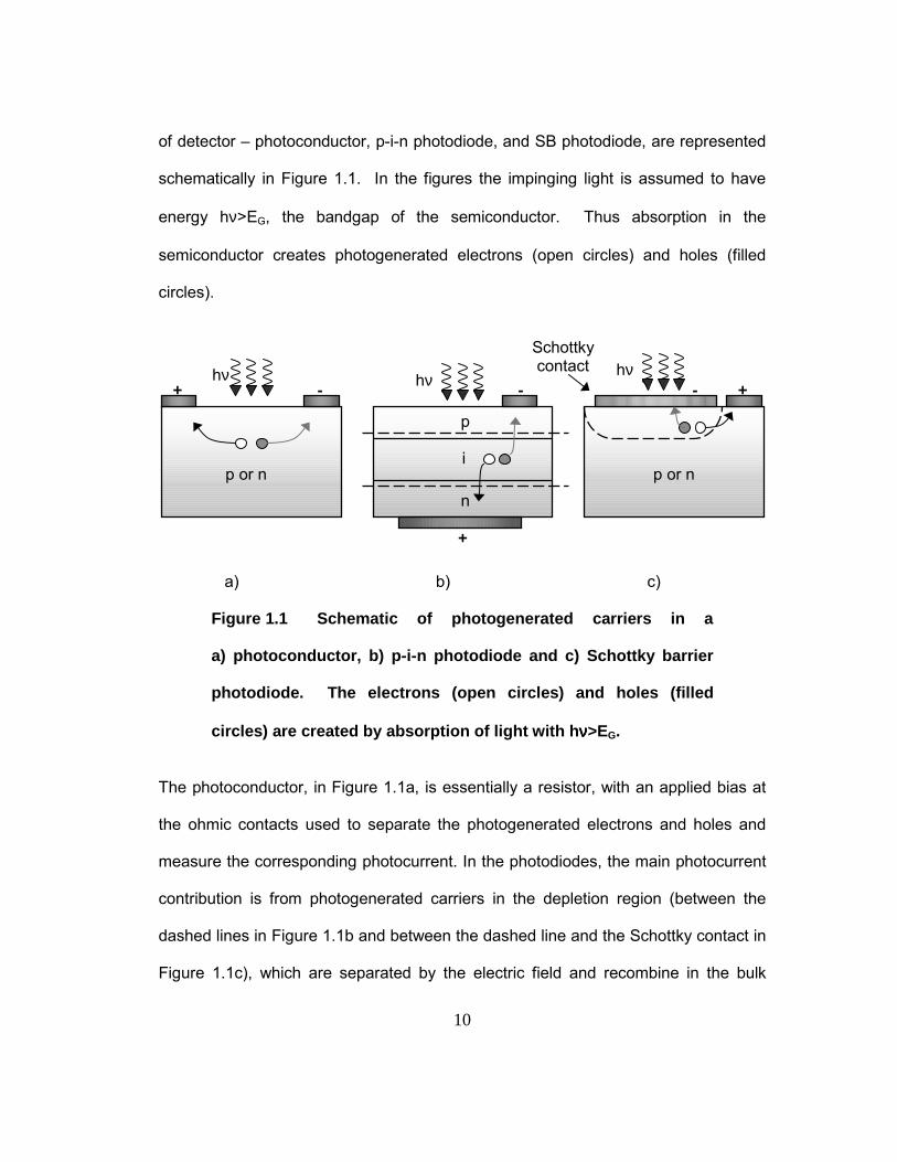
of detector � photoconductor, p-i-n photodiode, and SB photodiode, are represented
schematically in Figure 1.1. In the figures the impinging light is assumed to have
energy hν>EG, the bandgap of the semiconductor. Thus absorption in the
semiconductor creates photogenerated electrons (open circles) and holes (filled
circles).
a) b) c)
Figure 1.1 Schematic of photogenerated carriers in a
a) photoconductor, b) p-i-n photodiode and c) Schottky barrier
photodiode. The electrons (open circles) and holes (filled
circles) are created by absorption of light with hνννν>EG.
The photoconductor, in Figure 1.1a, is essentially a resistor, with an applied bias at
the ohmic contacts used to separate the photogenerated electrons and holes and
measure the corresponding photocurrent. In the photodiodes, the main photocurrent
contribution is from photogenerated carriers in the depletion region (between the
dashed lines in Figure 1.1b and between the dashed line and the Schottky contact in
Figure 1.1c), which are separated by the electric field and recombine in the bulk
hν
p
i
n
-
+
hν + -
p or n
hν - +
p or n
Schottky contact
11
regions or at the contacts. In all types of semiconductor photodetector the
mechanism of absorption of above-bandgap energy light to create photocurrent
means that the bandgap energy of the semiconductor determines the region of
operation (visible, infrared, ultraviolet) of the detector. As will be discussed in
Section 1.3.2, the bandgap range of AlxGa1-xN is ideally suited for ultraviolet
detectors.
Photoconductors have two major advantages - internal gain, and fabrication
simplicity - over photovoltaic devices. However they require biasing, exhibit high
dark, or leakage, currents, and furthermore are very slow when fabricated using
GaN-based material. Schottky barrier diodes are potentially the fastest detectors,
but suffer from worse leakage than p-i-n diodes due to the small barrier height, and
also from lower efficiency due to the narrow depletion region, combined with the
short diffusion lengths in GaN for carriers generated outside the depletion region.
Thus p-i-n diodes (with the i region inserted to extend the depletion region and thus
the high-field absorbing region of the detector) are the detectors of choice in this
work.
There are a number of figures of merit used to indicate photodetector performance.
The most fundamental of these is the responsivity, which measures detector output
for a given input, and is defined as:
=ℜ signal outputillumination input
. (1.1)
12
Signal output is measured either as a voltage or a current, and input as the power of
the target light-source, so that the conventional units of responsivity are V/W or A/W,
respectively. In this work current responsivity is used, so that:
λ
ην
= =ℜ photoi qP h
, (1.2)
in which iphoto is the photocurrent, Pλ the illumination power at wavelength λ
(frequency ν), and η the external quantum efficiency of the device. The energy of
the illumination increases with wavelength, and so therefore does the responsivity of
the detector. Due to the detection mechanism by photon absorption, photons of
energy less than the bandgap EG will not be absorbed. Thus there is a cutoff
wavelength, λc, beyond which the responsivity will be zero. There is further variation
in responsivity due to the convention of using input power in the calculation. The
number of photons per incident watt increases with wavelength so that R also
increases with wavelength until λc is reached.
Most other detector parameters are defined in terms of noise. Noise is electrical
output other than the desired detector signal, and can be either external (electrical
interference, amplifier noise) or fundamental to the detection process, such as the
non-constant arrival of photons, non-photonic generation and recombination of
carriers (such as thermal generation and recombination at traps), and random carrier
motion in the detector.
A commonly used figure of merit for photodiode noise is the zero-bias dynamic
resistance, Ro, of the device (measured in the absence of illumination), usually given
13
as RoA, where A is the area of the detector. In this work the currents near zero bias
were too low to be measured and so Ro could not used for evaluation of noise.
Instead the dark current measured in the absence of illumination is quoted; referred
to as the leakage current, JL, which is a measure of the noise at reverse bias (in
order for sufficient sensitivity of the device the leakage current must be much lower
in magnitude than the photocurrent). Most other reports of GaN and AlGaN UV
detectors in the literature also use this parameter. In the case of a wide-bandgap
semiconductor such as GaN and AlGaN the leakage current is expected to be limited
by surface leakage and/or space-charge region effects44.
Realistic assessment of the detector sensitivity requires consideration of both the
responsivity and the noise of the detector. The Noise Equivalent Power (NEP) is the
ratio of the two:
=ℜNINEP , (1.4)
in which IN is the root-mean-square (rms) noise current. However, this figure is still
dependent on the area of the diode.
Another figure of merit discussed in this work and in the literature is the response
time of the diode. The response time is usually limited by either the RC time
constant of the detector + circuit or the charge carrier lifetimes. The response time τ
will limit the bandwidth of the circuit:
πτ∆ = 1
2f (1.5)
14
In this study the speed of interest was the fall time of the detector response � the
decay rate of the signal output after illumination ceases, rather than the rise time of
the signal output after illumination initiates. For GaN-based detectors this has been
the more difficult parameter to control, as will be seen below.
The ultimate measure of detector performance is the Specific Detectivity, which is
independent of the detector area, A, and combines the responsivity, noise
performance and bandwidth of the detector:
∆=* A fD
NEP (1.6)
The larger D* is, the better the detector. When the detector is limited by thermal
noise the detectivity becomes45:
ηυ
=*
4oR AqD
h kT (1.7)
Thus a high Ro is desirable for high detectivity. Because Ro could not be measured,
detectivity figures could not be calculated for the detectors presented in this thesis.
1.3.2 What is solar-blind operation?
Of the various UV detector applications, many require detection of the target UV
signal in the presence of the immense background radiation signal of the sun. Within
a certain wavelength range the UV radiation from the sun is absorbed by the ozone
in the earth�s atmosphere and does not reach the earth�s surface. Figure 1.246
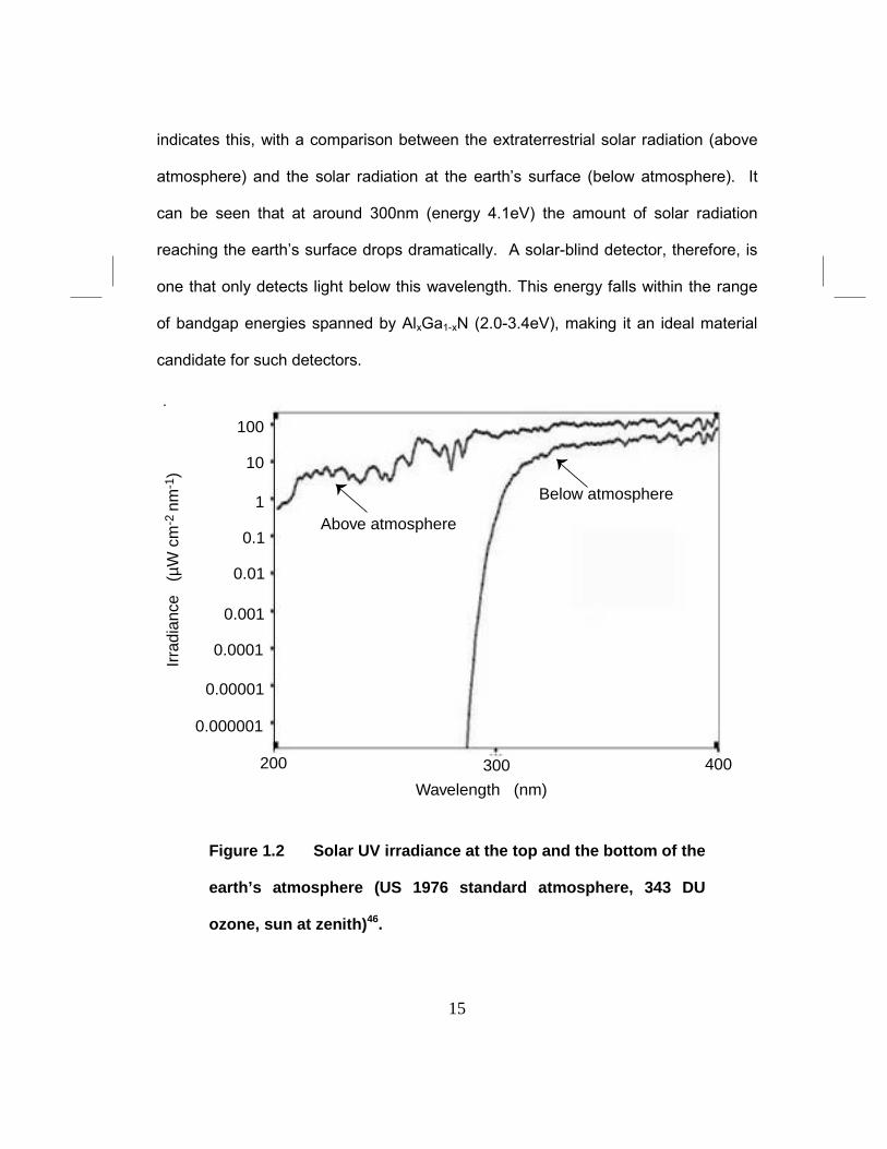
15
indicates this, with a comparison between the extraterrestrial solar radiation (above
atmosphere) and the solar radiation at the earth�s surface (below atmosphere). It
can be seen that at around 300nm (energy 4.1eV) the amount of solar radiation
reaching the earth�s surface drops dramatically. A solar-blind detector, therefore, is
one that only detects light below this wavelength. This energy falls within the range
of bandgap energies spanned by AlxGa1-xN (2.0-3.4eV), making it an ideal material
candidate for such detectors.
Above atmosphere
Below atmosphere
100
10
1
0.1
0.001
0.0001
0.00001
0.000001
0.01
200 300 400
Wavelength (nm)
Irra
dian
ce
(µW
cm
-2 n
m-1
)
Figure 1.2 Solar UV irradiance at the top and the bottom of the
earth’s atmosphere (US 1976 standard atmosphere, 343 DU
ozone, sun at zenith)46.
16
Review papers have had some variation on what the exact upper limit for solar-blind
character is � a paper summarizing UV detector requirements for AlGaN technology
in 199747 gave 300nm as the upper limit, while a recent study by Schreiber et al of
the US Airforce48 states 280nm to be the upper limit. Using the earlier information,
the solar-blind UV detectors in this study were designed to have a cutoff wavelength
below 300nm; which necessitates an AlGaN composition of greater than 30%. With
the revised definition of solar-blind limits a slight increase in composition will be
necessary for future work.
1.3.3. Visible-blind GaN-based detectors
The first GaN UV detector of any merit was a GaN photoconductor published by
Khan et al. in 199249. The devices had extremely high gains (peak responsivity of
1000A/W at 5V bias) but also high response times (1ms), due to a very long minority
carrier lifetime. In 1993 the same group published their first GaN SB photodiode50.
The first GaN p-n photodiode papers were published in 1995, by two separate
groups51,52. These first photovoltaic detectors also had slow response times (on the
order of µs for the SB and ms for the p-n). The problems of slow response time and
frequency- and power-dependence of responsivity experienced with the early
photoconductive devices have persisted in most reported photoconductive
devices30,31,49.
Improvements in material have allowed corresponding advancement of device
properties, particularly for the photovoltaic devices. SB devices have been recently
reported with peak responsivity of 0.19A/W, leakage currents of 3nA/cm2 at �5V and

17
RC-limited response times of 15ns53, while SB diodes deposited on LEO GaN were
reported with 1ns response time54. Visible-blind p-i-n photodiodes have been
reported with responsivities of 0.1-0.2 A/W, leakage currents of 2-12 nA/cm2 at �5V,
and response times of 12-17ns55,56,57,58. Some of the groups utilized an AlxGa1-xN
layer for the n-layer to give a narrow-band response when backside illuminated. The
use of a p-Al0.1Ga0.9N instead of p-GaN also was shown to improve responsivity and
speed58,59. Visible-blind GaN photodiodes have now reached such an acceptable
stage of technology that the first visible blind UV camera using a 32x32 array of
visible-blind p-GaN/i-GaN/n-Al0.2Ga0.8N detectors has been reported60.
1.3.4. Solar-blind AlGaN-based detectors
The first solar-blind detectors, reported in 1996 (by two separate groups), were
simple AlGaN photoconductors, which suffered from the same long minority carrier
lifetime-induced problems as GaN photoconductors, compounded by a high
resistance of the films30,31. In 1998 Osinsky et al. reported the first solar-blind SB
detector, with a peak responsivity of 0.07A/W at 290nm, but high leakage currents of
10µA/cm2 and slow response time of 1µs61. The following year, in collaboration with
Cree Lighting (then Nitres, Inc.) we reported the first solar-blind p-i-n photodiode,
with peak responsivities of 0.05A/W at 285nm and low leakage currents of 10nA/cm2
at �5V and response times of 4.5-6.5ns, when deposited on LEO GaN templates62.
These devices will be discussed in Chapter 3. Recently the focus in the GaN
research community has shifted from visible-blind to solar-blind detectors, with many
groups now improving material quality enough for realization of high quality AlGaN-
18
based detectors. Several groups have achieved this by use of higher xAl-buffers
enabling both higher quality AlGaN detector layers (deposited on top), and filtering
for backside illumination. Using this technique Karrer at al. reported the first fast
AlGaN photoconductors, with no gain (responsivity of 0.1A/W at 300nm) and
response times of 40ns63, and Lambert et al. demonstrated p-i-n diodes with
responsivity of 0.08 A/W at 278nm and leakage currents of 5nA/cm2 at �5V,
comparable to our results using LEO GaN64. The lowest leakage currents of 0.4-
3.5nA/cm2 at -5 V were reported by Pernot et al., using a dislocation reduction
technique involving an AlN interlayer (discussed in Chapter 2 and 3)65. However their
responsivities were low, only 0.012A/W at 270nm, with slow response times of 17µs.
Walker et al. also reported very high xAl (0.7-0.9) AlGaN p-i-n detectors with a peak
responsivity of 0.05A/W at 232 nm66. However the leakage currents were extremely
high, 400µA/cm2 at �10V. In their report no detail was given as to how growth of
such thick high-xAl structures was obtained, but these high leakage currents are an
indication that the AlGaN was highly defective and possibly even cracked (the diodes
were deposited on GaN templates).
1.4 Synopsis of this thesis
1.4.1 Chapter 2
With the requirement of solar-blind character of AlGaN-based detectors, the
development of MOCVD growth of high-quality AlxGa1-xN with xAl of 0.3 or greater
was a critical component of this dissertation. Chapter 2 details the development of
19
MOCVD growth of AlxGa1-xN using sapphire substrates, with xAl ranging from 0.2 to
0.65. The principles for MOCVD growth at UCSB are outlined, and some initial
studies into bulk AlGaN growth are presented. This is followed by investigations into
effect of growth conditions and xAl on AlGaN morphology and 2DEG properties,
which utilized thin AlGaN layers deposited on GaN base layers. Finally impurity
incorporation as a function of xAl and growth conditions will be discussed.
1.4.2 Chapter 3
Further to the studies of the AlGaN growth, are more fundamental studies regarding
the ever-present threading dislocations in epitaxially grown GaN and AlGaN. In
Chapter 3 several different studies of the effect of threading dislocations on
photodiode characteristics are presented. The first study looks at the effect of
different threading dislocation densities and makeup (screw, mixed, edge) on GaN p-
i-n diode leakage current and spectral response. This includes presentation of a
technique utilizing silicon nitride/InGaN interlayers to reduce edge dislocation
density. Following that the leakage current in GaN p-i-n diodes with a reduced TDD
is examined as a function of electric field/intrinsic layer thickness and diode size, to
ascertain other causes of leakage current besides threading dislocations. Finally the
photodetector characteristics (leakage current, spectral response, and pulsed
response) of solar-blind p-GaN/i-AlGaN/n-GaN diodes are compared with and
without threading dislocation reduction.
20
1.4.3 Chapter 4
In Chapter 4 further studies of the p-GaN/i-AlGaN/n-GaN solar-blind detector
structure are presented, with a view to an improved device design. Moves are made
to a detector with thicker i-AlGaN, and n-AlGaN instead of n-GaN. Unsuccessful
investigations into dislocation reduction utilizing LEO techniques for bulk Al0.35Ga0.65N
are presented. This is followed by experiments into the growth of thick Al0.35Ga0.65N
on SiC substrate. This was undertaken with the belief that the benefits to detector
performance, as well as the possibility of avoiding costly and time-consuming LEO,
would outweigh the increase in substrate cost ensuing from the use of SiC. These
experiments include studies of the nucleation technique and of the Al0.35Ga0.65N
growth conditions and doping, as well as attempts to reduced the high edge
dislocation density by using SixNy interlayers. Finally the results for solar-blind
AlxGa1-xN detectors grown on SiC substrates are presented, including a comparison
of devices with and without a conducting buffer.
1.5 References
1. H. Amano, N. Sawaki, I. Akasaki, and Y. Toyoda, �Metalorganic vapor phase epitaxial
growth of a high quality GaN film using an AlN buffer layer.� Appl. Phys. Lett. 48, 353-355
(1986).
2. S.T. Sheppard, K. Doverspike, W.L. Pribble, S.T. Allen, and J.W. Palmour, �High
power GaN/AlGaN HEMTs on silicon carbide�, 56th Annual Device Research Conference,
June 1998.
21
3. R. Gaska, J.W. Yang, A. Osinsky, Q. Chen, M. Asif Khan, A.O. Orlov, G.L. Snider,
and M.S. Shur, �Electron transport in AlGaN-GaN heterostructures grown on 6H-SiC
substrates.� Appl. Phys. Lett. 72, 707-709 (1998).
4. T.S. Zheleva, H. Nam, M.D. Bremser, and R.F. Davis, �Dislocation density reduction
via lateral epitaxy in selectively grown GaN structures.� Appl. Phys. Lett. 71, 2472-2474
(1997).
5. D. Kapolnek, S. Keller, R. Ventury, R.D. Underwood, P. Kozodoy, S.P. Den Baars,
and U.K. Mishra, �Anisotropic epitaxial lateral growth in GaN selective area epitaxy.� Appl.
Phys. Lett. 71, 1204-1206 (1997).
6. S. Nakamura, M. Senoh, S.I. Nagahama, N. Iwasa, T. Yamada, T. Matsushita, H.
Kiyoku, Y. Sugimoto, T. Kozaki, H. Umemoto, M. Sano and K. Chocho, �InGaN/GaN/AlGaN-
based laser diodes with modulation-doped strained-layer superlattices grown on an
epitaxially laterally overgrown GaN substrate.� Appl. Phys. Lett. 72, 211-213 (1998).
7. P. Kozodoy, J.P. Ibbetson, H. Marchand, P.T. Fini, S.Keller, J.S. Speck, S.P. Den
Baars, and U.K.Mishra, �Electrical characterization of GaN p-n junctions with and without
threading dislocations.� Appl. Phys. Lett. 73, 975-977 (1998).
8. R. Vetury, H. Marchand, G. Parish, P. T. Fini, J.P. Ibbetson, S. Keller, J. S. Speck, S.
P. DenBaars and U. K. Mishra, �First demonstration of AlGaN/GaN heterostructure field effect
transistor on GaN grown by lateral epitaxial overgrowth (LEO).� Proc. 25th Intl. Symp.
Compound Semicond. Nara, Japan 177-183 (1998).
9. W. Kim, A.E. Botchkarev, A. Salvador, G. Popovici, H. Tang & H. Morkoç, �On the
incorporation of Mg and the role of oxygen, silicon and hydrogen in GaN prepared by reactive
molecular beam epitaxy.� J. Appl. Phys. 82, 219-226 (1997).
10. C.Y. Hwang, Y. Li, M.J. Schurman, W. E. Mayo, Y. Lu & R.A. Stall, �The role of
impurities in LP-MOCVD grown gallium nitride.� Mat. Res. Soc. Symp. Proc.; 395, 521-526
(1996).

22
11. A.Y. Polyakov, M. Shin, D.W. Greve, M. Skowronski & R. G. Wilson, �High resistivity
AlxGa1-xN layers grown by MOCVD.� MRS Internet J. Nitride Semicond. Res. 1 (1996).
12. C.G. Van de Walle, C. Stampfl, and J. Neugebauer, �Theory of doping and defects in
III-V nitrides.� J. Cryst. Growth 189/190, 505-510 (1998).
13. M. Topf, W. Kriegseis, W. Burkhardt, I. Dirnstorfer, D. Meister and B.K. Meyer,
�Residual donors in GaN epitaxial films � a correlation of HALL effect, SIMS and
photoluminescence data.� Mater. Sci. Forum 264-268, 1323-1326 (1998).
14. C. Stampfl and C.G. Van de Walle, �Doping of AlxGa1-xN.� Appl. Phys. Lett. 72, 459-
461 (1998).
15. W. Seifert, R. Franzheld, E. Butter, H. Sobotta & V. Riede, � On the origin of free
carriers in high-conducting n-GaN.� Cryst. Res. & Technol. 18, 383-390 (1983).
16. B.-C. Chung & M. Gershenzon, �The influence of oxygen on the electrical and optical
properties of GaN crystals grown by metalorganic vapor phase epitaxy.� J. Appl. Phys. 72, 651-659 (1992).
17. C. Wetzel, H. Amano, I. Akasaki, T. Suski, J.W. Ager, E.R. Weber, E.E. Haller & B. K.
Meyer,� Localized donors in GaN: spectroscopy using large pressures.� Mat. Res. Soc.
Symp. Proc. 482, 489-500 (1998).
18. M.D. McCluskey, N. M. Johnson, C.G. Van de Walle, D.P. Bour, M. Kneissl and W.
Walukiewicz, �Metastability of oxygen donors in AlGaN.� Phys. Rev. Lett. 80, 4008-4011
(1998).
19. P. Boguslawski and J. Bernholc, �Doping properties of C, Si and Ge impurities in
GaN and AlN.� Phys. Rev. B. 56, 9496-9505 (1997).
20. T. Ogino and M. Aoki, �Mechanism of yellow luminescence in GaN.� Jpn. J. Appl.
Phys. 19, 2395-2405 (1980).
23
21. R. Zhang and T.F. Kuech, �Carbon and hydrogen induced yellow luminescence in
gallium nitride grown by halide vapor phase epitaxy.� Mat. Res. Soc. Symp. Proc. 482, 709-
714 (1998).
22. C.-Y. Hwang, M.J. Schurman, W. E. Mayo, Y.-C. Lu, R.A. Stall and T. Salagajj,
�Effect of structural defects and chemical impurities on Hall mobilities in low pressure
MOCVD grown GaN.� J. Electron. Mater. 26, 243-251 (1997)
23. J.Z. Li, J.Y. Lin, H.X. Jiang, M. Asif Khan and Q. Chen, �Persistent photoconductivity
in a tow-dimensional electron gas system formed by an AlGaN/GaN heterostructure.� J. Appl.
Phys. 82, 1227-1230 (1997).
24. F. Binet, J.Y. Duboz, E. Rosencher, F. Scholz and V. Härle, �Mechanisms of
recombination in GaN photodetectors.� Appl. Phys. Lett. 69, 1202-1204 (1996).
25. H. Amano, M. Kito, K. Hiramatsu, and I. Alasaki, �P-type conduction in Mg-doped
GaN treated with low-energy electron beam irradiation (LEEBI).� Jpn. J. Appl. Phys., Part 2.
28, L2112-L2214 (1989).
26. J.I. Pankove, �GaN and Related Materials� edited by S. J. Pearton (Gordon and
Breach, New York, 1997) pp.1-9.
27. C.G. Van de Walle, �Defects, doping and interfaces in III-V nitrides.� SPIE. 3283, 52-
59 (1998).
28. S. Nakamura, N. Iwasa, M. Senoh, and T. Mukai, �Hole compensation mechanism of
p-type GaN films.� Jpn. J. Appl. Phys., Part 1 31, 1258-1266 (1992).
29. P. Kozodoy, �Magnesium-doped gallium nitride for electronic and optoelectronic
device applications.� PhD Thesis, Electrical and Computer Engineering, University of
California, Santa Barbara (1999).
30. D. Walker X. Zhang, P. Kung, A. Saxler, S. Javadpour, J. Xu,. And M. Razeghi,
�AlGaN ultraviolet photoconductors grown on sapphire.� Appl. Phys. Lett. 68, 2100-2101
(1996).
24
31. B.W. Lim, Q.C. Chen, J.Y. Yang, and M. Asif Khan, �High responsivity intrinsic
photoconductors based on AlxGa1-xN.� Appl. Phys. Lett. 68, 3761-3762 (1996).
32. Y.-F. Wu, B.P. Keller, P. Fini, S. Keller, T.J. Jenkins, L.T. Kehias, S.P. DenBaars,
and U.K. Mishra, �High Al-content AlGaN/GaN MODFET�s for ultrahigh performance.� IEEE
Electron Lett. 19, 50-53 (1998).
33. M. Asif Khan, J.N. Kuznia, J.N. Van Hove, N. Pan, and J. Carter, �Observations of a
two-dimensional electron gas in a low pressure metalorganic chemical vapor deposited GaN-
AlxGa1-xN heterojunctions.� Appl. Phys. Lett. 60, 3027-3029 (1992).
34. M.A. Khan, J.N. Kuznia, D.T. Olson, W.J. Schaff, J.W. Burm, and M.S. Shur,
�Microwave performance of a 0.2µm gate AlGaN/GaN heterostructure field effect transistor.�
Appl. Phys. Lett. 65, 1121-1123 (1994).
35. J.P. Ibbetson, P.T. Fini, K.D. Ness, S.P. DenBaars, U.K. Mishra, and J.S. Speck,
�Polarization effects, surface states, and the source of electrons in AlGaN/GaN
heterostructure field effect transistors.� Appl. Phys. Lett. 77, 250-252 (2000).
36. F. Bernardini, V. Fiorentini, and D. Vanderbilt, �Spontaneous polarization and
piezoelectric constants of III-V nitrides.� Phys. Rev. B 56, R10024-10027 (1997).
37. Y.-F. Wu, S. Keller, P. Kozodoy, B.P. Keller, P. Parikh, D. Kapolnek, S.P. DenBaars,
and U.K. Mishra, �Bias dependent microwave performance of AlGaN/GaN MODFET�s up to
100 V.� IEEE Electron Device Lett.18, 290-292 (1997).
38. Y.-F. Wu, B.P. Keller, S. Keller, N.X. Nguyen, M. Le, C. Nguyen, T.J. Jenkins, L.T.
Kehias, S.P. DenBaars, and U.K. Mishra, �Short channel AlGaN/GaN MODFET�s with 50GHz
ft and 1.7 W/mm output power at 10 GHz.� IEEE Electron Device lett. 18, 438-440 (1997).
39. B.J. Thibeault, B.P. Keller, Y.-F. Wu, P. Fini, U.K. Mishra, C. Nguyen, N.X. Nguyen,
and M. Le, �High performance and large area flip-chip bonded AlGaN/GaN MODFET�s.� 56th
Annual Device Research Conference, Charlottesville, VA June 1998.
25
40. Y.-F.Wu, B.J.Thibeault, J.J. Xu, R.A. York, S. Keller, B.P. Keller, and U.K. Mishra,
�GaN HEMTs grown on sapphire substrates for microwave power amplification.� 57th IEEE
Device Research Conference, Santa Barbara, CA June 1999.
41. G. Parish, S. Keller, P. T. Fini, R. Vetury, C.-H. Chen, S. P. DenBaars, U. K. Mishra
and Y.-F. Wu, �MOCVD growth and properties of thin AlxGa1-xN layers on GaN.� Proc. IEEE
COMMAD Perth, Australia, 478-481 (1998).
42. S, Keller, G. Parish, P. T. Fini, S. Heikman, C.-H. Chen, N. Zhang, S. P. DenBaars
and U. K. Mishra, �Metalorganic chemical vapor deposition of high mobility AlGaN/GaN
heterostructures.� J. Appl. Phys. 86(10), 5850-5857 (1999).
43. �Nitres develops AlGaN/GaN HEMTs with record power performance." Compound
Semiconductor 6 (1), (2000).
44. M. Razeghi and A. Rogalski, �Semiconductor ultraviolet detectors.� J. Appl. Phys. 79,
7433-7473 (1996).
45. J.D. Brown, Zhonghai Yu, J. Mathews, S. Harney, J. Boney, J.F. Schetzina, J.D.
Benson, K.W. Dang, C. Terrill, T. Nohava, W. Yang, and S. Krishnankutty, �Visible-blind UV
digital camera based on 32x32 array of GaN/AlGaN p-i-n photodiodes.� MRS Internet J.
Nitride Semicond. Res 4, 9 (1999).
46. Figure provided by B.D. Nener (private communication), The University of Western
Australia (2001).
47. M. Razeghi and A. Rogalski, �AlGaN ultraviolet detectors.� Proc. SPIE 2999, 275-286
(1997).
48. P. Schreiber, T. Dang, G. Smith, T. Pickenpaugh, P. Gerhed, D. Littleton, �Solar blind
UV region and UV detector development objectives.� Proc. SPIE 3629, 230-248 (1999).
49. M. Asif Khan, J.N. Kuznia, D.T. Olson, J.M. Van Hove, M. Blasingame, and L.F.
Reitz, �High-responsivity photoconductive ultraviolet sensors based on insulating single-
crystal GaN epilayers.� Appl.Phys. Lett. 60 (23), 2917-2919 (1992).
26
50. M. Asif Khan, J.N. Kuznia, D.T. Olson, M. Blasingame, and A.R Bhattarai, �Schottky
barrier photodetector based on Mg-doped p-type GaN films.� Appl. Phys. Lett. 63 (18), 2455-
2456 (1993).
51. Q. Chen, M. Asif Khan, C.J. Sun, and J.W. Yang, �Visible-blind ultraviolet
photodetectors based on GaN p-n junctions.� Electronics Letters 31 (20), 1781-1782 (1995).
52. X. Zhang, P. Kung, D. Walker, J. Piotrowski, A. Rogalski, A. Saxler, and M. Razeghi,
�Photovoltaic effects in GaN structures with p-n junctions.� Appl. Phys. Lett. 67, 2028-2030
(1995).
53. V. Adivarahan, G. Simin, J.W. Yang, A. Lunev, M. Asif Khan, N.Pala, M. Shur, and R.
Gaska, �SiO2-passivated lateral-geometry GaN transparent Schottky-barrier detectors.� Appl.
Phys. Lett. 77, 863-865 (2000).
54. E. Monroy, F. Calle, E. Muñoz, B. Beaumont, F. Omnès, and P. Gibart, �High
UV/visible contrast photodiodes based on epitaxial lateral overgrown GaN layers.� Electronics
Letters 35, 1488-1489 (1999).
55. A. Osinsky, S. Gangopadhyay, R. Gaska, B. Williams, M.A. Khan, D Kuksenkov, and
H. Temkin, �Low noise p-π-n GaN ultraviolet photodetectors.� Appl. Phys. Lett. 71, 2334-2336
(1997).
56. J.C. Carrano, T. Li, P.A. Grudowski, C.J. Eiting, D. Lambert, J.D. Schaub, R.D.
Dupuis, and J.C. Campbell, �Low dark current pin ultraviolet photodetectors fabricated on
GaN grown by metal organic chemical vapor deposition.� Electronics Letters 34, 692-694
(1998).
57. W. Yang, T. Nohova, S. Krishnankutty, R. Torreano, S.t McPherson, and H. Marsh,
�Back-illuminated GaN/AlGaN heterojunction photodiodes with high quantum efficiency and
low noise.� Appl. Phys. Lett. 73, 1086-1088 (1998).
58. G. Smith, M.J. Estes, T. Dang, A.A. Salvador, Z. Fan, G. Xu, A. Botchkarev, H.
Morkoc, and P. Wolf, �Megahertz bandwidth AlxGa1-xN/GaN-based pin detectors.� Proc. SPIE
3287, 198-205 (1998).
27
59. T. Li, A.L. Beck, C. Collins, R.D. Dupuis, J.C. Campbell, J.C. Carrano, M.J.
Schurman, and I.A. Ferguson, �Improved ultraviolet quantum efficiency using a
semitransparent recessed window AlGaN/GaN heterojunction p-i-n photodiode.� Appl. Phys.
Lett. 75, 2421-2423 (1999).
60. J.D. Brown, Zhonghai Yu, J. Mathews, S. Harney, J. Boney, J.F. Schetzina, J.D.
Benson, K.W. Dang, C. Terrill, T. Nohava, W. Yang, and S. Krishnankutty, �Visible-blind UV
digital camera based on 32x32 array of GaN/AlGaN p-i-n photodiodes.� MRS Internet J.
Nitride Semicond. Res. 4, 9 (1999).
61. A. Osinsky, S. Gangopadhyay, B.W. Lim, M.Z. Anwar, M.A. Khan, D.V. Kuksenkov,
and H. Temkin, �Schottky barrier photodetectors based on AlGaN.� Appl. Phys. Lett. 72, 742-
744 (1998).
62. G. Parish, S. Keller, P. Kozodoy, J. P. Ibbetson, H. Marchand, P. T. Fini, S.B.
Fleischer, S. P. DenBaars, U. K. Mishra and E.J. Tarsa, �High-performance (Al,Ga)N-based
solar-blind ultraviolet p-i-n detectors on laterally epitaxially overgrown GaN.� Appl. Phys. Lett.
75(2), 247-249 (1999).
63. U. Karrer, A. Dobner, O. Ambacher, and M. Stutzmann, �AlGaN-based ultraviolet light
detectors with integrated optical filters.� J. Vac. Sci. Technol.B 18, 757-760 (2000).
64. D.H. Lambert, M.M. Wong, U. Chowdhury, C. Collins, T. Li, K. Kwon, B.S. Shelton,
T.G. Zhu, J.C. Campbell, and R.D. Dupuis, �Back illuminated AlGaN solar-blind
photodetectors.� Appl. Phys. Lett. 77, 1090-1092 (2000)
65. C. Pernot, A. Hirano, M. Iwaya, T. Detchprohm, H. Amano, and I. Akasaki, �Solar-
blind UV photodetectors based on GaN/AlGaN p-i-n photodiodes.� Jpn. J. Appl. Phys. 39, 387-389 (2000).
66. D. Walker, V. Kumar, K. Mi, P. Sandvik, P. Kung, and M. Razeghi, �Solar-blind
AlGaN photodiodes with very low cutoff wavelength.� Appl. Phys. Lett. 76, 403-405 (2000).
28
Chapter 2. AlGaN growth using sapphire substrate
2.1 Introduction
As described in the introductory chapter, the focus of this work is on the development
of AlxGa1-xN for solar-blind photodetectors, and thus of AlxGa1-xN with greater than
30% aluminum content. Literature detailing growth investigations of such high-
composition AlGaN has been minimal, although in recent years it has been receiving
more attention. In general, however, when reviewing both the literature and the
results presented in this chapter, it becomes apparent that alloying GaN with
significant quantities of Al presents more challenges to growth than with GaN alone.
2.1.1 Epitaxially grown bulk AlGaN
At the onset of this study, it was evident from the literature that bulk AlGaN of a high
structural and electrical quality is very difficult to grow1,2,3,4,5. It is hard to achieve
atomically smooth, step-flow growth of compositionally uniform, defect-free, and,
depending on the substrate, crack-free AlGaN of high composition. Recent results of
Al0.5Ga0.5N deposited on bulk AlN substrates6 are at a very early stage of
development, although use of this substrate is expected to eventually show
improvement. Most bulk AlGaN reported has, as with GaN, been deposited on
sapphire substrates. Again, similarly to GaN, the use of a low temperature nucleation
layer was shown to help.7 Many recent reports reveal little progress in overcoming
the difficulties in AlGaN growth8,9,10. One notable exception has been the work of
Iwaya et al.11. This group has achieved pronounced improvements in quality of thick
29
(>1µm) AlxGa1-xN layers deposited on a low-temperature AlN interlayer on GaN
templates on sapphire (with an AlN nucleation layer), with no degradation in
properties as xAl is raised. Also, recently reported UV detectors fabricated from bulk
AlGaN grown on sapphire substrate with a thick higher-xAl AlGaN buffer have
indicated AlGaN of relatively high quality12,13.
Compounding the difficulties in obtaining device-quality AlGaN is the difficulty in
doping. Many of the studies referenced above reported a monotonic increase in
resistivity (with a decrease in both carrier concentration and mobility) of undoped
AlGaN with increasing Al content (at low compositions, undoped AlGaN is usually n-
type). Even when doped intentionally n-type with silicon or germanium, electrically
conducting material has not been obtained for xAl greater than 0.51,3. Although there
has been much theoretical and experimental research into the insulating nature of
AlGaN and AlGaN:Si, controversy about its cause still exists. There is general
agreement that oxygen, a shallow donor in GaN, and ever-present in MOCVD-grown
AlGaN, becomes a DX center in AlxGa1-xN above xAl=0.314. More questionable is
whether in addition to an increase in ionization energy as the bandgap widens, Si
becomes a DX center, or whether some other defect such as Al vacancies cause
compensation15,16. Furthermore, p-type doping has not been reported for AlxGa1-xN
at the compositions of interest in this study. However even for lower compositions of
xAl = 0.1-0.2, research again shows that p drops significantly as xAl is increased17,3.
As in the case of silicon doping, this is due at least in part to the increase in
activation energy of Mg as xAl, and hence EG, increases15.
30
2.1.2 AlGaN/GaN heterostructures
The growth of AlGaN/GaN heterostructures is also difficult, exacerbated by the lattice
and thermal mismatch between the AlGaN and the underlying GaN (aGaN = 3.189Å,
aAlN = 3.112Å at 300K; αGaN = 5x10⁻⁶K-1, αAlN = 5.3x10⁻⁶K-1 at 600K18). To avoid
cracking, the AlGaN layers must be thin, so that an assessment of bulk AlGaN
properties cannot be obtained with such structures. Nevertheless, Hall
measurements of the 2DEG formed at the AlGaN/GaN interface allow some
assessments with regard to AlGaN quality. This is especially advantageous when
considering that for bulk AlGaN the difficulty in obtaining low-resistance material
precludes effective electrical measurements. Hall studies of the 2DEG, including
temperature-dependent measurements, can indicate the effects of alloy clustering,
interface roughness, dislocations and point defects. Furthermore, epitaxial growth of
thin layers on a standard GaN template allows the surface morphology to be
assessed with respect to growth conditions without the need to develop unique
nucleation schemes for each AlGaN composition. Very little had been published
regarding AlGaN/GaN heterostructures when we began our studies. Some of the
results which we previously published, and are presented here, have been confirmed
by others such as Eiting et al.19
2.1.3 Synopsis of the chapter
This chapter will detail the development of MOCVD growth of AlxGa1-xN using
sapphire substrates, with xAl ranging from 0.2 to 0.65. In Section 2.1 the principles
31
for MOCVD growth at UCSB are outlined, and some initial studies into bulk AlGaN
growth are presented. This is followed in Section 2.2 by the investigations into the
effect of growth conditions and xAl on AlGaN morphology and 2DEG properties,
which utilized thin AlGaN layers deposited on GaN base layers. Finally in Section 2.4
impurity incorporation as a function of xAl and growth conditions will be discussed.
2.2 MOCVD Growth at UCSB
The material for the growth studies presented in this chapter was grown by MOCVD
in a two-flow horizontal quartz reactor, using the precursors trimethylgallium (TMGa),
trimethylaluminum (TMAl) and ammonia. Disilane (DiSi) was used for n-type doping
with Si. For the AlGaN/GaN heterostructures the growth of the GaN base layers was
initiated on the sapphire substrate with an approximately 20 nm thick GaN layer
grown at 525 °C while the main GaN layer was grown at temperatures between 1040
and 1125 °C20. A wide parameter space was explored for the growth of the AlGaN
layers: The TMGa flow and the TMAl flow were varied between 0.6 � 77 µmol/min
and the ammonia flow between 0.03 � 0.32 mol/min. Variations in growth rate were
achieved by changing the group III flows. The growth temperature ranged from 800
to 1125 °C. The growth temperature was measured by means of a thermocouple
inserted into the graphite susceptor, protected by a quartz sheath. The total gas flow
was kept constant at 11 l/min. The reactor pressure for GaN and AlGaN growth was
760 and 76 torr, respectively, except for the impurity incorporation experiments,
when 300 torr was also used.
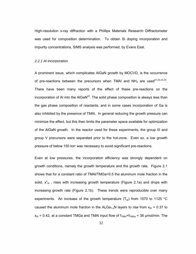
32
High-resolution x-ray diffraction with a Phillips Materials Research Diffractometer
was used for composition determination. To obtain Si doping incorporation and
impurity concentrations, SIMS analysis was performed, by Evans East.
2.2.1 Al incorporation
A prominent issue, which complicates AlGaN growth by MOCVD, is the occurrence
of pre-reactions between the precursors when TMAl and NH3 are used21,22,23,24.
There have been many reports of the effect of these pre-reactions on the
incorporation of Al into the AlGaN22. The solid phase composition is always less than
the gas phase composition of reactants, and in some cases incorporation of Ga is
also inhibited by the presence of TMAl. In general reducing the growth pressure can
minimize the effect, but this then limits the parameter space available for optimization
of the AlGaN growth. In the reactor used for these experiments, the group III and
group V precursors were separated prior to the hot-zone. Even so, a low growth
pressure of below 150 torr was necessary to avoid significant pre-reactions.
Even at low pressures, the incorporation efficiency was strongly dependent on
growth conditions, namely the growth temperature and the growth rate. Figure 2.1
shows that for a constant ratio of TMAl/TMGa=0.5 the aluminum mole fraction in the
solid, xsAl , rises with increasing growth temperature (Figure 2.1a) and drops with
increasing growth rate (Figure 2.1b). These trends were reproducible over many
experiments. An increase of the growth temperature (Tgr) from 1070 to 1125 °C
caused the aluminum mole fraction in the AlxGa1-xN layers to rise from xAl = 0.37 to
xAl = 0.42, at a constant TMGa and TMAl input flow of fTMAl+fTMGa = 38 µmol/min. The
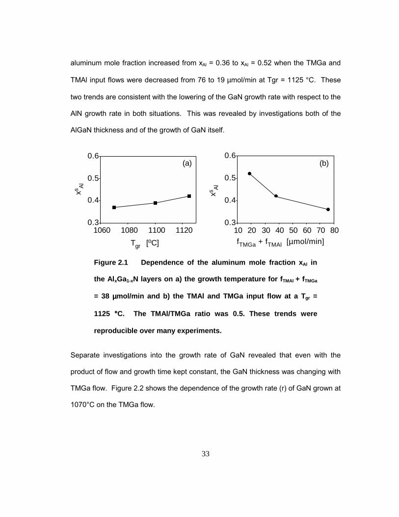
33
aluminum mole fraction increased from xAl = 0.36 to xAl = 0.52 when the TMGa and
TMAl input flows were decreased from 76 to 19 µmol/min at Tgr = 1125 °C. These
two trends are consistent with the lowering of the GaN growth rate with respect to the
AlN growth rate in both situations. This was revealed by investigations both of the
AlGaN thickness and of the growth of GaN itself.
fTMGa + fTMAl [µmol/min] 10 20 30 40 50 60 70 80
xs Al
0.3
0.4
0.5
0.6(b)
Tgr [oC]
1060 1080 1100 11200.3
0.4
0.5
0.6(a)
xs Al
Figure 2.1 Dependence of the aluminum mole fraction xAl in
the AlxGa1-xN layers on a) the growth temperature for fTMAl + fTMGa
= 38 µµµµmol/min and b) the TMAl and TMGa input flow at a Tgr =
1125 °°°°C. The TMAl/TMGa ratio was 0.5. These trends were
reproducible over many experiments.
Separate investigations into the growth rate of GaN revealed that even with the
product of flow and growth time kept constant, the GaN thickness was changing with
TMGa flow. Figure 2.2 shows the dependence of the growth rate (r) of GaN grown at
1070°C on the TMGa flow.
34
0.00
0.20
0.40
0.60
0.80
1.00
1.20
0 5 1 0 1 5 2 0 2 5 3 0 3 5 4 0
Gro
wth
rat
e, r
(n
m/s
)
TMGa flow, fTMGa (µmol/min)
Figure 2.2 Growth rate as a function of TMGa flow for GaN
grown at 1070°C, 760 torr and NH3 flow of 0.27 mol/min.
Experimental results are shown in black. The grey dotted line
assumes ideal (linear) behavior for the highest input flow.
The grey dotted line assumes ideal (linear) behavior for the highest input flow. It is
evident that there is a non-linear dependence; with the growth rate slowing at lower
flows. Even at a relatively high growth rate of 0.48 nm/s (1.74 µm/hr) this non-
linearity already exists. A linear dependence is expected only when the input partial
pressure of Ga-species, oGap , is much higher than the equilibrium partial pressure of
the gallium, eqGap , so that eq
Gap can be neglected.

35
If eqGap can be neglected then
( )eqGa
oGa ppr −∝ (2.1)
may be simplified to
oGapr ∝ (2.2)
where oGap is proportional to the TMGa input flow.25�26 At low input flows and high
temperatures (and therefore high eqGap ) this simplification is not valid and this results
in the non-linear dependence seen in Figure 2.2. In addition to this, higher growth
temperatures will lower the sticking probability of Ga-species on the epitaxial surface.
On the other hand, eqAlp is always much smaller than o
Alp under the experimental
conditions in this study and can be neglected. Hence, with increasing Tgr and
decreasing oGap , the composition of the AlGaN is given by
( )( ) ( )eq
GaoGaGa
oAlAl
oAlAls
Al ppkpkpkx
−+= . (2.3)
In the above equation kAl and kGa are the transport coefficients, which represent the
incorporation efficiency for the entire growth process (including pre-reactions, gas-
phase transport, surface kinetics and so on).
36
2.2.2 Bulk AlGaN growth on sapphire
Initial, limited studies into the bulk growth of AlGaN on sapphire substrates were
carried out at UCSB. Different nucleation and growth conditions were attempted,
without success in simultaneously achieving smooth, specular and crack-free layers.
The first attempts utilized the same nucleation scheme as was used for GaN
templates. After deposition of a 200Å low-temperature GaN nucleation layer, thin
high temperature layers of 500-2000Å GaN were grown, followed by 1-1.5µm bulk
Al0.3Ga0.7N layers. The AlGaN layers were grown at 1080°C, a slightly higher
temperature than for GaN layers, with growth conditions otherwise comparable to
GaN template growth. These films were not specular, and exhibited (0002) rocking-
curve full-width half-maximum (FWHM) values of 1200-1600 arc-seconds. Similar
AlGaN films were deposited on thin AlN layers obtained by high-temperature
exposure of the sapphire (Al2O3) to NH3. Again the films were not specular, with
large hexagonal surface features visible by optical microscopy, although the FWHM
values were reduced to 600-700 arc-seconds. Finally, the bulk layers were again
initiated with deposition of a 200Å low-temperature GaN nucleation layer, this time
followed by thin higher-temperature layers of 300-700Å GaN grown at 76 torr (the
lower pressure induces faster coalescence of the nucleation islands due to increased
lateral overgrowth), and 1µm bulk Al0.3Ga0.7N layers. In this case the AlGaN layers
were growth under low-ammonia conditions, as this had been found to improve the
surface morphology of thin AlGaN layers on GaN (see next section for discussion of
these studies). The films obtained this way were in fact specular, but optical
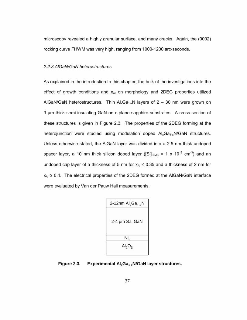
37
microscopy revealed a highly granular surface, and many cracks. Again, the (0002)
rocking curve FHWM was very high, ranging from 1000-1200 arc-seconds.
2.2.3 AlGaN/GaN heterostructures
As explained in the introduction to this chapter, the bulk of the investigations into the
effect of growth conditions and xAl on morphology and 2DEG properties utilized
AlGaN/GaN heterostructures. Thin AlxGa1-xN layers of 2 � 30 nm were grown on
3 µm thick semi-insulating GaN on c-plane sapphire substrates. A cross-section of
these structures is given in Figure 2.3. The properties of the 2DEG forming at the
heterojunction were studied using modulation doped AlxGa1-xN/GaN structures.
Unless otherwise stated, the AlGaN layer was divided into a 2.5 nm thick undoped
spacer layer, a 10 nm thick silicon doped layer ([Si]SIMS = 1 x 1019 cm-3) and an
undoped cap layer of a thickness of 5 nm for xAl ≤ 0.35 and a thickness of 2 nm for
xAl ≥ 0.4. The electrical properties of the 2DEG formed at the AlGaN/GaN interface
were evaluated by Van der Pauw Hall measurements.
2-12nm AlxGa1-xN
2-4 µm S.I. GaN
Al2O3
NL
Figure 2.3. Experimental AlxGa1-xN/GaN layer structures.
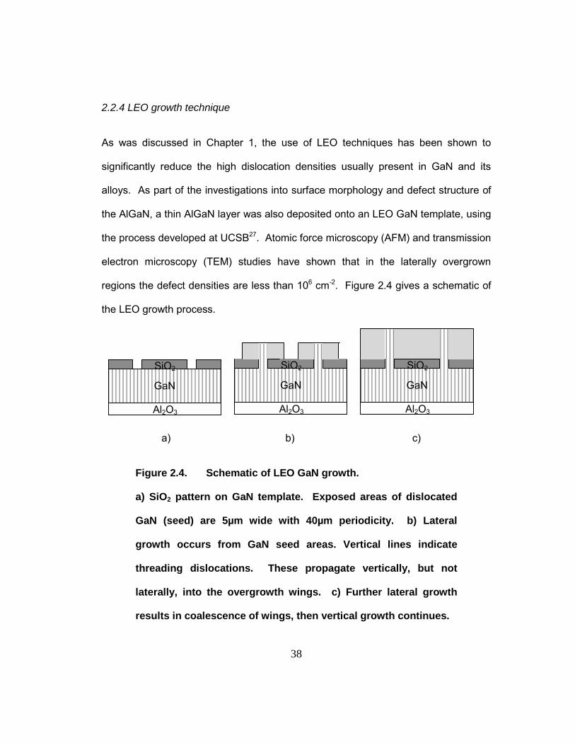
38
2.2.4 LEO growth technique
As was discussed in Chapter 1, the use of LEO techniques has been shown to
significantly reduce the high dislocation densities usually present in GaN and its
alloys. As part of the investigations into surface morphology and defect structure of
the AlGaN, a thin AlGaN layer was also deposited onto an LEO GaN template, using
the process developed at UCSB27. Atomic force microscopy (AFM) and transmission
electron microscopy (TEM) studies have shown that in the laterally overgrown
regions the defect densities are less than 106 cm-2. Figure 2.4 gives a schematic of
the LEO growth process.
a) b) c)
Figure 2.4. Schematic of LEO GaN growth.
a) SiO2 pattern on GaN template. Exposed areas of dislocated
GaN (seed) are 5µm wide with 40µm periodicity. b) Lateral
growth occurs from GaN seed areas. Vertical lines indicate
threading dislocations. These propagate vertically, but not
laterally, into the overgrowth wings. c) Further lateral growth
results in coalescence of wings, then vertical growth continues.
SiO2
GaN
Al2O3
SiO2
GaN
Al2O3
SiO2
GaN
Al2O3
39
For the LEO GaN template, a 2µm thick GaN wafer was patterned with SiO2 stripes.
These stripes were 35 µm wide, with a periodicity of 40 µm. This left 5µm stripes of
the underlying GaN (seed region) exposed. Subsequent regrowth on this wafer
resulted in selective epitaxial growth of GaN wings laterally across the SiO2 mask.
2.3 Surface morphology of AlGaN/GaN heterostructures
The surface morphology of the layers was studied by atomic force microscopy (AFM)
using a Digital Instruments Nanoscope III, operated in tapping mode. The root-
mean-square (RMS) roughness of the surfaces was calculated using the AFM
software.
2.3.1 Effect of xAl
AFM imaging of the thin AlGaN layers revealed a very strong dependence of the
surface morphology on the composition. Figure 2.5 presents the AFM images of the
surfaces of 18 nm thick AlxGa1-xN films, with xAl values of (a) 0.2, (b) 0.4 and (c) 0.6,
along with (d) the surface of a typical GaN base film. The surface of the Al0.2Ga0.8N
film (Figure 2.5a) resembles the surface of the GaN base film (Figure 2.5d). The
surface is characterized by a step-like structure. Each step corresponds to an
(Al,Ga)-N bi-layer. The steps merge at threading dislocations with a screw
component, which are seen as dark spots in the image. The smaller dark spots,
which are independent of the step structure, originate from edge dislocations28.
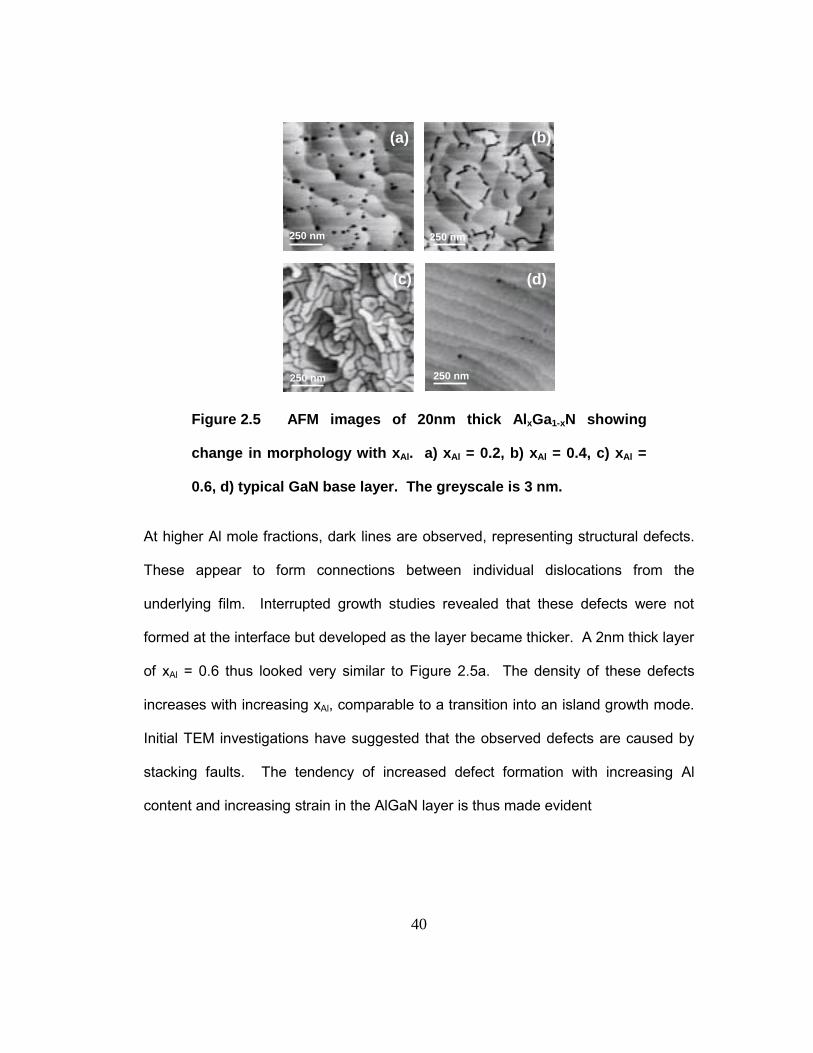
40
250 nm
(a)
250 nm
(a) (b)
(c)
250 nm
250 nm
(d)
250 nm
Figure 2.5 AFM images of 20nm thick AlxGa1-xN showing
change in morphology with xAl. a) xAl = 0.2, b) xAl = 0.4, c) xAl =
0.6, d) typical GaN base layer. The greyscale is 3 nm.
At higher Al mole fractions, dark lines are observed, representing structural defects.
These appear to form connections between individual dislocations from the
underlying film. Interrupted growth studies revealed that these defects were not
formed at the interface but developed as the layer became thicker. A 2nm thick layer
of xAl = 0.6 thus looked very similar to Figure 2.5a. The density of these defects
increases with increasing xAl, comparable to a transition into an island growth mode.
Initial TEM investigations have suggested that the observed defects are caused by
stacking faults. The tendency of increased defect formation with increasing Al
content and increasing strain in the AlGaN layer is thus made evident
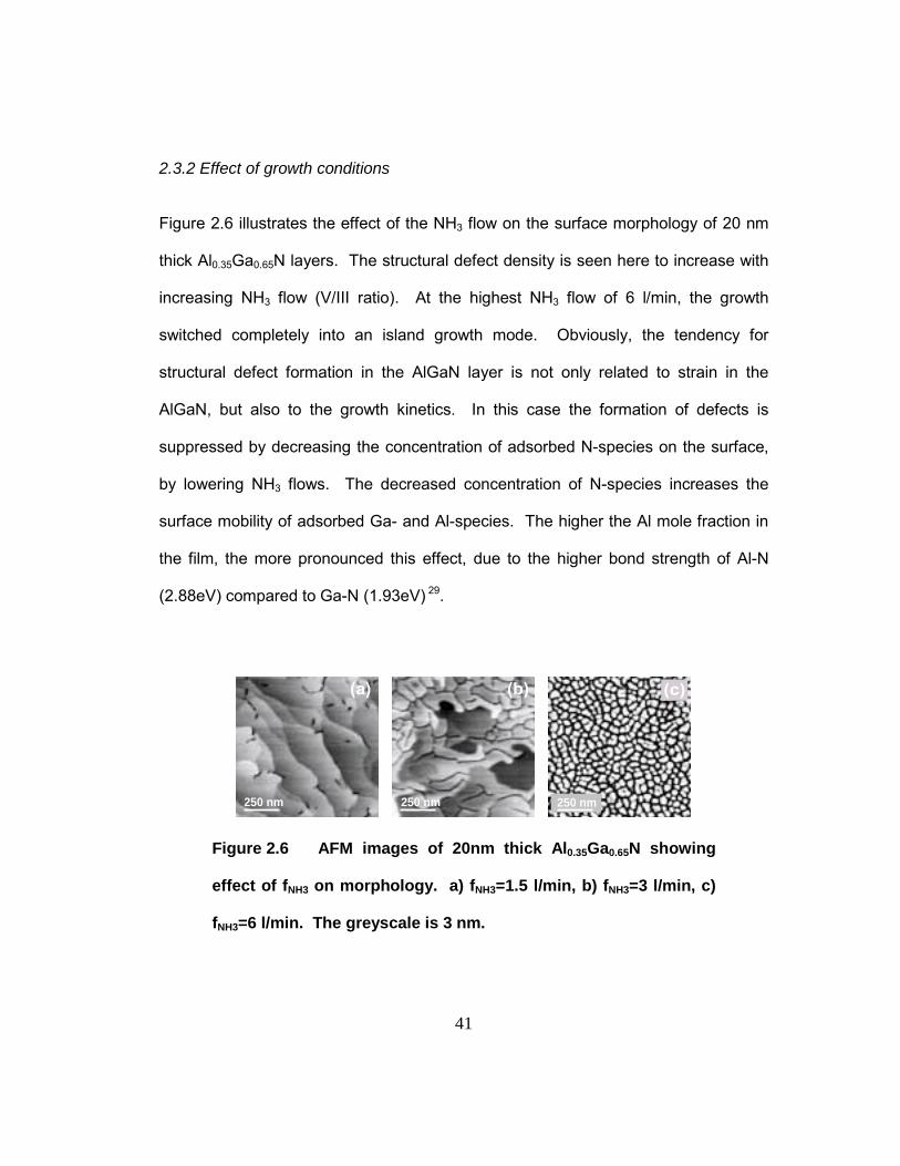
41
2.3.2 Effect of growth conditions
Figure 2.6 illustrates the effect of the NH3 flow on the surface morphology of 20 nm
thick Al0.35Ga0.65N layers. The structural defect density is seen here to increase with
increasing NH3 flow (V/III ratio). At the highest NH3 flow of 6 l/min, the growth
switched completely into an island growth mode. Obviously, the tendency for
structural defect formation in the AlGaN layer is not only related to strain in the
AlGaN, but also to the growth kinetics. In this case the formation of defects is
suppressed by decreasing the concentration of adsorbed N-species on the surface,
by lowering NH3 flows. The decreased concentration of N-species increases the
surface mobility of adsorbed Ga- and Al-species. The higher the Al mole fraction in
the film, the more pronounced this effect, due to the higher bond strength of Al-N
(2.88eV) compared to Ga-N (1.93eV) 29.
(a) (b) (c)
250 nm250 nm 250 nm
Figure 2.6 AFM images of 20nm thick Al0.35Ga0.65N showing
effect of fNH3 on morphology. a) fNH3=1.5 l/min, b) fNH3=3 l/min, c)
fNH3=6 l/min. The greyscale is 3 nm.
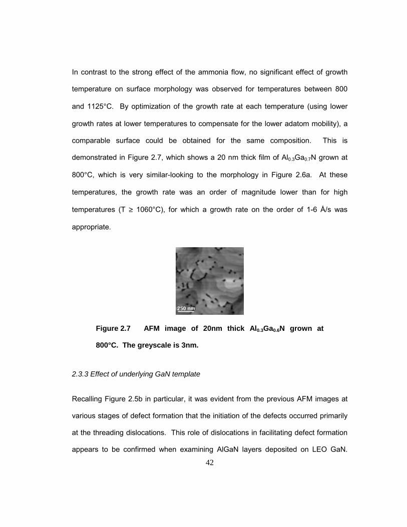
42
In contrast to the strong effect of the ammonia flow, no significant effect of growth
temperature on surface morphology was observed for temperatures between 800
and 1125°C. By optimization of the growth rate at each temperature (using lower
growth rates at lower temperatures to compensate for the lower adatom mobility), a
comparable surface could be obtained for the same composition. This is
demonstrated in Figure 2.7, which shows a 20 nm thick film of Al0.3Ga0.7N grown at
800°C, which is very similar-looking to the morphology in Figure 2.6a. At these
temperatures, the growth rate was an order of magnitude lower than for high
temperatures (T ≥ 1060°C), for which a growth rate on the order of 1-6 Å/s was
appropriate.
250 nm
Figure 2.7 AFM image of 20nm thick Al0.3Ga0.6N grown at
800°C. The greyscale is 3nm.
2.3.3 Effect of underlying GaN template
Recalling Figure 2.5b in particular, it was evident from the previous AFM images at
various stages of defect formation that the initiation of the defects occurred primarily
at the threading dislocations. This role of dislocations in facilitating defect formation
appears to be confirmed when examining AlGaN layers deposited on LEO GaN.

43
Figure 2.8 is an AFM image of a 20nm Al0.3Ga0.7N layer grown on an LEO GaN
template. A much higher number of structural defects are visible in the dislocated
seed region.
wing seed
2 µm
Figure 2.8. AFM image across seed and wing regions of
Al.3Ga.7N/GaN heterostructure, showing change in dislocation
structure and morphology on LEO GaN wings.
2.4. Electrical properties of AlGaN/GaN heterostructures
Standard Hall measurements using a Van der Pauw pattern were taken at 300K and
at 77K for the AlGaN/GaN heterostructures. This allowed assessment of the effect
of different AlGaN growth conditions and compositions on the sheet charge and
mobility of the 2DEG. To ensure optimal quality for device applications all of the
AlGaN films under discussion in this section were grown with a low NH3 flow of
1.5l/min. For some structures temperature-dependent Hall was also measured
between 77 and 300K.
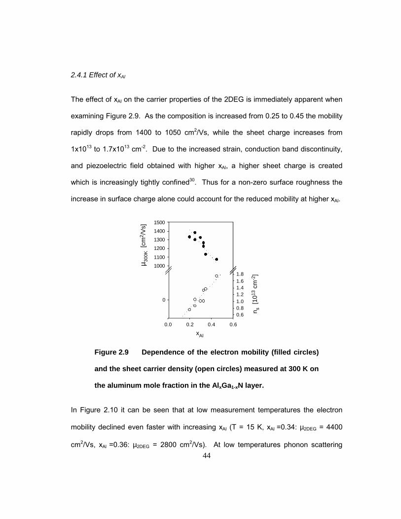
44
2.4.1 Effect of xAl
The effect of xAl on the carrier properties of the 2DEG is immediately apparent when
examining Figure 2.9. As the composition is increased from 0.25 to 0.45 the mobility
rapidly drops from 1400 to 1050 cm2/Vs, while the sheet charge increases from
1x10¹³ to 1.7x1013 cm-2. Due to the increased strain, conduction band discontinuity,
and piezoelectric field obtained with higher xAl, a higher sheet charge is created
which is increasingly tightly confined30. Thus for a non-zero surface roughness the
increase in surface charge alone could account for the reduced mobility at higher xAl.
xAl 0.0 0.2 0.4 0.6
n s [1
013 c
m-2
]
0.60.81.01.21.41.61.8
µ 300
K [
cm2 /
Vs]
0
1000
1100
1200
1300
1400
1500
Figure 2.9 Dependence of the electron mobility (filled circles)
and the sheet carrier density (open circles) measured at 300 K on
the aluminum mole fraction in the AlxGa1-xN layer.
In Figure 2.10 it can be seen that at low measurement temperatures the electron
mobility declined even faster with increasing xAl (T = 15 K, xAl =0.34: µ2DEG = 4400
cm2/Vs, xAl =0.36: µ2DEG = 2800 cm2/Vs). At low temperatures phonon scattering
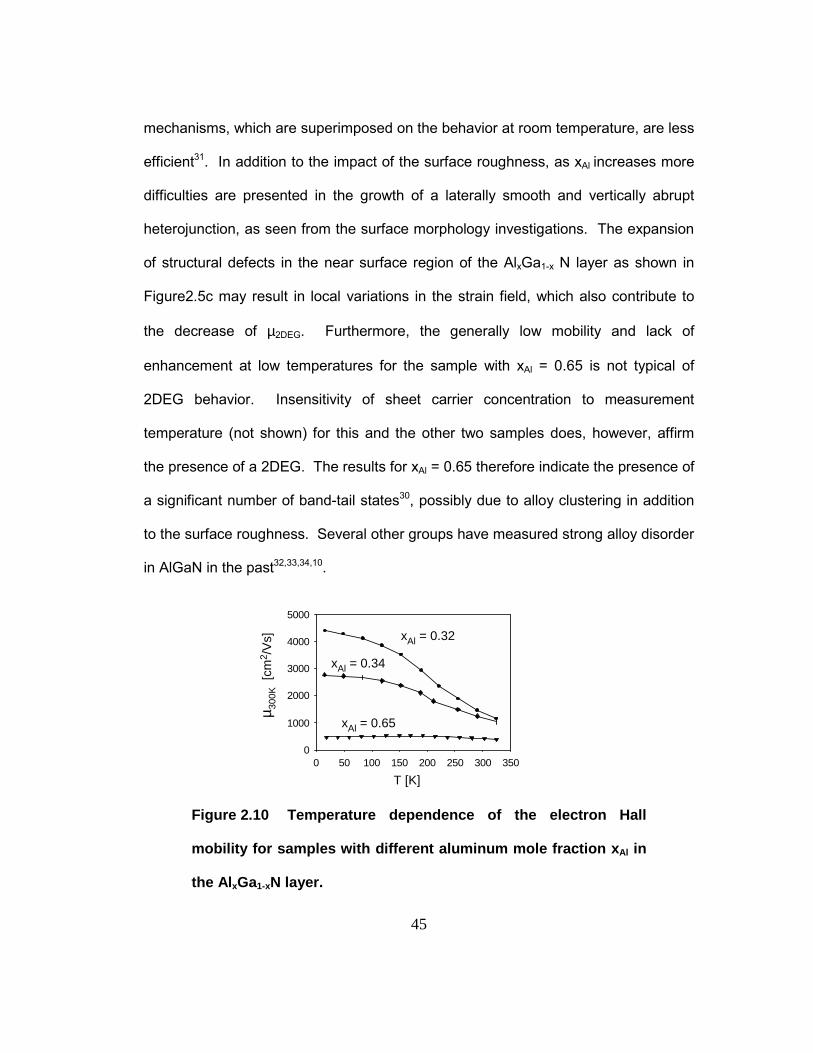
45
mechanisms, which are superimposed on the behavior at room temperature, are less
efficient31. In addition to the impact of the surface roughness, as xAl increases more
difficulties are presented in the growth of a laterally smooth and vertically abrupt
heterojunction, as seen from the surface morphology investigations. The expansion
of structural defects in the near surface region of the AlxGa1-x N layer as shown in
Figure2.5c may result in local variations in the strain field, which also contribute to
the decrease of µ2DEG. Furthermore, the generally low mobility and lack of
enhancement at low temperatures for the sample with xAl = 0.65 is not typical of
2DEG behavior. Insensitivity of sheet carrier concentration to measurement
temperature (not shown) for this and the other two samples does, however, affirm
the presence of a 2DEG. The results for xAl = 0.65 therefore indicate the presence of
a significant number of band-tail states30, possibly due to alloy clustering in addition
to the surface roughness. Several other groups have measured strong alloy disorder
in AlGaN in the past32,33,34,10.
T [K]0 50 100 150 200 250 300 350
0
1000
2000
3000
4000
5000
µ 300
K [
cm2 /
Vs]
xAl = 0.34
xAl = 0.32
xAl = 0.65
Figure 2.10 Temperature dependence of the electron Hall
mobility for samples with different aluminum mole fraction xAl in
the AlxGa1-xN layer.
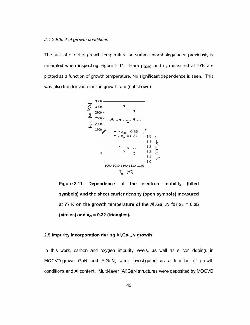
46
2.4.2 Effect of growth conditions
The lack of effect of growth temperature on surface morphology seen previously is
reiterated when inspecting Figure 2.11. Here µ2DEG and ns measured at 77K are
plotted as a function of growth temperature. No significant dependence is seen. This
was also true for variations in growth rate (not shown).
1060 1080 1100 1120 1140
0
1000
1600
2000
2400
2800
3200
3600
1.0
1.1
1.2
1.3
1.4
1.5
xAl = 0.35 xAl = 0.32
µ 77K
[cm
2 /V
s]
n s [
1013
cm
-2]
Tgr [oC]
Figure 2.11 Dependence of the electron mobility (filled
symbols) and the sheet carrier density (open symbols) measured
at 77 K on the growth temperature of the AlxGa1-xN for xAl = 0.35
(circles) and xAl = 0.32 (triangles).
2.5 Impurity incorporation during AlxGa1-xN growth
In this work, carbon and oxygen impurity levels, as well as silicon doping, in
MOCVD-grown GaN and AlGaN, were investigated as a function of growth
conditions and Al content. Multi-layer (Al)GaN structures were deposited by MOCVD
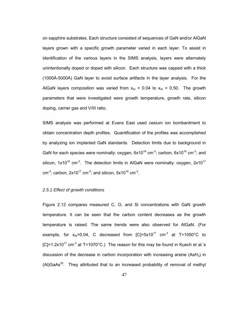
47
on sapphire substrates. Each structure consisted of sequences of GaN and/or AlGaN
layers grown with a specific growth parameter varied in each layer. To assist in
identification of the various layers in the SIMS analysis, layers were alternately
unintentionally doped or doped with silicon. Each structure was capped with a thick
(1000Å-5000Å) GaN layer to avoid surface artifacts in the layer analysis. For the
AlGaN layers composition was varied from xAl = 0.04 to xAl = 0.50. The growth
parameters that were investigated were growth temperature, growth rate, silicon
doping, carrier gas and V/III ratio.
SIMS analysis was performed at Evans East used cesium ion bombardment to
obtain concentration depth profiles. Quantification of the profiles was accomplished
by analyzing ion implanted GaN standards. Detection limits due to background in
GaN for each species were nominally: oxygen, 6x1016 cm-3; carbon, 6x1016 cm-3; and
silicon, 1x1016 cm-3. The detection limits in AlGaN were nominally: oxygen, 2x10¹⁷
cm-3; carbon, 2x1017 cm-3; and silicon, 5x1016 cm-3.
2.5.1 Effect of growth conditions
Figure 2.12 compares measured C, O, and Si concentrations with GaN growth
temperature. It can be seen that the carbon content decreases as the growth
temperature is raised. The same trends were also observed for AlGaN. (For
example, for xAl=0.04, C decreased from [C]=5x1017 cm-3 at T=1050°C to
[C]=1.2x1017 cm-3 at T=1070°C.) The reason for this may be found in Kuech et al.�s
discussion of the decrease in carbon incorporation with increasing arsine (AsH3) in
(Al)GaAs35. They attributed that to an increased probability of removal of methyl
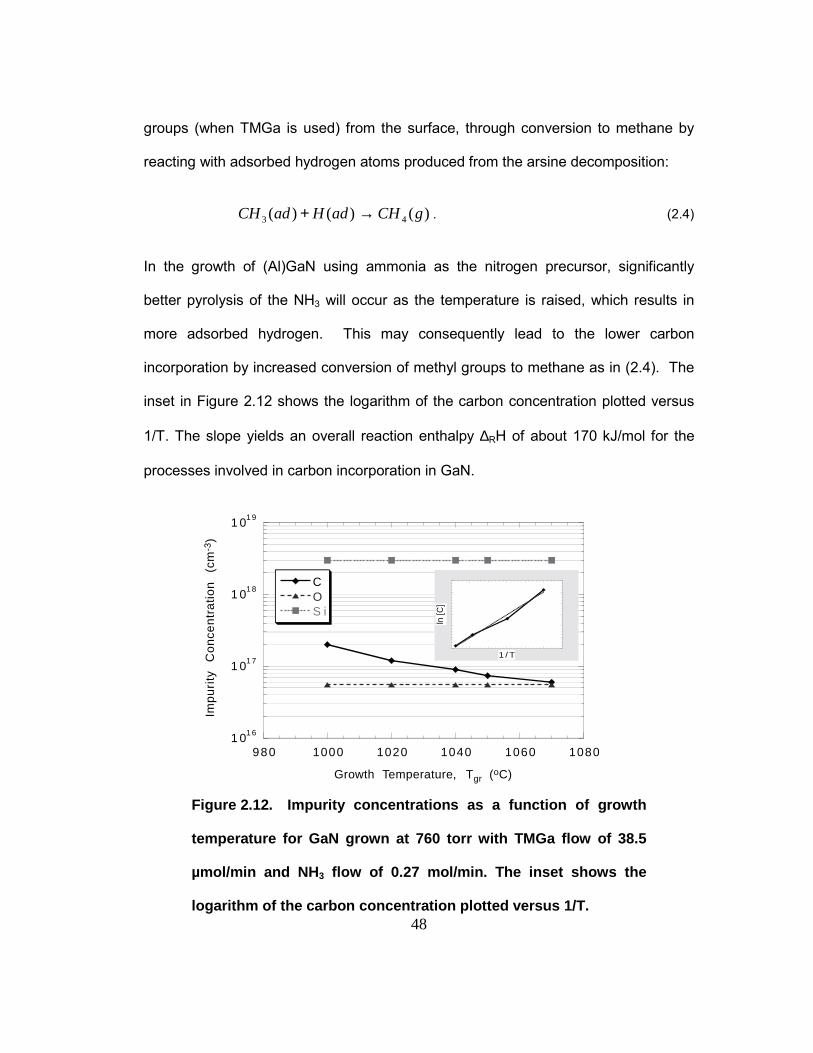
48
groups (when TMGa is used) from the surface, through conversion to methane by
reacting with adsorbed hydrogen atoms produced from the arsine decomposition:
)()()( 43 gCHadHadCH →+ . (2.4)
In the growth of (Al)GaN using ammonia as the nitrogen precursor, significantly
better pyrolysis of the NH3 will occur as the temperature is raised, which results in
more adsorbed hydrogen. This may consequently lead to the lower carbon
incorporation by increased conversion of methyl groups to methane as in (2.4). The
inset in Figure 2.12 shows the logarithm of the carbon concentration plotted versus
1/T. The slope yields an overall reaction enthalpy ∆RH of about 170 kJ/mol for the
processes involved in carbon incorporation in GaN.
1 01 6
1 01 7
1 01 8
1 01 9
980 1000 1020 1040 1060 1080
COS i
Imp
uri
ty
Co
nce
ntr
atio
n
(cm
-3)
Growth Temperature, Tgr (oC)
ln [C
]
1 / T
Figure 2.12. Impurity concentrations as a function of growth
temperature for GaN grown at 760 torr with TMGa flow of 38.5
µmol/min and NH3 flow of 0.27 mol/min. The inset shows the
logarithm of the carbon concentration plotted versus 1/T.
49
Oxygen and silicon incorporation did not appear to be affected by growth
temperature in the range investigated. However the oxygen concentrations
measured were in the vicinity of the detection limit for the SIMS and so no definitive
statement can be made. It is expected that oxygen content would decrease with
increasing temperature due to the increased volatility of the Ga2O325. The silicon
incorporation was not expected to vary with temperature due to the fact that disilane
was used as the precursor, which is known to have a constant distribution coefficient
over a wide range of growth parameters35.
Considering the previous discussion with respect to the role of the ammonia in
impurity incorporation it should come as no surprise that the impurity incorporations
are also affected by ammonia flow (V/III ratio). Figure 2.13 maps incorporation of C,
O and Si as a function of NH3 flow for GaN growth.
1 01 6
1 01 7
1 01 8
1 01 9
0 0.05 0.1 0.15 0.2 0.25 0.3
CS i
Imp
uri
ty
Co
nce
ntr
atio
n
(cm
-3)
NH3 flow, fNH3 (mol/min)
Figure 2.13 Impurity concentration as a function of NH3 flow for
GaN grown at 1070°C, 760 torr and TMGa flow of 38.5 µmol/min.
50
Once again carbon incorporation is the most strongly influenced, and decreases as
ammonia flow increases. (The apparent leveling off of this decrease at higher NH3
flows is due to the detection limits for carbon being reached and is not true behavior.)
The same trend was seen for AlGaN. (For example, for xAl=0.07, C decreased from
[C]=6x1017 cm-3 for fNH3=0.07 mol/min to [C]=1.2x1017 cm- for fNH3=0.13 mol/min.)
There are two effects to be considered with respect to the decline as ammonia flow
increases. Firstly there is the greater availability of hydrogen species for methyl
conversion, as discussed above, leading to the observed reduction. Secondly, the
increased availability of nitrogen species reduces the likelihood of formation of
nitrogen vacancies (which are the preferred carbon sites). Moreover, as the ratio of
N-species to C-species increases, the probability of forming a Ga-C bond instead of
a Ga-N bond decreases. Unfortunately the requirement of higher NH3 flow for
reduced C incorporation in AlGaN is in direct conflict with the requirement of lower
NH3 flow for improved surface morphology.
Although it appears unaffected by ammonia pressure, the level of oxygen present
was again too close to the detection limits for any firm conclusions to be drawn.
Other experiments with Al0.25Ga0.75N indicate a slight reduction in the oxygen
concentration at higher ammonia flows (from [O]=2.3x1017 cm-3 at fNH3=0.07 mol/min
to [O]=1.4x1017 cm-3 at fNH3=0.13 mol/min). It would perhaps be expected that the
amount of oxygen would increase with ammonia flow, as water in the ammonia is
believed to be one of the major sources of oxygen impurities. Obviously, however,
the competitive adsorption effect between oxygen and nitrogen dominates, similar to
the discussion above for the incorporation of carbon. That is, with an increased
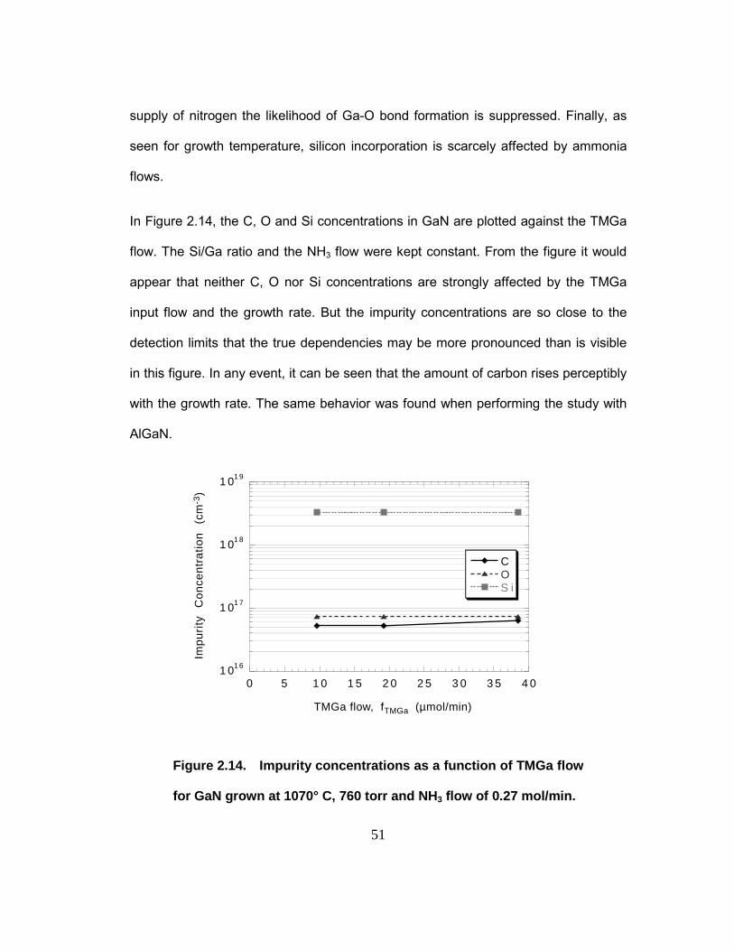
51
supply of nitrogen the likelihood of Ga-O bond formation is suppressed. Finally, as
seen for growth temperature, silicon incorporation is scarcely affected by ammonia
flows.
In Figure 2.14, the C, O and Si concentrations in GaN are plotted against the TMGa
flow. The Si/Ga ratio and the NH3 flow were kept constant. From the figure it would
appear that neither C, O nor Si concentrations are strongly affected by the TMGa
input flow and the growth rate. But the impurity concentrations are so close to the
detection limits that the true dependencies may be more pronounced than is visible
in this figure. In any event, it can be seen that the amount of carbon rises perceptibly
with the growth rate. The same behavior was found when performing the study with
AlGaN.
1 01 6
1 01 7
1 01 8
1 01 9
0 5 1 0 1 5 2 0 2 5 3 0 3 5 4 0
COS i
Imp
uri
ty
Co
nce
ntr
atio
n
(cm
-3)
TMGa flow, fTMGa (µmol/min)
Figure 2.14. Impurity concentrations as a function of TMGa flow
for GaN grown at 1070° C, 760 torr and NH3 flow of 0.27 mol/min.
52
The increase in carbon concentration is to be expected, as the methyl groups from
the TMGa are the presumed source of carbon impurities. It would also be expected
that there would be an increase in both oxygen and carbon concentrations, resulting
from the lower V/III ratio at higher group III input flows, since the NH3 flow was kept
constant for this segment of the experiment.
2.5.2 Effect of xAl
Figures 2.15a and 2.15b plot [C] and [O] against xAl. Due to the difficulty of growing
many thick AlGaN layers of different composition in one structure (cracking and
strain often make meaningful comparisons difficult, affecting especially the oxygen
incorporation), the plots combine data from several different wafers. Given the
sample-to-sample variation always present in the absolute magnitude of results from
SIMS analysis, there is a large scatter in the data. However the overall trends are
clear, that both oxygen and carbon content increase with the Al content. These
results mirror the findings of Kuech et al.35 for AlGaAs.
Due to the affinity of Al-species for oxygen36, and considering furthermore that
oxygen impurities in the TMAl precursor itself can be a contamination source, it is not
surprising that the incorporation of oxygen in the AlGaN is enhanced. The tendency
of Al to react with oxygen-bearing compounds is at least partly due to the high
stability of the oxide Al2O337.
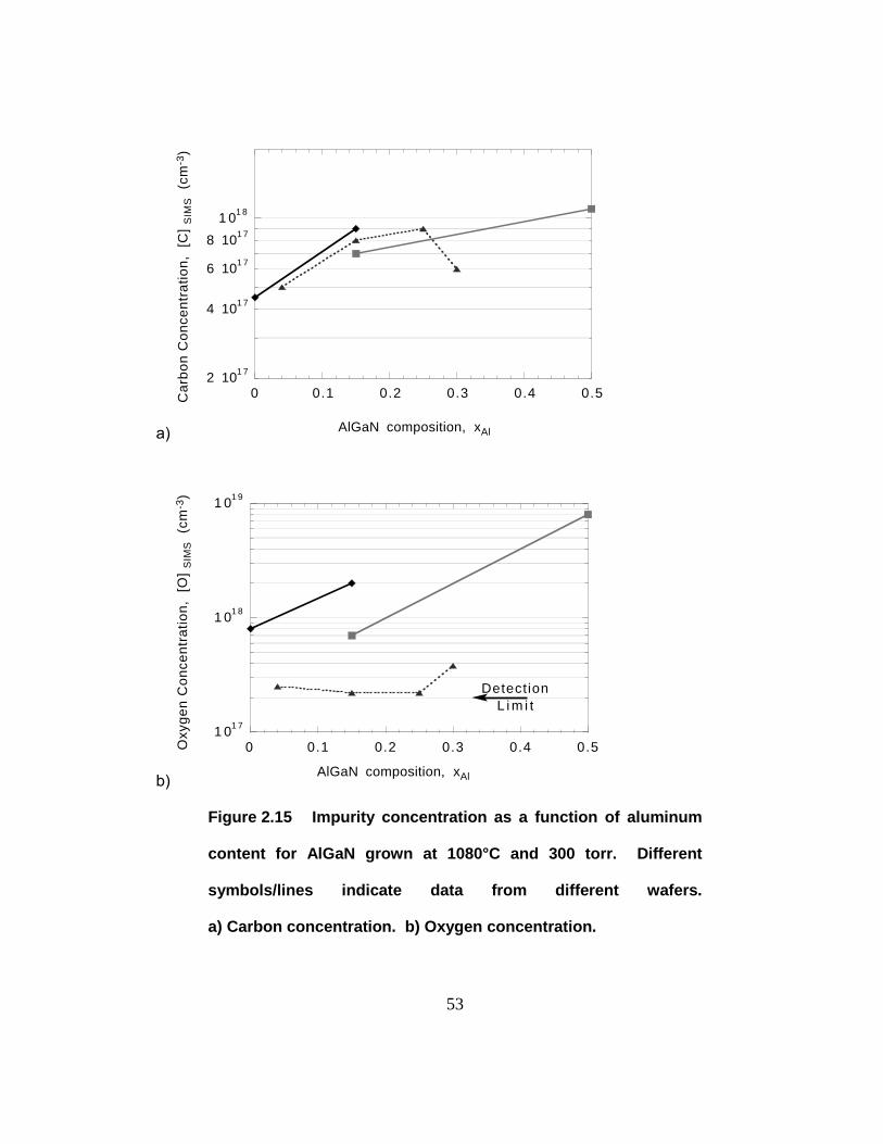
53
a)
2 101 7
4 101 7
6 101 7
8 101 7
1 01 8
0 0.1 0.2 0.3 0.4 0.5
AlGaN composition, xAl
Ca
rbo
n C
on
cen
tra
tion
, [
C]
SIM
S
(cm
-3)
b)
1 01 7
1 01 8
1 01 9
0 0.1 0.2 0.3 0.4 0.5
AlGaN composition, xAl
DetectionL i m i t
Oxy
ge
n C
on
cen
tra
tion
, [
O]
SIM
S
(cm
-3)
Figure 2.15 Impurity concentration as a function of aluminum
content for AlGaN grown at 1080°C and 300 torr. Different
symbols/lines indicate data from different wafers.
a) Carbon concentration. b) Oxygen concentration.
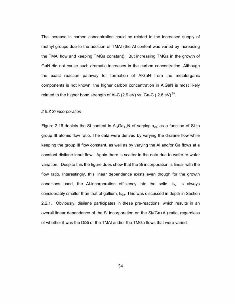
54
The increase in carbon concentration could be related to the increased supply of
methyl groups due to the addition of TMAl (the Al content was varied by increasing
the TMAl flow and keeping TMGa constant). But increasing TMGa in the growth of
GaN did not cause such dramatic increases in the carbon concentration. Although
the exact reaction pathway for formation of AlGaN from the metalorganic
components is not known, the higher carbon concentration in AlGaN is most likely
related to the higher bond strength of Al-C (2.9 eV) vs. Ga-C ( 2.6 eV) 25.
2.5.3 Si incorporation
Figure 2.16 depicts the Si content in AlxGa1-xN of varying xAl; as a function of Si to
group III atomic flow ratio. The data were derived by varying the disilane flow while
keeping the group III flow constant, as well as by varying the Al and/or Ga flows at a
constant disilane input flow. Again there is scatter in the data due to wafer-to-wafer
variation. Despite this the figure does show that the Si incorporation is linear with the
flow ratio. Interestingly, this linear dependence exists even though for the growth
conditions used, the Al-incorporation efficiency into the solid, kAl, is always
considerably smaller than that of gallium, kGa. This was discussed in depth in Section
2.2.1. Obviously, disilane participates in these pre-reactions, which results in an
overall linear dependence of the Si incorporation on the Si/(Ga+Al) ratio, regardless
of whether it was the DiSi or the TMAl and/or the TMGa flows that were varied.
55
1 01 8
1 01 9
0.01 0.1 1
x (A l )=0x(Al)=0.04x(Al)=0.15x(Al)=0.25x(Al)=0.3x(Al)=0.5
S
ilico
n C
on
cen
tra
tion
, [
Si]
SIM
S
(cm
-3)
(Si x103)/(Ga+Al)
Figure 2.16 Silicon concentration as a function of Si to group III
atomic flow ratio, for AlGaN with xAl from 0 to 0.5. Data points
were taken from many different wafers. Growth temperature was
1080°C, and flow ratio was varied by changing the DiSi flow
and/or the TMAl and/or TMGa flows.
Another, perplexing effect was observed with respect to the silicon doping of the
AlGaN. Figure 2.17 exhibits the carbon and silicon concentrations in a selected
region from one of the SIMS spectra obtained during this study. Here a small, but
distinct, step in carbon content between the doped and undoped regions of the
AlGaN is visible. Specifically, the carbon incorporation decreases in the silicon-
doped layer. This phenomenon was consistently observed in AlGaN layers of
moderate-to-high composition (15% and higher) whereas it was not detected in GaN
or Al.07Ga.93N. This effect is not well understood and clearly needs to be investigated

56
further, but may be related to the pre-reactions in the gas phase involving the TMAl
and the Si2H6.
1 01 6
1 01 7
1 01 8
1 01 9
0.5 1 1.5 2
CS i
Depth (µm)
Imp
uri
ty
Co
nce
ntr
atio
n
(cm
-3)
Figure 2.17. Selected region of SIMS results for Al.25Ga.75N,
showing carbon and silicon impurity concentrations as a
function of sputter depth.
2.6 Conclusions
Amongst the primary factors affecting the growth of AlGaN are the low mobility of Al
adatoms and high bond strength of Al to N, O and C. Due to these factors extra
measures must be taken into account for growth of AlGaN as there is an increased
tendency for defect formation compared to GaN, which is exacerbated the higher the
Al content. Growth conditions must be tailored to maximize the mobility of the
adatoms. Reduction of NH3 flows (V/III ratio) was found to be most effective for this,
although this in turn results in higher impurity (C and O) incorporation. However,
57
raising the growth temperature can help offset this effect. Thus the optimal growth
conditions (in our reactor) consisted of a NH3 flow of 1.5l/min and a growth
temperature of 1125°C. Under these conditions a growth rate on the order of 3Å/s
was suitable. Threading dislocations, besides being defects themselves, catalyze
the enhanced defect formation in AlGaN. For AlGaN layers grown on GaN the use
of reduced NH3 flows combined with growth on LEO GaN can result in a surface
morphology that is comparable to the LEO GaN.
2.7 References
1. D. Walker, X. Zhang, A. Saxler, P. Kung, J. Xu, and M. Razeghi, �Intrinsic AlxGa1-xN
detectors for the entire compositional range.� Proc SPIE 2999, 267-274 (1996)
2. S. Ruffenach-Clur, O. Briot, B. Gil, R.-. Aulombard, and J.L. Rouviere, �MOVPE
growth and structural characterization of AlxGa1-xN.� MRS Internet J. Nitride Semicond. Res.
2, 27 (1997).
3. M.D. Bremser, W.G. Perry, T. Zhevela, N.V. Edwards, O.H. Nam, N. Parikh, D.E.
Aspnes, and Robert F. Davis, �Growth, doping and characterization of AlxGa1-xN thin film
alloys on 6H-SiC(0001) substrates.� MRS Internet J. Nitride Semicond. Res. 1, 8 (1996).
4. M. Shin, A.Y. Polyakov, M. Skowronski, G.S. Rohrer, and R.G. Wilson, �Surface
defects in GaN and AlxGa1-xN epilayers deposited on sapphire by organometallic vapor phase
epitaxy.� Mat. Sci. Forum 264-268, 1251-1254 (1998).
5. W.V. Lundin, A.S. Usikov, B.V. Pushnyi, U.I. Ushakov, M.V. Stepanov, N.M. Shmidt,
T.V. Shubina, A.V. Sakharov, N.N. Faleev, V.A. Solov�ev, A.A. Sitnikova, Yu.A. Kudriavtsev,
B.Ya. Ber, and Yu.M Zadiranov, �Optical and structural studies of thick AlGaN alloy layers
and AlGaN/GaN heterostructures on sapphire substrates.� Mat. Sci. Forum 264-268, 1315-
1318 (1998).
58
6. L.J. Schowalter, J.C. Rojo, G.A. Slack, Y. Shusterman, R. Wang, I. Bhat, and G.
Arunmozhi, �Epitaxial growth of AlN and Al0.5Ga0.5N layers on aluminum nitride substrates.� J.
Cryst. Growth 211, 78-81 (2000).
7. Y. Koide, N. Itoh, K. Itoh, N. Sawaki, I. Akasaki, �Effect of AlN buffer layer on
AlGaN/α-Al2O3 heteroepitaxial growth by metalorganic vapor phase epitaxy.� Jpn. J. Appl.
Phys. 27, 1156-1161 (1988).
8. F. Omnès, N. Marenco, B. Beaumont, Ph. de Mierry, E. Monroy, F. Callè, and E.
Muñoz, �Metalorganic vapor-phase epitaxy-grown AlGaN materials for visible-blind ultraviolet
photodetector applications.�J. Appl. Phys. 86, 5287-5292 (1999).
9. J.H. Mazur, M. Benamara, Z. Liliental-Weber, W. Swider, J. Washburn, C.J.
Eiting,and R.D. Dupuis, �Effect of the doping and the Al content on the microstructure and
morphology of thin AlxGa1-xN layers grown by MOCVD.� MRS Internet J. Nitride Semicond.
Res. 5S1, W3.77 (2000).
10. K.C. Zeng, J.Y. Lin, and H.X. Jiang, �Effects of alloy disorder on the transport
properties of AlxGa1-xN epilayers probed by persistent photoconductivity.� Appl. Phys. Lett.
76, 1278-1280 (2000).
11. M. Iwaya, N. Hayashi, T. Kashima, H. Amano, and I. Akasaki, �Realization of crack-
free and high-quality thick AlxGa1-xN for UV optoelectronics using low-temperature interlayer.�
Appl. Surface Sci. 159-160, 405-413 (2000).
12. A.V. Sampath, E. Iliopoulos, K. Seth, Y. Fedyunin, H.M. Ng, P. Lamarre, Z. Feit, and
T.D. Moustakas, �GaN photodiodes grown by MBE on HVPE and ELO-HVPE GaN/sapphire
substrates.� Proc. SPIE 3948, 311-318 (2000).
13. D.J. Lambert, M.M. Wong, U. Chowdhury, C. Collins, T. Li, H.K. Kwon, B.S. Sheldon,
T.G. Zhu, J.C. Campbell, and R.D. Dupuis, �Back illuminated AlGaN solar-blind
photodetectors.� Appl. Phys. Lett. 77, 1900-1902 (2000).
14. M.D. McCluskey, C.G. Van de Walle, N.M. Johnson, D.B. Bour, and M. Kneissl, �DX
Centers in AlGaN.� Intl. J. of Mod. Phys. B13, 1363-1378 (1999).
59
15. C.G. Van de Walle, C. Stampfl, J. Neugebauer, M.D. McCluskey, and N.M. Johnson,
�Doping of AlGaN alloys.� MRS Internet J. Nitride Semicond. Res. 4S1, G10.4 (1999).
16. C. Skierbiszewski, T. Suski, M. Leszczynski, M. Shin, M. Skowronski, M.D. Bremser,
and R.F. Davis, �Evidence for localised Si-donor state and its metastable properties in
AlGaN.� Appl. Phys. Lett. 74, 3833-3835 (2000).
17. L. Akasaki and H. Amano in GaN, edited by J.I. Pankove and T.D. Moustakas
(Academic, New York, 1998) 1, 459-472.
18. O. Ambacher �Growth and applications of group III-nitrides.� J. Phys. D: Appl. Phys.
31, 2653-2710 (1998).
19. C.J. Eiting, D.J.H. Lambert, H.K. Kwon, B.S. Shelton, M.M. Wong, T.G. Zhu, and
R.P. Dupuis �Characterization of AlGaN/GaN heterostructures grown by metalorganic
chemical vapor deposition.� Phys. Stat. Sol. (b) 216, 193-197 (1999).
20. B.P. Keller, S. Keller, D. Kapolnek, W.N. Yiang, Y.-F. Wu, H. Masui, X. Wu, B.
Heying, J.S. Speck, U.K. Mishra, and S.P. DenBaars, �Metalorganic chemical vapor
deposition growth of high optical quality and high mobility GaN.� J. Electron. Mater. 24, 1707-
1709 (1995)
21. A. Thon & T. F. Kuech, �High temperature adduct formation of trimethylgallium and
ammonia.� Appl. Phys. Lett. 69; 55-57 (1996).
22. J. Han, J.J. Figiel, M.H. Crawford, M. A. Banas, M.E. Bartram, R.M. Biefeld, Y.K.
Song, and A.V. Nurmikko, �OMVPE growth and gas-phase reactions of AlGaN for UV
emitters.� J. Cryst. Growth 195, 291-296 (1998).
23. T.G. Mihopoulos, V. Gupta, and K.F. Jensen, �A reaction-transport model for AlGaN
MOVPE growth.� J. Cryst. Growth 195, 733-739 (1998).
24. F. Nakamura, S. Hashimoto, M. Hara, S. Imanaga, M. Ikeda, and H. Kawai, �AlN and
AlGaN growth using low-pressure metalorganic chemical vapor deposition.� J. Cryst. Growth
195, 280-285 (1998).
60
25. G.B. Stringfellow Organometallic Vapor-Phase Epitaxy (1989) Academic Press, San
Diego.
26. A. Koukitu, N. Takahashi, T. Taki, and H. Seki, �Thermodynamic analysis of InxGa1-xN
alloy composition grown by metalorganic vapor phase epitaxy.� Jpn. J. Appl. Phys. 35, L673-
675 (1996) A. Koukitu, N. Takahashi, and H. Seki, �Thermodynamic study on metalorganic
vapor-phase epitaxial growth of group III-nitrides.� Jpn. J. Appl. Phys. 36, L1136-1138
(1997).
27. H. Marchand, X.H. Wu, J.P. Ibbetson, P.T. Fini, P. Kozodoy, S. Keller, J.S. Speck,
S.P. DenBaars, and U.K. Mishra, �Microstructure of GaN laterally overgrown by metalorganic
chemical vapor deposition.� Appl. Phys. Lett. 73, 747-749 (1998).
28. X.H. Wu, P. Fini, E.J. Tarsa, B. Heying, S. Keller, U.K. Mishra, S.P. DenBaars, and
J.S. Speck �Dislocation generation in GaN heteroepitaxy.� J. Cryst. Growth 189/190, 231-243
(1998).
29. S. Porowski, and I. Grzegory, �Phase diagram of AlN.� Properties of Group III
Nitrides, J.P. Edgar, Ed., London: INSPEC, 1994.
30. Y. Zhang, and J. Singh, �Charge control and mobility studies for an AlGaN/GaN high
electron mobility transistor.� J. Appl. Phys. 85, 587-594 (1999).
31. L. Hsu and Walukiewicz �Electron mobility in AlxGa1-xN/GaN heterostructures.� Phys.
Rev. B 56, 1520-1528 (1997).
32. D. Korakakis, K. F. Ludwig, Jr., and T. D. Moustakas, �Long range order in AlxGa1-xN
films grown by molecular beam epitaxy.� Appl. Phys. Lett. 71, 72-74 (1997)
33. B. Neubauer, A. Rosenauer, G. Gerthsen, O. Ambacher, and M. Stutzmann,
�Analysis of composition fluctuations on an atomic scale in Al0.25Ga0.75N by high-resolution
transmission electron microscopy.� Appl. Phys. Lett. 73, 930-932 (1998)
34. A.V. Buyanov, J.A. Sandberg, B. E. Sernelius, P.O. Holtz, J.P. Bergman, B.
Monemar, H. Amano and I. Akasaki, �Photoconductivity in n-type modulation-doped
GaN/AlGaN heterostructures.� J. Cryst. Growth 189/190, 758-762 (1998)
61
35. T.F. Kuech, M.A. Tischler, R. Potemski, F. Cardone, and G. Scilla, �Doping and
dopant behavior in (Al,Ga)As grown by metalorganic vapor phase epitaxy.� J. Cryst. Growth
98, 174-187 (1989).
36. T.F. Kuech, D.J. Wolford, E. Veuhoff, V. Deline, P.M. Mooney, R. Potemski, and J.
Bradley, �Properties of high-purity AlxGa1-xAs grown by metal-organic vapor-phase-epitaxy
technique using methyl precursors.� J. Appl. Phys. 62, 632-643 (1987).
62
Chapter 3. Dislocations in GaN and their effect on p-i-n photodetectors.
As the technology for the growth of GaN has evolved, so has the knowledge of
defects, which primarily result from the inadequate substrates used. Alongside have
developed techniques to circumvent or eliminate these defects. In this chapter, the
effect of dislocations on GaN-based p-i-n photodiodes will be examined. This
particularly includes the effect of reduction of threading dislocation density (TDD) by
various substrate and overgrowth alternatives. The primary goals of the investigation
were to improve the leakage current and the cutoff characteristics of photodiodes.
3.1 Defects present in (Al)GaN
Whilst all defects, including extended and point defects (native and impurity) are of
concern for ideal photodetector performance, the high threading dislocation density
(TDD) present in GaN devices has been a primary concern in UV photodiode
development over the last 5-10 years.
3.1.1 General crystal defect theory
A fine introduction to the concept of defects is given in the book �Introduction to
Dislocations� by Derek Hull1, and is summarized here. Point defects in a crystal
occur when an atomic site is substituted or vacant, or an interstitional site is
occupied. Substitutions and interstitial defects can arise by introduction of an impurity
to the lattice or by displacement of an atom in the parent lattice from its ideal
position. Stacking faults, which are surface defects, occur when the regular
63
sequence of crystal plane stacking is interrupted. Threading dislocations - with
which this chapter is primarily concerned - are linear lattice deformations, the two
basic geometries of which are edge and screw dislocations, formed by application of
a shear stress to the lattice. Edge dislocations occur when a partial plane of atoms
is inserted into or removed from the crystal, thus displacing the atomic planes on
either side. Screw dislocations occur when part of two adjacent lattice planes are
shifted laterally with respect to each other. In many cases dislocation lines can have
a mixed edge and screw character. Finally, grain boundaries are defects formed
when a crystalline solid grows as a number of randomly oriented grains (known as a
low angle boundary when the misorientation between the grains is small and the
boundary consists of an array of dislocations), and twin boundaries occur when
adjacent planes of a crystal are mirror images of each other. Further details
regarding the basic definitions of defects can be found in Appendix A.
Due to the lattice mismatch between GaN and sapphire, true progress in epitaxial
growth of GaN was not obtained until two-step growth initiation, involving a
nucleation layer, was adopted and perfected by Amano et al2. At UCSB a low-
temperature GaN nucleation layer was developed and optimized by Keller et al.3,4,
and was used for the growth on sapphire substrates in this work. When utilizing a
nucleation layer between the substrate and the epitaxial crystal, the nucleation layer
determines the occurrence of dislocations in the epitaxial crystal5,6. Furthermore, it is
the nature of the nucleation layer after it is annealed during the temperature ramp,
which determines the growth of the high temperature GaN layer7. If nucleation
conditions result (after deposition and heating to overlayer growth temperature) in
64
large, sparse islands which coalesce to form the epitaxial film, much of the stacking
disorder manifests itself in dislocations along the basal plane which propagate
laterally. Threading dislocations are also formed, some of which (of mixed
character), are within the islands, and some of which (mostly pure edge) are formed
at the coalescence boundary of the islands. On the other hand, with a very dense
nucleation layer involving little lateral overgrowth for coalescence, the epitaxial layer
contains a huge pure edge threading dislocation density formed at the nucleation
layer grain boundaries.
Nucleation layers on SiC substrates require a different optimization, due to the
different thermal and lattice mismatch between GaN, AlN and SiC compared to
sapphire: aAl2O3 > aGaN > aAlN >aSiC and α Al2O3 > αGaN > αAlN> αSiC8. Waltereit et al.
measured strain in GaN grown on 6H-SiC with and without an AlN nucleation layer9.
The lattice mismatch introduces compressive strain, whereas cooling introduces
tensile strain. Without an AlN nucleation layer the compressive lattice mismatch
strain was relieved during growth, with the film under tension after cooling due to the
thermal mismatch, which caused cracking. With an AlN nucleation layer, which was
coherently grown, there was only a slight compressive mismatch remaining after
cool-down. Several groups have also analyzed the initial growth mechanism for
AlGaN directly deposited on SiC without a nucleation layer, and found that there is
an Al-rich layer deposited at the interface10,11. This Al-rich layer again acts to relieve
the lattice strain during growth.
In addition to the identification of the defects present in GaN, many other
experimental studies have provided insights into the consequences for electrical and
65
optical behavior. For example, scanning capacitance measurements by Hansen et
al.12 confirmed the presence of negative charge in the area surrounding dislocations.
Simultaneous scanning transmission microscopy and ballistic electron emission
microscopy measurements by Brazel et al.13 revealed the presence of localized
traps, both acceptor-like and donor-like, in the vicinity of dislocations with a screw
component. Additionally, compensation of donors in GaN:Si has been shown to
decrease with decreasing edge-type dislocation density.14 Calculations by Asbeck et
al.15 also predict piezoelectric charges resulting from the intersection of dislocations
with surfaces and interfaces.
Further defect issues such as ordering and increased defect formation, obtained with
addition of Al to GaN to form an alloy, were discussed in detail in Chapter 2.
3.1.2. Dislocation reduction techniques for GaN
As alluded to above, the characteristics of the nucleation layer strongly affect the
dislocation density in the eventual epitaxial film. For epitaxial growth of GaN with a
GaN nucleation layer, experiments at UCSB3,4 showed the importance of short
nitridation time of the sapphire as well as reduced TMGa flow to obtain an initially
rough nucleation layer prior to the temperature ramp. Several papers have also
described the benefits of depositing a thin SiN layer prior to the deposition of the
GaN nucleation layer16,17,18. Even after optimization of the nucleation layer for GaN
growth on sapphire and SiC, the TDD in the GaN is still generally in the range 108-
109 cm-3. Several groups have pioneered the use of different interlayers to further
reduce the TDD. These include use of a SiN submonolayer that modifies the surface
66
mobility of GaN layers deposited subsequently, resulting in reduction of TDD, mostly
of edge character19,20. This will be discussed in more detail later, with respect to
development of such a technique as part of this work. Amano et al. 21 have
demonstrated that the use of a low-temperature AlN layer can result in GaN and
AlGaN overlayers with fewer dislocations with a screw component. Furthermore,
several groups have reported on the annihilation of threading dislocations at
interfaces between GaN and AlGaN22 ,23.
Finally, the reduction of the TDD by LEO techniques has been well documented by
many groups, including UCSB24, with the first detailed presentation of this reduction
being a TEM study by Zheleva et al.25. Thorough experimental studies and modeling
of the effect of mask orientation and layout, as well as growth parameters, on lateral
growth rates, overgrowth profiles, and tilt in the LEO GaN have been made, and will
not be detailed here26,27,28.
3.1.3 Effects of defects on (Al)GaN photodetectors
Below is given a review of literature regarding the effect of defects on various types
of GaN and AlGaN photodetectors. The work in this chapter is principally concerned
with the effect of dislocations on photodiodes. In general, different mechanisms are
involved with photoconductors, however it is still instructive to examine the
knowledge base for defect activity in GaN-based photoconductors as well.
The most visible of issues for GaN photoconductors has been the high gain, long
response times and frequency- and optical power-dependence of the responsivity �
examples from early work were given in Chapter 1. The gain of a photoconductor is
67
given by τ=
t
gt
, in which τ is the excess-carrier recombination lifetime time and tt is
the electron transit time across the detector. (The electrons travel faster than the
holes, and can traverse the photoconductor/external circuit many times before they
recombine with the holes.) Ideally high gain is obtained as the result of a short
transit time of the electrons across the photoconductor. This requires high electron
mobility. In the case of GaN photoconductors the recombination lifetime is artificially
inflated by a long residence time of the minority carriers in traps, reducing the
probability of recombination. Thus there is a high gain but it is at the expense of a
long response time.
Many experiments have investigated the mechanisms for the long response times
and high gain, and found that acceptor levels trapping photogenerated holes were
the cause in n-type photoconductors29,30,31. Furthermore, Huang et al.32 showed that
by reducing the density of hole traps by altering growth conditions (although the
actual source of the hole trap was undetermined) response time could be reduced
and yet responsivity increased. Comparisons of GaN photoconductors grown on
sapphire and HVPE GaN templates have shown that the sharpness cutoff at the
band-edge can be improved33,34, with Redwing et al. demonstrating 7 orders of
magnitude drop in response within 20nm of the peak. With these improvements the
response times are still on the order of ms. Nobody has yet demonstrated the
behavior of GaN photoconductors in the absence of TDD such as on LEO GaN � in
the study mentioned above the HVPE GaN still had a significant TDD.
68
In photovoltaic devices it has been the direct effect of threading dislocations that has
been studied the most. Kozodoy et al.35 were the first to demonstrate the reduction
in leakage current obtained for GaN p-n structures deposited on LEO-GaN.
Following those promising results we deposited a GaN/AlGaN/GaN p-i-n solar-blind
detector structure on LEO-GaN. As well as a reduction in leakage current we
observed an improvement in response time and in sharpness of cutoff. These
results will be discussed in depth later in this chapter36. Subsequent investigations
by other groups revealed similar results with a sharper cutoff and reduced response
time and leakage current for GaN Schottky barrier photodiodes on LEO-GaN37, and a
sharper cutoff for Al0.7Ga0.3N p-i-n photodiodes on LEO-GaN (leakage currents were
not reported for those diodes)38.
In addition to the benefits of LEO, there have been other studies detailing the effect
of defects. Analysis of leakage current in GaN p-π-n photodiodes without TDD
reduction determined that it resulted from defect hopping in the π-layer39, although
the nature of the defects was not revealed. Importantly, with use of the low-
temperature AlN interlayer technique discussed above, in which mixed character but
not edge-type dislocations were eliminated, Pernot et al. recently reported that
leakage current was reduced to very low levels: 0.1nA/cm2 at a reverse bias of 10V
for AlxGa1-xN (xAl = 0 to 0.44) MSM40 photodetectors and 0.4-3.5 nA/cm2 at a reverse
bias of 5V for p-GaN/i-Al0.44Ga0.56N/n- Al0.44Ga0.56N photodiodes41. Without the
interlayer, the MSM photoconductor properties became worse (increase in response
time and PPC effects, as seen for photoconductors) as xAl was increased and the
material quality correspondingly decreased. This degradation of photodetector
69
characteristics with increasing Al content has also been observed by Monroy et al. as
a decrease in responsivity for AlxGa1-xN p-i-n photodiodes (0≤ xAl ≤0.15) 42, and as an
increase in leakage current and ideality factor and decrease in cutoff sharpness and
responsivity for AlxGa1-xN Schottky barrier photodiodes (0≤ xAl ≤ 0.35) 43.
3.1.4 Synopsis of this chapter
In this chapter several different studies of the effect of threading dislocations on
photodiode characteristics are presented. In Section 3.2 the first study looks at the
effect of different threading dislocation densities and character on GaN p-i-n diode
leakage current and spectral response. As part of this, a technique utilizing silicon
nitride/InGaN interlayers to reduce edge-type dislocation density is detailed. In
Section 3.3 leakage current in GaN p-i-n diodes with a reduced TDD is examined as
a function of electric field/intrinsic layer thickness, sidewall passivation, and diode
size/perimeter-to-area. Finally in Section 3.4 the photodetector characteristics
(leakage current, spectral response, and pulsed response) of p-GaN/i-AlGaN/n-GaN
diodes are compared with and without threading dislocation reduction.
There are several transmission electron microscopy (TEM) images presented in this
and the following chapter. The samples were prepared for TEM by wedge polishing
followed by standard Ar+ ion milling, and the images were recorded on a JEOL
2000FX microscope operated at 200kV. The AFM images were obtained using
either a Digital Instruments Nanoscope III (smaller area scans) or a Digital
Instruments D-3000 (larger area scans), both operated in tapping mode.
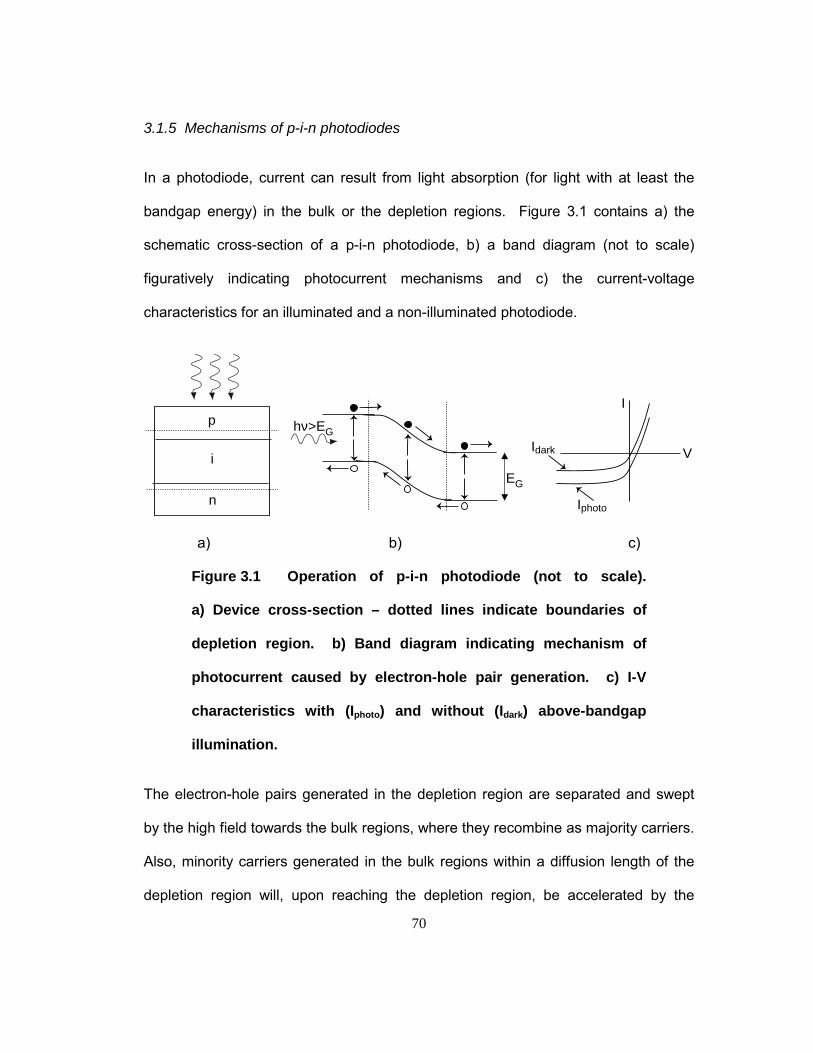
70
3.1.5 Mechanisms of p-i-n photodiodes
In a photodiode, current can result from light absorption (for light with at least the
bandgap energy) in the bulk or the depletion regions. Figure 3.1 contains a) the
schematic cross-section of a p-i-n photodiode, b) a band diagram (not to scale)
figuratively indicating photocurrent mechanisms and c) the current-voltage
characteristics for an illuminated and a non-illuminated photodiode.
EG
hν>EG
I
V
Iphoto
Idark
p
i
n
a) b) c)
Figure 3.1 Operation of p-i-n photodiode (not to scale).
a) Device cross-section – dotted lines indicate boundaries of
depletion region. b) Band diagram indicating mechanism of
photocurrent caused by electron-hole pair generation. c) I-V
characteristics with (Iphoto) and without (Idark) above-bandgap
illumination.
The electron-hole pairs generated in the depletion region are separated and swept
by the high field towards the bulk regions, where they recombine as majority carriers.
Also, minority carriers generated in the bulk regions within a diffusion length of the
depletion region will, upon reaching the depletion region, be accelerated by the
71
electric field to become majority carriers on the other side. The extension of the
depletion region by an i-region increases the ratio of drift current (a faster process) to
diffusion current. Together these two current mechanisms result in a downward shift
of the I-V curve. In general photodiodes are operated either at zero bias
(photovoltaic mode) or in reverse bias. This maximizes the difference between the
dark current and the photocurrent, and thus maximizes the sensitivity. All diodes in
this work were measured in the photovoltaic mode.
The dark current at reverse bias is referred to as the leakage current. It can result
from numerous sources in the diode. Surface leakage currents include generation
from surface states and tunneling induced near the surface. Surface leakage can be
reduced by passivation or other surface treatment that ties up dangling bonds and
thus reduces the density of surface states. Thermally generated currents include
diffusion current in the bulk regions, generation-recombination current, inter-band
and trap-to-band tunneling. Traps are expected to occur in the material as a result of
both point defects and dislocations, which are known to be present.
Figure 3.2 indicates several of these thermal mechanisms: (i) intrinsic generation, (ii)
trap-assisted generation (via deep or shallow traps), (iii) band-to-band tunneling, and
(iv) trap-assisted tunneling. As discussed for photogenerated carriers, thermally
generated carriers will contribute to leakage current if they are generated in or within
a minority carrier diffusion length of the depletion region. In reverse bias, generation
will always be the dominant process over recombination in the depletion region, but
for wide gap semiconductors such as GaN the thermal excitation rate is small. Thus

72
the diffusion and generation-recombination currents will be negligible, unless trap-
assisted.
(i) (ii)
(ii)
(iii)
(iv)
Figure 3.2 Examples of thermal generation processes in a
p-i-n diode under reverse bias. (i) Intrinsic generation, (ii) trap-
assisted generation, (iii) direct band-to-band tunneling and (iv)
trap-assisted tunneling.
3.1.6 Device layout, processing and measurements
The cross-section for a typical diode structure for the devices discussed in this
chapter is drawn in Figure 3.3a, with a photograph (surface view) of a processed
diode in Figure 3.3b. Unless otherwise specified, device fabrication consisted of the
following steps. The first step was activation of the p-layer by annealing at 950°C for
3 minutes in a N2 ambient. Device definition began with deposition of thick Pd/Au
(250Å/2000Å) p-contacts, which were annealed in N2 at 650°C for 1 minute. This
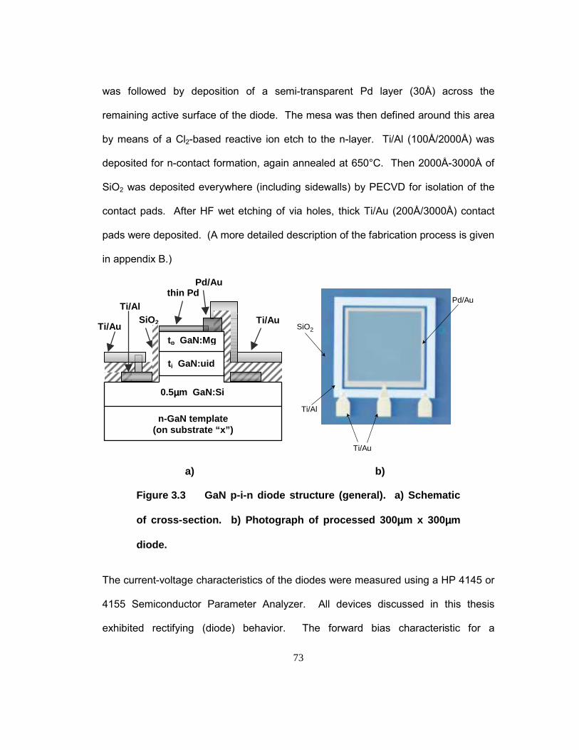
73
was followed by deposition of a semi-transparent Pd layer (30Å) across the
remaining active surface of the diode. The mesa was then defined around this area
by means of a Cl2-based reactive ion etch to the n-layer. Ti/Al (100Å/2000Å) was
deposited for n-contact formation, again annealed at 650°C. Then 2000Å-3000Å of
SiO2 was deposited everywhere (including sidewalls) by PECVD for isolation of the
contact pads. After HF wet etching of via holes, thick Ti/Au (200Å/3000Å) contact
pads were deposited. (A more detailed description of the fabrication process is given
in appendix B.)
Pd/Au
Ti/Au
Ti/Al
SiO2
a) b)
Figure 3.3 GaN p-i-n diode structure (general). a) Schematic
of cross-section. b) Photograph of processed 300µµµµm x 300µµµµm
diode.
The current-voltage characteristics of the diodes were measured using a HP 4145 or
4155 Semiconductor Parameter Analyzer. All devices discussed in this thesis
exhibited rectifying (diode) behavior. The forward bias characteristic for a
ti GaN:uid
tp GaN:Mg
Ti/Au
Pd/Au
SiO2
n-GaN template (on substrate “x”)
thin Pd
0.5µµµµm GaN:Si
Ti/Au
Ti/Al
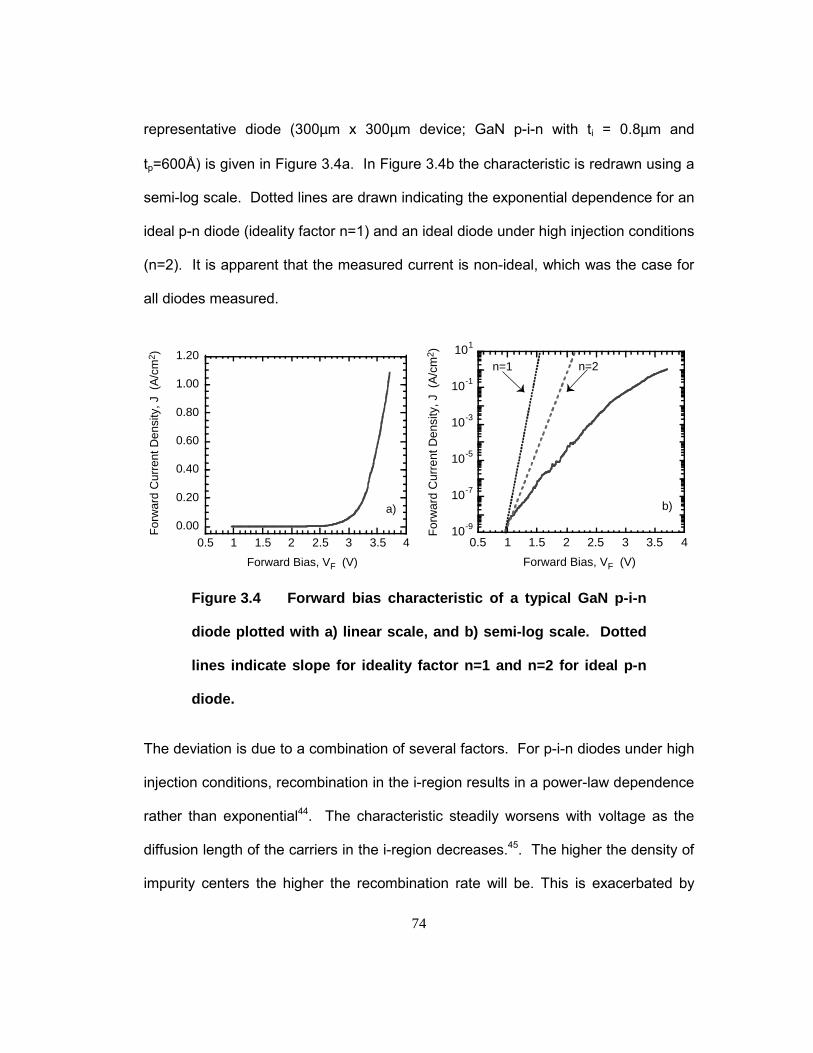
74
representative diode (300µm x 300µm device; GaN p-i-n with ti = 0.8µm and
tp=600Å) is given in Figure 3.4a. In Figure 3.4b the characteristic is redrawn using a
semi-log scale. Dotted lines are drawn indicating the exponential dependence for an
ideal p-n diode (ideality factor n=1) and an ideal diode under high injection conditions
(n=2). It is apparent that the measured current is non-ideal, which was the case for
all diodes measured.
0.00
0.20
0.40
0.60
0.80
1.00
1.20
0.5 1 1.5 2 2.5 3 3.5 4
For
war
d C
urre
nt D
ensi
ty, J
(A
/cm
2 )
Forward Bias, VF (V)
a)
10-9
10-7
10-5
10-3
10-1
101
0.5 1 1.5 2 2.5 3 3.5 4
For
war
d C
urre
nt D
ensi
ty, J
(A
/cm
2 )
Forward Bias, VF (V)
n=2n=1
b)
Figure 3.4 Forward bias characteristic of a typical GaN p-i-n
diode plotted with a) linear scale, and b) semi-log scale. Dotted
lines indicate slope for ideality factor n=1 and n=2 for ideal p-n
diode.
The deviation is due to a combination of several factors. For p-i-n diodes under high
injection conditions, recombination in the i-region results in a power-law dependence
rather than exponential44. The characteristic steadily worsens with voltage as the
diffusion length of the carriers in the i-region decreases.45. The higher the density of
impurity centers the higher the recombination rate will be. This is exacerbated by
75
Auger recombination and by carrier-carrier scattering. Also, due to the high
resistivity of the p-GaN the diodes have a high series resistance that further
degrades the characteristic. The bulk of the I-V studies presented in this and the
following chapter concern the reverse bias characteristics of the diodes, as part of
the investigations into the noise performance of the detectors.
To assess the spectral behavior of the detectors, responsivity measurements were
accomplished using a 75W xenon arc lamp, with wavelength selection using a
monochromator. A lock-in-amplifier and low-noise current pre-amplifier were used to
measure the signal, which was mechanically chopped at 310Hz. The power density
of the excitation was determined with a calibrated UV Si photodetector.
The effect of including the semi-transparent current-spreading Pd layer is shown in
Figure 3.5. 500µm x 500µm devices (GaN p-i-n with ti = 0.6µm and tp=600Å) were
fabricated with and without the 30Å Pd layer. It can be seen from the spectral
response that the device with the semi-transparent contact layer has a much higher
photocurrent. Obviously the increased current collection afforded by this contact
layer far outweighs the loss in efficiency due to absorption in the Pd (30Å Pd will
have a transmission of 75% for light of 3.4-5 eV).

76
10-4
10-3
10-2
10-1
100
101
260 280 300 320 340 360 380 400 420
with thin Pdno thin Pd
Wavelength, λ (nm)
Res
pons
ivity
, R (
norm
alis
ed)
Figure 3.5 Measured responsivity for GaN p-i-n diodes with
and without 30Å semi-transparent Pd contact layer. (normalized
to peak responsivity of diode with thin Pd layer).
3.2 Threading dislocation reduction – effect on GaN p-i-n photodiodes
In order to provide a broad investigation of the effect of threading dislocations on
photodiode leakage current and responsivity characteristics, a simple GaN p-i-n
diode structure was deposited on standard templates as well as on several templates
to which various dislocation reduction techniques had been applied. These were a
template with SiN/InGaN interlayer technique in which the density of pure edge
dislocations has been reduced, a GaN template on SiC substrate with an AlN
nucleation layer, in which the mixed character TDD is very low, and an LEO template
in which both edge and mixed TDD are significantly reduced. These are described in
77
more detail below, apart from the LEO process, which was described in Section
2.2.5.
3.2.1 XRD as a tool for TDD comparison
Whilst TEM measurements are time-consuming and expensive, XRD measurements
are a fast and convenient method for assessment of the TD density and makeup in
films. Heying et al.46 demonstrated the correlation between FWHM values of rocking
curves both on-and off-axis with the edge and mixed components of the TDD in
GaN. For GaN films grown on (0001) sapphire, as is the case here, the (0002)
planes are not distorted by edge-type dislocations in the [0001] line directions, and
the (0002) rocking curves are only sensitive to the screw TD content in the films (this
includes mixed character TD�s). On the other hand, the (10 12) and the (20 21)
rocking curve peaks are broadened by TD�s with either screw or edge character.
Srikant et al. modeled this for epitaxial films that consist of a mosaic structure of
slightly misoriented sub-grains47 (this includes GaN on sapphire). Their model
demonstrated that the sensitivity towards the tilt of the subgrains increases, the
closer the inclination is to being in-plane. Thus the (2021) rocking curve, at angle of
70° to the axis, will mostly reflect the pure edge TDD. They also point out, though,
that the mosaic character determined by the XRD will only include dislocation
networks that result in a misorientation between the film and the substrate. However
some edge-type dislocations will result in aligned subgrains and therefore have no
effect on the tilt and twist of the subgrains, i.e. the mosaic.
78
3.2.2 SiN/InGaN interlayer technique for TDD reduction
A method of dislocation reduction utilizing a submonolayer of silicon nitride (SixNy)
was developed as part of this work. This involved selective island growth of thin
InGaN layers on top of the SixNy. (In other work at UCSB, InGaN islands had been
observed to grow in a spiral growth mode around threading dislocations with a screw
component after partial passivation of the GaN surface with SixNy48.) SixNy was
deposited on top of a standard GaN template at the same temperature as the GaN
(1070°C) by flowing NH3 and DiSi. Then a 12nm thick In0.1Ga0.9N layer was
deposited at 790°C, followed by another GaN layer at 1070°C. This was repeated
either two or four times. The SixNy layer was either 0.07 or 0.14 Å.
Figure 3.6 indicates the results of XRD measurements for the different combinations
of interlayers. If the model of Srikant et al.47 is valid for the dislocations in the
overgrown layers (if they affect the mosaic), the off-axis XRD FWHM values (shown
here in units of arc-seconds) reveal a decrease in TDD compared to the underlying
templates. In Figure 3.6a, samples without, with two, and with four interlayers are
compared to study the effect of the number of interlayers. The underlying GaN
template was 0.5µm, with 0.5µm between interlayers, and the total thickness after
capping with GaN was kept constant at 3µm. The (0002) FWHM values were
relatively unaffected by the number of interlayers, indicating the TDD with a screw
component is unchanged. However, the (10 12) FWHM changes with the number of
interlayers. Whilst the first two interlayers resulted in a decrease in the (10 12)
FWHM, an increase to four interlayers caused it to increase again.

79
300
400
500
600
700
800
900
0 1 2 3 4 5
002102
Number of SixNy/InGaN interlayers
FW
HM
XR
D (
arcs
ec)
250
300
350
400
450
500
550
600
0.06 0.08 0.1 0.12 0.14 0.16
002102
SixNy thickness, d (Å)
FW
HM
XR
D (
arcs
ec)
a) b)
Figure 3.6. FWHM of the (0002) and (10 12) diffraction peaks
for samples with silicon nitride/InGaN interlayers with a) different
number of interlayers and b) different silicon nitride thickness.
In Figure 3.6b, samples with a SixNy thickness of 0.07Å and 0.14Å are compared.
For these wafers the underlying GaN template was 3µm, with 0.5µm GaN between
two interlayers, and a GaN cap thickness of 2.5µm. (Note that the thicker underlying
template results in an overall reduced TDD compared to the wafers in Fig 3.6a.)
Here it can be seen that increasing the thickness of the SixNy layer results in a lower
(10 12) FWHM. Other experiments utilizing this technique for GaN on Si revealed
that increasing the thickness beyond 0.14Å was again detrimental. Thus the
template used in the photodetector study to be described below utilized two (on a
2µm thick GaN template) with a nitride thickness of 0.14Å. This combination had the
lowest (10 12) FWHM and thus, if the mosaic model applies, the lowest edge-type
TDD of the above wafers. Preliminary TEM studies were inconclusive as to the
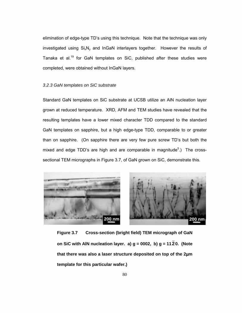
80
elimination of edge-type TD�s using this technique. Note that the technique was only
investigated using SixNy and InGaN interlayers together. However the results of
Tanaka et al.19 for GaN templates on SiC, published after these studies were
completed, were obtained without InGaN layers.
3.2.3 GaN templates on SiC substrate
Standard GaN templates on SiC substrate at UCSB utilize an AlN nucleation layer
grown at reduced temperature. XRD, AFM and TEM studies have revealed that the
resulting templates have a lower mixed character TDD compared to the standard
GaN templates on sapphire, but a high edge-type TDD, comparable to or greater
than on sapphire. (On sapphire there are very few pure screw TD�s but both the
mixed and edge TDD�s are high and are comparable in magnitude5.) The cross-
sectional TEM micrographs in Figure 3.7, of GaN grown on SiC, demonstrate this.
200 nm 200 nm
Figure 3.7 Cross-section (bright field) TEM micrograph of GaN
on SiC with AlN nucleation layer. a) g = 0002, b) g = 1120. (Note
that there was also a laser structure deposited on top of the 2µµµµm
template for this particular wafer.)
81
In Figure 3.7a, g=0002 and only mixed and screw TD�s will be visible. In figure 3.7b,
g=11 20 and only mixed and edge TD�s will be visible. It is therefore obvious from
the significantly higher number of TD�s visible in Figure 3.7b that the edge-type TDD
is high but the mixed character TDD is low.
The GaN template on SiC used in the photodetector study to be described below
was grown under similar conditions to the template shown in Figure 3.7. It had a
750Å low temperature AlN nucleation layer, followed by a 750Å grade to GaN and
then the high-temperature GaN epitaxial layer.
3.2.4 TDD comparison (by XRD) for the template study
Figure 3.8 compares the FWHM (shown here in units of arc-seconds) of the on- and
off-axis diffraction peaks for four of the five wafers used in this study. These
measurements were made after these wafers had identical GaN p-i-n structures
deposited on each of them. The peak widths are plotted against the inclination angle
during the XRD measurement, with extrapolation to an angle of 90° to indicate the
pure edge component of the TDD. The FWHM for the LEO GaN template is not
shown, as the diffraction peaks in that case were broadened by tilt in the underlying
wings and not indicative of the true (low) TDD. The wafer indicated as �highly
dislocated� was a template that was not grown under fully optimized conditions, and
had a higher TDD than usual.
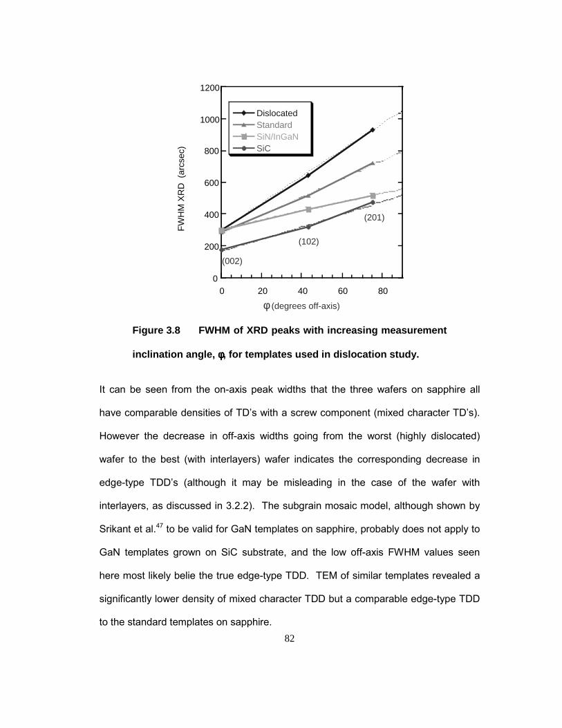
82
0
200
400
600
800
1000
1200
0 20 40 60 80
DislocatedStandardSiN/InGaNSiC
φ (degrees off-axis)
(102)
(201)
(002)
FW
HM
XR
D (
arcs
ec)
Figure 3.8 FWHM of XRD peaks with increasing measurement
inclination angle, φφφφ, for templates used in dislocation study.
It can be seen from the on-axis peak widths that the three wafers on sapphire all
have comparable densities of TD�s with a screw component (mixed character TD�s).
However the decrease in off-axis widths going from the worst (highly dislocated)
wafer to the best (with interlayers) wafer indicates the corresponding decrease in
edge-type TDD�s (although it may be misleading in the case of the wafer with
interlayers, as discussed in 3.2.2). The subgrain mosaic model, although shown by
Srikant et al.47 to be valid for GaN templates on sapphire, probably does not apply to
GaN templates grown on SiC substrate, and the low off-axis FWHM values seen
here most likely belie the true edge-type TDD. TEM of similar templates revealed a
significantly lower density of mixed character TDD but a comparable edge-type TDD
to the standard templates on sapphire.
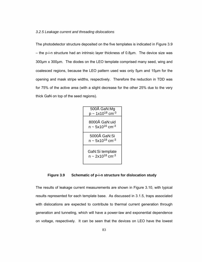
83
3.2.5 Leakage current and threading dislocations
The photodetector structure deposited on the five templates is indicated in Figure 3.9
� the p-i-n structure had an intrinsic layer thickness of 0.8µm. The device size was
300µm x 300µm. The diodes on the LEO template comprised many seed, wing and
coalesced regions, because the LEO pattern used was only 5µm and 15µm for the
opening and mask stripe widths, respectively. Therefore the reduction in TDD was
for 75% of the active area (with a slight decrease for the other 25% due to the very
thick GaN on top of the seed regions).
500Å GaN:Mgp ~ 1x1018 cm-3
8000Å GaN:uidn ~ 5x1016 cm-3
GaN:Si templaten ~ 2x1018 cm-3
5000Å GaN:Sin ~ 5x1018 cm-3
Figure 3.9 Schematic of p-i-n structure for dislocation study
The results of leakage current measurements are shown in Figure 3.10, with typical
results represented for each template base. As discussed in 3.1.5, traps associated
with dislocations are expected to contribute to thermal current generation through
generation and tunneling, which will have a power-law and exponential dependence
on voltage, respectively. It can be seen that the devices on LEO have the lowest
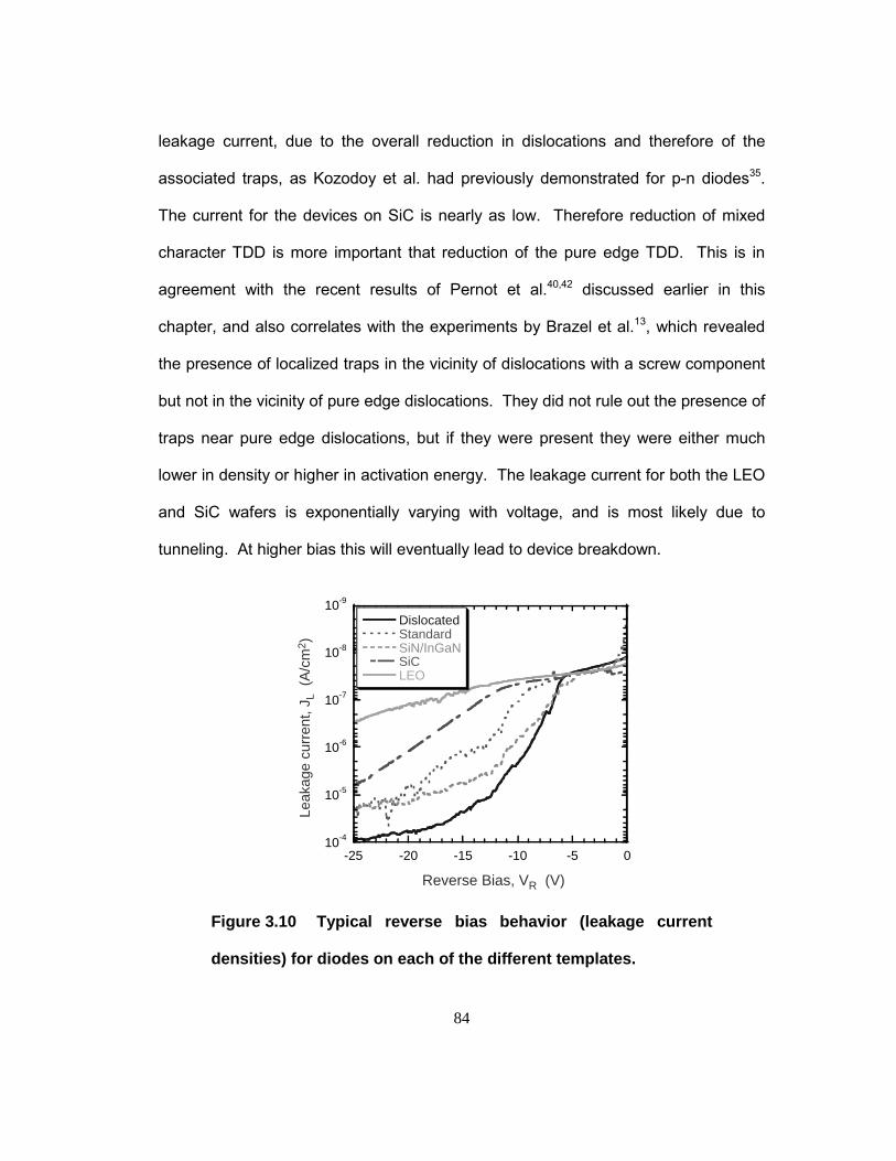
84
leakage current, due to the overall reduction in dislocations and therefore of the
associated traps, as Kozodoy et al. had previously demonstrated for p-n diodes35.
The current for the devices on SiC is nearly as low. Therefore reduction of mixed
character TDD is more important that reduction of the pure edge TDD. This is in
agreement with the recent results of Pernot et al.40,42 discussed earlier in this
chapter, and also correlates with the experiments by Brazel et al.13, which revealed
the presence of localized traps in the vicinity of dislocations with a screw component
but not in the vicinity of pure edge dislocations. They did not rule out the presence of
traps near pure edge dislocations, but if they were present they were either much
lower in density or higher in activation energy. The leakage current for both the LEO
and SiC wafers is exponentially varying with voltage, and is most likely due to
tunneling. At higher bias this will eventually lead to device breakdown.
10-9
10-8
10-7
10-6
10-5
10-4
-25 -20 -15 -10 -5 0
DislocatedStandardSiN/InGaNSiCLEO
Reverse Bias, VR (V)
Leak
age
curr
ent,
J L (
A/c
m2 )
Figure 3.10 Typical reverse bias behavior (leakage current
densities) for diodes on each of the different templates.
85
The smaller influence of edge-type TD�s is also indicated by comparison of the
leakage currents for the devices on the SiN/InGaN-interlayer, standard, and highly
dislocated template bases. There was some variation between devices within each
wafer, but in general the devices on the highly dislocated devices had the highest
leakage current, while the devices on the SiN/InGaN interlayer template had at best
the same leakage current as those on the standard template, and on average slightly
worse. It is apparent that at very high densities the presence edge-type TD�s
(dislocated wafer) do contribute significantly to leakage current, and reduction to the
moderately high TDD in the standard wafer results in an improvement. However,
further reduction of edge-type TDD beyond these levels (SiN/InGaN wafer) has little
or no effect, once again indicating there is less trap-assisted current associated with
the edge-type TD�s. However, it may also be an indication that the XRD
measurements were indeed misleading regarding the occurrence of TDD reduction
using the SiN/InGaN interlayers.
Another feature to note is the uneven behavior exhibited by devices from those three
wafers on GaN/sapphire templates. Some (although not all) devices from each of
these wafers produced this behavior, where the leakage current increases sharply,
and then saturates again. Contrast between the low field and the high field behavior
has been observed by others for GaN p-n junctions. Kuksenkov et al. attributed the
behavior they witnessed at lower fields to carrier hopping between traps49. Sampath
et al. attributed an initial steep increase in leakage current to a detrapping of donor
levels, which were all emptied at larger reverse bias50. This may be the situation
here, with donor levels associated with the mixed character TD�s present in the
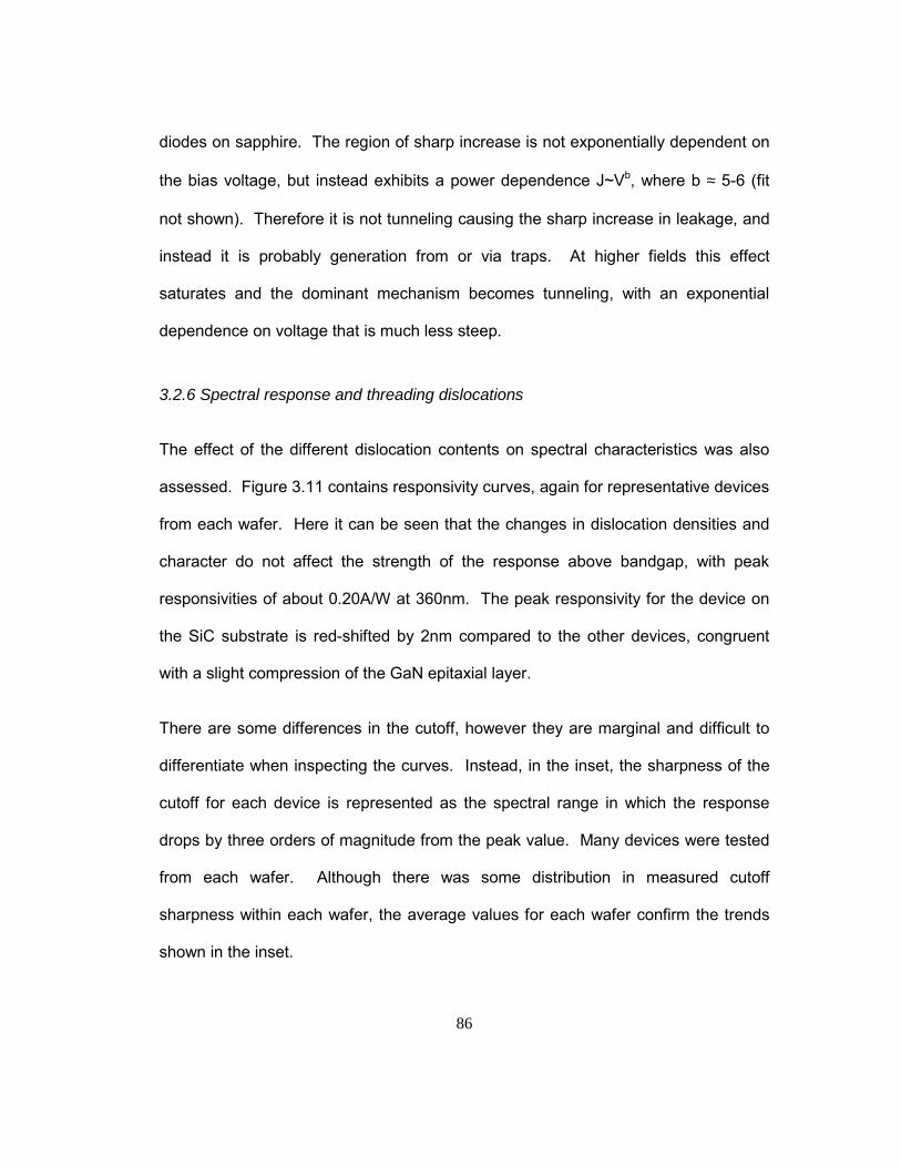
86
diodes on sapphire. The region of sharp increase is not exponentially dependent on
the bias voltage, but instead exhibits a power dependence J~Vb, where b ≈ 5-6 (fit
not shown). Therefore it is not tunneling causing the sharp increase in leakage, and
instead it is probably generation from or via traps. At higher fields this effect
saturates and the dominant mechanism becomes tunneling, with an exponential
dependence on voltage that is much less steep.
3.2.6 Spectral response and threading dislocations
The effect of the different dislocation contents on spectral characteristics was also
assessed. Figure 3.11 contains responsivity curves, again for representative devices
from each wafer. Here it can be seen that the changes in dislocation densities and
character do not affect the strength of the response above bandgap, with peak
responsivities of about 0.20A/W at 360nm. The peak responsivity for the device on
the SiC substrate is red-shifted by 2nm compared to the other devices, congruent
with a slight compression of the GaN epitaxial layer.
There are some differences in the cutoff, however they are marginal and difficult to
differentiate when inspecting the curves. Instead, in the inset, the sharpness of the
cutoff for each device is represented as the spectral range in which the response
drops by three orders of magnitude from the peak value. Many devices were tested
from each wafer. Although there was some distribution in measured cutoff
sharpness within each wafer, the average values for each wafer confirm the trends
shown in the inset.
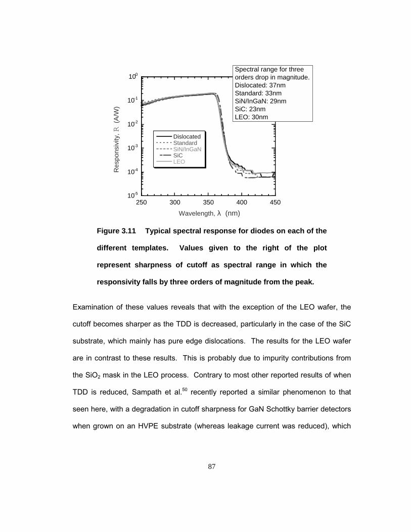
87
10-5
10-4
10-3
10-2
10-1
100
250 300 350 400 450
DislocatedStandardSiN/InGaNSiCLEO
Res
pons
ivity
, R (
A/W
)
Wavelength, λ (nm)
Spectral range for three orders drop in magnitude.Dislocated: 37nmStandard: 33nmSiN/InGaN: 29nmSiC: 23nmLEO: 30nm
Figure 3.11 Typical spectral response for diodes on each of the
different templates. Values given to the right of the plot
represent sharpness of cutoff as spectral range in which the
responsivity falls by three orders of magnitude from the peak.
Examination of these values reveals that with the exception of the LEO wafer, the
cutoff becomes sharper as the TDD is decreased, particularly in the case of the SiC
substrate, which mainly has pure edge dislocations. The results for the LEO wafer
are in contrast to these results. This is probably due to impurity contributions from
the SiO2 mask in the LEO process. Contrary to most other reported results of when
TDD is reduced, Sampath et al.50 recently reported a similar phenomenon to that
seen here, with a degradation in cutoff sharpness for GaN Schottky barrier detectors
when grown on an HVPE substrate (whereas leakage current was reduced), which

88
they attributed to band tail states associated with the high background carrier
concentration in the HVPE GaN.
3.3 Sources of leakage current in the case of reduced TDD
With threading dislocations confirmed as a major contributor to the leakage current in
the p-i-n diodes, we further investigated the source of the remaining leakage current
in the absence of threading dislocations. To that end a series of GaN p-i-n diodes
was deposited on LEO wafers. For this series, the thickness of the i-layer was varied
from 1300Å to 1 µm.
3.3.1 High-quality coalescence of LEO
For these wafers, an improved LEO growth technique was used. Fini et al51 had
developed a two-step technique for LEO coalescence to minimize tilt in the wings,
which consequently reduced the formation of dislocations at the coalescence
boundary. Furthermore, wafers grown by this technique also exhibited a low TDD
above the mask window, presumably due to the thickness of the GaN.
3.3.2 Leakage current and intrinsic layer thickness
In this study, GaN p-i-n diodes were deposited and fabricated in essentially the same
manner as for the previous study involving different templates. Three wafers were
grown, with intrinsic layer thickness of 1000Å, 5000Å and 10,000Å (the thickness
varied across the wafer area � actual thickness in the area in which the diodes were
measured has been taken into account in analysis of the results). In order to also

89
establish any perimeter or volume dependence of the leakage current, three diode
sizes were used: 300µm x 300µm, 150µm x 600µm, and 500µm x 500µm.
Figure 3.12 compares the leakage currents for 300µm x 300µm devices from each
wafer. In order to make a valid comparison, the current is plotted as a function of
electric field in the depletion region. It can be seen here that the leakage current
becomes worse at a given field for larger values of ti. This trend indicates that traps
due to defects in the i-layer are the cause of the leakage current in the absence of
threading dislocations. The intrinsic layer is formed by compensation of the
unintentional n-type doping. This is achieved by growing the GaN under those
conditions that favor increased impurity incorporation. Consequently it is a
straightforward conclusion that the traps causing leakage current in the absence of a
large TDD are associated with point defects.
10-8
10-7
10-6
10-5
10-4
10-3
10-2
-2.5 -2 -1.5 -1 -0.5 0
ti=0.15µmti=0.59µmti=0.96µm
Reverse Bias Field, ER (MV/cm)
Leak
age
curr
ent,
J L (
A/c
m2 )
Figure 3.12 Leakage current density plotted against the reverse
applied field for GaN p-i-n diodes with different intrinsic layer
thickness, ti.
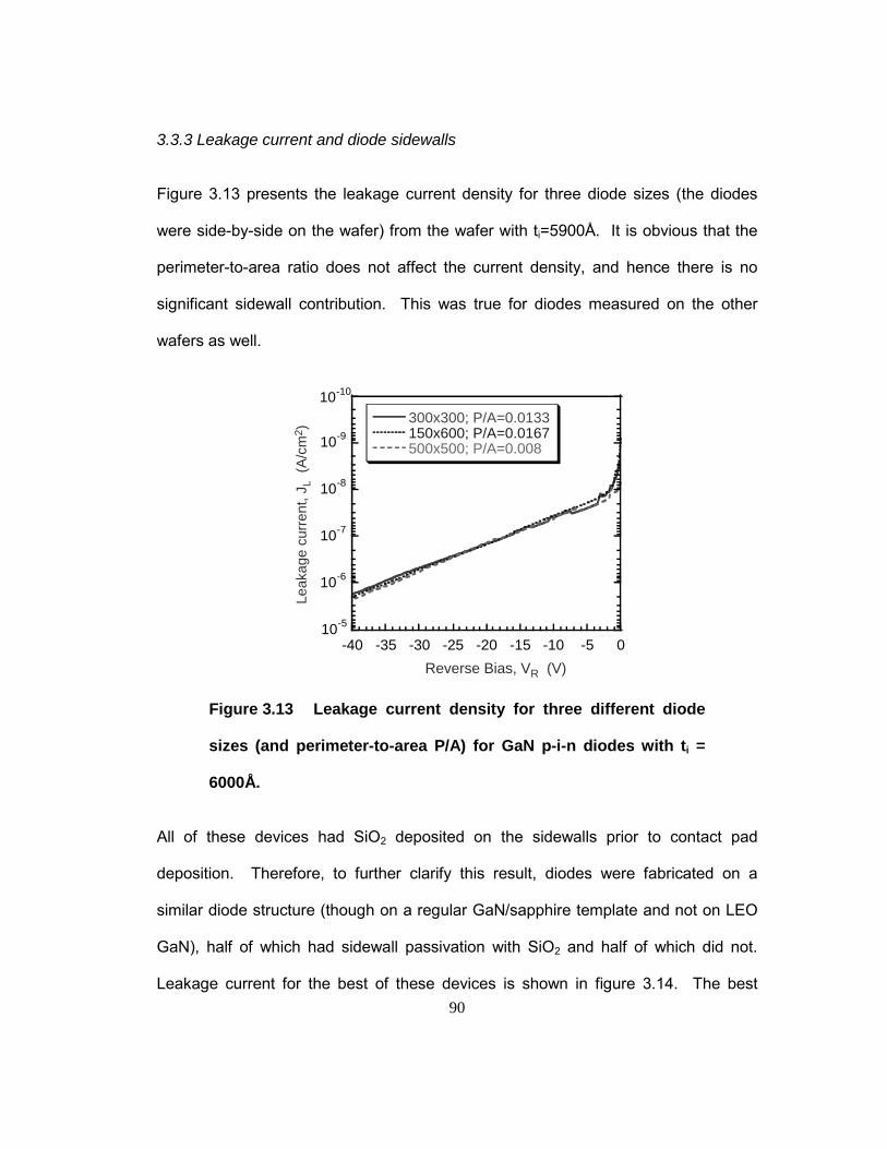
90
3.3.3 Leakage current and diode sidewalls
Figure 3.13 presents the leakage current density for three diode sizes (the diodes
were side-by-side on the wafer) from the wafer with ti=5900Å. It is obvious that the
perimeter-to-area ratio does not affect the current density, and hence there is no
significant sidewall contribution. This was true for diodes measured on the other
wafers as well.
Leak
age
curr
ent,
J L (
A/c
m2 )
Reverse Bias, VR (V)
10-10
10-9
10-8
10-7
10-6
10-5
-40 -35 -30 -25 -20 -15 -10 -5 0
300x300; P/A=0.0133150x600; P/A=0.0167500x500; P/A=0.008
Figure 3.13 Leakage current density for three different diode
sizes (and perimeter-to-area P/A) for GaN p-i-n diodes with ti =
6000Å.
All of these devices had SiO2 deposited on the sidewalls prior to contact pad
deposition. Therefore, to further clarify this result, diodes were fabricated on a
similar diode structure (though on a regular GaN/sapphire template and not on LEO
GaN), half of which had sidewall passivation with SiO2 and half of which did not.
Leakage current for the best of these devices is shown in figure 3.14. The best
91
devices without SiO2 are as good as the best devices with SiO2. It is apparent that
even in the presence of a high dislocation density (without LEO template) the
sidewall passivation using SiO2 does not affect the leakage current.
10-9
10-8
10-7
10-6
10-5
10-4
10-3
-35 -30 -25 -20 -15 -10 -5 0
passivatednonpassivated
Leak
age
curr
ent,
J L (
A/c
m2 )
Reverse Bias, VR (V)
Figure 3.14 Leakage current density for 150µµµµm x 600 µµµµm p-i-n
diodes fabricated with and without sidewall passivation by SiO2
deposition. These were the best diodes measured. For these
diodes ti = 6000Å and a standard GaN template was used.
A further outcome of these experiments is that measurements revealed, in some
cases, diodes with massive leakage in both the forward and reverse directions. The
reason for why this occurred could be processing-related, possibly due to metal
migration through the junction when the contacts were annealed. On some wafers
few to none of the devices exhibited such behavior, on other wafers many did and
many devices had to be tested to find diodes without such chronic leakage in order
to obtain valid comparisons between the wafers.
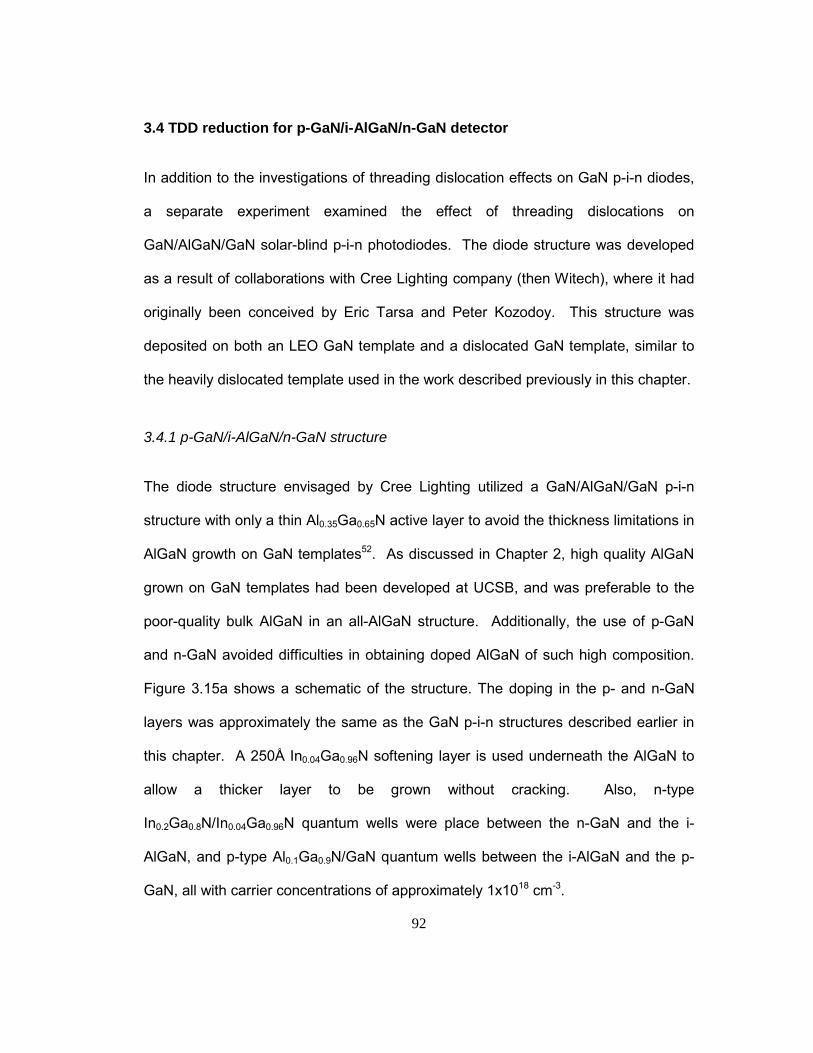
92
3.4 TDD reduction for p-GaN/i-AlGaN/n-GaN detector
In addition to the investigations of threading dislocation effects on GaN p-i-n diodes,
a separate experiment examined the effect of threading dislocations on
GaN/AlGaN/GaN solar-blind p-i-n photodiodes. The diode structure was developed
as a result of collaborations with Cree Lighting company (then Witech), where it had
originally been conceived by Eric Tarsa and Peter Kozodoy. This structure was
deposited on both an LEO GaN template and a dislocated GaN template, similar to
the heavily dislocated template used in the work described previously in this chapter.
3.4.1 p-GaN/i-AlGaN/n-GaN structure
The diode structure envisaged by Cree Lighting utilized a GaN/AlGaN/GaN p-i-n
structure with only a thin Al0.35Ga0.65N active layer to avoid the thickness limitations in
AlGaN growth on GaN templates52. As discussed in Chapter 2, high quality AlGaN
grown on GaN templates had been developed at UCSB, and was preferable to the
poor-quality bulk AlGaN in an all-AlGaN structure. Additionally, the use of p-GaN
and n-GaN avoided difficulties in obtaining doped AlGaN of such high composition.
Figure 3.15a shows a schematic of the structure. The doping in the p- and n-GaN
layers was approximately the same as the GaN p-i-n structures described earlier in
this chapter. A 250Å In0.04Ga0.96N softening layer is used underneath the AlGaN to
allow a thicker layer to be grown without cracking. Also, n-type
In0.2Ga0.8N/In0.04Ga0.96N quantum wells were place between the n-GaN and the i-
AlGaN, and p-type Al0.1Ga0.9N/GaN quantum wells between the i-AlGaN and the p-
GaN, all with carrier concentrations of approximately 1x1018 cm-3.
93
sapphire
e-
EG(AlGaN)> hν > EG(GaN)
EG(AlGaN)EG(GaN)
EG(GaN)hν
h+
3000Å GaN:Si
250Å In.04Ga.96N:Si
500Å Al.33Ga.67N:uid
80Å GaN:Mg
GaN template
2xQW30Å GaN:Mg/
50Å Al.1GaN.9:Mg
2xQW30Å In.2Ga.8N:Mg/60Å In.04GaN.96:Si
a) b)
Figure 3.15 p-GaN/i-AlGaN/n-GaN solar-blind detector.
a) Schematic of device structure. b) Band diagram (not to scale)
of structure in the absence of the quantum well barrier layers,
indicating potential for photogenerated electrons and holes from
GaN regions to reach AlGaN and contribute to photocurrent.
In Figure 3.15b the band diagram is indicated for such a structure but without the
quantum wells. The barrier between the AlGaN and the p- and n- (In)GaN layers is
very important. Figure 3.15b indicates how photogenerated holes in the n-GaN and
electrons in the p-GaN could surmount ∆Ev and ∆Ec, respectively, between the GaN
and AlGaN. Thus for impinging light with EG(AlGaN)>hν>EG(GaN) there may be
photocurrent due to these which detracts from solar-blind cutoff properties of the
AlGaN i-layer. Fortunately, the polarization in GaN/AlGaN/GaN structures grown by
94
MOCVD on sapphire augments the barrier provided by the energy gap
discontinuities. As discussed in relation to AlGaN/GaN HEMTs in the introductory
chapter, the polarization induces a large electric field at the AlGaN/GaN interface for
AlGaN layers on GaN/sapphire grown by MOCVD. Similarly there will be
polarization charge at the upper GaN/AlGaN interface resulting in a large field of the
opposite sign at that interface. These fields result in an enhancement of the barriers
to minority carriers from the p- and n- regions. The quantum wells provide an
additional high-recombination region to further prevent unwanted carrier movement.
Simulations by Pulfrey et al.53 confirmed the beneficial effect of the quantum wells.
3.4.2 TDD study
The photodetector p-i-n structures were deposited by MOCVD on the LEO and
dislocated GaN templates, which had been previously grown. XRD measurements
revealed the composition of the AlGaN layer to be 33% Al. On the LEO GaN wafer,
10µm x 1000µm mesas were defined so that the active area was entirely contained
within the LEO wings. For comparison, 30µm x 1000µm mesas were defined, that
additionally spanned the coalesced region between two wings. For both of these
diode layouts the active area did not incorporate any of the dislocated seed regions.
A photograph of the finished diodes, showing alignment with the underlying LEO
pattern, is given in Figure 3.16. Square 300µm x 300µm mesas were defined on the
dislocated GaN wafer. In this experiment there was sidewall passivation and large
pad deposition only for the devices on LEO, and there was no thin Pd layer on any of
the devices.

95
wing only
across coalescence
seed stripes
coalescence stripes
Figure 3.16 Diodes on LEO GaN template after completion of
processing. The LEO pattern is visible under the diodes, which
were fabricated both on the wing-only regions and spanning the
coalescence region.
3.4.3 Leakage current and threading dislocations
Again, reverse-bias current measurements showed that dislocation reduction
resulted in a reduction in leakage current. Leakage currents for the various types of
diode are plotted in Figure 3.17. The diodes fabricated on the wing region only of the
LEO GaN exhibit extremely low current densities of 10 nA/cm2 at a reverse bias of �
5V. At that bias the diodes with the active area encompassing the coalescence
region had a leakage current density of 100 nA/cm2, an order of magnitude higher.
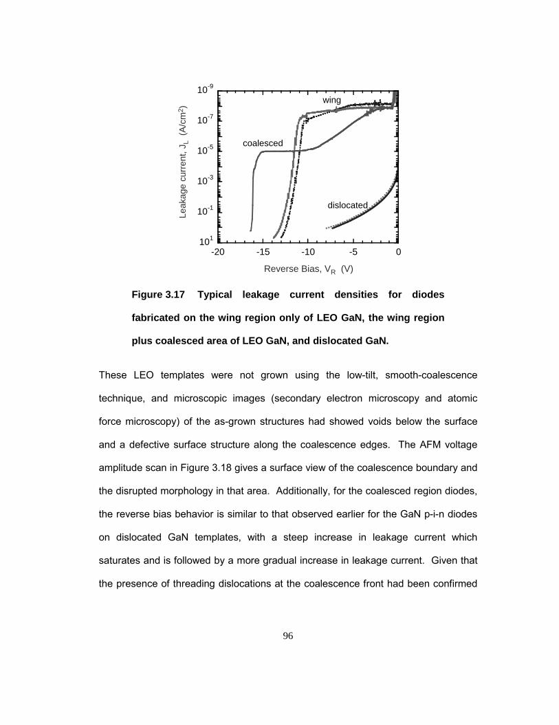
96
10-9
10-7
10-5
10-3
10-1
101
-20 -15 -10 -5 0
wing
coalesced
dislocated
Leak
age
curr
ent,
J L (
A/c
m2 )
Reverse Bias, VR (V)
Figure 3.17 Typical leakage current densities for diodes
fabricated on the wing region only of LEO GaN, the wing region
plus coalesced area of LEO GaN, and dislocated GaN.
These LEO templates were not grown using the low-tilt, smooth-coalescence
technique, and microscopic images (secondary electron microscopy and atomic
force microscopy) of the as-grown structures had showed voids below the surface
and a defective surface structure along the coalescence edges. The AFM voltage
amplitude scan in Figure 3.18 gives a surface view of the coalescence boundary and
the disrupted morphology in that area. Additionally, for the coalesced region diodes,
the reverse bias behavior is similar to that observed earlier for the GaN p-i-n diodes
on dislocated GaN templates, with a steep increase in leakage current which
saturates and is followed by a more gradual increase in leakage current. Given that
the presence of threading dislocations at the coalescence front had been confirmed

97
with AFM images, this is obviously the same mechanism as before, with leakage
current due to generation from or via traps.
Figure 3.18 AFM (voltage amplitude) image along coalescence
boundary of LEO GaN. Greyscale =0.5 V.
The current density of the diodes fabricated on the dislocated GaN was over six
orders of magnitude higher again, at 300 mA/cm2. For all of the diodes on the
dislocated wafer, in fact, the forward characteristics also showed heavy leakage.
This, coupled with the soft breakdown in reverse bias, attests to the presence of a
large leakage path. These diodes had much worse leakage than the GaN p-i-n
diodes on the dislocated template observed earlier in this chapter, resulting in a
much more dramatic contrast for leakage current with and without threading
dislocations. While this severe leakage path may be due to the dislocation-induced
enhanced defect formation in AlGaN seen in Chapter 2, it is more likely that, as
discussed earlier, it was processing-related.

98
3.4.4 Spectral response and threading dislocations
The responsivity curves further emphasize the effect of the dislocation structure on
the performance of the photodiodes. The best spectral response curves for the
different diodes are plotted in Figure 3.19.
10-5
10-4
10-3
10-2
10-1
200 250 300 350 400
wingcoalesceddislocated
Wavelength, λ (nm)
Res
pons
ivity
, R (
A/W
)
Figure 3.19 Spectral response curves for diodes fabricated on
the wing region only of LEO GaN, the wing region plus coalesced
area of LEO GaN, and dislocated GaN
The responses for the diodes fabricated on the LEO GaN (both wing-only and
coalesced) rise almost linearly with wavelength prior to the peak. The peak
responsivities are 0.050 A/W at 286 nm, and 0.047 A/W at 285 nm, for the wing-only
and coalesced-region diodes, respectively. (The slight variations in absolute value of
responsivity are due to thickness variations across the wafer area.) The

99
responsivities then drop three orders of magnitude over 26 nm and 30 nm,
respectively. Beyond that the photocurrent levels were below the detection limits of
the experimental setup.
Although the peak responsivity of the diode on the dislocated GaN (0.057 A/W at
287 nm) is comparable to that of the LEO-diodes, the curve itself is significantly
different. Firstly, the cutoff is broader � the responsivity takes 54 nm to drop by three
orders of magnitude after the peak. Again this can be explained by drawing on the
higher dislocation density in these diodes. Beyond the peak wavelength, the incident
UV light is not absorbed in the active region, however it will still be absorbed in the
p- and n-GaN layers due to the lower bandgap energy. At long wavelengths and due
to the thinness of the p-GaN this will mostly occur in the n-GaN below the active
region. Recalling the diode structure in Figure 3.15, the generated holes should not
contribute to the photocurrent if the valence band discontinuity and quantum wells
between the n-InGaN and the Al.33Ga.67N prevent their reaching the high-field region.
However for the dislocated GaN, leakage paths through to the depletion region result
in photocurrent from these minority holes generated below. This emerges as a
significant spectral response for wavelengths above cutoff. This leakage may result
from hopping conduction between localized traps associated with the dislocations.
Alternatively, the local perturbations in charge around threading dislocations,
particularly at the interface, may result in deformation of the band structure, thus
lowering the potential barrier and allowing the carriers to reach the depletion region.
The second difference in the spectral response is that the responsivity for
wavelengths below 250 nm is higher for diodes on the dislocated wafer. At these
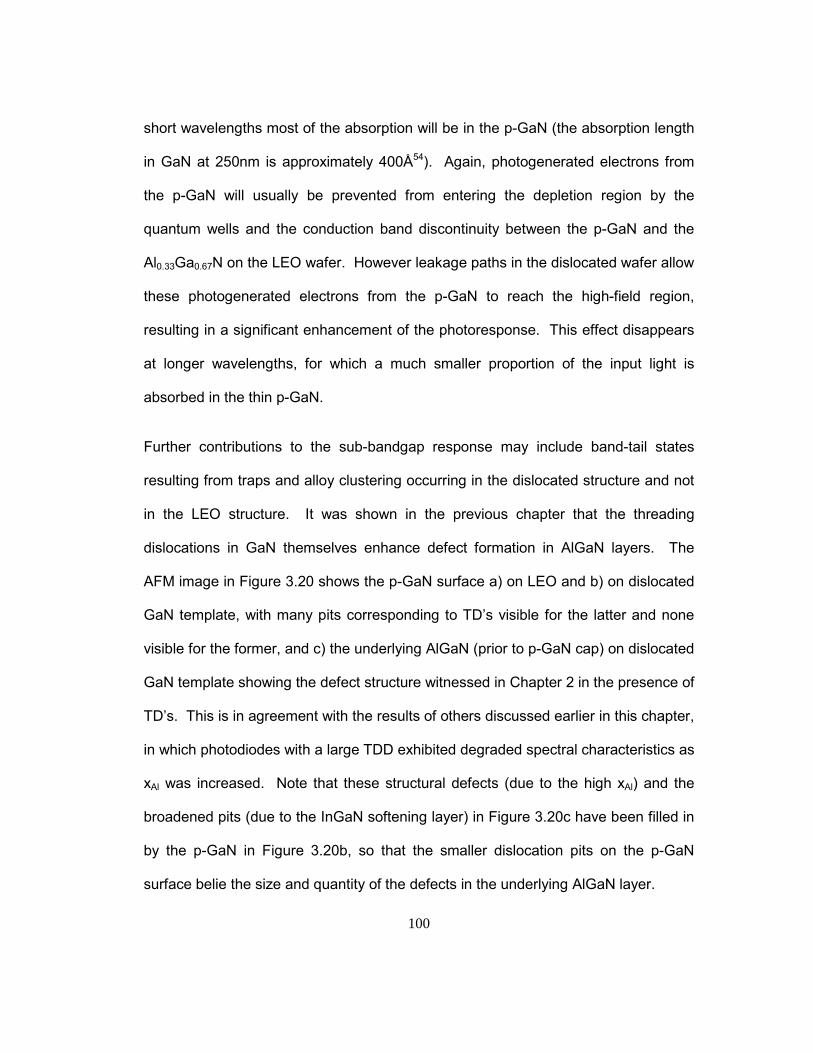
100
short wavelengths most of the absorption will be in the p-GaN (the absorption length
in GaN at 250nm is approximately 400Å54). Again, photogenerated electrons from
the p-GaN will usually be prevented from entering the depletion region by the
quantum wells and the conduction band discontinuity between the p-GaN and the
Al0.33Ga0.67N on the LEO wafer. However leakage paths in the dislocated wafer allow
these photogenerated electrons from the p-GaN to reach the high-field region,
resulting in a significant enhancement of the photoresponse. This effect disappears
at longer wavelengths, for which a much smaller proportion of the input light is
absorbed in the thin p-GaN.
Further contributions to the sub-bandgap response may include band-tail states
resulting from traps and alloy clustering occurring in the dislocated structure and not
in the LEO structure. It was shown in the previous chapter that the threading
dislocations in GaN themselves enhance defect formation in AlGaN layers. The
AFM image in Figure 3.20 shows the p-GaN surface a) on LEO and b) on dislocated
GaN template, with many pits corresponding to TD�s visible for the latter and none
visible for the former, and c) the underlying AlGaN (prior to p-GaN cap) on dislocated
GaN template showing the defect structure witnessed in Chapter 2 in the presence of
TD�s. This is in agreement with the results of others discussed earlier in this chapter,
in which photodiodes with a large TDD exhibited degraded spectral characteristics as
xAl was increased. Note that these structural defects (due to the high xAl) and the
broadened pits (due to the InGaN softening layer) in Figure 3.20c have been filled in
by the p-GaN in Figure 3.20b, so that the smaller dislocation pits on the p-GaN
surface belie the size and quantity of the defects in the underlying AlGaN layer.
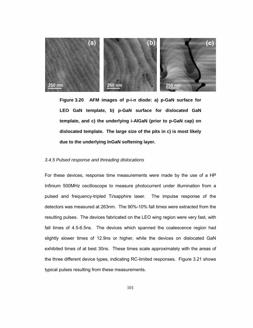
101
(a) (b) (c)
250 nm250 nm 250 nm
Figure 3.20 AFM images of p-i-n diode: a) p-GaN surface for
LEO GaN template, b) p-GaN surface for dislocated GaN
template, and c) the underlying i-AlGaN (prior to p-GaN cap) on
dislocated template. The large size of the pits in c) is most likely
due to the underlying InGaN softening layer.
3.4.5 Pulsed response and threading dislocations
For these devices, response time measurements were made by the use of a HP
Infinium 500MHz oscilloscope to measure photocurrent under illumination from a
pulsed and frequency-tripled Ti/sapphire laser. The impulse response of the
detectors was measured at 263nm. The 90%-10% fall times were extracted from the
resulting pulses. The devices fabricated on the LEO wing region were very fast, with
fall times of 4.5-6.5ns. The devices which spanned the coalescence region had
slightly slower times of 12.9ns or higher, while the devices on dislocated GaN
exhibited times of at best 30ns. These times scale approximately with the areas of
the three different device types, indicating RC-limited responses. Figure 3.21 shows
typical pulses resulting from these measurements.
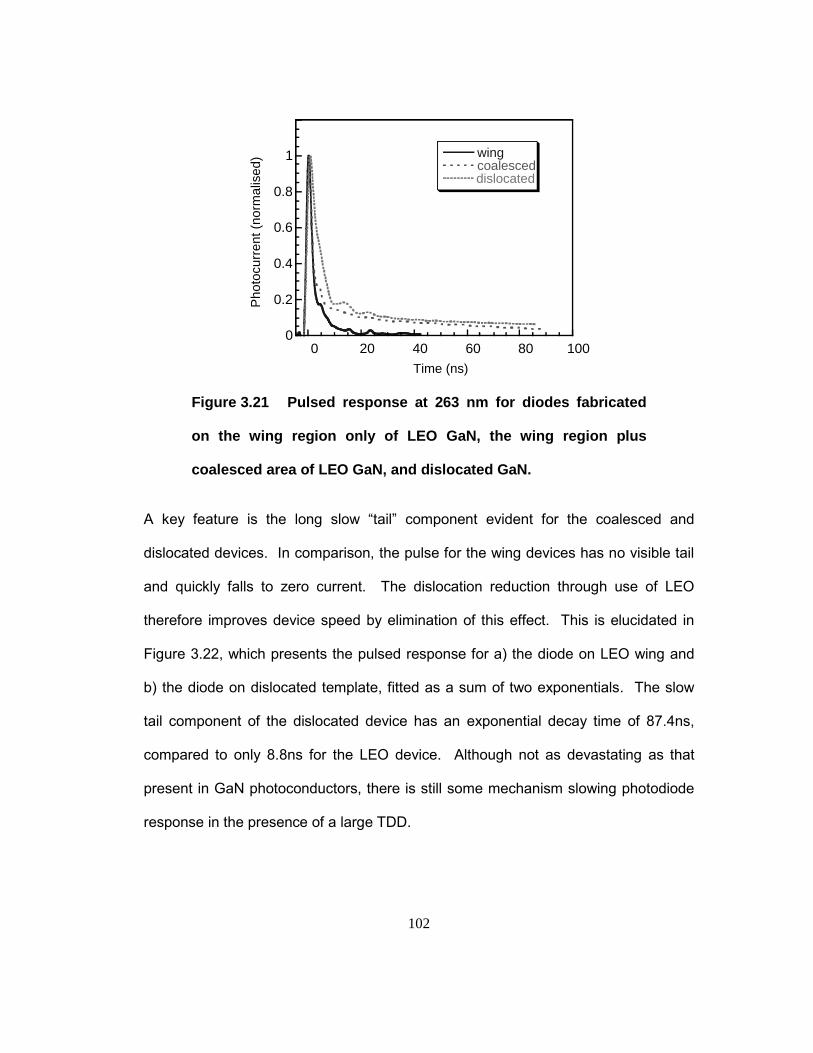
102
0
0.2
0.4
0.6
0.8
1
0 20 40 60 80 100
wingcoalesceddislocated
Pho
tocu
rren
t (no
rmal
ised
)
Time (ns)
Figure 3.21 Pulsed response at 263 nm for diodes fabricated
on the wing region only of LEO GaN, the wing region plus
coalesced area of LEO GaN, and dislocated GaN.
A key feature is the long slow �tail� component evident for the coalesced and
dislocated devices. In comparison, the pulse for the wing devices has no visible tail
and quickly falls to zero current. The dislocation reduction through use of LEO
therefore improves device speed by elimination of this effect. This is elucidated in
Figure 3.22, which presents the pulsed response for a) the diode on LEO wing and
b) the diode on dislocated template, fitted as a sum of two exponentials. The slow
tail component of the dislocated device has an exponential decay time of 87.4ns,
compared to only 8.8ns for the LEO device. Although not as devastating as that
present in GaN photoconductors, there is still some mechanism slowing photodiode
response in the presence of a large TDD.
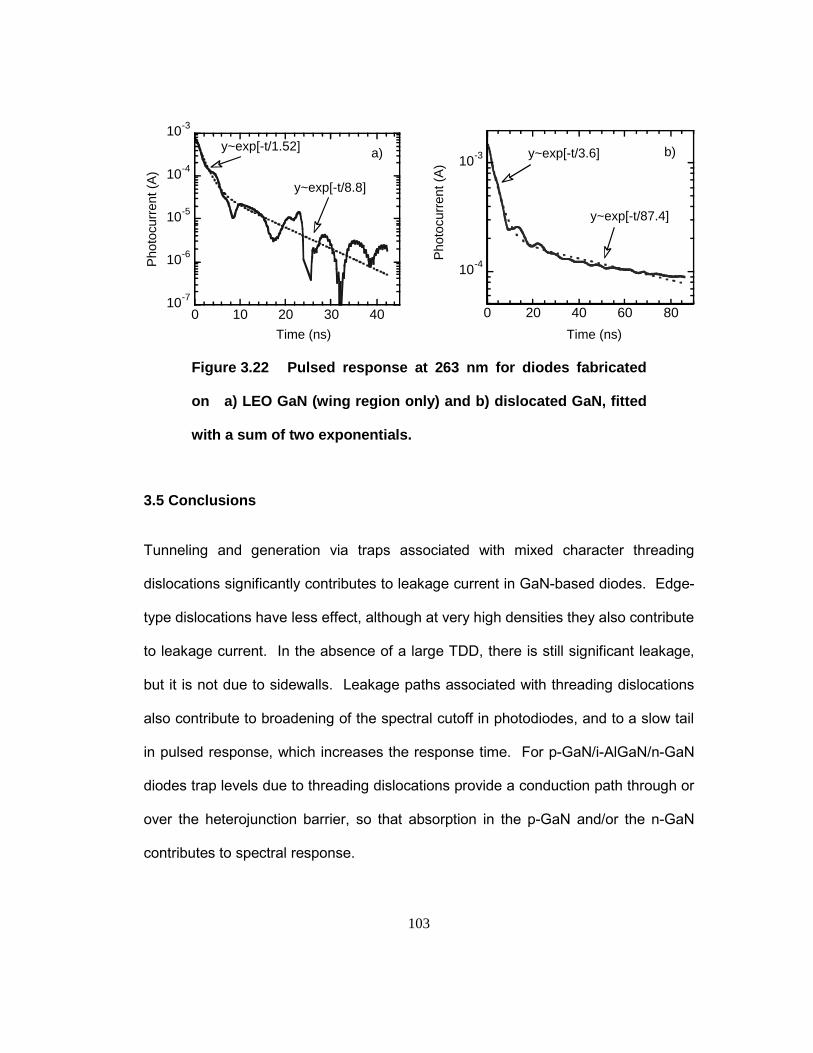
103
10-7
10-6
10-5
10-4
10-3
0 10 20 30 40
Pho
tocu
rren
t (A
)
Time (ns)
y~exp[-t/1.52]
y~exp[-t/8.8]
a)
Pho
tocu
rren
t (A
)
Time (ns)
10-4
10-3
0 20 40 60 80
y~exp[-t/3.6]
y~exp[-t/87.4]
b)
Figure 3.22 Pulsed response at 263 nm for diodes fabricated
on a) LEO GaN (wing region only) and b) dislocated GaN, fitted
with a sum of two exponentials.
3.5 Conclusions
Tunneling and generation via traps associated with mixed character threading
dislocations significantly contributes to leakage current in GaN-based diodes. Edge-
type dislocations have less effect, although at very high densities they also contribute
to leakage current. In the absence of a large TDD, there is still significant leakage,
but it is not due to sidewalls. Leakage paths associated with threading dislocations
also contribute to broadening of the spectral cutoff in photodiodes, and to a slow tail
in pulsed response, which increases the response time. For p-GaN/i-AlGaN/n-GaN
diodes trap levels due to threading dislocations provide a conduction path through or
over the heterojunction barrier, so that absorption in the p-GaN and/or the n-GaN
contributes to spectral response.
104
3.6 References
1. D. Hull. Introduction to Dislocations (1965), Pergamon Press, Oxford
2. H. Amano, N. Sawaki, I. Akasaki, and Y. Toyoda, �Metalorganic vapor phase epitaxial
growth of a high quality GaN film using an AlN buffer layer.� Appl. Phys. Lett. 48, 353-355
(1986).
3. B.P. Keller, S. Keller, D. Kapolnek, W.-N. Jiang, Y.-F. Wu, H. Masui, X.H. Wu, B.
Heying, J.S. Speck, U.K. Mishra, and S.P. DenBaars, �Metalorganic chemical vapor
deposition growth of high optical quality and high mobility GaN.� J. Electron. Mater. 24, 1707-
1709 (1995).
4. S. Keller, D. Kapolnek, B.P. Keller, Y.-F. Wu, B. Heying, J.S. Speck, U.K. Mishra, and
S.P. DenBaars, �Effect of the trimethylgallium flow during nucleation layer growth on the
properties of GaN grown on sapphire.� Jpn. J. Appl. Phys. 35, L285-288 (1996).
5. X.H. Wu, P. Fini, E.J. Tarsa, B. Heying, S. Keller, U.K. Mishra, S.P. DenBaars, and
J.S. Speck, �Dislocation generation in GaN heteroepitaxy.� J. Cryst. Growth 189/190, 231-
243 (1998).
6. K. Dovidenko, S. Oktyabrsky, J. Narayan, V. Joshkin and M. Razeghi, �Comparative
study of typical defects in III-nitride thin films and their alloys.� Mat. Res. Soc. Symp. Proc.
482, 411-416 (1998).
7. T. Hashimoto, M. Yuri, M. Ishida, Y. Terakoshi, O. Imafuji, T. Sugino, and K. Itoh,
�Reduction of threading dislocation in GaN on sapphire by buffer layer annealing in low-
pressure metalorganic chemical vapor deposition.� Jpn. J. Appl. Phys. 38, 6605-6610 (1996).
8. H. Lahrèche, M. Leroux, M. Laügt, M. Vaille, B. Beaumont, and P. Gibart, �Buffer free
growth of GaN on 6H-SiC by metalorganic vapor phase epitaxy.� J. Appl.Phys. 87, 577-583
(2000).

105
9. P. Waltereit, O. Brandt, A. Trampert, M. Ramsteiner, M. Reiche, M. Qi, and K.H.
Ploog, �Influence of AlN nucleation layers on growth mode and strain relief of GaN grown on
6H-SiC(0001).� Appl. Phys. Lett. 74, 3660-3662 (1999).
10. M.D. Bremser, W.G. Perry, T. Zhevela, N.V. Edwards, O.H. Nam, N. Parikh, D.E.
Aspnes, and Robert F. Davis, �Growth, doping and characterization of AlxGa1-xN thin film
alloys on 6H-SiC(0001) substrates.� MRS Internet J. Nitride Semicond. Res. 1, 8 (1996).
11. A. Kuramato (Fujitsu Laboratories), �Blue lasers on SiC substrate.�, UCSB Seminar,
Santa Barbara December 2000.
12. P. J. Hansen, Y.E. Strausser, A.N. Erickson, E.J. Tarsa, P. Kozodoy, E.G. Brazel,
J.P. Ibbetson, U. Mishra, V. Narayanamurti, S.P. DenBaars, and J.S. Speck, �Scanning
capacitance microscopy imaging of threading dislocations in GaN films grown on (0001)
sapphire by metalorganic chemical vapor deposition.� Appl. Phys. Lett. 72, 2247-2249
(1998).
13. E.G. Brazel, M.A. Chin, and V. Narayanamurti, �Direct observation of localized high
current densities in GaN films.� Appl. Phys. Lett. 74, 2367-2369 (1999).
14. A.E. Wickenden, D.D. Koleske, R.L. Henry, R.J. Gorman, M.E. Twigg, M. Fatemi,
J.A. Freitas Jr., and W.J. Moore, �The influence of OMVPE Growth Pressure on the
morphology, Compensation and Doping of GaN and Related Alloys.� J. Electron. Mater.29, 21-26 (2000).
15. C. Shi, P.M. Asbeck, and E.T. Yu, �Piezoelectric polarization associated with
dislocations in wurtzite GaN.� Appl. Phys. Lett. 74, 573-575 (1999).
16. S. Haffouz, H. Lahrèche, P. Vennéguès, P. de Mierry, B. Beaumont, F. Omnès, and
P. Gibart, �The effect of the Si/N treatment of a nitridated sapphire surface on the growth
mode of GaN in low-pressure metalorganic vapor phase epitaxy.� Appl. Phys. Lett. 73, 1278-
1280 (1998).
106
17. H. Lahrèche P. Vennéguès, B. Beaumont, and P. Gibart, �Growth of high-quality GaN
by low-pressure metal-organic vapour phase epitaxy (LP-MOVPE) from 3D islands and
lateral overgrowth.� J. Cryst. Growth 205, 245-252 (1999).
18. T. Wang, Y. Morishima, N. Naoi, and S. Sakai, �A new method for a great reduction
of dislocation density in GaN layer grown on a sapphire substrate.� J. Cryst. Growth 213, 188-192 (2000).
19. S. Tanaka, M. Takeuchi, and Y. Aoyagi, �Anti-surfactant in III-nitride epitaxy �
quantum dot formation and dislocation termination-.� Jpn. J. Appl. Phys. 39, 831-834 (2000).
20. S. Keller, G. Parish, J.S. Speck, S.P. DenBaars and U.K. Mishra, "Dislocation
reduction in GaN films through selective island growth of InGaN." Appl. Phys. Lett., 77(17),
2665-7 (2000). J. Appl. Phys 87(8) 3900-4 (2000)
21. H. Amano, M. Iwaya, N. Hayashi, T. Kashima, S. Nitta, C. Wetzel, and I. Akasaki,
�Control of dislocations and stress in AlGaN on sapphire using a low temperature interlayer.�
Phys. Stat. Sol. (b) 216, 683-689 (1999).
22. P. Kung, A. Saxler, D. Walker, X. Zhang, R. Lavado, K.S. Kim, and M. Razeghi
�AlxGa1-xN Based Materials and Heterostructures.� Mat. Res. Soc. Symp. Proc. 449, 79-84
(1997).
23. W.V Lundin, A.S. Usikov, B.V. Pushnyi, U.I. Ushakov, M.V. Stepanov, N.M. Shmidt,
T.V. Shubina, A.V. Sakharov, N.N. Faleev, V.A. Solov�ev, A.A. Sitnikova, Yu.A. Kudriavtsev,
B.Ya. Ber, and Y.M Zadiranov, �Optical and structural studies of thick AlGaN alloy layers and
AlGaN/GaN heterostructures on sapphire substrates.� Mat. Sci. Forum 264-268, 1315-1318
(1998).
24. H. Marchand, X.H. Wu, J.P. Ibbetson, P.T. Fini, P. Kozodoy, S. Keller, J.S. Speck,
S.P. DenBaars, and U.K. Mishra �Microstructure of GaN laterally overgrown by metalorganic
chemical vapor deposition.�Appl. Phys. Lett. 73, 747 (1998).
107
25. T.S. Zheleva, O.-H. Nam, M.D. Bremser, and R.F. Davis, �Dislocation density
reduction via lateral epitaxy in selectively grown GaN structures.� Appl. Phys. Lett. 71, 2472-
2474 (1997).
26. D. Kapolnek, S. Keller, R. Ventury, R.D. Underwood, P. Kozodoy, S.P. DenBaars,
and U.K. Mishra �Anisotropic epitaxial lateral growth in GaN selective area epitaxy.� Appl.
Phys. Lett. 71, 1204-1206 (1997).
27. O.-H. Nam, M.D. Bremser, T.S. Zheleva, and R.F. Davis �Lateral epitaxy of low
defect density GaN layers via organometallic vapor phase epitaxy.� Appl. Phys. Lett. 71, 2638-2640 (1997).
28. M.E. Coltrin, C.C. Willan, M.E. Bartram, J. Han, N. Missert, M.H. Crawford, and A.G.
Baca ,�Transport, growth mechanisms, and material quality in GaN epitaxial lateral
overgrowth.� MRS Internet J. Nitride Semicond. Res. 4S1, G6.9 (1999).
29. F. Binet, J.Y. Duboz, E. Rosencher, F. Scholz, and V. Hãrle, �Mechanisms of
recombination in GaN photodetectors.� Appl. Phys. Lett. 69, 1202-1204 (1996).
30. Z.C. Huang, D.B. Mott, P.K. Shu, R. Zhang, J.C. Chen, and D.K. Wickenden �Optical
quenching of photoconductivity in GaN photoconductors.� J. Appl. Phys. 82, 2707-2709
(1997).
31. E. Monroy, J.A. Garrido, E. Muñoz, I. Izpura, F.J. Sánchez, M.A. Sánchez-García, E.
Calleja, B. Beaumont, and Pierre Gibart, �Characterization and modelling of photoconductive
GaN ultraviolet detectors.� MRS Internet J. Nitride Semicond. Res. 2, Article 12 (1997).
32. Z.C. Huang, D.B. Mott, P.K. Shu, J.C. Chen, and D.K. Wickenden, �Improvement of
metal-semiconductor-metal GaN photoconductors.� J. Electron. Mater. 26, 330-333 (1997).
33. G.M. Smith, J.M. Redwing, R.P. Vaudo, E.M. Ross, J.S. Flynn, and V.M. Phanse,
�Substrate effects on GaN photoconductive detector performance.� Appl. Phys. Lett. 75, 25-
27 (1999).
108
34. J.T. Torvik, J.I. Pankove, S. Nakamura, I. Grzegory, and S. Porowski �The effect of
threading dislocations, Mg doping, and etching on the spectral responsitivity in GaN-based
ultraviolet detectors.� J. Appl. Phys. 86, 4588-4593 (1999).
35. P. Kozodoy, J.P. Ibbetson, H. Marchand, P.T. Fini, S. Keller, J.S. Speck, S.P.
DenBaars, and U.K. Mishra, �Electrical characterization of GaN p-n junctions with and without
threading dislocations.� Appl. Phys. Lett. 73, 975-977 (1998).
36. G. Parish, S. Keller, P. Kozodoy, J. P. Ibbetson, H. Marchand, P. T. Fini, S.B.
Fleischer, S. P. DenBaars, U. K. Mishra and E.J. Tarsa, �High-performance (Al,Ga)N-based
solar-blind ultraviolet p-i-n detectors on laterally epitaxially overgrown GaN� Appl. Phys. Lett.
75(2), 247-9 (1999).
37. E. Monroy, F. Calle, E. Muñoz, B. Beaumont, F. Omnès, and P. Gibart �Schottky
barrier ultraviolet photodetectors on epitaxial lateral overgrown GaN.� Phys. Stat. Sol. (a)
176, 141-145 .(1999).
38. P. Sandvik, D. Walker, P. Kung, K. Mi, F. Shahedipour, V. Kumar, X. Zhang, J. Diaz,
C. Jelen, and M. Razeghi �Solar-blind AlxGa1-xN p-i-n photodetectors grown on LEO and non-
LEO GaN.� Proc. SPIE 3948, 265-272 (2000).
39. A. Osinsky, S. Gangopadhyay, R. Gaska, B. Williams, M.A. Khan, D. Kuksenkov, and
H. Temkin, �Low noise p-π-n ultraviolet photodetectors.� Appl. Phys. Lett. 71, 2334-2336
(1997).
40. C. Pernot, A. Hirano, M. Iwaya, T. Detchprohm, H. Amano, and I. Akasaki
�Improvement of low-intensity ultraviolet photodetectors based on AlGaN with low threading
dislocation density.� Phys. Stat. Sol. (a) 176, 147-151 (1999).
41. C. Pernot, A. Hirano, M. Iwaya, T. Detchprohm, H. Amano, and I. Akasaki, �Solar-
Blind UV photodetectors based on GaN/AlGaN p-i-n photodiodes.� Jpn. J. Appl. Phys. 39, 387-389 (2000).
42. E. Monroy, M. Hamilton, D. Walker, P. Kung, F.J. Sánchez, and M. Razeghi, �High-
quality visible-blind AlGaN p-i-n photodiodes.�Appl. Phys. Lett. 74, 1171-1173 (1999).
109
43. E. Monroy, F. Calle, J.L. Paul, F.J. Sánchez, E. Muñoz, F. Omnès, B. Beaumont, and
P. Gibart �Analysis and modeling of AlxGa1-xN-based Schottky barrier photodiodes.�J. Appl.
Phys. 88, 2081-2091 (2000).
44. K.L. Ashley and A.G. Milnes, �Double injection in deep-lying impurity semiconductors�
J. Appl. Phys. 35, 369-374 (1964).
45. S.M. Sze, Physics of Semiconductor Devices (1981) John Wiley & Sons, New York.
46. B. Heying, X.H. Wu, S. Keller, Y. Li, D. Kapolnek, B.P. Keller, S.P. DenBaars, and
J.S. Speck, �Role of threading dislocation structure on the X-ray diffraction peak widths in
epitaxial GaN films.� Appl. Phys. Lett. 68, 643-645 (1996).
47. V. Srikant, J. Speck, and D. Clarke, �Mosaic structure in epitaxial films having large
lattice mismatch.� J. Appl. Phys. 82, 4286-4295 (1997).
48. S. Keller, U.K. Mishra, S.P. DenBaars, and W. Seifert, �Spiral growth of InGaN
nanoscale islands on GaN.� Jpn. J. Appl. Phys. 37, L431-434 (1998).
49. D.V. Kuksenkov, H. Temkin, A. Osinsky, R. Gaska, and M.A. Khan �Origin of
conductivity and low-frequency noise in reverse-biased GaN p-n junction.� Appl. Phys. Lett.
72, 1365-1367 (1998).
50. A.V. Sampath, E. Iliopoulos, K. Seth, Y. Fedyunin, M. Misra, H.M. Ng, P. Lamarre, Z.
Feit, and T.D. Moustakas �GaN photodiodes grown by MBE on HVPE and ELO-HVPE
GaN\sapphire substrates.� Proc. SPIE 3948, 311-318 (2000).
51. P. Fini, L. Zhao, B. Moran, M. Hansen, H. Marchand, J.P. Ibbertson, S.P. DenBaars,
U.K. Mishra, and J.S. Speck �High-quality coalescence of laterally overgrown GaN/sapphire
seed layers.� Appl. Phys. Lett. 75, 1706-1708 (1999).
52. E. J. Tarsa, P. Kozodoy, J. Ibbetson, B. P. Keller, G. Parish, and U.K. Mishra �Solar-
blind AlGaN-based inverted heterostructure photodiodes.� Appl. Phys. Lett. 77, 316-318
(2000).
110
53. D.L. Pulfrey, J.J. Kuek, M.P. Leslie, B.D. Nener, G. Parish, U.K. Mishra, P. Kozodoy
and E.J. Tarsa, "High UV/solar rejection ratios in GaN/AlGaN/GaN p-i-n photodiodes." IEEE
Trans. on Electron Device. 48(3), 100-102 (2001).
54. G. Yu, G. Wang, H. Ishikawa, M. Umeno, T. Soga, T. Egawa, J. Watanabe, and T.
Jimbo, �Optical properties of wurtzite structure GaN on sapphire around ellipsometry and the
optical transmission method.� Appl. Phys. Lett. 70, 3209-3211 (1997).
111
Chapter 4. Thick AlGaN for solar-blind detectors
4.1 Developing a solar-blind p-i-n detector structure
The knowledge gained from the experiments detailed in Chapter 2 and Chapter 3
was combined to design and grow a solar-blind p-i-n detector structure.
4.1.1 Synopsis of this chapter
The study into the effects of dislocations on the p-GaN/i-AlGaN/n-GaN solar-blind
detector (Section 3.4) highlighted drawbacks in that particular structure. Firstly there
was the non-solar-blind response from the GaN, which broadened the cutoff,
particularly in the presence of dislocations. Secondly, the peak responsivity was
limited to only 0.05A/W because the thickness of the AlGaN could not be increased
without cracking. In this section, some further studies of this structure are presented,
along with investigations into dislocation reduction in bulk Al0.35Ga0.65N, utilizing LEO
techniques. Following that, Section 4.2 details the experiments into growth of thick
Al0.35Ga0.65N on SiC substrate. These experiments were undertaken in the hope that
the benefits to detector performance, as well as the possibility of avoiding costly and
time-consuming LEO, would outweigh the increase in substrate cost, when using SiC
substrate. The studies included investigations into the nucleation technique and into
the Al0.35Ga0.65N growth conditions and doping, as well as attempts to reduced the
high edge dislocation density by using SixNy interlayers. Finally the results for the
first solar-blind AlxGa1-xN detectors grown on SiC substrates are presented in Section
4.3, including a comparison of devices with and without a conducting buffer.
112
4.1.2 GaN absorption in GaN/AlGaN/GaN p-i-n
A simple experiment was devised to determine whether the source of the longer-
wavelength spectral response in the p-GaN/i-AlGaN/n-GaN photodiode was
absorption in the p-GaN or in the n-GaN. Figure 4.1 replicates the schematics given
in Figure 3.15, of the structure cross-section and schematic, along with an indication
of the modifications made for this experiment. Two modified structures were grown,
in which the GaN/AlGaN interface barrier was changed. Figure 4.1 illustrates the
first of these, in which the conduction band barrier to electrons at the p-GaN/
i-Al0.33Ga0.67N interface was enhanced. This was achieved by grading the AlGaN
composition to 0.5 over the last 50Å before the p-GaN. The second modified
structure (not shown) had an enhanced valence band barrier to holes at the
i- Al0.3Ga0.67N /n-InGaN interface, achieved by grading the AlGaN composition from
0.5 over the first 50Å after the n-InGaN (recall that a thin In0.04Ga0.96N softening layer
was used between the n-GaN and the AlGaN). Note that in this study the quantum
wells were not included, in order to assess the full effect of the interfacial barriers on
carrier transport.
Figure 4.2 compares the spectral response of typical devices for each of the two
modified structures. They are designated ∆EC and ∆EV, for the structures with
enhanced electron and hole barriers, respectively. Many devices were measured
from each of the two wafers, and the trends that are seen here were true for all
devices.
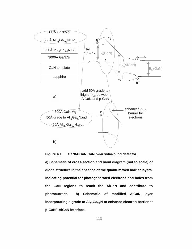
50Å
e-
EG(AlGaN)EG(GaN)
EG(GaN)hν
h+
sapphire
3000Å GaN:Si
250Å In.04Ga.96N:Si
500Å Al.33Ga.67N:uid
300Å GaN:Mg
GaN template
4
add 50A grade to higher xAl between
Figu
a) S
diod
indi
the
pho
inco
p-G
a)grade to Al.5Ga.5N:uid
50Å Al.33Ga.67N:uid
300Å GaN:Mg
AlGaN and p-GaN
enhanced ∆EC barrier for electrons
e-
b)113
re 4.1 GaN/AlGaN/GaN p-i-n solar-blind detector.
chematic of cross-section and band diagram (not to scale) of
e structure in the absence of the quantum well barrier layers,
cating potential for photogenerated electrons and holes from
GaN regions to reach the AlGaN and contribute to
tocurrent. b) Schematic of modified AlGaN layer
rporating a grade to Al0.5Ga0.5N to enhance electron barrier at
aN/i-AlGaN interface.
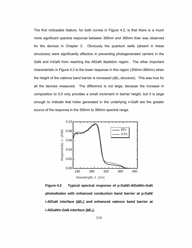
114
The first noticeable feature, for both curves in Figure 4.2, is that there is a much
more significant spectral response between 300nm and 360nm than was observed
for the devices in Chapter 3. Obviously the quantum wells (absent in these
structures) were significantly effective in preventing photogenerated carriers in the
GaN and InGaN from reaching the AlGaN depletion region. The other important
characteristic in Figure 4.2 is the lower response in this region (300nm-360nm) when
the height of the valence band barrier is increased (∆EV structure). This was true for
all the devices measured. The difference is not large, because the increase in
composition to 0.5 only provides a small increment in barrier height, but it is large
enough to indicate that holes generated in the underlying n-GaN are the greater
source of the response in the 300nm to 360nm spectral range.
0.00
0.02
0.04
0.06
0.08
0.10
240 280 320 360 400
∆Ev∆ Ec
Res
pons
ivity
, R (
A/W
)
Wavelength, λ (nm)
Figure 4.2 Typical spectral response of p-GaN/i-AlGaN/n-GaN
photodiodes with enhanced conduction band barrier at p-GaN/
i-AlGaN interface (∆∆∆∆EC) and enhanced valence band barrier at
i-AlGaN/n-GaN interface (∆∆∆∆EV).
115
To obtain higher responsivity, the requirements of thicker i-AlGaN necessitate growth
on an AlGaN template to avoid cracking. That is, the n-layer of the p-i-n should also
be AlGaN. Additionally, after now determining that the n-GaN was the main region
from which undesired spectral response was originating, it is evident that the use of
an n-AlGaN layer will improve the cutoff characteristics. However the p-GaN layer
can be retained so as to avoid the difficulties in acquiring p-Al0.35Ga0.65N.
4.1.3 Thicker AlGaN by LEO
The investigations in Chapter 3 revealed unequivocally that threading dislocations
are detrimental to multiple aspects of device performance. LEO had already proven
to be a successful technique for dislocation reduction in GaN. For AlGaN it presents
the additional incentive of reduced tension in the overgrown layer and therefore the
possibility of growing thick AlGaN layers on GaN templates.
Reports in the literature for Al0.1Ga0.9N had already indicated problems with
selectivity of the AlGaN using conventional SiO2 and Si3N4 mask materials, even at
low compositions1. Thus, several different mask materials were tested for
Al0.35Ga0.65N selectivity. Figure 4.3 presents optical photographs of four different
mask materials after regrowth, using a mask pattern with stripes oriented at 4°
increments. The four mask materials compared were a) SiO2, b) sapphire, c) Pt and
d) TiN. The sapphire �mask� was obtained by etching a GaN template down to the
sapphire substrate, in those areas in which SiO2 would have been deposited for a
conventional LEO mask. The TiN mask was obtained by annealing a Ti mask in N2
ambient. Parameters such as growth temperature, growth rate, and carrier gas were
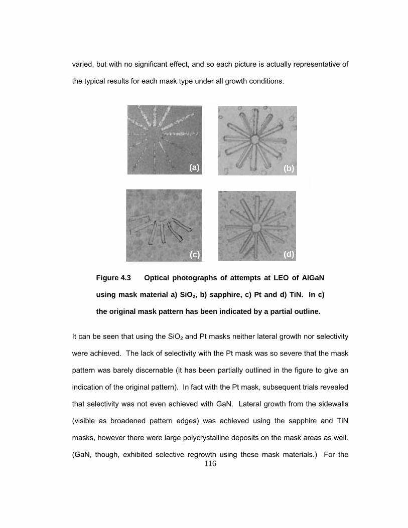
116
varied, but with no significant effect, and so each picture is actually representative of
the typical results for each mask type under all growth conditions.
(a) (b)
(c) (d)
Figure 4.3 Optical photographs of attempts at LEO of AlGaN
using mask material a) SiO2, b) sapphire, c) Pt and d) TiN. In c)
the original mask pattern has been indicated by a partial outline.
It can be seen that using the SiO2 and Pt masks neither lateral growth nor selectivity
were achieved. The lack of selectivity with the Pt mask was so severe that the mask
pattern was barely discernable (it has been partially outlined in the figure to give an
indication of the original pattern). In fact with the Pt mask, subsequent trials revealed
that selectivity was not even achieved with GaN. Lateral growth from the sidewalls
(visible as broadened pattern edges) was achieved using the sapphire and TiN
masks, however there were large polycrystalline deposits on the mask areas as well.
(GaN, though, exhibited selective regrowth using these mask materials.) For the
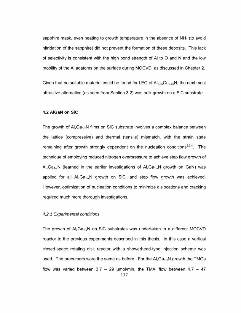
117
sapphire mask, even heating to growth temperature in the absence of NH3 (to avoid
nitridation of the sapphire) did not prevent the formation of these deposits. This lack
of selectivity is consistent with the high bond strength of Al to O and N and the low
mobility of the Al adatoms on the surface during MOCVD, as discussed in Chapter 2.
Given that no suitable material could be found for LEO of Al0.35Ga0.65N, the next most
attractive alternative (as seen from Section 3.2) was bulk growth on a SiC substrate.
4.2 AlGaN on SiC
The growth of AlxGa1-xN films on SiC substrate involves a complex balance between
the lattice (compressive) and thermal (tensile) mismatch, with the strain state
remaining after growth strongly dependent on the nucleation conditions2,3,4. The
technique of employing reduced nitrogen overpressure to achieve step flow growth of
AlxGa1-xN (learned in the earlier investigations of AlxGa1-xN growth on GaN) was
applied for all AlxGa1-xN growth on SiC, and step flow growth was achieved.
However, optimization of nucleation conditions to minimize dislocations and cracking
required much more thorough investigations.
4.2.1 Experimental conditions
The growth of AlxGa1-xN on SiC substrates was undertaken in a different MOCVD
reactor to the previous experiments described in this thesis. In this case a vertical
closed-space rotating disk reactor with a showerhead-type injection scheme was
used. The precursors were the same as before. For the AlxGa1-xN growth the TMGa
flow was varied between 3.7 � 29 µmol/min, the TMAl flow between 4.7 � 47

118
µmol/min, and the ammonia flow between 0.05 � 0.13 mol/min. Variations in growth
rate were achieved by changing the group III flows. The thermocouple temperature
ranged from 1090 to 1180°C. The thermocouple was situated underneath the SiC-
coated graphite susceptor, and the actual surface temperature was approximately
130°C below the thermocouple temperature. All temperatures quoted here will be
the thermocouple temperatures. The total gas flow was varied between 5 - 16 l/min,
and the reactor pressure was 100 Torr. The solid composition of the bulk AlxGa1-xN
was kept constant at 0.35, although it varied with growth conditions between
approximately 0.3-0.4.
4.2.2 Nucleation conditions
Three types of growth initiation were examined for the AlGaN growth on SiC. These
were direct, high-temperature growth; graded (from a higher composition of 0.5-0.6)
direct growth; and a lower temperature (1050°C) AlN nucleation layer. The graded
composition technique will be referred to as the graded buffer in the discussions in
this chapter. Schematics of these three types of structures are given in Figure 4.4.
Figure 4.5 displays AFM images for a typical 400nm Al0.4Ga0.6N layer on SiC (with a
graded buffer). The image areas are 1µm x 1µm, 5µm x 5µm, and 20µm x 20µm. In
the first, 1µm x 1µm image (Figure 4.5a), steps are visible, confirming that step-flow
growth mode was achieved. Also apparent in this image is the high density of dark
spots, which correspond to threading dislocations. Counting of the visible pits gives
a lower bound for the TDD of 4x1010cm-2 for this particular wafer. In the larger AFM
image areas (Figures 4.5b and 4.5c), islands of 1-5µm diameter are visible.
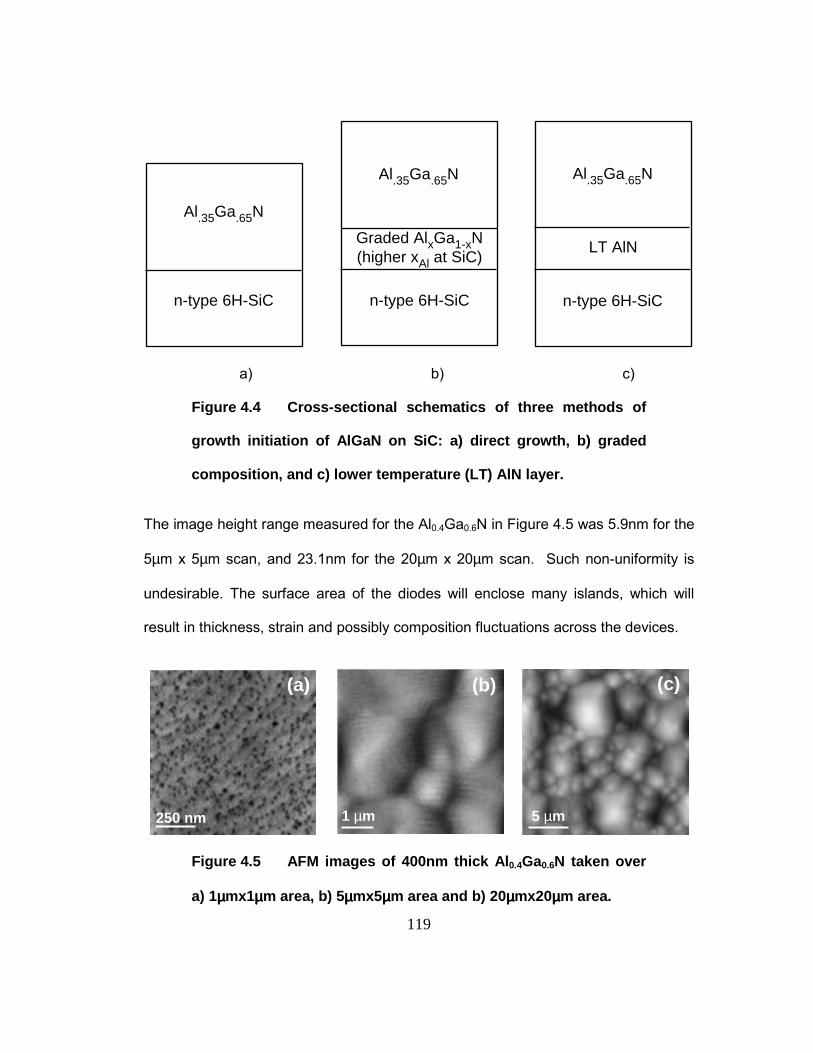
119
Al.35Ga.65N
n-type 6H-SiC n-type 6H-SiC n-type 6H-SiC
Al.35Ga.65N
Graded AlxGa1-xN(higher xAl at SiC)
Al.35Ga.65N
LT AlN
a) b) c)
Figure 4.4 Cross-sectional schematics of three methods of
growth initiation of AlGaN on SiC: a) direct growth, b) graded
composition, and c) lower temperature (LT) AlN layer.
The image height range measured for the Al0.4Ga0.6N in Figure 4.5 was 5.9nm for the
5µm x 5µm scan, and 23.1nm for the 20µm x 20µm scan. Such non-uniformity is
undesirable. The surface area of the diodes will enclose many islands, which will
result in thickness, strain and possibly composition fluctuations across the devices.
(b) (c)
1 µm 5 µm
(a)
250 nm
Figure 4.5 AFM images of 400nm thick Al0.4Ga0.6N taken over
a) 1µµµµmx1µµµµm area, b) 5µµµµmx5µµµµm area and b) 20µµµµmx20µµµµm area.
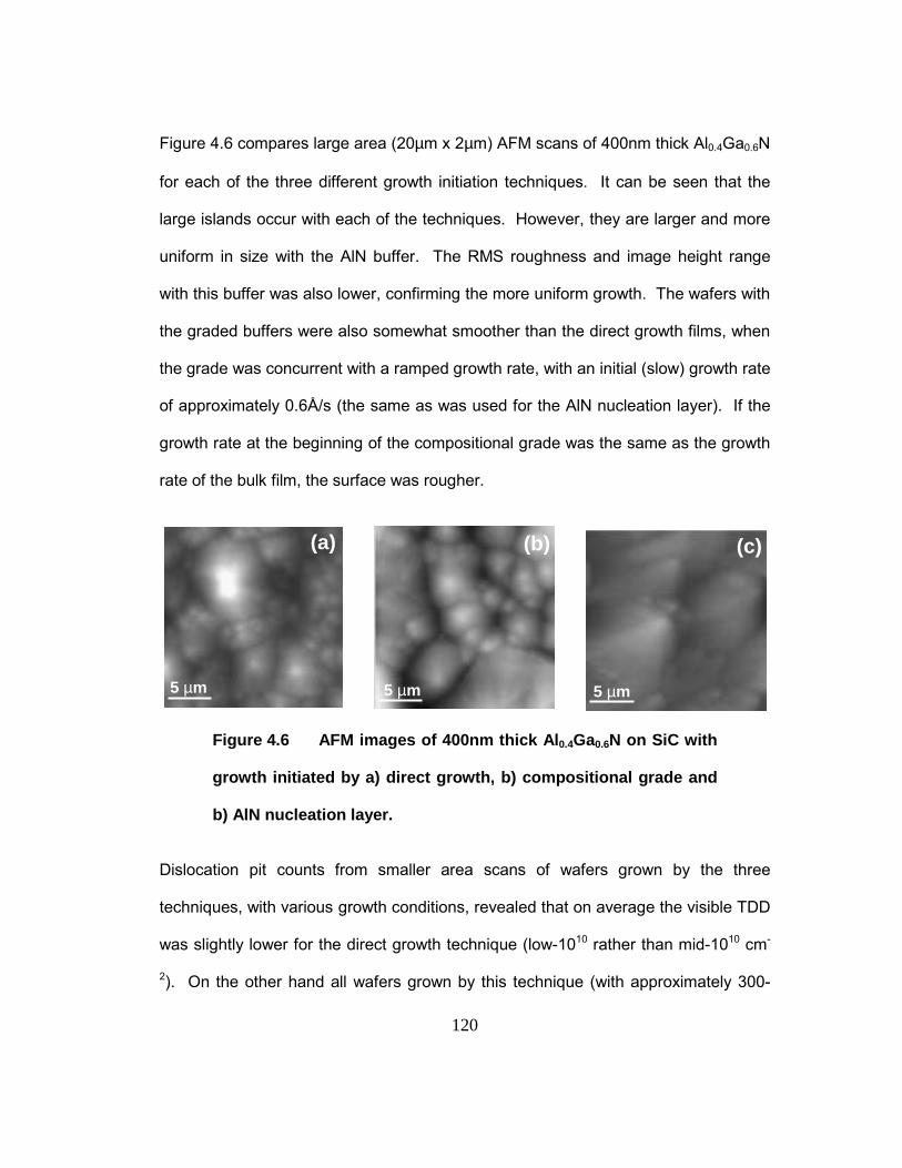
120
Figure 4.6 compares large area (20µm x 2µm) AFM scans of 400nm thick Al0.4Ga0.6N
for each of the three different growth initiation techniques. It can be seen that the
large islands occur with each of the techniques. However, they are larger and more
uniform in size with the AlN buffer. The RMS roughness and image height range
with this buffer was also lower, confirming the more uniform growth. The wafers with
the graded buffers were also somewhat smoother than the direct growth films, when
the grade was concurrent with a ramped growth rate, with an initial (slow) growth rate
of approximately 0.6Å/s (the same as was used for the AlN nucleation layer). If the
growth rate at the beginning of the compositional grade was the same as the growth
rate of the bulk film, the surface was rougher.
5 µm 5 µm 5 µm
(b) (c)(a)
Figure 4.6 AFM images of 400nm thick Al0.4Ga0.6N on SiC with
growth initiated by a) direct growth, b) compositional grade and
b) AlN nucleation layer.
Dislocation pit counts from smaller area scans of wafers grown by the three
techniques, with various growth conditions, revealed that on average the visible TDD
was slightly lower for the direct growth technique (low-1010 rather than mid-1010 cm-
2). On the other hand all wafers grown by this technique (with approximately 300-
121
400nm thickness of AlGaN) were cracked. The same was true for graded buffer
wafers without the ramp from slow growth rate. In contrast, the wafers with graded
buffer and ramped growth rate, and with AlN nucleation layer, were not cracked (for
a thickness of at least 450nm, the thickest films attempted). Initiating growth at a
lower growth rate, whether it be for an AlN nucleation layer or graded composition
buffer, results in less tensile strain in the post-growth film. This is consistent with the
studies of Waltereit et al.3, in which the lattice mismatch was relieved during growth
for direct growth of GaN on SiC, resulting in tensile strain in the final film, whereas
use of a coherently grown AlN nucleation layer resulted in a slightly compressive
strain in the GaN film. A coherently grown nucleation layer will not relieve lattice
mismatch. Obviously the nucleation layer must be grown at a low growth rate for
this. Variation of other growth conditions, notably temperature and total flow, did not
alleviate the cracking problem for the directly grown films.
Because of the cracking, the direct growth technique was not feasible for detector
structures. Instead the graded buffer and AlN buffer structures were used. In the
case of a conducting graded buffer, backside contacts can be used to avoid the need
for ohmic contacts to the resistive n-type AlGaN. However the distance between the
depletion region and the SiC substrate must be sufficient that no photo-generated
holes from the SiC will reach the depletion region. Otherwise there will be non-solar-
blind response as there was with the p-GaN/i-AlGaN/n-GaN structure (the bandgap
of SiC is 2.9eV, even narrower than GaN, although it is indirect and therefore less
efficient for photo-generation of carriers).
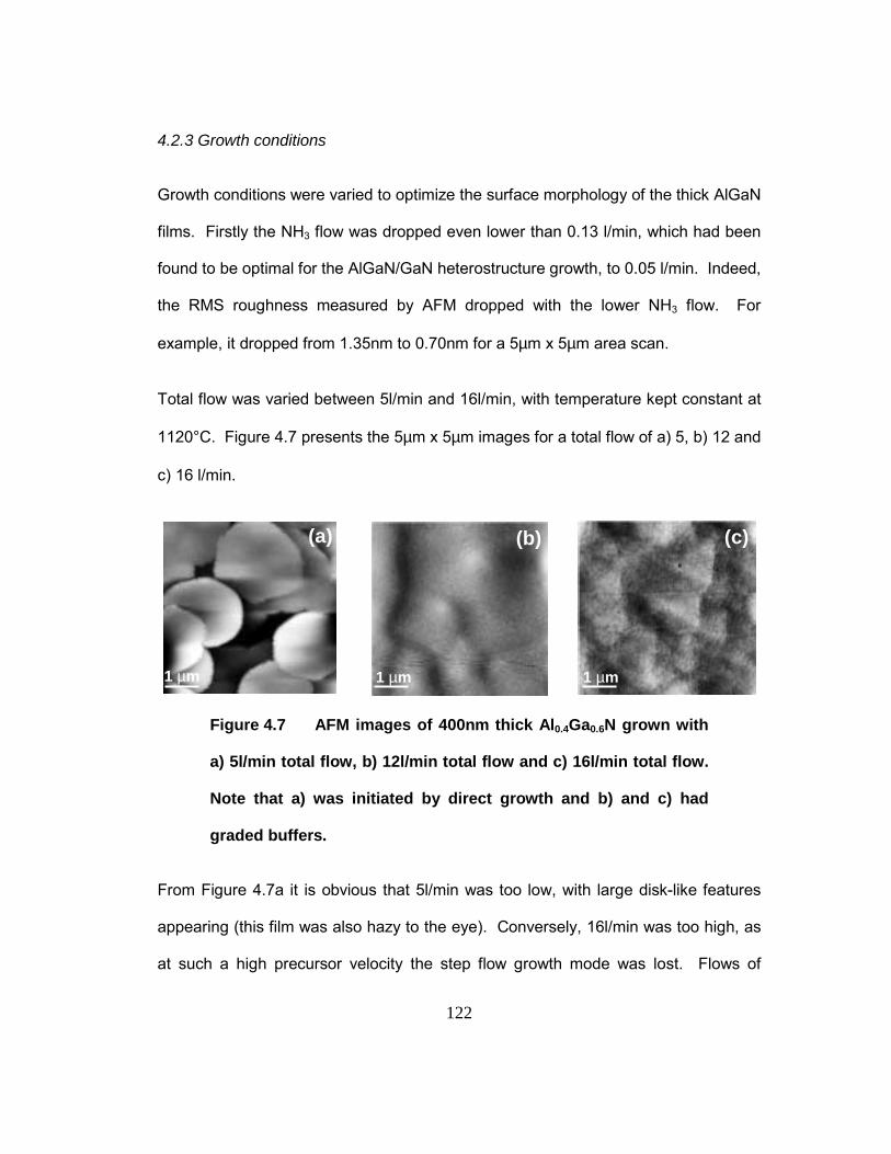
122
4.2.3 Growth conditions
Growth conditions were varied to optimize the surface morphology of the thick AlGaN
films. Firstly the NH3 flow was dropped even lower than 0.13 l/min, which had been
found to be optimal for the AlGaN/GaN heterostructure growth, to 0.05 l/min. Indeed,
the RMS roughness measured by AFM dropped with the lower NH3 flow. For
example, it dropped from 1.35nm to 0.70nm for a 5µm x 5µm area scan.
Total flow was varied between 5l/min and 16l/min, with temperature kept constant at
1120°C. Figure 4.7 presents the 5µm x 5µm images for a total flow of a) 5, b) 12 and
c) 16 l/min.
1 µm1 µm
(b)(a) (c)
1 µm
Figure 4.7 AFM images of 400nm thick Al0.4Ga0.6N grown with
a) 5l/min total flow, b) 12l/min total flow and c) 16l/min total flow.
Note that a) was initiated by direct growth and b) and c) had
graded buffers.
From Figure 4.7a it is obvious that 5l/min was too low, with large disk-like features
appearing (this film was also hazy to the eye). Conversely, 16l/min was too high, as
at such a high precursor velocity the step flow growth mode was lost. Flows of
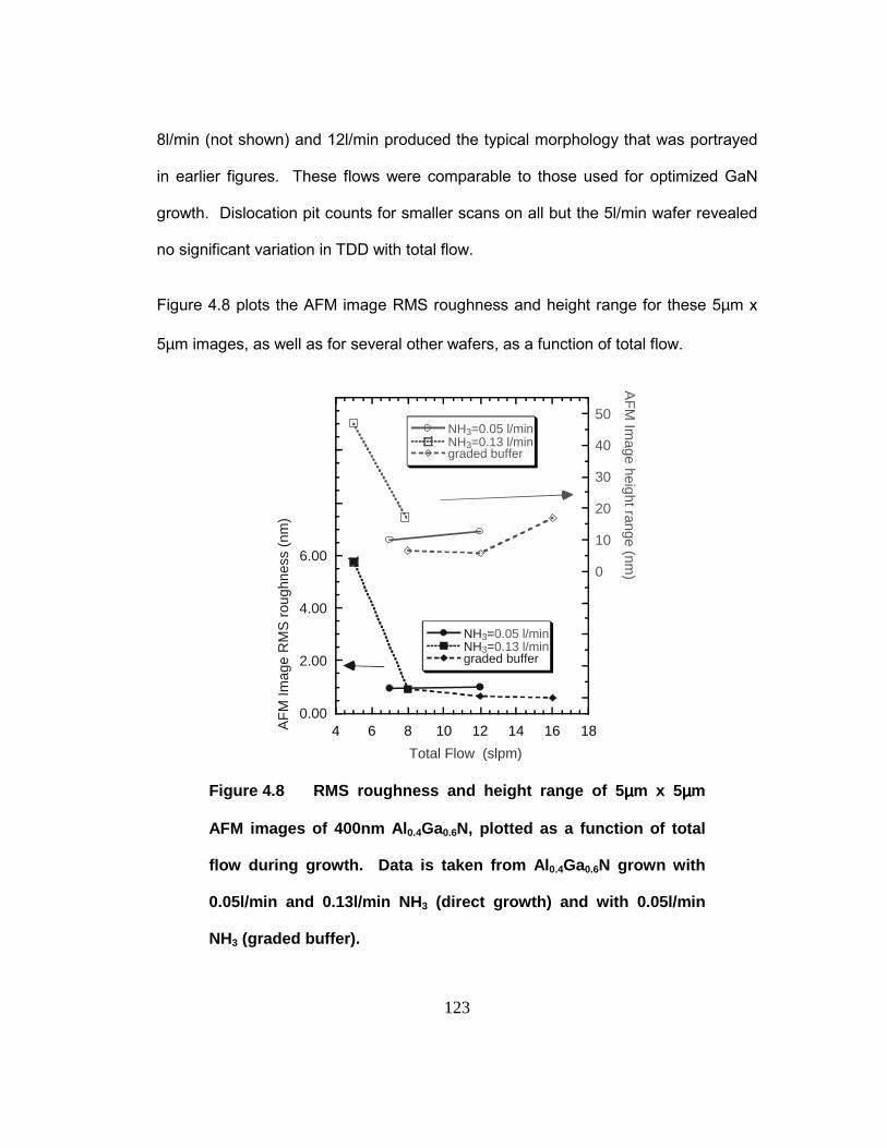
123
8l/min (not shown) and 12l/min produced the typical morphology that was portrayed
in earlier figures. These flows were comparable to those used for optimized GaN
growth. Dislocation pit counts for smaller scans on all but the 5l/min wafer revealed
no significant variation in TDD with total flow.
Figure 4.8 plots the AFM image RMS roughness and height range for these 5µm x
5µm images, as well as for several other wafers, as a function of total flow.
0.00
2.00
4.00
6.000
10
20
30
40
50
4 6 8 10 12 14 16 18
NH3=0.05 l/minNH3=0.13 l/mingraded buffer
NH3=0.05 l/minNH3=0.13 l/mingraded buffer
AF
M Im
age
RM
S r
ough
ness
(nm
)
AF
M Im
age height range (nm)
Total Flow (slpm)
Figure 4.8 RMS roughness and height range of 5µµµµm x 5µµµµm
AFM images of 400nm Al0.4Ga0.6N, plotted as a function of total
flow during growth. Data is taken from Al0.4Ga0.6N grown with
0.05l/min and 0.13l/min NH3 (direct growth) and with 0.05l/min
NH3 (graded buffer).
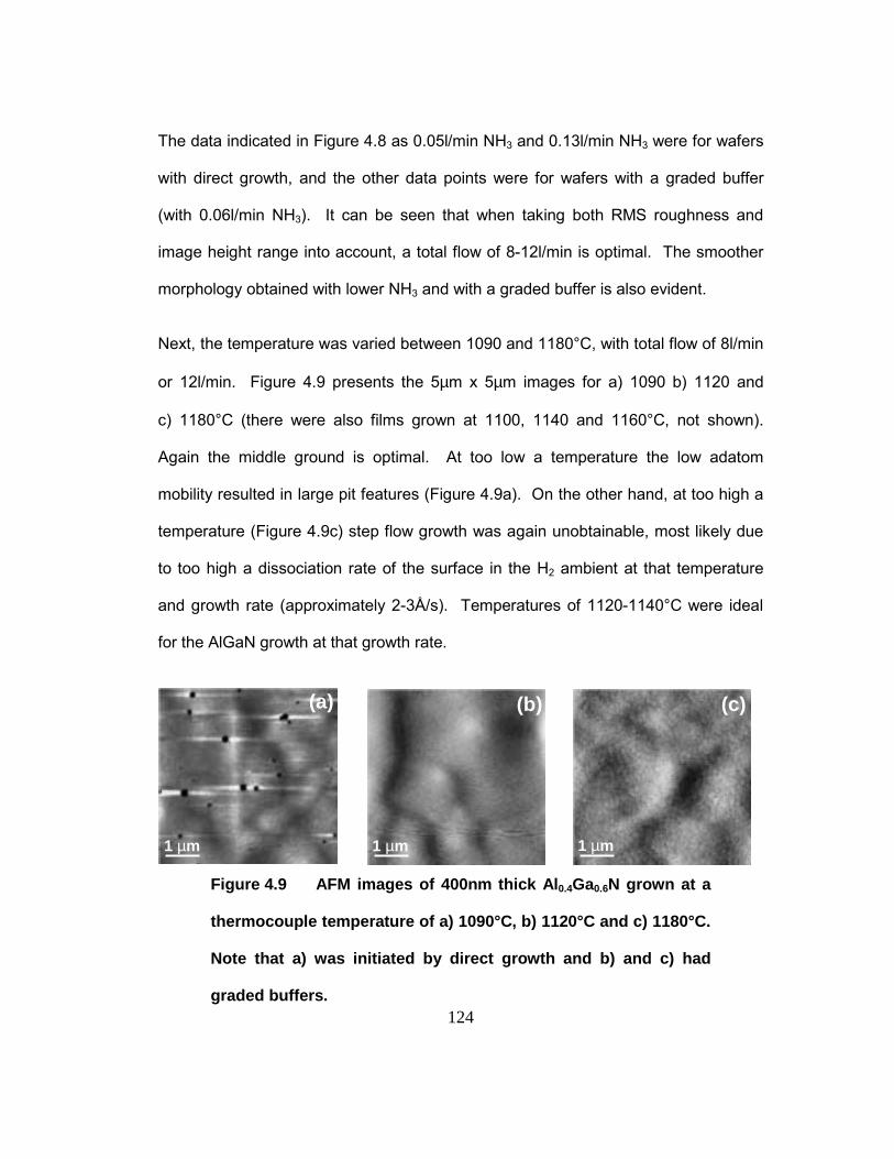
124
The data indicated in Figure 4.8 as 0.05l/min NH3 and 0.13l/min NH3 were for wafers
with direct growth, and the other data points were for wafers with a graded buffer
(with 0.06l/min NH3). It can be seen that when taking both RMS roughness and
image height range into account, a total flow of 8-12l/min is optimal. The smoother
morphology obtained with lower NH3 and with a graded buffer is also evident.
Next, the temperature was varied between 1090 and 1180°C, with total flow of 8l/min
or 12l/min. Figure 4.9 presents the 5µm x 5µm images for a) 1090 b) 1120 and
c) 1180°C (there were also films grown at 1100, 1140 and 1160°C, not shown).
Again the middle ground is optimal. At too low a temperature the low adatom
mobility resulted in large pit features (Figure 4.9a). On the other hand, at too high a
temperature (Figure 4.9c) step flow growth was again unobtainable, most likely due
to too high a dissociation rate of the surface in the H2 ambient at that temperature
and growth rate (approximately 2-3Å/s). Temperatures of 1120-1140°C were ideal
for the AlGaN growth at that growth rate.
1 µm 1 µm 1 µm
(b) (c)(a)
Figure 4.9 AFM images of 400nm thick Al0.4Ga0.6N grown at a
thermocouple temperature of a) 1090°C, b) 1120°C and c) 1180°C.
Note that a) was initiated by direct growth and b) and c) had
graded buffers.
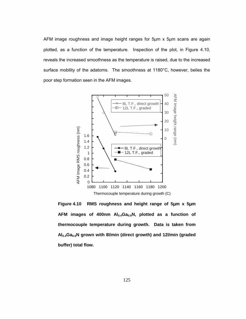
125
AFM image roughness and image height ranges for 5µm x 5µm scans are again
plotted, as a function of the temperature. Inspection of the plot, in Figure 4.10,
reveals the increased smoothness as the temperature is raised, due to the increased
surface mobility of the adatoms. The smoothness at 1180°C, however, belies the
poor step formation seen in the AFM images.
0
0.2
0.4
0.6
0.8
1
1.2
1.4
1.60
10
20
30
40
50
1080 1100 1120 1140 1160 1180 1200
8L T.F., direct growth12L T.F., graded
8L T.F., direct growth12L T.F., graded
AF
M Im
age
RM
S r
ough
ness
(nm
)
AF
M Im
age height range (nm)
Thermocouple temperature during growth (C)
Figure 4.10 RMS roughness and height range of 5µµµµm x 5µµµµm
AFM images of 400nm Al0.4Ga0.6N, plotted as a function of
thermocouple temperature during growth. Data is taken from
Al0.4Ga0.6N grown with 8l/min (direct growth) and 12l/min (graded
buffer) total flow.
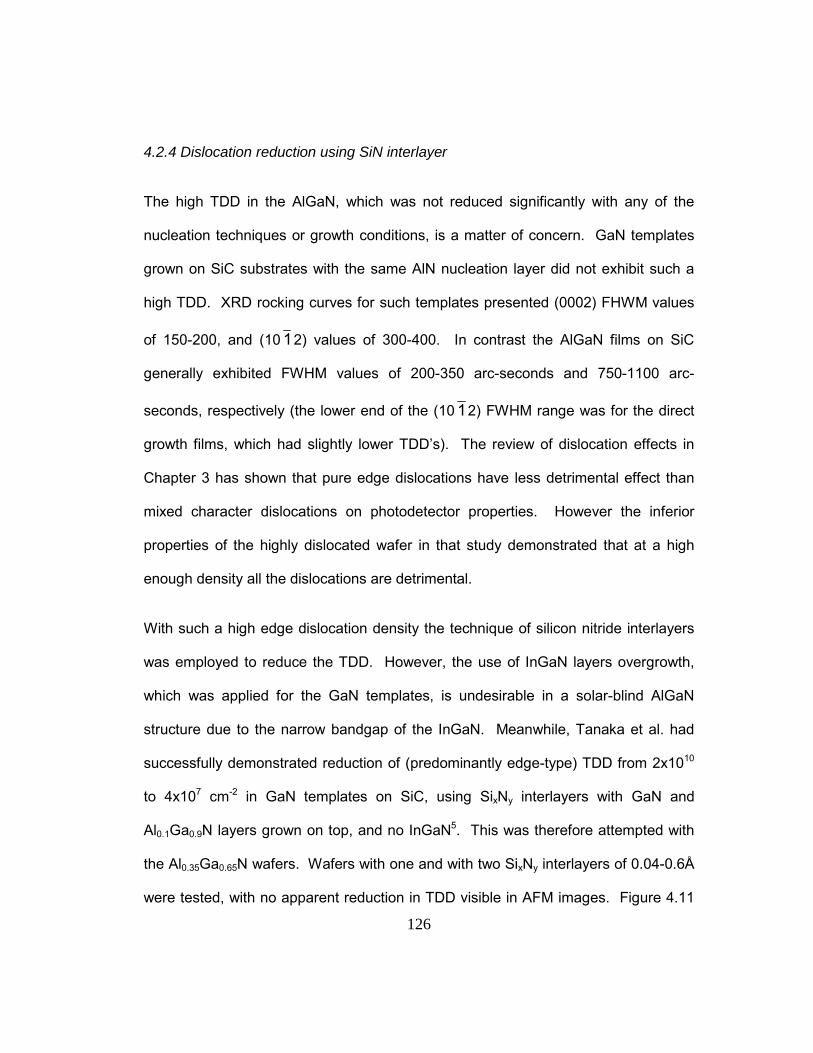
126
4.2.4 Dislocation reduction using SiN interlayer
The high TDD in the AlGaN, which was not reduced significantly with any of the
nucleation techniques or growth conditions, is a matter of concern. GaN templates
grown on SiC substrates with the same AlN nucleation layer did not exhibit such a
high TDD. XRD rocking curves for such templates presented (0002) FHWM values
of 150-200, and (10 12) values of 300-400. In contrast the AlGaN films on SiC
generally exhibited FWHM values of 200-350 arc-seconds and 750-1100 arc-
seconds, respectively (the lower end of the (10 12) FWHM range was for the direct
growth films, which had slightly lower TDD�s). The review of dislocation effects in
Chapter 3 has shown that pure edge dislocations have less detrimental effect than
mixed character dislocations on photodetector properties. However the inferior
properties of the highly dislocated wafer in that study demonstrated that at a high
enough density all the dislocations are detrimental.
With such a high edge dislocation density the technique of silicon nitride interlayers
was employed to reduce the TDD. However, the use of InGaN layers overgrowth,
which was applied for the GaN templates, is undesirable in a solar-blind AlGaN
structure due to the narrow bandgap of the InGaN. Meanwhile, Tanaka et al. had
successfully demonstrated reduction of (predominantly edge-type) TDD from 2x10¹⁰
to 4x107 cm-2 in GaN templates on SiC, using SixNy interlayers with GaN and
Al0.1Ga0.9N layers grown on top, and no InGaN5. This was therefore attempted with
the Al0.35Ga0.65N wafers. Wafers with one and with two SixNy interlayers of 0.04-0.6Å
were tested, with no apparent reduction in TDD visible in AFM images. Figure 4.11
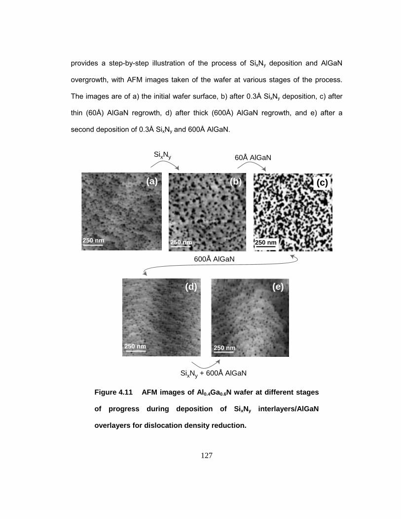
127
provides a step-by-step illustration of the process of SixNy deposition and AlGaN
overgrowth, with AFM images taken of the wafer at various stages of the process.
The images are of a) the initial wafer surface, b) after 0.3Å SixNy deposition, c) after
thin (60Å) AlGaN regrowth, d) after thick (600Å) AlGaN regrowth, and e) after a
second deposition of 0.3Å SixNy and 600Å AlGaN.
250 nm
(a)
250 nm 250 nm
(b) (c)
(e)(d)
250 nm250 nm
SixNy 60Å AlGaN
600Å AlGaN
SixNy + 600Å AlGaN
Figure 4.11 AFM images of Al0.4Ga0.6N wafer at different stages
of progress during deposition of SixNy interlayers/AlGaN
overlayers for dislocation density reduction.
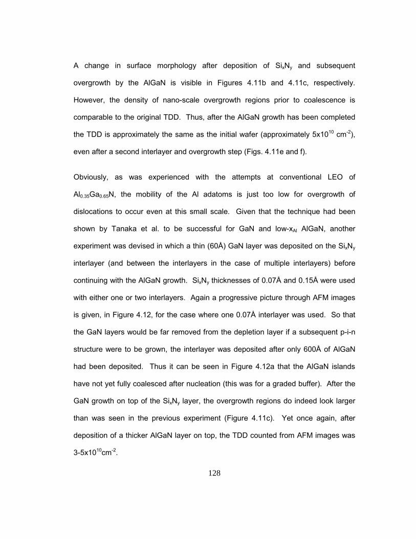
128
A change in surface morphology after deposition of SixNy and subsequent
overgrowth by the AlGaN is visible in Figures 4.11b and 4.11c, respectively.
However, the density of nano-scale overgrowth regions prior to coalescence is
comparable to the original TDD. Thus, after the AlGaN growth has been completed
the TDD is approximately the same as the initial wafer (approximately 5x1010 cm-2),
even after a second interlayer and overgrowth step (Figs. 4.11e and f).
Obviously, as was experienced with the attempts at conventional LEO of
Al0.35Ga0.65N, the mobility of the Al adatoms is just too low for overgrowth of
dislocations to occur even at this small scale. Given that the technique had been
shown by Tanaka et al. to be successful for GaN and low-xAl AlGaN, another
experiment was devised in which a thin (60Å) GaN layer was deposited on the SixNy
interlayer (and between the interlayers in the case of multiple interlayers) before
continuing with the AlGaN growth. SixNy thicknesses of 0.07Å and 0.15Å were used
with either one or two interlayers. Again a progressive picture through AFM images
is given, in Figure 4.12, for the case where one 0.07Å interlayer was used. So that
the GaN layers would be far removed from the depletion layer if a subsequent p-i-n
structure were to be grown, the interlayer was deposited after only 600Å of AlGaN
had been deposited. Thus it can be seen in Figure 4.12a that the AlGaN islands
have not yet fully coalesced after nucleation (this was for a graded buffer). After the
GaN growth on top of the SixNy layer, the overgrowth regions do indeed look larger
than was seen in the previous experiment (Figure 4.11c). Yet once again, after
deposition of a thicker AlGaN layer on top, the TDD counted from AFM images was
3-5x1010cm-2.
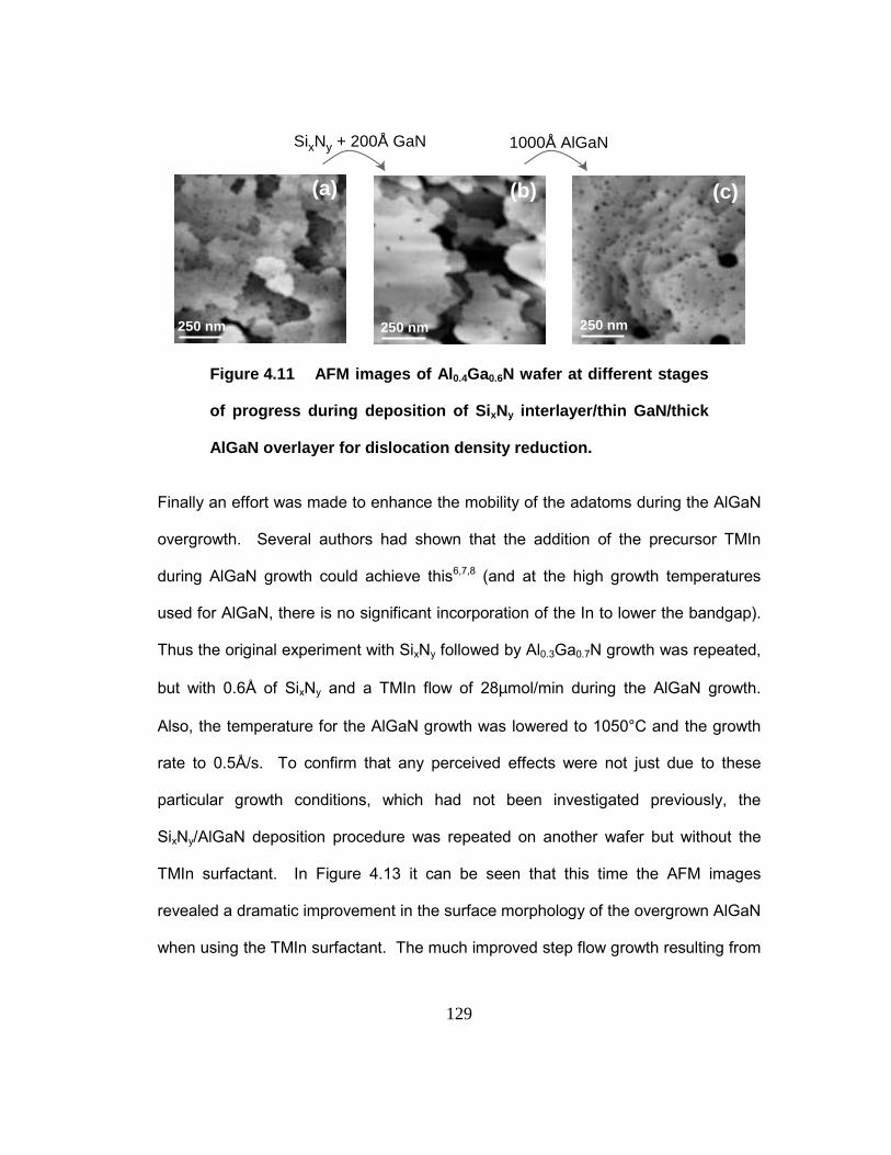
129
SixNy + 200Å GaN 1000Å AlGaN
(a) (b) (c)
250 nm 250 nm 250 nm
Figure 4.11 AFM images of Al0.4Ga0.6N wafer at different stages
of progress during deposition of SixNy interlayer/thin GaN/thick
AlGaN overlayer for dislocation density reduction.
Finally an effort was made to enhance the mobility of the adatoms during the AlGaN
overgrowth. Several authors had shown that the addition of the precursor TMIn
during AlGaN growth could achieve this6,7,8 (and at the high growth temperatures
used for AlGaN, there is no significant incorporation of the In to lower the bandgap).
Thus the original experiment with SixNy followed by Al0.3Ga0.7N growth was repeated,
but with 0.6Å of SixNy and a TMIn flow of 28µmol/min during the AlGaN growth.
Also, the temperature for the AlGaN growth was lowered to 1050°C and the growth
rate to 0.5Å/s. To confirm that any perceived effects were not just due to these
particular growth conditions, which had not been investigated previously, the
SixNy/AlGaN deposition procedure was repeated on another wafer but without the
TMIn surfactant. In Figure 4.13 it can be seen that this time the AFM images
revealed a dramatic improvement in the surface morphology of the overgrown AlGaN
when using the TMIn surfactant. The much improved step flow growth resulting from
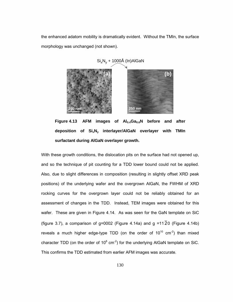
130
the enhanced adatom mobility is dramatically evident. Without the TMIn, the surface
morphology was unchanged (not shown).
SixNy + 1000Å (In)AlGaN
250 nm
(a)
250 nm
(b)
Figure 4.13 AFM images of Al0.4Ga0.6N before and after
deposition of SixNy interlayer/AlGaN overlayer with TMIn
surfactant during AlGaN overlayer growth.
With these growth conditions, the dislocation pits on the surface had not opened up,
and so the technique of pit counting for a TDD lower bound could not be applied.
Also, due to slight differences in composition (resulting in slightly offset XRD peak
positions) of the underlying wafer and the overgrown AlGaN, the FWHM of XRD
rocking curves for the overgrown layer could not be reliably obtained for an
assessment of changes in the TDD. Instead, TEM images were obtained for this
wafer. These are given in Figure 4.14. As was seen for the GaN template on SiC
(figure 3.7), a comparison of g=0002 (Figure 4.14a) and g =11 20 (Figure 4.14b)
reveals a much higher edge-type TDD (on the order of 1010 cm-2) than mixed
character TDD (on the order of 108 cm-2) for the underlying AlGaN template on SiC.
This confirms the TDD estimated from earlier AFM images was accurate.
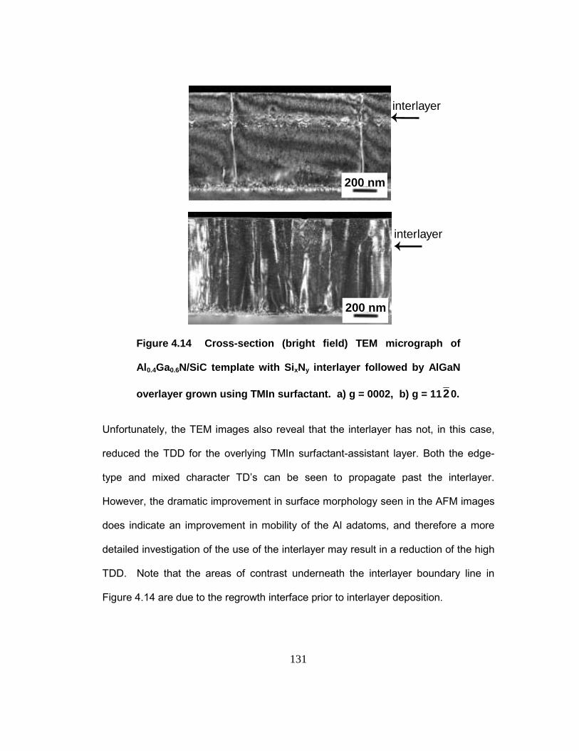
131
200 nm
200 nm
interlayer
interlayer
Figure 4.14 Cross-section (bright field) TEM micrograph of
Al0.4Ga0.6N/SiC template with SixNy interlayer followed by AlGaN
overlayer grown using TMIn surfactant. a) g = 0002, b) g = 1120.
Unfortunately, the TEM images also reveal that the interlayer has not, in this case,
reduced the TDD for the overlying TMIn surfactant-assistant layer. Both the edge-
type and mixed character TD�s can be seen to propagate past the interlayer.
However, the dramatic improvement in surface morphology seen in the AFM images
does indicate an improvement in mobility of the Al adatoms, and therefore a more
detailed investigation of the use of the interlayer may result in a reduction of the high
TDD. Note that the areas of contrast underneath the interlayer boundary line in
Figure 4.14 are due to the regrowth interface prior to interlayer deposition.
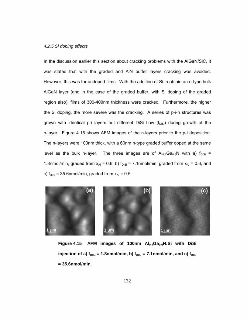
132
4.2.5 Si doping effects
In the discussion earlier this section about cracking problems with the AlGaN/SiC, it
was stated that with the graded and AlN buffer layers cracking was avoided.
However, this was for undoped films. With the addition of Si to obtain an n-type bulk
AlGaN layer (and in the case of the graded buffer, with Si doping of the graded
region also), films of 300-400nm thickness were cracked. Furthermore, the higher
the Si doping, the more severe was the cracking. A series of p-i-n structures was
grown with identical p-i layers but different DiSi flow (fDiSi) during growth of the
n-layer. Figure 4.15 shows AFM images of the n-layers prior to the p-i deposition.
The n-layers were 100nm thick, with a 60nm n-type graded buffer doped at the same
level as the bulk n-layer. The three images are of Al0.4Ga0.6N with a) fDiSi =
1.8nmol/min, graded from xAl = 0.6, b) fDiSi = 7.1nmol/min, graded from xAl = 0.6, and
c) fDiSi = 35.6nmol/min, graded from xAl = 0.5.
1 µm 1 µm 1 µm
(b) (c)(a)
Figure 4.15 AFM images of 100nm Al0.4Ga0.6N:Si with DiSi
injection of a) fDiSi = 1.8nmol/min, b) fDiSi = 7.1nmol/min, and c) fDiSi
= 35.6nmol/min.
133
A fourth wafer had fDiSi = 7.1nmol/min, graded from xAl = 0.5, and looked similar to b).
The third image, of the most highly doped film (Figure 4.15c) is strikingly different in
morphology to the others, and to the earlier undoped films. The surface is much
smoother, and the islands replaced by a larger scale undulation of film thickness.
After the p-i structures (400Å GaN:Mg + 4000Å Al0.4Ga0.6N) were deposited, the
structure which had this highly doped n- Al0.4Ga0.6N layer underneath was severely
cracked. The structures with fDiSi = 7.1nmol/min had only a few cracks, whilst the
structure with fDiSi = 1.8nmol/min had no cracks. Evidently the more doped films had
a higher tensile strain, which may be the reason for the change in morphology. This
was further confirmed by 2θ-ω XRD scans of the wafers. The higher the doping, the
further the AlGaN peak position was shifted to the right, indicating greater contraction
of the in-plane lattice constant (and therefore greater tensile strain). It was not an
indication of higher xAl content, as the SIMS investigations presented in Chapter 2
had shown that the addition of DiSi participates in the pre-reactions involving the
TMAl precursor, and therefore would not result in an enhancement of Al
incorporation.
4.3 AlGaN detectors on SiC
4.3.1 n-type doping of AlGaN
In order for a high field in the depletion region and efficient carrier diffusion in the
bulk p- and n- regions of the photodiode, the p- and n- regions should be reasonably
highly doped and not too resistive. This is why p-GaN was used for the diodes in this
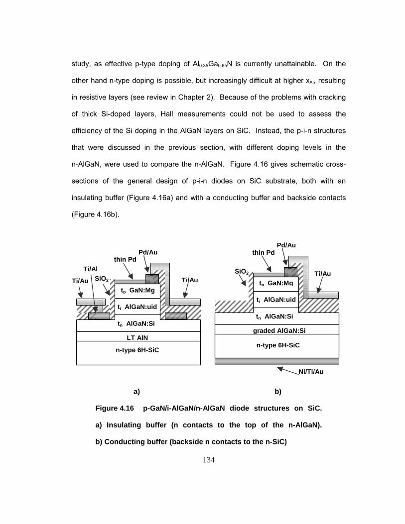
134
ti AlGaN:uid
tp GaN:Mg Ti/Au
Pd/Au
SiO2
n-type 6H-SiC
thin Pd
tn AlGaN:Si
Ti/Au
Ti/Al
LT AlN
ti AlGaN:uid
tp GaN:Mg Ti/Au
Pd/Au
SiO2
thin Pd
tn AlGaN:Si
graded AlGaN:Si
Ni/Ti/Au
n-type 6H-SiC
study, as effective p-type doping of Al0.35Ga0.65N is currently unattainable. On the
other hand n-type doping is possible, but increasingly difficult at higher xAl, resulting
in resistive layers (see review in Chapter 2). Because of the problems with cracking
of thick Si-doped layers, Hall measurements could not be used to assess the
efficiency of the Si doping in the AlGaN layers on SiC. Instead, the p-i-n structures
that were discussed in the previous section, with different doping levels in the
n-AlGaN, were used to compare the n-AlGaN. Figure 4.16 gives schematic cross-
sections of the general design of p-i-n diodes on SiC substrate, both with an
insulating buffer (Figure 4.16a) and with a conducting buffer and backside contacts
(Figure 4.16b).
a) b)
Figure 4.16 p-GaN/i-AlGaN/n-AlGaN diode structures on SiC.
a) Insulating buffer (n contacts to the top of the n-AlGaN).
b) Conducting buffer (backside n contacts to the n-SiC)
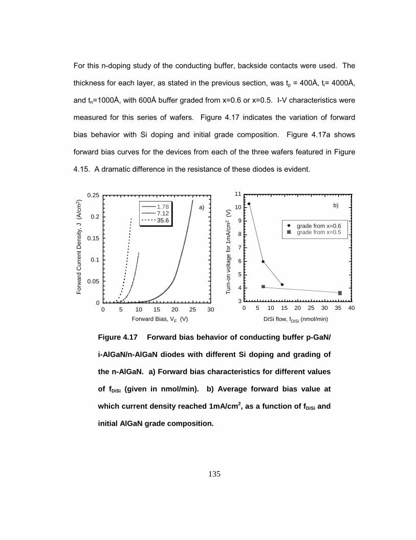
135
For this n-doping study of the conducting buffer, backside contacts were used. The
thickness for each layer, as stated in the previous section, was tp = 400Å, ti= 4000Å,
and tn=1000Å, with 600Å buffer graded from x=0.6 or x=0.5. I-V characteristics were
measured for this series of wafers. Figure 4.17 indicates the variation of forward
bias behavior with Si doping and initial grade composition. Figure 4.17a shows
forward bias curves for the devices from each of the three wafers featured in Figure
4.15. A dramatic difference in the resistance of these diodes is evident.
For
war
d C
urre
nt D
ensi
ty, J
(A
/cm
2 )
Forward Bias, VF (V)
0
0.05
0.1
0.15
0.2
0.25
0 5 10 15 20 25 30
1.787.1235.6
a)
3
4
5
6
7
8
9
10
11
0 5 10 15 20 25 30 35 40
grade from x=0.6grade from x=0.5
DiSi flow, fDiSi (nmol/min)
Tur
n-on
vol
tage
for
1mA
/cm
2 (
V)
b)
Figure 4.17 Forward bias behavior of conducting buffer p-GaN/
i-AlGaN/n-AlGaN diodes with different Si doping and grading of
the n-AlGaN. a) Forward bias characteristics for different values
of fDiSi (given in nmol/min). b) Average forward bias value at
which current density reached 1mA/cm2, as a function of fDiSi and
initial AlGaN grade composition.
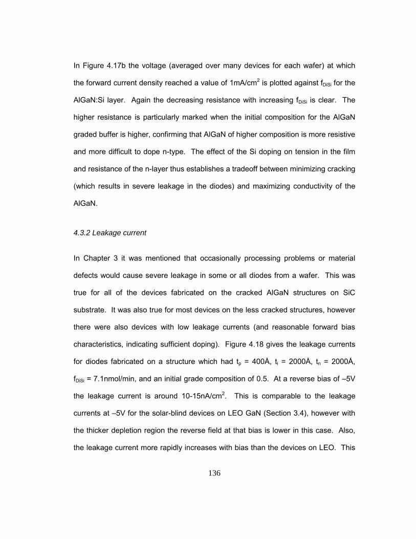
136
In Figure 4.17b the voltage (averaged over many devices for each wafer) at which
the forward current density reached a value of 1mA/cm2 is plotted against fDiSi for the
AlGaN:Si layer. Again the decreasing resistance with increasing fDiSi is clear. The
higher resistance is particularly marked when the initial composition for the AlGaN
graded buffer is higher, confirming that AlGaN of higher composition is more resistive
and more difficult to dope n-type. The effect of the Si doping on tension in the film
and resistance of the n-layer thus establishes a tradeoff between minimizing cracking
(which results in severe leakage in the diodes) and maximizing conductivity of the
AlGaN.
4.3.2 Leakage current
In Chapter 3 it was mentioned that occasionally processing problems or material
defects would cause severe leakage in some or all diodes from a wafer. This was
true for all of the devices fabricated on the cracked AlGaN structures on SiC
substrate. It was also true for most devices on the less cracked structures, however
there were also devices with low leakage currents (and reasonable forward bias
characteristics, indicating sufficient doping). Figure 4.18 gives the leakage currents
for diodes fabricated on a structure which had tp = 400Å, ti = 2000Å, tn = 2000Å,
fDiSi = 7.1nmol/min, and an initial grade composition of 0.5. At a reverse bias of �5V
the leakage current is around 10-15nA/cm2. This is comparable to the leakage
currents at �5V for the solar-blind devices on LEO GaN (Section 3.4), however with
the thicker depletion region the reverse field at that bias is lower in this case. Also,
the leakage current more rapidly increases with bias than the devices on LEO. This
137
dislocation-induced soft breakdown indicates that at such high densities of 1010 cm-2,
even the edge dislocations are contributing to the leakage in the devices.
10-10
10-9
10-8
10-7
10-6
10-5
10-4
-20 -15 -10 -5 0
Leak
age
Cur
rent
, JL
(A/c
m2 )
Reverse Bias, VR (V)
Figure 4.18 Best leakage current densities for conducting
buffer p-GaN/i-AlGaN/n-AlGaN diodes on SiC substrate.
4.3.3 Spectral response
Diode structures were grown on SiC with and without a conducting buffer, for
comparison of spectral response. Figure 4.19 shows the current responsivity for
diodes fabricated on two p-i-n structures with a conducting buffer (see diode
schematic in Figure 4.16b). They both have tp = 400Å and ti = 2000Å. They differed
in thickness of the n-layer above the graded buffer - one had tn = 1000Å and the
other had tn = 2000Å. It is important to keep in mind that the thickness of the n-layer
is representative of the proximity of the i-layer to the SiC (tn+600Å). It is obvious that
the magnitude of the photoresponse of the devices on SiC is significantly less than
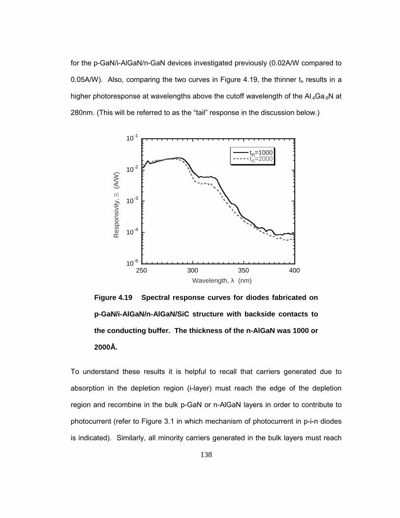
138
for the p-GaN/i-AlGaN/n-GaN devices investigated previously (0.02A/W compared to
0.05A/W). Also, comparing the two curves in Figure 4.19, the thinner tn results in a
higher photoresponse at wavelengths above the cutoff wavelength of the Al.4Ga.6N at
280nm. (This will be referred to as the �tail� response in the discussion below.) R
espo
nsiv
ity, R
(A
/W)
Wavelength, λ (nm)
10-5
10-4
10-3
10-2
10-1
250 300 350 400
tn=1000tn=2000
Figure 4.19 Spectral response curves for diodes fabricated on
p-GaN/i-AlGaN/n-AlGaN/SiC structure with backside contacts to
the conducting buffer. The thickness of the n-AlGaN was 1000 or
2000Å.
To understand these results it is helpful to recall that carriers generated due to
absorption in the depletion region (i-layer) must reach the edge of the depletion
region and recombine in the bulk p-GaN or n-AlGaN layers in order to contribute to
photocurrent (refer to Figure 3.1 in which mechanism of photocurrent in p-i-n diodes
is indicated). Similarly, all minority carriers generated in the bulk layers must reach
139
and traverse the depletion layer and recombine as majority carriers in the bulk layer
on the other side of the depletion region.
The i-layer in these devices is four times the thickness of the i-layer in the p-GaN/
i-AlGaN/n-GaN devices, and it was expected that these devices would have a higher
responsivity due to the greater absorbing region. However this is not the case �
implying that less of the absorption in these structures contributes to photocurrent. It
is also true that the p-GaN is thicker in this case than for the earlier structures,
however there are no quantum wells to impede the minority electron flow into the
AlGaN depletion region so this should not be a significant cause of the low
responsivity. It is apparent, therefore, that a high proportion of the photogenerated
carriers are recombining before they can traverse the depletion region. A high
recombination rate suggests that the AlGaN is of poor electrical quality.
Another diode structure was grown with tp = 400Å, ti = 4000Å and tn = 1000Å. Again,
if the photogenerated carriers were being efficiently transported across the depletion
region, this structure, with a thicker total absorbing region, should have had a higher
peak photoresponse. Instead the responsivity was lower still. This further indicates
that there is a high incidence of recombination or trapping of carriers in the depletion
region. The thicker the depletion region, the more chance of recombination or
trapping occurring before the photogenerated carriers can reach the bulk layers.
This third structure also exhibited less of the tail response seen in Figure 4.19, at
wavelengths to which the AlGaN is transparent. The tail is most likely due to
absorption in the underlying SiC, which has a bandgap energy of 2.9eV. The thicker
140
the total AlGaN, the more there will be recombination of photogenerated holes from
the SiC before they can traverse the i-layer and recombine in the p-GaN.
The thickness of the n-layer with a conducting buffer was limited to 2000Å due to
tension introduced by the Si-doping. Thus the tail response could not be reduced by
increasing tn instead of ti. Instead, diodes were fabricated on a structure with an
insulating buffer. Such devices were indicated schematically in Figure 4.16a. These
diodes had tp = 250Å, ti = 2000Å and tn = 2000Å. Due to temperature drift in the
reactor the composition was a little lower than intended, with xAl = 0.3. The insulating
buffer was 0.4µm thick, and consisted of a 200Å AlN nucleation layer followed by a
4000Å grade to Al0.3Ga0.7N. For comparison to the p-GaN/i-AlGaN/n-GaN diodes in
Chapter 2 the p-layer consisted of p-GaN/p-Al0.1Ga0.9N quantum wells with a p-GaN
cap. The spectral response is given in Figure 4.20.
It can be seen that with the insulating buffer the spectral response is much improved
compared to the conducting buffer structures. The tail due to absorption in the SiC is
significantly reduced. Note that the tail is somewhat jagged; this is measurement
noise due to insufficient averaging time during measurements. The peak
responsivity is 0.08A/W at a wavelength of 292nm, corresponding to an external
quantum efficiency of 35%. The optical quality of the AlGaN in the depletion layer
has been significantly improved by the addition of the 0.5µm insulating buffer. This
large increase in separation of the depletion region from the substrate (and
nucleation region) has obviously greatly reduced the optically denigrating defect
content in the material.
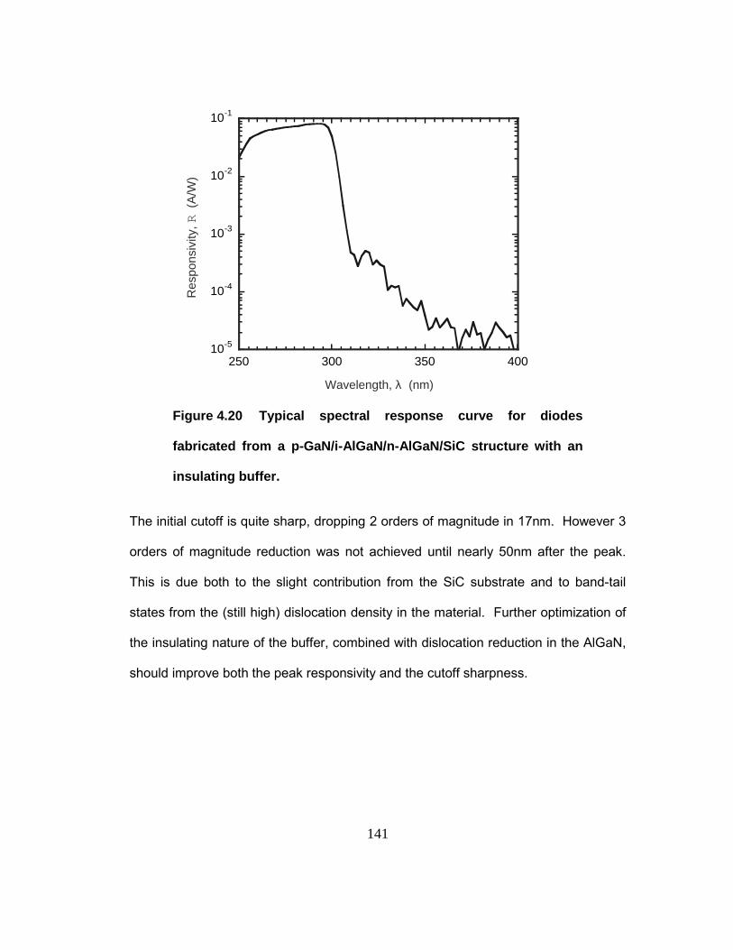
141
10-5
10-4
10-3
10-2
10-1
250 300 350 400
Wavelength, λ (nm)
Res
pons
ivity
, R (
A/W
)
Figure 4.20 Typical spectral response curve for diodes
fabricated from a p-GaN/i-AlGaN/n-AlGaN/SiC structure with an
insulating buffer.
The initial cutoff is quite sharp, dropping 2 orders of magnitude in 17nm. However 3
orders of magnitude reduction was not achieved until nearly 50nm after the peak.
This is due both to the slight contribution from the SiC substrate and to band-tail
states from the (still high) dislocation density in the material. Further optimization of
the insulating nature of the buffer, combined with dislocation reduction in the AlGaN,
should improve both the peak responsivity and the cutoff sharpness.
142
4.4 Conclusions
Use of GaN for the n-layer in a solar-blind p-i-n detector (with Al0.35Ga0.65N for the i-
layer) results in non-solar-blind broadening of the spectral cutoff. Bulk AlGaN growth
enables use of an n-AlGaN layer and also a thicker i-AlGaN layer for higher
responsivity. Growth of bulk AlGaN on SiC requires careful optimization of the
nucleation conditions to achieve a balance between the compressive lattice
mismatch and the tensile thermal mismatch. Si doping introduces further tensile
strain. The bulk AlGaN grown on SiC has a high edge-type TDD, much higher than
GaN grown on SiC. The smoothest surface morphologies were obtained with a total
flow of 8-12 l/min, thermocouple temperature of 1120-1140°C, and NH3 flow of
0.5 l/min. Surface morphology could be significantly improved when TMIn was used
as a surfactant to enhance the mobility of the Al adatoms during AlGaN growth.
The p-GaN/i-AlGaN/n-AlGaN diodes on SiC substrate exhibited reasonably low
leakage currents and high responsivity. With a conducting buffer the diodes
exhibited non-solar-blind spectral response due to absorption in the SiC. With an
insulating buffer this tail response was almost eliminated. The TDD must be reduced
to further improve the photodiode properties. The use of a SixNy interlayer for TDD
reduction was not successful in the studies presented here but combining this
technique with the TMIn surfactant effect bears promise for future efforts.
143
4.5 References
1. T. Akasaka, Y. Kobayashi, S. Ando, N. Kobayashi, and M. Kumagai, �Selective
MOVPE of GaN and AlxGa1-xN with smooth vertical facets.� J. Cryst. Growth 189/190, 72-77
(1998).
2. M.D. Bremser, W.G. Perry, T. Zhevela, N.V. Edwards, O.H. Nam, N. Parikh, D.E.
Aspnes, and Robert F. Davis, �Growth, doping and characterization of AlxGa1-xN thin film
alloys on 6H-SiC(0001) substrates.� MRS Internet J. Nitride Semicond. Res. 1, 8 (1996).
3. P. Waltereit, O. Brandt, A. Trampert, M. Ramsteiner, M. Reiche, M. Qi, and K.H.
Ploog �Influence of AlN nucleation layers on growth mode and strain relief of GaN grown on
6H-SiC(0001).� Appl. Phys. Lett. 74, 3660-3662 (1999).
4. H. Lahrèche, M. Leroux, M. Laügt, M. Vaille, B. Beaumont, and P. Gibart �Buffer free
growth of GaN on 6H-SiC by metalorganic vapor phase epitaxy.� J. Appl.Phys. 87, 577-583
(2000).
5. S. Tanaka, M. Takeuchi, and Y. Aoyagi �Anti-surfactant in III-nitride epitaxy �
quantum dot formation and dislocation termination-.� Jpn. J. Appl. Phys. 39, 831-834 (2000).
6. C.K. Shu, J. Ou, H.C. Lin, W.K. Chen and M.C. Lee, �Isoelectronic In-doping effect in
GaN films grown by metalorganic chemical vapor deposition.� Appl. Phys. Lett. 73, 641-643
(1998).
7. S. Yamaguchi, M. Kariya, S. Nitta, H. Amano, and I. Akasaki, �Strain relief and its
effect on the properties of GaN using isoelectronic In doping grown by metalorganic vapor
phase epitaxy.� Appl. Phys. Lett. 75, 4106-4108 (1999).
8. G. Pozina, J.P. Bergman, B. Monemar, S. Yamaguchi, H. Amano, and I. Akasaki,
�Optical spectroscopy of GaN grown by metalorganic vapor phase epitaxy using indium
surfactant.� Appl. Phys. Lett. 76, 3388-3390 (2000).
144
Chapter 5. Conclusions and future work.
With AlxGa1-xN-based material and device technology still at an early stage of
development, the studies presented here have resulted in unmistakable
advancements in the growth of AlGaN and in knowledge of critical aspects of
ultraviolet detector performance and design. Further work, including the
recommendations detailed later in this chapter, will certainly lead to yet more
advancements and improve upon the detector results presented here.
5.1 AlGaN growth on sapphire substrate.
The studies into AlxGa1-xN (xAl ≥ 0.3) growth emphasized that achievement of
smooth, defect-free AlGaN (regardless of the substrate and/or underlying layers) is
substantially more difficult than for GaN grown by MOCVD. This is due in no small
way to the low mobility of Al adatoms on the epitaxial surface, to pre-reactions which
necessitate low growth pressures, and to the high bond strength of Al to impurities
and to substrate and mask constituents (notably O, C and N).
The studies conclusively demonstrated the tendency of increased defect formation
with increasing Al content and increasing strain in the AlGaN layer. When grown on
GaN templates the strain increases with xAl due to the increase in lattice mismatch.
Too much strain can result in the occurrence of cracking � this occurs during growth
and not after cooldown, and is therefore due to the lattice and not the thermal
mismatch. The presence of dislocations in the underlying template also enhances
defect formation in the AlGaN.
145
Improvement of the AlGaN morphology and a first-order reduction of the defects
requires maximization of surface mobility during growth. It was found that this could
be achieved by reducing nitrogen overpressure by reducing NH3 flow. Thereby the
effect of increasing defect formation with Al content could be counteracted, resulting
in AlGaN that more resembled GaN in surface morphology for thin AlGaN layers
grown on GaN templates. Reduction of threading dislocations by LEO completed
this transformation to a low-defect GaN-like morphology.
In addition to extended defects, point defects due to impurity incorporation in GaN
and AlGaN are ever-present. SIMS investigations of C and O content showed they
could be reduced, by optimizing growth conditions, such as by raising the growth
temperature. Incorporation unavoidably increases with Al content though, due to the
aforementioned high bond strengths of Al to O and C.
Attempts using non-traditional mask materials for LEO of AlxGa1-xN (in addition to the
traditional mask material SiO2) were unsuccessful, with no selectivity achieved for
SiO2, sapphire, Pt and TiN masks. Again this is due to the high sticking probability
and low mobility of the Al adatoms, on both the masked and unmasked surfaces.
5.2 AlGaN on SiC.
For bulk AlGaN growth on SiC, the initial growth on the substrate will determine
whether the (compressive) lattice mismatch will balance the (tensile) thermal
mismatch. If the lattice mismatch is relieved too much during growth the residual
tensile strain will cause cracking, at a thickness insufficient for device purposes
146
(<0.5µm). This occurred for direct growth of AlGaN at high temperature and fast
growth rate (2-3Å/s). Initiating the growth with a slow growth rate AlN layer (grown at
a lower temperature) or graded AlGaN layer (gradually ramped to bulk composition
and growth rate) resulted in less residual tensile strain and no cracking.
Unlike the thin layers on GaN templates, the bulk AlGaN layers grown under reduced
NH3 conditions did not show a GaN-like morphology (compared to GaN templates
grown on SiC with an AlN nucleation layer). The surface morphology was
characterized by large islands which were1-5µm in diameter (with step flow growth
on and between the islands). The TDD was also much higher than for the GaN
templates, with (mostly edge-type) TDD�s of 2-5x1010 cm-2.
Once more the low surface mobility of the Al adatoms interfered with TDD reduction
techniques. Use of a SixNy submonolayer, which masks edge dislocations and can
result in subsequent reduction of the edge dislocations in overgrown layers, did not
work when overgrown with AlGaN. The use of TMIn as a surfactant to enhance the
mobility shows promise for improvement of surface morphology and reduction in
TDD of the overgrown AlGaN.
The addition of Si to thick AlGaN layers grown on SiC substrate increases tension in
the layers and causes cracking. Yet with the resistance of the AlxGa1-xN increasing
as xAl increases, higher Si doping is needed for n-type conductivity for p-i-n
photodiodes. A tradeoff ensues between n-layer thickness and conductivity, and
cracking, for p-i-n AlGaN structures on SiC substrate.
147
5.3 Dislocations and photodiodes
The investigations into the effect of threading dislocations on GaN and AlGaN
photodiodes revealed unequivocally that they are detrimental to detector
performance. This study was performed primarily with GaN p-i-n photodiodes grown
on GaN templates of various TD compositions and densities.
GaN (and its alloys) when epitaxially grown on sapphire have a high mixed and edge
TDD. Optimization of the nucleation conditions can reduce the TDD from 109-1010
cm-2 to low-mid-108 cm-2. We used several approaches for further dislocation
reduction. The use of a submonolayer silicon nitride (SixNy) interlayer overgrown
with thin InGaN layers appears to reduce the edge-type TDD. Growth on SiC
substrate reduces the mixed-type TDD. LEO GaN has a dramatically reduced TDD,
both mixed and edge character.
The studies showed that the presence of edge dislocations has less effect than
mixed on leakage current and spectral broadening. That is, a much bigger decrease
in leakage current can be obtained by reducing mixed- than by reducing edge-type
TDD�s. However, reducing edge-type TDD from very high levels (high being109-1010
cm-2) does have an effect.
Growth of photodiodes on LEO GaN results in the lowest leakage currents, due to
the very low overall TDD. Yet spectral broadening of the GaN photodiode response
was a little worse, possibly due to impurities from the SiO2 mask material. Impurities
in the overgrown GaN originating from the mask are an issue that still requires some
treatment in LEO studies. Furthermore, although it is reduced, there is still
148
significant leakage current when LEO is used, higher than would be expected in
photodiodes with such a wide bandgap.
Measurements of leakage current in GaN photodiodes with a reduced TDD revealed
that it is at least partly due to defects in the i-layer. This layer is highly compensated.
The leakage current is not due in any part to the sidewalls � devices with and without
passivation, and with different perimeter-to-area ratios, did not exhibit differences in
leakage currents. This was true even when the TDD was not reduced by LEO.
In a p-GaN/i-Al0.33Ga0.67N/n-GaN structure designed to prevent photogenerated
carrier movement from p- and n-GaN to the i-AlGaN (for solar-blind behavior), again
the TD�s were found to increase leakage current and broaden the spectral response.
In this case the TD�s cause additional broadening of the solar-blind cutoff, by
enabling a larger photocurrent contribution from absorption in the GaN. Speed
measurements showed that TD�s (both edge- and mixed-type) also contribute to a
slow tail in the speed response (the pulsed response was the combination of a fast
and a slow exponential decay, except on the LEO wing).
5.4 Solar-blind detectors
The p-GaN/i-AlGaN/n-GaN structure has two major drawbacks - the broadening of
solar-blind cutoff due to contribution from absorption in the GaN, particularly in
presence of TDD, and the limitation of the i-AlGaN thickness to 500Å to avoid
cracking, which allows a peak responsivity of only 0.05 A/W (external quantum
efficiency of only 22%). Experiments showed that the broadening is due to holes
149
from n-GaN, which combined with the requirement of thicker i-AlGaN necessitates an
n-AlGaN buffer for solar-blind p-i-n diode design.
LEO of high-xAl AlGaN was not found to be possible, with four mask materials
investigated. SiC substrate was therefore chosen for development of thick AlGaN.
The benefits of improved detector performance should outweigh the increased
substrate cost. Although the TDD for the bulk AlGaN on SiC was very high it
consisted mostly of edge-type dislocations. Thus, solar-blind diodes on SiC
substrate exhibit relatively low leakage currents at moderate fields.
The employment of a conducting buffer to enable use of ohmic contacts to the n-type
SiC instead of to the n-AlGaN resulted in substantial photocurrent from the SiC. The
thickness limitations of the conducting buffer due to the tensile strain introduced by
the Si-doping meant that the i-layer was too close to the SiC.
With an insulating buffer, p-GaN/i-Al0.3Ga0.7N/n-Al0.3Ga0.7N diodes were fabricated
which exhibited good detector characteristics. The peak responsivity was 0.08A/W
at 292nm (quantum efficiency of 35%), with a 3 orders of magnitude drop within
50nm. These detectors have a better responsivity but slightly worse cutoff
characteristics and leakage currents compared to the p-GaN/i-Al0.33Ga0.67N/n-GaN
photodiodes. Thicker i-AlGaN layers resulted in decreased responsivity due to the
high recombination rates in the highly defective AlGaN.
150
5.5 Future work.
Improvement of the solar-blind detectors presented here requires first and foremost a
reduction in the defect density of the AlGaN. Although growth on SiC substrate does
reduce the mixed-type TDD, the edge-type TDD must be reduced below the present
levels of 1010 cm-2. Optimization of the SiN interlayer technique with TMIn surfactant
shows potential and should be developed further � only initial studies were carried
out in this work. Furthermore, reduction of the point defects by reduction of the
impurities present in the MOCVD system (given that the growth conditions cannot be
altered further due to surface morphology and pre-reaction restrictions) is necessary.
Additional defect reduction will be attained if a thicker buffer layer can be grown prior
to deposition of the p-i-n structure. The detectors fabricated with the AlN nucleation
layer had 0.5µm of insulating AlGaN, graded from AlN to Al0.3Ga0.7N, underneath the
p-i-n structure. Optimization of both the AlN and the graded layer should enable this
insulating layer to be made thicker without cracking the p-i-n structure. Furthermore,
with a thick higher-xAl buffer narrow-band spectral response could be achieved with
backside illumination. This also holds true for growth on sapphire substrates. With
defect reduction, perhaps using a combination of the SixNy/TMIn surfactant technique
for the edge-type dislocations and the low-temperature AlN interlayer pioneered by
Amano et al.1 for the mixed-type dislocations, low-defect density bulk AlGaN with a
higher-xAl buffer layer could be grown on sapphire substrates too. Recent results
have certainly shown that the use of a higher-xAl buffer layer alone, epitaxially grown
AlGaN of relatively high quality can be obtained2,3.
151
Finally, preliminary temperature-dependent studies of the defect levels causing
leakage current in the absence of threading dislocations were inconclusive and
therefore not included in this work. A thorough study is required, with temperature
both increased above and decreased below room temperature. Other temperature-
dependent techniques should also be used, such as deep level transient
spectroscopy, in order to pinpoint changes in defect levels with.
5.6 References
1. H. Amano, M. Iwaya, N. Hayashi, T. Kashima, S. Nitta, C. Wetzel, and I. Akasaki,
�Control of dislocations and stress in AlGaN on sapphire using a low temperature interlayer.�
Phys. Stat. Sol. (b) 216, 683-689 (1999).
2. U. Karrer, A. Dobner, O. Ambacher, and M. Stutzmann, �AlGaN-based ultraviolet light
detectors with integrated optical filters.� J. Vac. Sci. Technol.B 18, 757-760 (2000).
3. D.H. Lambert, M.M. Wong, U. Chowdhury, C. Collins, T. Li, K. Kwon, B.S. Shelton,
T.G. Zhu, J.C. Campbell, and R.D. Dupuis, �Back illuminated AlGaN solar-blind
photodetectors.� Appl. Phys. Lett. 77, 1090-1092 (2000)
152
Appendix A. Introduction to dislocations
A thorough introduction to the concept of defects is given in the book �Introduction to
Dislocations� by Derek Hull1, and is summarized here.
A.1 Crystal models
Crystal structures can be described in many ways. The atoms comprising the crystal
can, for example, be considered as points (the atomic core positions) or as spheres,
encompassing the entire spatial extent of each atom. Each of these representations
is useful in coming to an understanding of crystal defects. We consider first the
crystal lattice model. The lattice is made up of points (representing atoms) and lines
(representing bonds), and each lattice formation can be described in terms of a
unique unit cell. The unit cell is the smallest division of the lattice into repeated,
identical parallelepipeds. Alternatively, with the sphere model, the crystal can be
considered as a stack of atomic layers. The crystal is then uniquely identified by
description of the atomic arrangement within a layer and the placement of
consecutive layers relative to each other. Figure A.1 gives examples of unit cells
and of an ABAB� stacking sequence.
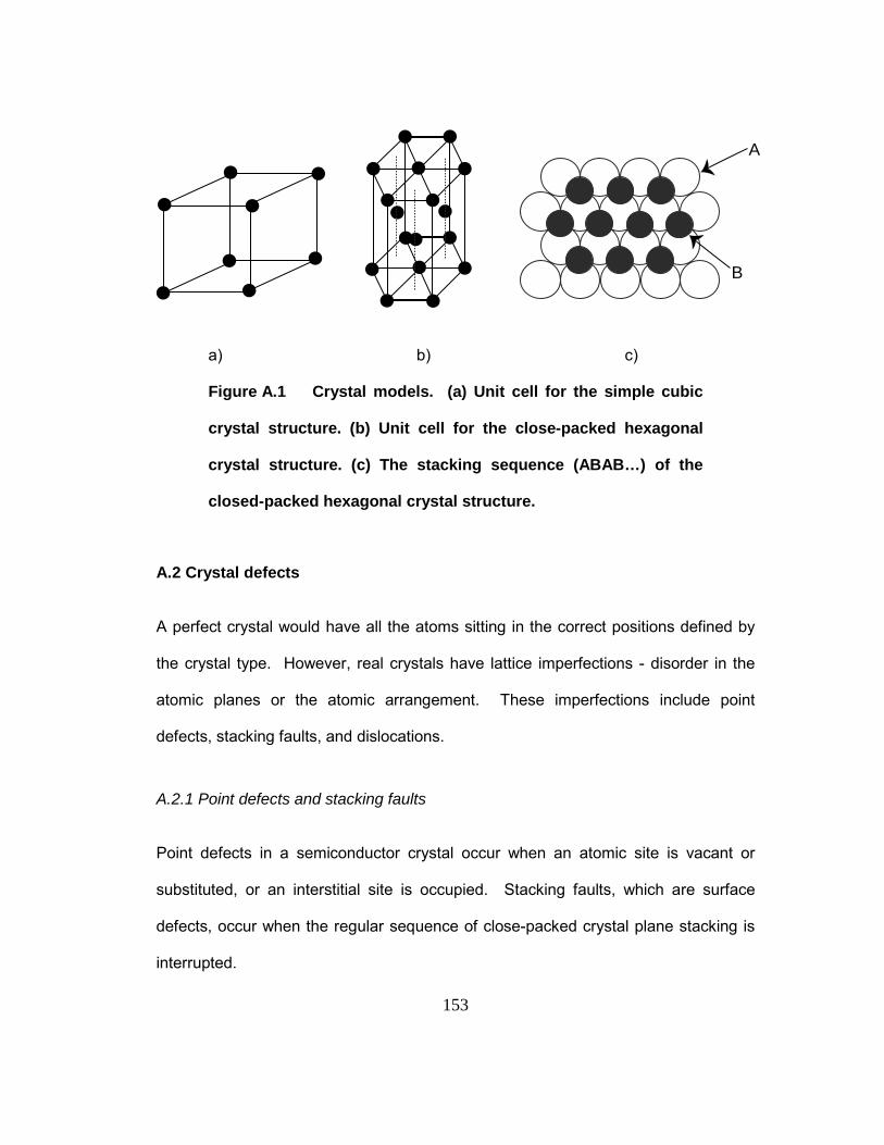
153
B
A
a) b) c)
Figure A.1 Crystal models. (a) Unit cell for the simple cubic
crystal structure. (b) Unit cell for the close-packed hexagonal
crystal structure. (c) The stacking sequence (ABAB…) of the
closed-packed hexagonal crystal structure.
A.2 Crystal defects
A perfect crystal would have all the atoms sitting in the correct positions defined by
the crystal type. However, real crystals have lattice imperfections - disorder in the
atomic planes or the atomic arrangement. These imperfections include point
defects, stacking faults, and dislocations.
A.2.1 Point defects and stacking faults
Point defects in a semiconductor crystal occur when an atomic site is vacant or
substituted, or an interstitial site is occupied. Stacking faults, which are surface
defects, occur when the regular sequence of close-packed crystal plane stacking is
interrupted.
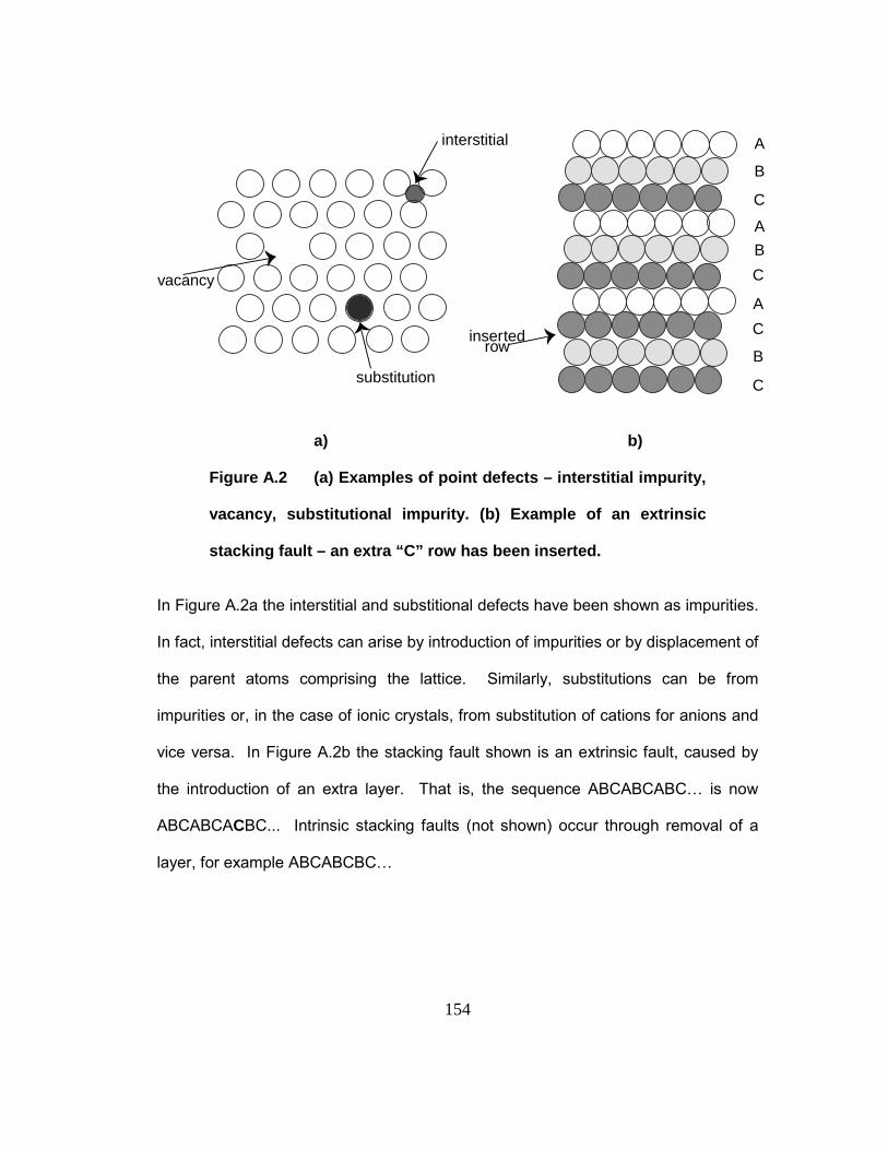
154
interstitial
substitution
vacancy
A
B
C
A
A
B
B
C
C
C
insertedrow
a) b)
Figure A.2 (a) Examples of point defects – interstitial impurity,
vacancy, substitutional impurity. (b) Example of an extrinsic
stacking fault – an extra “C” row has been inserted.
In Figure A.2a the interstitial and substitional defects have been shown as impurities.
In fact, interstitial defects can arise by introduction of impurities or by displacement of
the parent atoms comprising the lattice. Similarly, substitutions can be from
impurities or, in the case of ionic crystals, from substitution of cations for anions and
vice versa. In Figure A.2b the stacking fault shown is an extrinsic fault, caused by
the introduction of an extra layer. That is, the sequence ABCABCABC� is now
ABCABCACBC... Intrinsic stacking faults (not shown) occur through removal of a
layer, for example ABCABCBC�
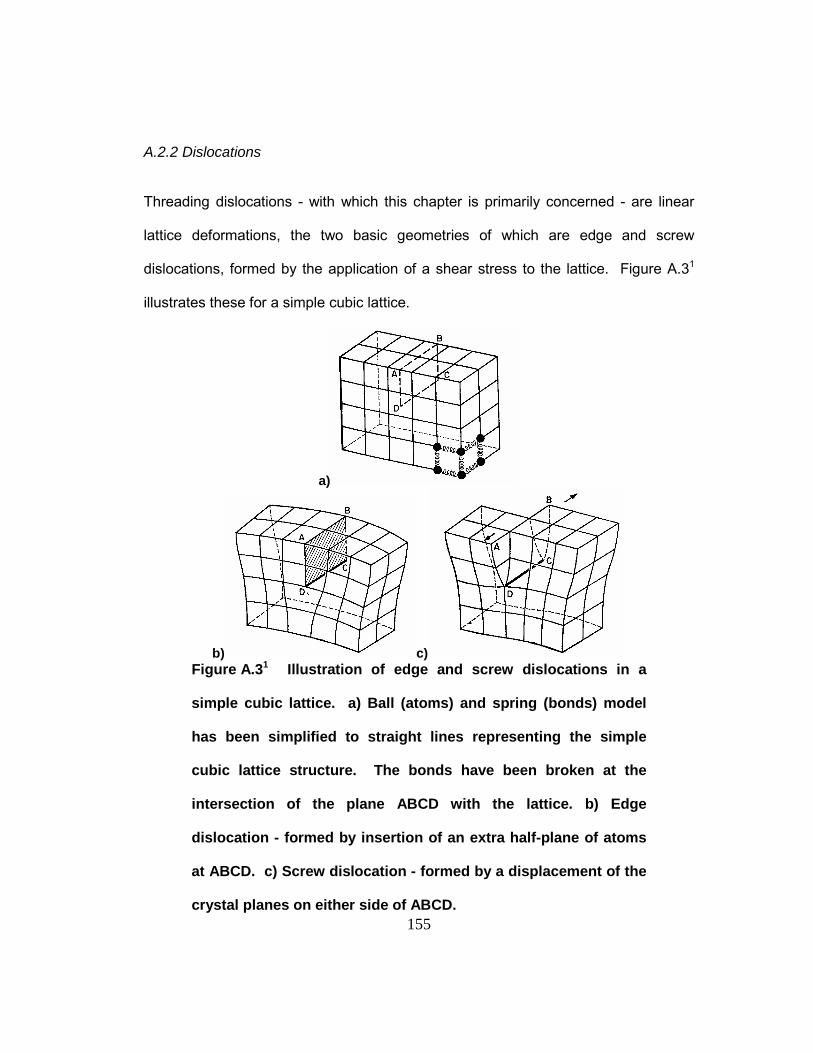
155
A.2.2 Dislocations
Threading dislocations - with which this chapter is primarily concerned - are linear
lattice deformations, the two basic geometries of which are edge and screw
dislocations, formed by the application of a shear stress to the lattice. Figure A.31
illustrates these for a simple cubic lattice.
a)
b) c) Figure A.31 Illustration of edge and screw dislocations in a
simple cubic lattice. a) Ball (atoms) and spring (bonds) model
has been simplified to straight lines representing the simple
cubic lattice structure. The bonds have been broken at the
intersection of the plane ABCD with the lattice. b) Edge
dislocation - formed by insertion of an extra half-plane of atoms
at ABCD. c) Screw dislocation - formed by a displacement of the
crystal planes on either side of ABCD.
156
In Figure A.3a the ball and spring model (representing atoms and bonds), shown in
the lower right-hand corner, has been simplified to straight lines representing the
bonds. The atoms are understood to be the points at the intersections of the straight
lines. The bonds have been broken at the intersection of the plane ABCD with the
lattice, and it is at this break in the lattice that the dislocations are formed � an edge
dislocation in Figure A.3b and a screw dislocation in Figure A.3c.
Edge dislocations correspond to the insertion or removal of a partial plane of
dislocations from the crystal, which displaces the planes on either side. In Figure
A.3b a partial plane of dislocations has been inserted into the break formed by the
plane ABCD. This is a positive edge dislocation. A negative edge dislocation would
occur if an extra plane were inserted below ABCD (in which case ABCD would
represent the original position of a plane of atoms that had been removed).
Screw dislocations occur when part of two adjacent lattice planes are shifted laterally
with respect to each other. In Figure A.3c the crystal on one side of ABCD has been
displaced relative to the crystal on the other side, with the displacement in the
direction of the line AB . To understand how this is a screw dislocation some
visualisation is necessary. Imagine taking the line AD and rotating it anticlockwise
with DC as the axis of rotation. After 360° rotation it has moved down one lattice
position in an unbroken plane. With successive anticlockwise rotations this line
moves through the crystal on a single surface helicoid. Each anticlockwise circuit
advances the helix by one plane, and thus the line DC is a left-handed screw
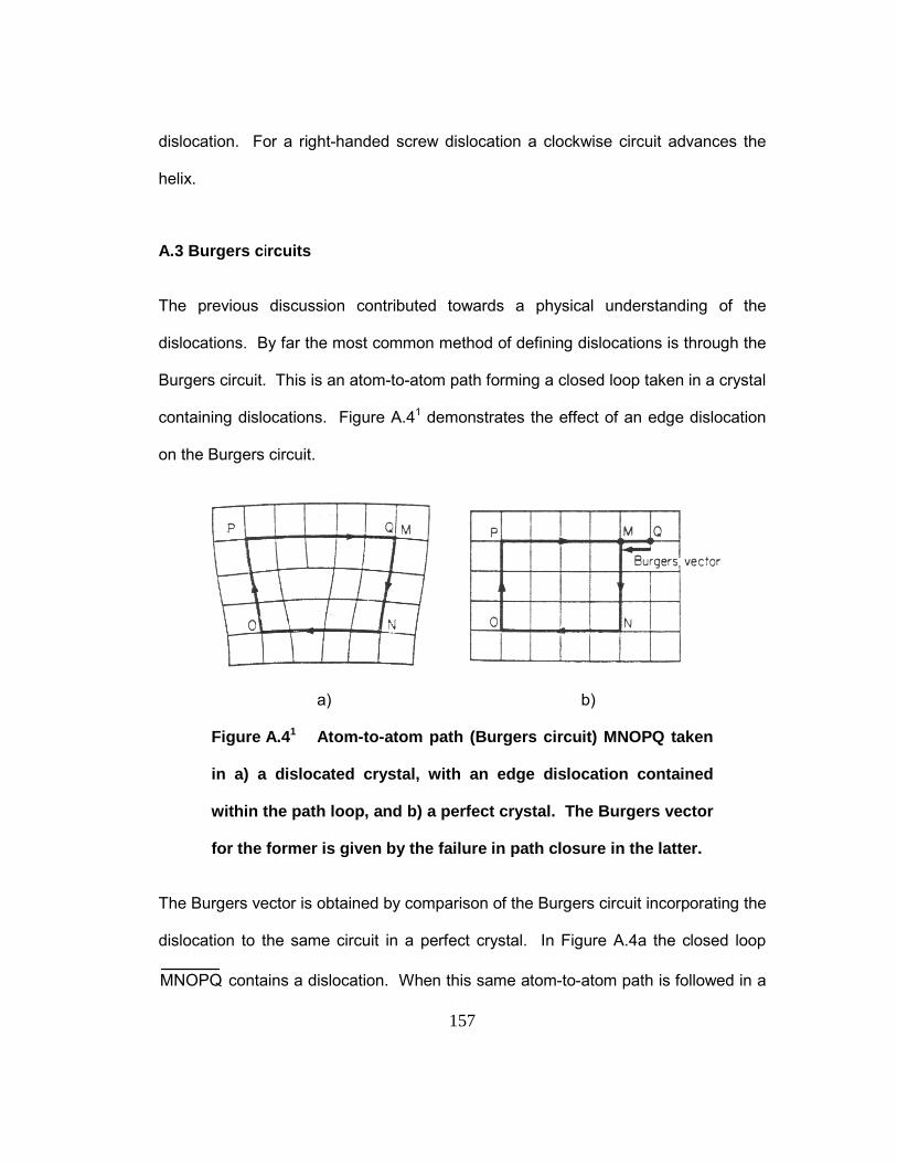
157
dislocation. For a right-handed screw dislocation a clockwise circuit advances the
helix.
A.3 Burgers circuits
The previous discussion contributed towards a physical understanding of the
dislocations. By far the most common method of defining dislocations is through the
Burgers circuit. This is an atom-to-atom path forming a closed loop taken in a crystal
containing dislocations. Figure A.41 demonstrates the effect of an edge dislocation
on the Burgers circuit.
a) b)
Figure A.41 Atom-to-atom path (Burgers circuit) MNOPQ taken
in a) a dislocated crystal, with an edge dislocation contained
within the path loop, and b) a perfect crystal. The Burgers vector
for the former is given by the failure in path closure in the latter.
The Burgers vector is obtained by comparison of the Burgers circuit incorporating the
dislocation to the same circuit in a perfect crystal. In Figure A.4a the closed loop
MNOPQ contains a dislocation. When this same atom-to-atom path is followed in a

158
perfect crystal (Figure A.4b) the circuit does not close. This will occur if and only if
the original circuit contained a dislocation. The closure failure QM is the Burgers
vector. Because it is an edge dislocation, the vector is perpendicular to the line of
the dislocation (DC in Figure A.3b). In the case of a screw dislocation, the Burgers
vector will be parallel to the line of the dislocation. For a mixed character dislocation,
the Burgers vector will be at an arbitrary angle to the dislocation line.
The dislocations discussed in the thesis are pure edge dislocations and mixed-
character dislocations. Pure screw dislocations are not known to occur in GaN or its
alloys.
1. D. Hull. Introduction to Dislocations (1965), Pergamon Press, Oxford

159
Appendix B. Processing
B.1 Activation
1.00 Solvent Clean 1.01 Soak in acetone (ultrasonic bath) for 1 minute 1.02 Soak in isopropanol (ultrasonic bath) for 1 minute1.03 Rinse in running DI water for 1 minute 1.04 Blow dry in N2 1.05 Bake; 120° oven for 5 minutes 2.00 Activate p-layer 2.01 Clean PECVD chamber (30 minute clean) 2.02 Load wafer in evaporation chamber 2.03 Evaporate 1000Å SiO2 2.04 Anneal in RTA (950°C, 3 minutes, N2 atmosphere)2.05 Soak in BHF for 5 minutes 2.06 Rinse in running DI for 1 minute 2.07 Blow dry in N2
B.2 Ohmic p-contacts
1.00 Solvent Clean 1.01 Soak in acetone (ultrasonic bath) for 1 minute 1.02 Soak in isopropanol (ultrasonic bath) for 1 minute1.03 Rinse in running DI water for 1 minute 1.04 Blow dry in N2 1.05 Dehydration bake; 120° oven for 10 minutes 1.06 Cool samples, 2 minutes 2.00 Open Windows for p-contact (Image Reversal) 2.01 Spin HMDS; 40s@6000rpm 2.02 Softbake; 95° hotplate for 1 minute 2.03 Spin photoresist AZ5214; 40s@6000rpm 2.04 Softbake; 95° hotplate for 1 minute 2.05 Remove photoresist at edges (�edge bead�) with acetone swab 2.06 Expose with mask ([email protected]/cm2 UV light) 2.07 Image reversal bake; 110° hotplate for 1 minute 2.08 Flood expose ([email protected]/cm2 UV light) 2.09 Develop in AZ400K:DI 1:5.5, 50seconds 2.10 Rinse in running DI for 1 minute; blow dry in N2

160
2.11 Second exposure: flood expose (1 [email protected]/cm2 UV light)2.12 Develop in AZ400K:DI 1:5.5, 15s 2.13 Rinse in running DI for 1 minute; blow dry in N2 3.00 Acid Dip 3.01 Soak in HCl for 20s 3.02 Rinse in DI water for 5 minutes 3.03 Blow dry in N2 4.00 Metal Evaporation 4.01 Load wafer in electron beam evaporation chamber; pump down 4.02 Evaporate 200Å Pd @ 1-2 Å/s 4.03 Evaporate 2000Å Au @ 5-7 Å/s 5.00 Liftoff 5.01 Soak in acetone for 5 minutes 5.02 Finish acetone soak with ultrasonic dip, 10s 5.03 Rinse in isopropanol (ultrasonic bath) for 1 minute 5.04 Rinse in running DI water for 1 minute 5.05 Blow Dry in N2 5.06 Anneal in RTA (650°C, 1 minute, N2 atmosphere)
B.3 Transparent p-contact layer
For transparent contact layer: same procedure as ohmic p-contacts (B.2), but
evaporate 30Å Pd @ 0.1-0.2Å/s, with no Au (steps 4.02-4.03). No anneal in RTA
(step 5.06).
B.4 Mesa etch
1.00 Open Windows for Mesa Etch 1.01 Spin photoresist AZ4110; 40s@6000rpm [or AZ4330 if etch thickness>0.5µm] 1.02 Softbake; 95° hotplate for 1 minute 1.03 Remove photoresist at edges (�edge bead�) with acetone swab 1.04 Expose with mask ([email protected]/cm2 UV light) [or 39s if AZ4330] 1.05 Develop in AZ400K:DI 1:4, 50s [or 70s if AZ4330] 1.06 Rinse in running DI for 1 minute; blow dry in N2 1.07 Hardbake; 120° oven for 10 minutes

161
2.00 Mesa Etch 2.01 Load wafer in RIE chamber; pump down 2.02 Etch to n-GaN (200W, 5mTorr, 10sccm Cl2 → 1200Å/minute etch rate) 2.03 Soak in acetone (ultrasonic bath) for 1 minute 2.04 Soak in isopropanol (ultrasonic bath) for 1 minute 2.05 Rinse in running DI water for 1 minute 2.06 Blow dry with N2
B.5 Ohmic n-contacts
1.00 Solvent Clean 1.01 Soak in acetone (ultrasonic bath) for 1 minute 1.02 Soak in isopropanol (ultrasonic bath) for 1 minute1.03 Rinse in running DI water for 1 minute 1.04 Blow dry in N2 1.05 Bake dry @ 120 deg for 10 minutes 1.06 Cool samples, 2 minutes 2.00 Open Windows for n-contact (Image Reversal) 2.01 Spin HMDS; 40s@6000rpm 2.02 Softbake; 95° hotplate for 1 minute 2.03 Spin photoresist AZ5214; 40s@6000rpm 2.04 Softbake; 95° hotplate for 1 minute 2.05 Remove photoresist at edges (�edge bead�) with acetone swab 2.06 Expose with mask ([email protected]/cm2 UV light) 2.07 Image reversal bake; 110° hotplate for 1 minute 2.08 Flood expose ([email protected]/cm2 UV light) 2.09 Develop in AZ400K:DI 1:5.5, 50seconds 2.10 Rinse in running DI for 1 minute; blow dry in N2 3.00 Descum 3.01 Load in plasma etch chamber 3.02 Descum: 30s in O2, 300torr; 100V 4.00 Metal Evaporation 4.01 Load wafer in electron beam evaporation chamber; pump down 4.02 Evaporate 100Å Ti @ 1.5Å/s 4.03 Evaporate 2000Å Al @ 5-7Å/s 4.04 Evaporate 500Å Ni @ 1.5Å/s 4.05 Evaporate 2000Å Au @ 5-7Å/s
162
5.00 Liftoff 5.01 Soak in acetone for 5 minutes 5.02 Finish acetone soak with ultrasonic dip, 10s 5.03 Rinse in isopropanol (ultrasonic bath) for 1 minute 5.04 Rinse in running DI water for 1 minute 5.05 Blow Dry in N2
B.6 Sidewall passivation
1.00 Solvent Clean 1.01 Soak in acetone (ultrasonic bath) for 1 minute 1.02 Soak in isopropanol (ultrasonic bath) for 1 minute 1.03 Rinse in running DI water for 1 minute 1.04 Blow dry in N2 1.05 Bake; 120° oven for 5 minutes 2.00 Deposit SiO2 by PECVD 2.01 Clean PECVD chamber (30 minute clean) 2.02 Load wafer in evaporation chamber with Si blank 2.03 Evaporate 1000Å-4000Å SiO2 (as required by mesa height) 2.04 Ellipsometry of SiO2 thickness on Si blank 3.00 Long-Bake Photolithography for SiO2 Via Etch 3.01 Rinse in running DI water for 1 minute 3.02 Blow dry in N2 3.03 Dehydration bake; 120°C oven for 2 hours 3.04 Cool samples, 2 minutes 3.05 Spin HMDS; 40s@6000rpm 3.06 Softbake; 95°C hotplate for 5 minutes 3.07 Spin photoresist AZ5214; 40s@6000rpm 3.08 Softbake; 95°C hotplate for 1 minute 3.09 Softbake; 90°C oven for 2 hours 3.10 Remove photoresist at edges (�edge bead�) with acetone swab 3.11 Expose with mask ([email protected]/cm2 UV light) 3.12 Image reversal bake; 110° hotplate for 1 minute 3.13 Flood expose ([email protected]/cm2 UV light) 3.14 Develop in AZ400K:DI 1:5.5, 50seconds 3.15 Rinse in running DI for 1 minute; blow dry in N2 4.00 Descum 4.01 Load in plasma etch chamber 4.02 Descum: 30s in O2, 300torr; 100V 4.03 Hardbake; 120° oven for 10 minutes

163
5.00 SiO2 Etch 5.01 Remove SiO2 from Si test wafer using pad etch solution (recipe below); record the etch time 5.02 Remove SiO2 from samples using pad etch solution (Etch time: add 5s to time required for Si wafer)5.03 Rinse in running DI for 1 minute 5.04 Blow Dry in N2 6.00 Remove Photoresist 6.01 Soak in acetone (ultrasonic bath) for 1 min 6.02 Soak in isopropanol (ultrasonic bath) for 1 min 6.03 Rinse in running DI water for 1 minute 6.04 Blow dry with N2
B.7 Contact Pad Deposition
For contact pad deposition: same procedure as ohmic n-contact deposition (B.5), but
evaporate 3000-4000Å Au, and no Al or Ni (steps 4.03-4.05).
B.8 Pad Etch Recipe
The pad etch is an alternative SiO2 etch to BHF � it does not etch metal contacts
such as the Ti/Al/Ni/Au and Pd/Au used here.
Recipe (percentages by weight): 13.5% ammonium fluoride, 31.8% acetic acid, 4.2%
ethylene glycol, and 50.5% deionised water.