5-W Microwave Integrated Circuits (MIC) Gallium Nitride ... · 5-W Microwave Integrated Circuits...
24
5-W Microwave Integrated Circuits (MIC) Gallium Nitride (GaN) Class F Power Amplifier Operating at 2.8 GHz by Caroline W. Waiyaki ARL-TR-5342 September 2010 Approved for public release; distribution unlimited.
Transcript of 5-W Microwave Integrated Circuits (MIC) Gallium Nitride ... · 5-W Microwave Integrated Circuits...
5-W Microwave Integrated Circuits (MIC) Gallium Nitride
(GaN) Class F Power Amplifier Operating at 2.8 GHz
by Caroline W. Waiyaki
ARL-TR-5342 September 2010
Approved for public release; distribution unlimited.

NOTICES
Disclaimers The findings in this report are not to be construed as an official Department of the Army position unless so designated by other authorized documents. Citation of manufacturer’s or trade names does not constitute an official endorsement or approval of the use thereof. Destroy this report when it is no longer needed. Do not return it to the originator.
Army Research Laboratory Adelphi, MD 20783-1197
ARL-TR-5342 September 2010
5-W Microwave Integrated Circuits (MIC) Gallium Nitride (GaN) Class F Power Amplifier Operating at 2.8 GHz
Caroline W. Waiyaki
Sensors and Electron Devices Directorate, ARL Approve for public release; distribution unlimited.
ii
REPORT DOCUMENTATION PAGE Form Approved OMB No. 0704-0188
Public reporting burden for this collection of information is estimated to average 1 hour per response, including the time for reviewing instructions, searching existing data sources, gathering and maintaining the data needed, and completing and reviewing the collection information. Send comments regarding this burden estimate or any other aspect of this collection of information, including suggestions for reducing the burden, to Department of Defense, Washington Headquarters Services, Directorate for Information Operations and Reports (0704-0188), 1215 Jefferson Davis Highway, Suite 1204, Arlington, VA 22202-4302. Respondents should be aware that notwithstanding any other provision of law, no person shall be subject to any penalty for failing to comply with a collection of information if it does not display a currently valid OMB control number. PLEASE DO NOT RETURN YOUR FORM TO THE ABOVE ADDRESS.
1. REPORT DATE (DD-MM-YYYY)
September 2010 2. REPORT TYPE
Final 3. DATES COVERED (From - To)
4. TITLE AND SUBTITLE
5-W Microwave Integrated Circuits (MIC) Gallium Nitride (GaN) Class F Power Amplifier Operating at 2.8 GHz
5a. CONTRACT NUMBER
5b. GRANT NUMBER
5c. PROGRAM ELEMENT NUMBER
6. AUTHOR(S)
Caroline W. Waiyaki 5d. PROJECT NUMBER
5e. TASK NUMBER
5f. WORK UNIT NUMBER
7. PERFORMING ORGANIZATION NAME(S) AND ADDRESS(ES)
U.S. Army Research Laboratory ATTN: RDRL-SER-E 2800 Powder Mill Road Adelphi MD 20780-1197
8. PERFORMING ORGANIZATION REPORT NUMBER
ARL-TR-5342
9. SPONSORING/MONITORING AGENCY NAME(S) AND ADDRESS(ES)
10. SPONSOR/MONITOR’S ACRONYM(S)
11. SPONSOR/MONITOR'S REPORT NUMBER(S)
12. DISTRIBUTION/AVAILABILITY STATEMENT
Approved for public release; distribution unlimited.
13. SUPPLEMENTARY NOTES
14. ABSTRACT
A key component of microwave telecommunication systems is the power amplifier (PA). The design parameters of a communication system, such as link performance, power budget, and thermal design are typically driven by the power amplifier’s linearity, output power, and efficiency. These design parameters of PA are the key to ensuring an efficient system because the PA is the most power-consuming circuit in the communication system. In an effort to have students involved in this research area, the International Microwave Symposium (IMS) sponsored by IEEE Microwave Theory and Technique Society (MTT-S) has introduced a High Efficiency Power Amplifier Design Competition. In this report, we present a 2.8-GHz, 5-W, highly efficient PA based on a wide bandgap gallium nitride (GaN) high electron mobility transistor (HEMT) device (CGH 40010f from CREE). The PA design was presented at the 2010 IMS Student Design Competition and achieved the competition goal of output power greater than 5 W with a measured power added efficiency (PAE) of 61% at 2.8 GHz. 15. SUBJECT TERMS
GaN, power amplifier, class F, PAE
16. SECURITY CLASSIFICATION OF: 17. LIMITATION OF ABSTRACT
UU
18. NUMBER OF PAGES
24
19a. NAME OF RESPONSIBLE PERSON
Ed Viveiros a. REPORT
Unclassified
b. ABSTRACT
Unclassified
c. THIS PAGE
Unclassified 19b. TELEPHONE NUMBER (Include area code)
(301) 394-0930 Standard Form 298 (Rev. 8/98)
Prescribed by ANSI Std. Z39.18
iii
Contents
List of Figures iv
List of Tables iv
Acknowledgments v
1. Introduction/Background 1
2. Design Methodology 2
2.1 Device Characterization: I-V and S-parameter Measurements .......................................3
2.2 Determining Matching Network Impedances .................................................................5
2.3 PA Design........................................................................................................................6
2.4 PA Fabrication .................................................................................................................8
3. Results and Discussion 9
3.1 PA Simulated Results ......................................................................................................9
3.2 PA Measured Results ....................................................................................................10
4. Conclusions 12
5. References 14
List of Symbols, Abbreviations, and Acronyms 15
Distribition List 16
iv
List of Figures
Figure 1. I-V characteristics GaN HEMT packaged device: (a) Cree large-signal model and (b) measured data (Vgs values of –2.8 V to 0.1 V in steps of 0.1 V). ........................................3
Figure 2. Simulation setup to verify Thru line standard measurements. .........................................4
Figure 3. S-parameter results comparing the full Thru line and two half Thru measurements: (a) forward and reverse transmission in dB, (b) input and output return loss, and (c) forward and reverse transmission phase. ..............................................................................4
Figure 4. (a) De-embedding process simulation and (b) the Smith chart plot comparing de-embedded data with Cree measured data (symbol – original data; solid – de-embedded data)............................................................................................................................................5
Figure 5. Cree measured and model simulated S-parameter data in ADS (blue, symbol – measured; red, solid – model). ...................................................................................................5
Figure 6. Stability factor plot of the final PA design. ......................................................................6
Figure 7. Bias flag circuit and simulation at 3.3 GHz. ....................................................................7
Figure 8. Schematic of the final PA design in Agilent’s ADS simulator. .......................................7
Figure 9. Output spectrum plot in dBm vs. frequency (markers m2, m3, and m1 show output power in dBm at fundamental, 2nd, and 3rd harmonic frequencies, respectively). .....................8
Figure 10. The final PA design: (a) a picture of the PA design presented at the IMS conference and (b) ADS layout plot of the PA. .........................................................................8
Figure 11. Test fixture layout diagram. ...........................................................................................9
Figure 12. (a) S-parameter and (b) power simulations (Ids = 200 mA, Vds= 28 V & Freq = 3.3 GHz). ..................................................................................................................................10
Figure 13. S-parameter measurements compared to the simulated data (symbol, simulated; solid, measured; blue, S11; red, S21; and pink, S22). .............................................................10
Figure 14. Power measured plot including Pout (dBm), Gain (dB), and PAE (%) of the PA design. ......................................................................................................................................11
Figure 15. Pout and PAE vs. Ids at Vds = 13 V and 15 V and input power of 25 dBm (red, Vds = 15 V and blue, Vds = 13 V). ...........................................................................................11
Figure 16. PAE vs. Frequency at the selected bias, Ids = 700 mA and Vds = 13 V. .......................12
List of Tables
Table 1. Summary of measured results at ARL, IMS, and winning PA. .......................................13

v
Acknowledgments
I wish to acknowledge the assistance and support of the following U.S. Army Research Laboratory (ARL) employees:
• Ed Viveiros for mentorship and assistance with test setup and measurements
• John Penn for assistance with the power amplifier (PA) design process
• Russell Harris for assistance with design fabrication
• Jason Stansbury for assistance with test fixture fabrication.
I also wish to acknowledge Dr. Michel Reece of Morgan State University for mentorship and guidance throughout the whole design process.

vi
INTENTIONALLY LEFT BLANK.
1
1. Introduction/Background
Historically microwave amplifiers based on vacuum-tube technology, commonly known as traveling wave tube amplifiers (TWTA), have been widely used in space telecommunication applications due to their high power capability, good efficiency, and established flight history (1). However, they are very expensive and bulky due to the high-voltage power supplies required to operate them.
Motivated by benefits such as low supply voltage, graceful degradation, low development cost, and a wide commercial technology base, there is considerable interest in developing efficient, solid-state power amplifiers (SSPAs) as an alternative to vacuum-tube technology. A fundamental hurdle to achieving this objective, however, is the fact that solid-state devices, generally in the form of monolithic microwave integrated circuits (MMICs), produce less power and operate at lower efficiencies as compared with TWTA devices.
Two III-V technologies, namely gallium arsenide (GaAs) and gallium nitride (GaN) stand at the forefront of modern SSPA research. GaAs technology is currently being employed in SSPAs for a wide variety of applications such as radar, satellite communication, and military ground communication. This technology has demonstrated maturity at microwave frequencies for many decades (1, 2). GaN, somewhat of a newcomer to MMIC technology, has power densities higher than GaAs-based technology (2). To date, high efficiency GaN power amplifiers (PAs) have been demonstrated, exhibiting efficiencies as high as 50% with 37.5 dBm of output power with associated gain of 18.2 dB at the L-band (2). Some notable foundries, such as HRL Laboratories and Cree, have even demonstrated MMIC circuits well up to the Ka-band (3, 6, 9).
In the commercial microwave communications arena, to accommodate increased bandwidth demands, communication systems are making use of complex modulated schemes. These schemes are characterized by highly varied envelops, which require PAs to be operated at less than their peak output power, commonly referred to as the back-off condition. In this back-off condition, the efficiency of the PA is dramatically reduced, leading to shorter battery life for communication handsets as well as a need for larger heat sinks to deal with the additional dissipated power (4–6).
The figure of merit that measures how efficiently a PA converts DC power to RF power is called power added efficiency (PAE). Research to increase PAE in the back-off operating condition for a PA is ongoing and some of the ways employed to increase PAE are the use of novel classes of amplifier operation, such as class D, E, F and inverse F, as well as linearity techniques, such as envelop elimination and restoration (EER) and digital pre-distortion (4, 5). The goal behind the
2
various classes of operation is to engineer the voltage and current waveforms such that there is minimal overlapping at the drain of the transistor; hence, the power dissipated is minimized and the efficiency is increased.
In this report, a class F PA has been developed using GaN high electron mobility transistor (HEMT) device technology with a large-signal model developed by Cree. Extensive theory behind class F mode of operation has been presented in references 6–11. In the design of a conventional class F amplifier, one designs the output impedance matching network by terminating the second harmonic with a short impedance and terminating the third harmonic with an open impedance, while at the fundamental, the device is presented with optimum load to achieve the highest possible power and efficiency. The details of the PA design are explained in the subsequent sections.
2. Design Methodology
In order to participate in the 2010 International Microwave Symposium (IMS) Student Amplifier Design Competition, the PA design had to comply with the complete set of rules presented in reference 7. Highlighting the crucial design parameters set by the rules, the PA should operate at a frequency of greater than 1 GHz but less than 20 GHz, and have an output power level of at least 5 W, but less than 100 W. All amplifiers should require less than 25 dBm of input power to reach the output level required for maximum efficiency. To encourage designs at higher frequencies the measured PAE is multiplied by a frequency weighting factor having the form (GHz)1/4 such that the final PAE is given by the expression below:
PAEFinal = PAE measured * (Frequency [GHz])1/4 (1)
The steps involved in the design of the PA presented in this report are as follows:
• Device selection
• Device characterization: current-voltage (I-V) and S-parameter measurements
• Determining matching network impedances
• PA design
• PA fabrication
• PA measurements
• Device selection
3
The requirement of the minimum output power of 5 W as well as the maximum input drive of 25 dBm had a great influence in the device selection. Thus, a device with sufficient nonlinearity at this input level is required. In addition, the device needs to have good gain at higher frequencies, to take advantage of the weighted frequency factor as stated in reference 7. The Cree CGH40010 GaN transistor is a 10-W device and exhibits excellent gain and matching characteristics at frequencies up to 3.5 GHz and, therefore, was selected.
2.1 Device Characterization: I-V and S-parameter Measurements
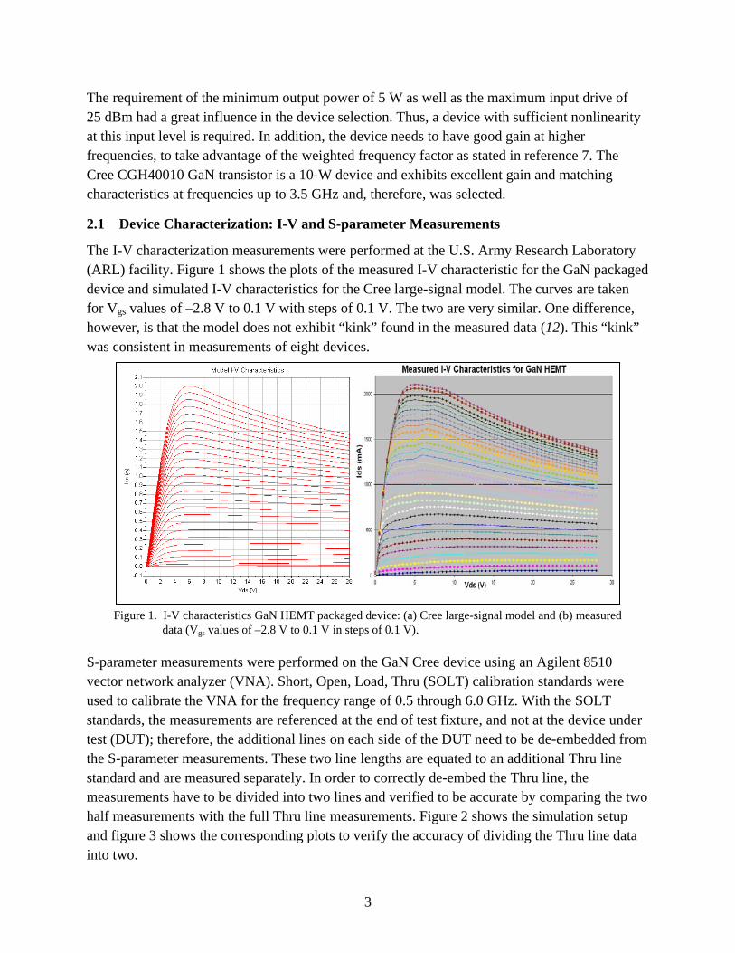
The I-V characterization measurements were performed at the U.S. Army Research Laboratory (ARL) facility. Figure 1 shows the plots of the measured I-V characteristic for the GaN packaged device and simulated I-V characteristics for the Cree large-signal model. The curves are taken for Vgs values of –2.8 V to 0.1 V with steps of 0.1 V. The two are very similar. One difference, however, is that the model does not exhibit “kink” found in the measured data (12). This “kink” was consistent in measurements of eight devices.
Figure 1. I-V characteristics GaN HEMT packaged device: (a) Cree large-signal model and (b) measured data (Vgs values of –2.8 V to 0.1 V in steps of 0.1 V).
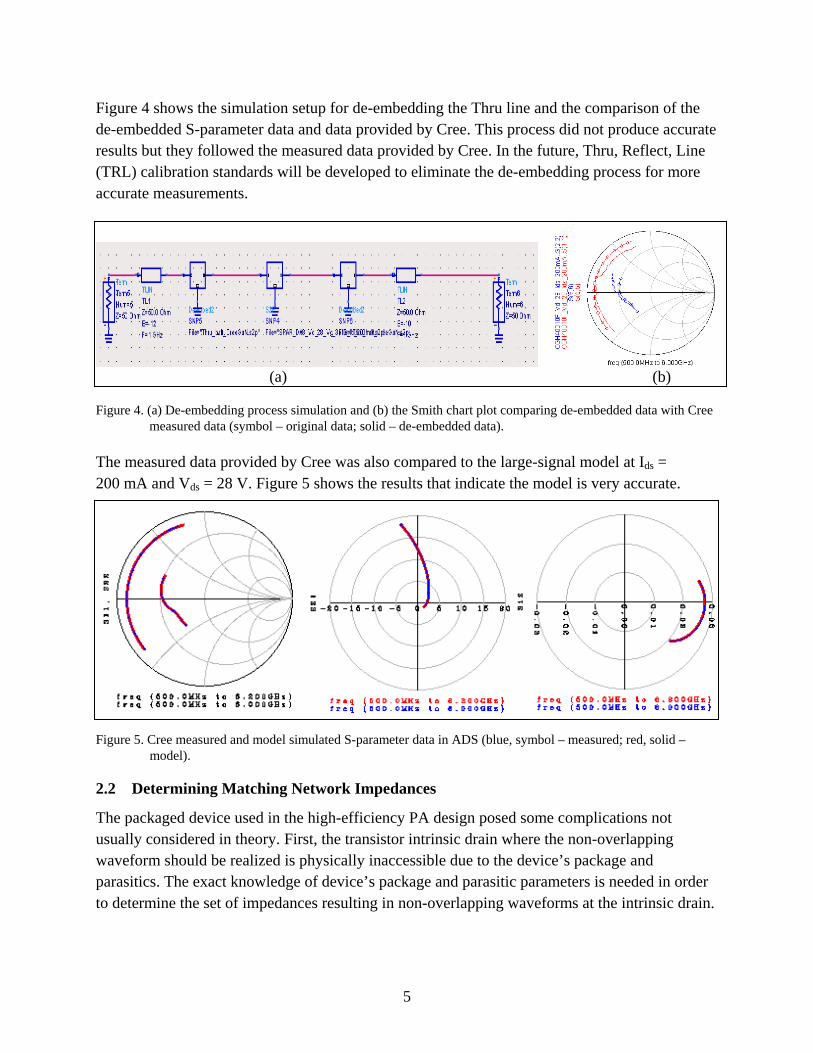
S-parameter measurements were performed on the GaN Cree device using an Agilent 8510 vector network analyzer (VNA). Short, Open, Load, Thru (SOLT) calibration standards were used to calibrate the VNA for the frequency range of 0.5 through 6.0 GHz. With the SOLT standards, the measurements are referenced at the end of test fixture, and not at the device under test (DUT); therefore, the additional lines on each side of the DUT need to be de-embedded from the S-parameter measurements. These two line lengths are equated to an additional Thru line standard and are measured separately. In order to correctly de-embed the Thru line, the measurements have to be divided into two lines and verified to be accurate by comparing the two half measurements with the full Thru line measurements. Figure 2 shows the simulation setup and figure 3 shows the corresponding plots to verify the accuracy of dividing the Thru line data into two.
4
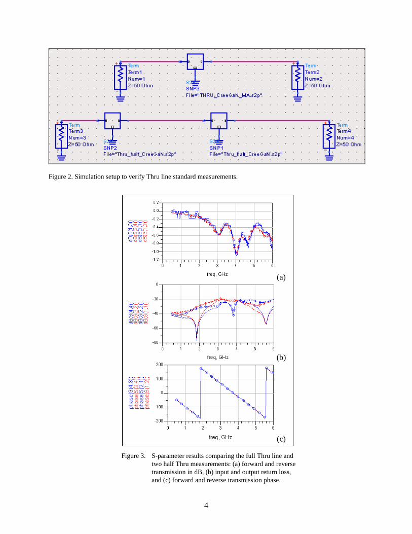
Figure 2. Simulation setup to verify Thru line standard measurements.
(a)
(b)
(c)
Figure 3. S-parameter results comparing the full Thru line and two half Thru measurements: (a) forward and reverse transmission in dB, (b) input and output return loss, and (c) forward and reverse transmission phase.
5
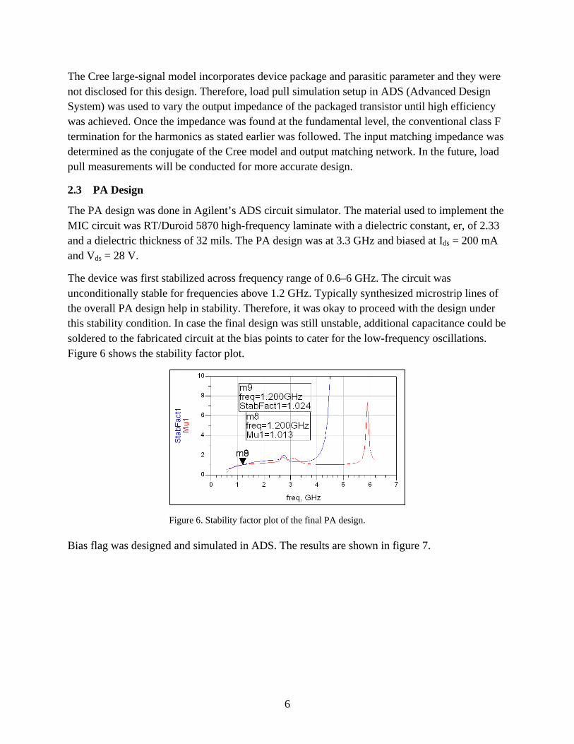
Figure 4 shows the simulation setup for de-embedding the Thru line and the comparison of the de-embedded S-parameter data and data provided by Cree. This process did not produce accurate results but they followed the measured data provided by Cree. In the future, Thru, Reflect, Line (TRL) calibration standards will be developed to eliminate the de-embedding process for more accurate measurements.
(a) (b)
Figure 4. (a) De-embedding process simulation and (b) the Smith chart plot comparing de-embedded data with Cree measured data (symbol – original data; solid – de-embedded data).
The measured data provided by Cree was also compared to the large-signal model at Ids = 200 mA and Vds = 28 V. Figure 5 shows the results that indicate the model is very accurate.
Figure 5. Cree measured and model simulated S-parameter data in ADS (blue, symbol – measured; red, solid – model).
2.2 Determining Matching Network Impedances
The packaged device used in the high-efficiency PA design posed some complications not usually considered in theory. First, the transistor intrinsic drain where the non-overlapping waveform should be realized is physically inaccessible due to the device’s package and parasitics. The exact knowledge of device’s package and parasitic parameters is needed in order to determine the set of impedances resulting in non-overlapping waveforms at the intrinsic drain.
6
The Cree large-signal model incorporates device package and parasitic parameter and they were not disclosed for this design. Therefore, load pull simulation setup in ADS (Advanced Design System) was used to vary the output impedance of the packaged transistor until high efficiency was achieved. Once the impedance was found at the fundamental level, the conventional class F termination for the harmonics as stated earlier was followed. The input matching impedance was determined as the conjugate of the Cree model and output matching network. In the future, load pull measurements will be conducted for more accurate design.
2.3 PA Design
The PA design was done in Agilent’s ADS circuit simulator. The material used to implement the MIC circuit was RT/Duroid 5870 high-frequency laminate with a dielectric constant, er, of 2.33 and a dielectric thickness of 32 mils. The PA design was at 3.3 GHz and biased at Ids = 200 mA and Vds = 28 V.
The device was first stabilized across frequency range of 0.6–6 GHz. The circuit was unconditionally stable for frequencies above 1.2 GHz. Typically synthesized microstrip lines of the overall PA design help in stability. Therefore, it was okay to proceed with the design under this stability condition. In case the final design was still unstable, additional capacitance could be soldered to the fabricated circuit at the bias points to cater for the low-frequency oscillations. Figure 6 shows the stability factor plot.
Figure 6. Stability factor plot of the final PA design.
Bias flag was designed and simulated in ADS. The results are shown in figure 7.
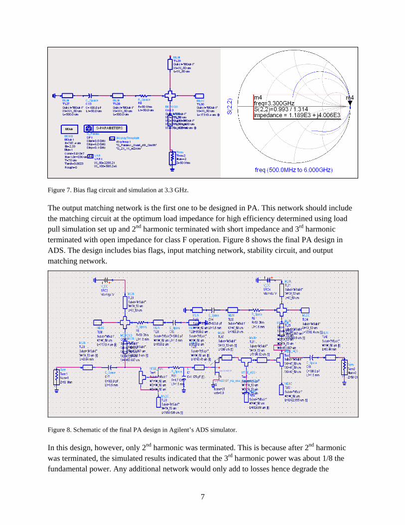
7
Figure 7. Bias flag circuit and simulation at 3.3 GHz.
The output matching network is the first one to be designed in PA. This network should include the matching circuit at the optimum load impedance for high efficiency determined using load pull simulation set up and 2nd harmonic terminated with short impedance and 3rd harmonic terminated with open impedance for class F operation. Figure 8 shows the final PA design in ADS. The design includes bias flags, input matching network, stability circuit, and output matching network.
Figure 8. Schematic of the final PA design in Agilent’s ADS simulator.
In this design, however, only 2nd harmonic was terminated. This is because after 2nd harmonic was terminated, the simulated results indicated that the 3rd harmonic power was about 1/8 the fundamental power. Any additional network would only add to losses hence degrade the
8
efficiency instead on enhancing it. Figure 9 shows the output spectrum plot confirming the previous statement. Markers m2, m3, and m1 show output power in dBm at fundamental, 2nd, and 3rd harmonic frequencies, respectively.
Figure 9. Output spectrum plot in dBm vs. frequency (markers m2, m3, and m1 show output power in dBm at fundamental, 2nd, and 3rd harmonic frequencies, respectively).
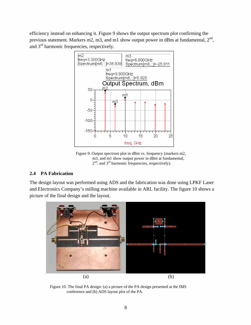
2.4 PA Fabrication
The design layout was performed using ADS and the fabrication was done using LPKF Laser and Electronics Company’s milling machine available in ARL facility. The figure 10 shows a picture of the final design and the layout.
(a) (b)
Figure 10. The final PA design: (a) a picture of the PA design presented at the IMS conference and (b) ADS layout plot of the PA.
9
A test fixture was also designed and cut at the machine shop in ARL. The test fixture layout is shown in figure 11. A slot had to be created for the packaged device to sit in with the bottom of the fixture such that it is grounded and the gate and drain leads are on top to be soldered to the MIC PA. The fixture was glued to a heat sink for dissipate power. Typically, high power amplifiers have cooling fans attached to them, but for the competition, the circuit heat sink was included with the PA design because external cooling fans were not allowed.
Figure 11. Test fixture layout diagram.
3. Results and Discussion
3.1 PA Simulated Results
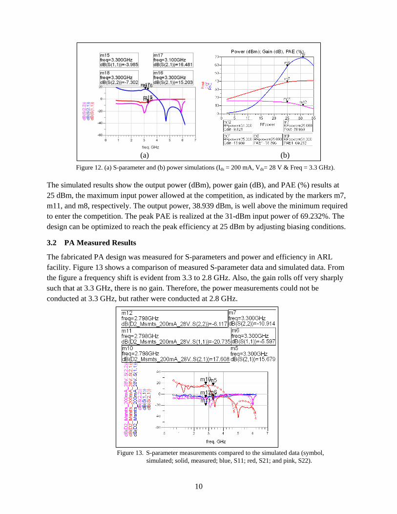
The S-parameter and power simulations at 3.3 GHz are shown in figure 12. The bias used for the simulation was Ids of 200 mA and Vds of 28 V. Small signal gain of 15.2 dB was simulated at 3.3 GHz, as shown in figure 12a. Figure 12b shows output power (dBm), power gain (dB), and PAE (%) plot simulated at the above frequency and bias point.
10
(a) (b)
Figure 12. (a) S-parameter and (b) power simulations (Ids = 200 mA, Vds= 28 V & Freq = 3.3 GHz).
The simulated results show the output power (dBm), power gain (dB), and PAE (%) results at 25 dBm, the maximum input power allowed at the competition, as indicated by the markers m7, m11, and m8, respectively. The output power, 38.939 dBm, is well above the minimum required to enter the competition. The peak PAE is realized at the 31-dBm input power of 69.232%. The design can be optimized to reach the peak efficiency at 25 dBm by adjusting biasing conditions.
3.2 PA Measured Results
The fabricated PA design was measured for S-parameters and power and efficiency in ARL facility. Figure 13 shows a comparison of measured S-parameter data and simulated data. From the figure a frequency shift is evident from 3.3 to 2.8 GHz. Also, the gain rolls off very sharply such that at 3.3 GHz, there is no gain. Therefore, the power measurements could not be conducted at 3.3 GHz, but rather were conducted at 2.8 GHz.
Figure 13. S-parameter measurements compared to the simulated data (symbol,
simulated; solid, measured; blue, S11; red, S21; and pink, S22).
11
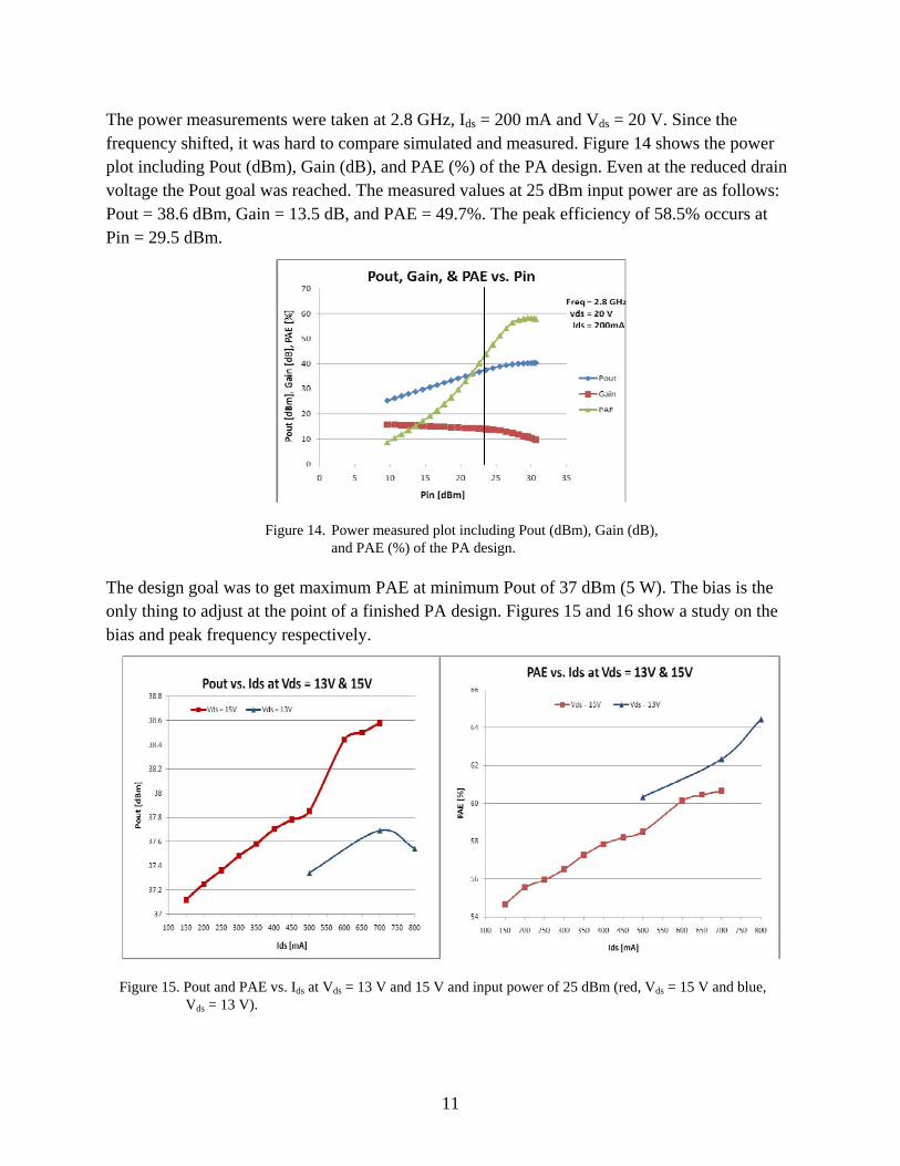
The power measurements were taken at 2.8 GHz, Ids = 200 mA and Vds = 20 V. Since the frequency shifted, it was hard to compare simulated and measured. Figure 14 shows the power plot including Pout (dBm), Gain (dB), and PAE (%) of the PA design. Even at the reduced drain voltage the Pout goal was reached. The measured values at 25 dBm input power are as follows: Pout = 38.6 dBm, Gain = 13.5 dB, and PAE = 49.7%. The peak efficiency of 58.5% occurs at Pin = 29.5 dBm.
Figure 14. Power measured plot including Pout (dBm), Gain (dB), and PAE (%) of the PA design.
The design goal was to get maximum PAE at minimum Pout of 37 dBm (5 W). The bias is the only thing to adjust at the point of a finished PA design. Figures 15 and 16 show a study on the bias and peak frequency respectively.
Figure 15. Pout and PAE vs. Ids at Vds = 13 V and 15 V and input power of 25 dBm (red, Vds = 15 V and blue, Vds = 13 V).
12
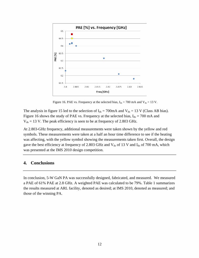
Figure 16. PAE vs. Frequency at the selected bias, Ids = 700 mA and Vds = 13 V.
The analysis in figure 15 led to the selection of Ids = 700mA and Vds = 13 V (Class AB bias). Figure 16 shows the study of PAE vs. Frequency at the selected bias, Ids = 700 mA and Vds = 13 V. The peak efficiency is seen to be at frequency of 2.803 GHz.
At 2.803-GHz frequency, additional measurements were taken shown by the yellow and red symbols. These measurements were taken at a half an hour time difference to see if the heating was affecting, with the yellow symbol showing the measurements taken first. Overall, the design gave the best efficiency at frequency of 2.803 GHz and Vds of 13 V and Ids of 700 mA, which was presented at the IMS 2010 design competition.
4. Conclusions
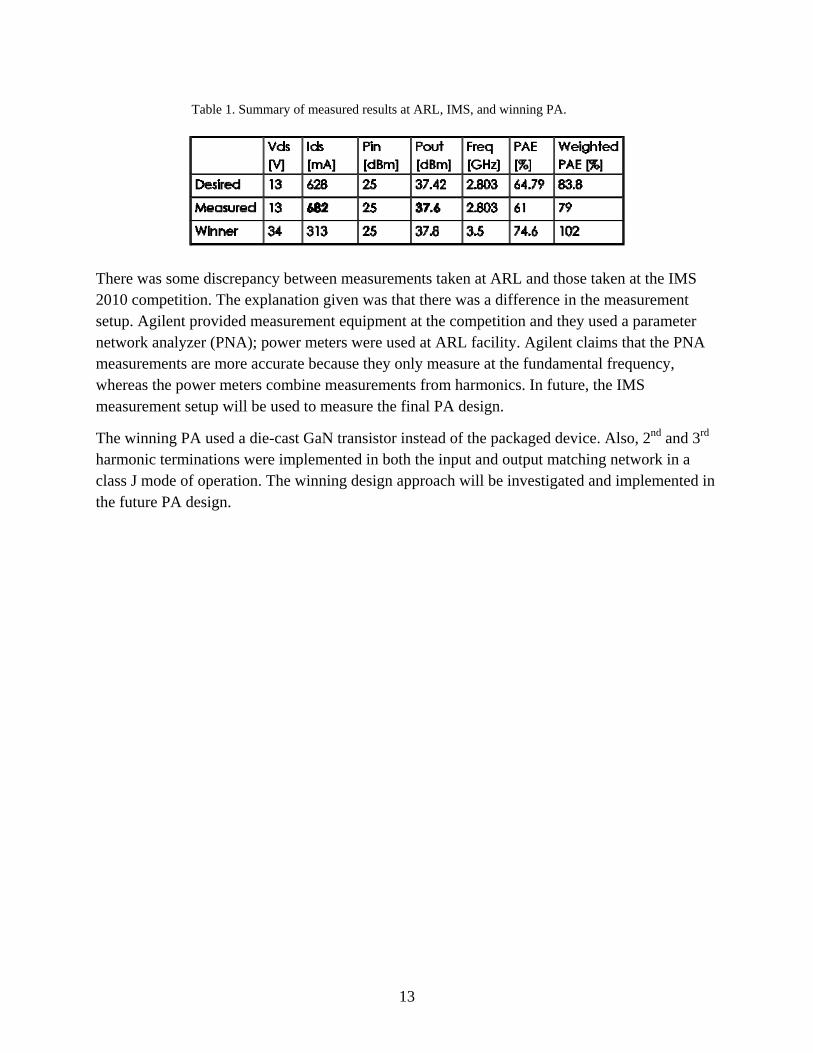
In conclusion, 5-W GaN PA was successfully designed, fabricated, and measured. We measured a PAE of 61% PAE at 2.8 GHz. A weighted PAE was calculated to be 79%. Table 1 summarizes the results measured at ARL facility, denoted as desired; at IMS 2010, denoted as measured; and those of the winning PA.
13
Table 1. Summary of measured results at ARL, IMS, and winning PA.
There was some discrepancy between measurements taken at ARL and those taken at the IMS 2010 competition. The explanation given was that there was a difference in the measurement setup. Agilent provided measurement equipment at the competition and they used a parameter network analyzer (PNA); power meters were used at ARL facility. Agilent claims that the PNA measurements are more accurate because they only measure at the fundamental frequency, whereas the power meters combine measurements from harmonics. In future, the IMS measurement setup will be used to measure the final PA design.
The winning PA used a die-cast GaN transistor instead of the packaged device. Also, 2nd and 3rd harmonic terminations were implemented in both the input and output matching network in a class J mode of operation. The winning design approach will be investigated and implemented in the future PA design.
14
5. References
1. Khan, P.; Epp, L.; Silva, A. Ka-Band Wideband Gap SSPA: General architecture considerations. IPN Progress Report, 2005.
2. Micovic, M.; et al. Ka-Band MMIC Power Amplifier in GaN HFET Technology. IEEE MTT-S Digest 2004, 1653–1656.
3. Gao, S.; Xu, H.; Heikman, S.; Mishra, U. K.; York, R. A. Two-Stage Quasi-Class-E Power Amplifier in GaN HEMT Technology. IEEE Microwave And Wireless Components Letters 2006, 16, 28–30.
4. Wu, D. Y.; Boumaiza, S. Comprehensive First-Pass Design Methodology for High Efficiency Mode Power Amplifier. IEEE Microwave Journal Feb. 2010.
5. Cripps, S. C. RF Power Amplifiers for Wireless Communications. Artech House, 1999.
6. Helaoui, M.; Ghannouch, F. M. Optimizing Losses in Distributed Multiharmonic Matching Networks Applied to the Design of an RF GaN Power Amplifier with Higher than 80% Power Added Efficiency. IEEE MTT-s 2009, 57, 314–322.
7. IMS 2010 Student Design Competition Announcement http://ims2010.org/pdf/MTT5_PA.pdf
8. Reece, M. A.; et al. A Ka-Band Class F MMIC Amplifier Design Utilizing Adaptable Knowledge-Based Neural Network Modeling Techniques. IEEE MTT-s Digest 2003, 615–618.
9. Schmelzer, D.; Long, S. I. A GaN HEMT Class F Amplifier at 2 GHz with > 80% PAE. IEEE Journal of Solid State Circuits 2007, 42, 2130–2136.
10. Khan, F. N.; Mohammadi, F. A.; Yagoub, M.C.E. A GaN HEMT Class-F Amplifier for UMTS/WCDMA Applications. IEEE International RF and Microwave Conference Proceedings, pg 478–482, 2008.
11. Rudiakova, A.; Krizhanovski, V. Maximally Flat Waveforms Operation of Class-F Power Amplifiers. Radioengineering 2001, 10, 16–19.
12. Meneghesso, G.; et al. Correlation Between Kink and Cathodoluminescence Spectra in AlGaN/GaN High Electron Mobility Transistors. Applied Physics Letters 2010, 96.
15
List of Symbols, Abbreviations, and Acronyms
ADS Advanced Design System
ARL U.S. Army Research Laboratory
DUT device under test
EER envelop elimination and restoration
GaAs gallium arsenide
GaN gallium nitride
HEMT high electron mobility transistor
IMS International Microwave Symposium
I-V current-voltage
LPKF Laser and Electronics Company
MMICs monolithic microwave integrated circuits
PA power amplifier
PAE power added efficiency
PNA parameter network analyzer
SSPAs solid-state power amplifiers
SOLT Short, Open, Load, Thru
TRL Thru, Reflect, Line
TWTA traveling wave tube amplifiers
VNA vector network analyzer
16
1 DEFENSE TECHNICAL (PDF INFORMATION CTR only) DTIC OCA 8725 JOHN J KINGMAN RD STE 0944 FORT BELVOIR VA 22060-6218 1 DIRECTOR US ARMY RESEARCH LAB IMNE ALC HRR 2800 POWDER MILL RD ADELPHI MD 20783-1197 1 DIRECTOR US ARMY RESEARCH LAB RDRL CIM L 2800 POWDER MILL RD ADELPHI MD 20783-1197 1 DIRECTOR US ARMY RESEARCH LAB RDRL CIM P 2800 POWDER MILL RD ADELPHI MD 20783-1197 1 DIRECTOR US ARMY RESEARCH LAB RDRL SER L PIEKARSKI 2800 POWDER MILL RD ADELPHI MD 20783-1197 1 CERDEC S&TCD LOUIS CORYELL RDER STC TA BUILDING 210 ROOM 215 FORT MONMOUTH, NJ 07703-5203 1 CDR USA CERDEC I2WD STEVE HAUGHT ATTN: RDER IWR CI (HAUGHT) FORT MONMOUTH NJ 07703 2 CERDEC I2WD
RDER IWR CI ROBERT GROSS (SUITE D) HERALD BELJOUR (SUITE A)
6240 GUARDIAN GATEWAY APG MD 21005 ABERDEEN PROVING GROUND 1 DIR USARL RDRL CIM G (BLDG 4600)