Y DIODES ON GaN (GALLIUM NITRIDE) SEMICONDUCTORS …
111
Y DIODES ON GaN (GALLIUM NITRIDE) SEMICONDUCTORS SCHOTTK' by VEENA VIJAYAN, B.Tech. A THESIS IN ELECTRICAL ENGINEERING Submitted to the Graduate Faculty of Texas Tech University in Partial Fulfillment of the Requirements for the Degree of MASTER OF SCIENCE IN ELECTRICAL ENGINEERING Approved Chairperson of the Committee Accepted "bean of tl^ Graduate Scho^ August, 2000
Transcript of Y DIODES ON GaN (GALLIUM NITRIDE) SEMICONDUCTORS …
Y DIODES ON GaN (GALLIUM NITRIDE) SEMICONDUCTORS SCHOTTK'
by
VEENA VIJAYAN, B.Tech.
A THESIS
IN
ELECTRICAL ENGINEERING
Submitted to the Graduate Faculty of Texas Tech University in
Partial Fulfillment of the Requirements for
the Degree of
MASTER OF SCIENCE
IN
ELECTRICAL ENGINEERING
Approved
Chairperson of the Committee
Accepted
"bean of t l ^ Graduate Scho^
August, 2000

ACKNOWLEDGEMENTS
I would like to express my sincere gratitude to everyone who assisted me during
this research work. As a firm believer in God, I would first thank him for giving me
support through all these years.
I would first like to thank Dr. Henryk Temkin, advisor and Jack Maddox
Distinguished Engineering Chair, for giving me an opportunity to work with highly
skilled scientists in a world-class laboratory. I am thankful for having benefited from his
confidence and was able to contribute to a major research project. The project done under
his guidance has enriched me with some priceless experiences, which I will cherish
forever.
I would like to thank Dr. Jon Bredeson and Dr. Tim Dallas for serving as my
committee members and spending their valuable time in reviewing this thesis.
I would like to thank my colleagues Sergey Nikisin, Caixia Jin, Vladimir
Kuryatkov and Marvin Cummings for valuable hours of discussions.
I would like to thank my parents and my siblings Vini and Vijesh for their support
and patience since I left home. Finally, I would like to express my gratitude to Shahin, for
his love and support.
11
TABLE OF CONTENTS
ACKNOWLEDMENTS ii
ABSTRACT vi
LIST OF TABLES vii
LIST OF FIGURES viii
CHAPTER
L INTRODUCTION 1
1.1 Thesis Overview 2
1.2 Why GaN? 3
1.3 An Introduction to Gallium Nitride 4
1.4 Properties of Gallium Nitride 5
1.5 Application and Future of Gallium Nitride 9
IL METAL SEMICONDUCTOR CONTACTS 12
2.1 Introduction 12
2.2 Schottky Barriers 13
2.3 Ohmic Contacts 20
2.4 High-Quality Schottky Diodes 22
2.5 Applications of Schottky Diodes 22
2.6 Other Work 23
m. CHARACTERIZATION 27
3.1 Semiconductor Device Characterization Technique 27
3.2 Capacitance-Voltage Measurements 30
iii

3.3 I-V Characteristics 36
IV. EXPERIMETAL PROCEDURE USED FOR
THE FABRICATION OF SCHOTTKY DIODES 39
4.1 Structure and Growth of the GaN Sample Used 39
4.2 Masks Used for the Fabrication Process 41
4.3 Fabrication Procedure of the Schottky Diodes 45
4.4 Selection of the Type of Photoresist Material 45
4.5 Photoresist Processing Technique 46
4.6 Choice of the Metals Used for Making the Ohmic
and Schottky Contacts 51
4.7 Deposition Technology 52
4.8 The Evaporation System Used for the Experiment 52
4.9 Liff-Off Technique 61
4.10 Other Work Involving Different Device Geomentries 61
V. INVESTIGATION OF RESULTS AND DISCUSSION 64
5.1 Experiment 64
5.2 Results and Discussion of Capacitance-Voltage Measurements using One-Mask Process 67
5.3 Results and Discussion of Current-Voltage Measurements using One-Mask Process 74
5.4 Results and Discussion of Capacitance-Voltage Measurements using Two-Mask Process 81
5.5 Results and Discussion of Current-Voltage Measurements using Two-Mask Process 88
IV

5.6 Conclusion 94
VI. CONCLUSIONS 95
REFERENCES 96
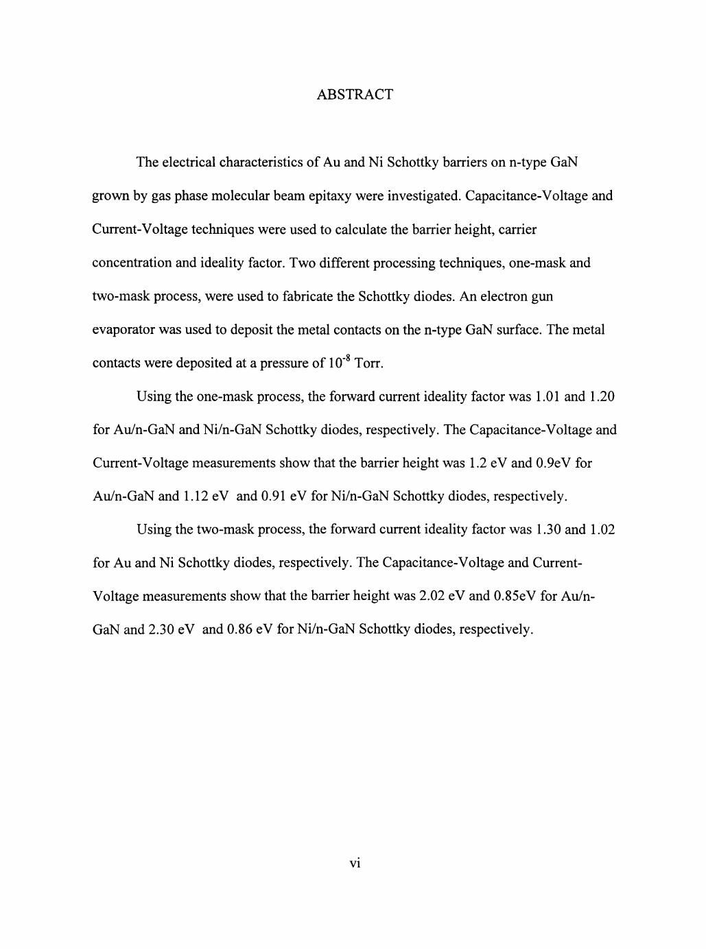
ABSTRACT
The electrical characteristics of Au and Ni Schottky barriers on n-type GaN
grown by gas phase molecular beam epitaxy were investigated. Capacitance-Voltage and
Current-Voltage techniques were used to calculate the barrier height, carrier
concentration and ideality factor. Two different processing techniques, one-mask and
two-mask process, were used to fabricate the Schottky diodes. An electron gun
evaporator was used to deposit the metal contacts on the n-type GaN surface. The metal
o
contacts were deposited at a pressure of 10" Torr.
Using the one-mask process, the forward current ideality factor was 1.01 and 1.20
for Au/n-GaN and Ni/n-GaN Schottky diodes, respectively. The Capacitance-Voltage and
Current-Voltage measurements show that the barrier height was 1.2 eV and 0.9eV for
Au/n-GaN and 1.12 eV and 0.91 eV for Ni/n-GaN Schottky diodes, respectively.
Using the two-mask process, the forward current ideality factor was 1.30 and 1.02
for Au and Ni Schottky diodes, respectively. The Capacitance-Voltage and Current-
Voltage measurements show that the barrier height was 2.02 eV and 0.85eV for Au/n-
GaN and 2.30 eV and 0.86 eV for Ni/n-GaN Schottky diodes, respectively.
VI
LIST OF TABLES
2.1 Work function of some metals 15
2.2 Electron affinity of some semiconductors 15
2.3 Electrical nature of Ideal MS contacts 20
2.4 Report on ohmic contacts on n-GaN by different research groups 26
4.1 Dimensions of the crucible liner 56
5.1 Summary of C-V measurements on Au/n-GaN using one-mask process 73
5.2 Summary of C-V measurements on Ni/n-GaN using one-mask process 73
5.3 Summary of characteristics of Schottky barriers from I-V
measurements using one-mask 79
5.4 Summary of C-V measurements on Au/n-GaN using two-mask process 85
5.5 Summary of C-V measurements on Au/n-GaN using two-mask process 85
5.6 Summary of C-V measurements on Ni/n-GaN using two-mask process 86
5.7 Summary of characteristics of Schottky barriers from I-V measurements using the two-mask process 93
Vll

LIST OF FIGURES
1.1 Wurtzite Structure 6
1.2 Rocksalt Structure 7
1.3 Zinc Blende Structure 8
2.1 Energy band diagram for a metal and a n-type semiconductor 13
2.2 Energy band diagram for Schottky contact after contact formation 15
2.3 Energy band diagram for a metal and n-type semiconductor
with an interfacial layer between them 16
2.4 Response of bias voltage to a Schottky diode 18
2.5 Energy band diagram for an ohmic contact after contact formation 21
2.6 I-V curve for the ohmic contact structure 21
2.7 Reported Schottky barrier heights versus Metal work function of metals 23
3.1 Band diagram of Schottky barrier in reverse bias 30
3.2 Charge density due to mobile carriers 32
4.1 Cross-sectional structure of the sample used in the experiment 40
4.2 Top view of the diode configuration used in one-mask process 42
4.3 Cross-sectional view of the diode structure in one-mask process 42
4.4 Top view of the ohmic contact configuration used in two-mask process 43
4.5 Cross-sectional view of the ohmic contact structure in two-mask process 43
4.6 Top view of the Schottky contact configuration used in two-mask process 44
4.7 Cross-sectional view of the diode structure in two-mask process 44
Vlll

4.8 Flow chart of the fabrication procedure of Schottky diodes 45
4.9 Flow chart of the resist process 46
4.10 Major methods of exposure technique 50
4.11 The evaporator system 54
4.12 Crucible Liner 56
4.13 Evaporation Chamber 58
4.14 Control Cabinet 59
4.15 Schematic of mesa diode 62
4.16 Schematic of metal field plate device 62
4.17 Schematic of a Schottky diode 63
5.1 C-V measurements of Au/n-GaN using one-mask for different frequencies 68
5.2 1 /C^ versus V graph of Au/n-GaN Schottky diodes at different frequencies 69
5.3 C-V measurements of Ni/n-GaN using one-mask for different frequencies 70
5.4 1/C^ versus V graph of Ni/n-GaN Schottky diodes at different frequencies 71
5.5 Forward I-V characteristics of one-mask Au/n-GaN diodes 75
5.6 Forward I-V characteristics of one-mask Ni/n-GaN diodes 76
5.7 Reverse I-V characteristics of one-mask Au/n-GaN diodes 77
5.8 Reverse I-V characteristics of one-mask Ni/n-GaN diodes 78
5.9 C-V measurements of Au/n-GaN using two-mask for different } ft '\
frequencies. The carrier concentration was approximately 10 cm" 82
5.10 C-V measurements of Au/n-GaN using two-mask for different 17 '
frequencies. The carrier concentration was approximately 10 cm" 83
IX
5.11 C-V measurements of Ni/n-GaN using two-mask for different frequencies. The carrier concentration was approximately 10 cm' 84
5.12 Forward I-V characteristics of Au/n-GaN Schottky diodes using two-mask process 89
5.13 Forward I-V characteristics of Ni/n-GaN Schottky diodes using Two-mask process 90
5.14 Reverse I-V characteristics of Au/n-GaN Schottky diodes using two-mask process 91
5.15 Reverse I-V characteristics of Au/n-GaN Schottky diodes using two-mask process 92
CHAPTER I
INTRODUCTION
Even though ni-V group nitride compounds like gallium nitride were studied for
a long time, only recently have they changed from materials of research interest to
commercially important semiconductors. The ability to produce conducting p-type GaN
and improvements in the growth of high quality epitaxial layers on GaN helped in the
fabrication of commercially viable devices. GaN technology is progressing so rapidly that
the impact made on the electronic device front suggests that III-V nitride will play an
important role in the fiiture development of high-power, high-frequency, and high-
temperature electronic devices. III-V nitride device development has emphasized field-
effect transistor (FET) structures. This is due to the fact that FETs play an important role
in many electronic device applications and moreover, the GaN based FETs have recently
shown excellent microwave high power and high temperature performance.
However, in order to realize the potential of these materials for high temperature
applications, high quality thermally stable contacts, which do not deteriorate under high
temperature operation on GaN based materials, are required. Good Schottky contacts and
low resistance ohmic contact are a prerequisite for the high performance FETs. Placing a
metal in contact with a wide bandgap III-V semiconductor such as GaN generally results
in a rectifying contact rather then an ohmic one. Achieving a good Schottky contact and a
stable, low-resistance ohmic contact has been as much technical art as science. Thus, it is
important to investigate which metals are appropriate for use as gate metals in GaN based
field effect transistors.

In this thesis, I present the investigations of Au and Ni Schottky diode
characteristics on n-GaN using different ways of fabrication procedures. The
capacitance-voltage (C-V) and current-voltage (I-V) characteristics of the barriers were
investigated. Various parameters like carrier concentration and barrier height were
determined. Barrier height was determined using both C-V and I-V characteristics.
1.1 Thesis Overview
The work described in this thesis is the fabrication of Schottky diodes on n-
Gallium Nitride semiconductor sample using different fabrication techniques. I will also
characterize and compare Au and Ni Schottky diodes.
Chapter I describes Gallium Nitride semiconductor, its properties, and
applications and gives a perspective on the current and fiiture evolution of this exciting
field. It includes the importance of GaN FETs, blue LEDs, and laser diodes.
Chapter II discusses the theory and operation of metal-semiconductor contacts. It
deals with the definition of high-quality Schottky diodes, covers the application of these
diodes, and compares other work done by other groups.
Chapter III deals with the various characterization techniques used. It covers the
theory of C-V and I-V analysis and the derivation of different parameters and equipment
used for these measurements.
Chapter IV deals with the structure of the Schottky diodes which includes the
structure of the sample, the masks used in the process techniques, the fabrication
procedure of the diodes, the choice of the metal used, the experimental set-up used to
make the contacts.
Chapter V deals with the results obtained and the correction made to the data to
avoid the influence of series resistance.
Chapter VI is the summary of the thesis.
1.2 WhvGaN?
The main reason behind all current GaN research is that GaN based devices can:
(1) operate at high temperatures conditions, and (2) the GaN based devices can deliver
more power than current, commercially-available devices.
GaN has broad commercial applications in blue/ultraviolet optoelectronic devices
such as light-emitting diodes and laser diodes. The blue LEDs are of dual importance:
they can be used as emitters where strong, energy-efficient and reliable green, blue, and
ultraviolet light sources are required. Apart from this they enable the production of fiill
color LED displays by complementing the color spectrum of available LEDs. ^
Another attractive property of GaN semiconductor is its wide bandgap. The
intrinsic carrier concentration of any material at any temperature decreases exponentially
with bandgap, which implies that wide bandgap materials like GaN go intrinsic at much
higher temperatures than other semiconductor materials like Si, Ge, or GaAs. This makes
GaN attractive for high temperature applications. The usual limitation of a power
transistor is heating due to various internal losses. This is the reason that Si power
transistors are enhanced with air-cooling fins or water cooling additions. A GaN power
transistor can operate at high temperatures due to internal dissipations without cooling.
GaN semiconductor has high breakdown fields. High power operation is a direct
result of high breakdown. The breakdown field of GaN is about 3x10^ V/cm, as
compared to 2 and 4x10^ V/cm for Si and GaAs, "* respectively.
The ni-V nitride material system supports the heterostructure technology. Various
devices using GaN/AlGaN heterojunctions can be made. Quantum wells, modulation-
doped FET's, and heterojunction bipolar transistors can all be made in this system, giving
access to new spectral regions for optical devices and new operating regimes for
electronic devices.
The scientific and technological interest in Gallium Nitride has exploded in the
past few years, leading some to predict that GaN will eventually become the third most
important semiconductor behind GaAs and Si.
1.3 An Introduction to Gallium Nitride
Gallium Nitride was synthesized in 1932 by Johnson et al. ^ and by Juza and
Hahn ^ in 1938 by passing ammonia over hot gallium to investigate the crystal structure
and lattice constants of GaN as part of a systematic study of some compounds. The same
method was used by Grimmeiss et al. ^ and small crystals of GaN was produced in 1959.
GaN was first synthesized in the epitaxial form on a sapphire substrate by hydride vapor-
phase epitaxy by Maruska and Tienjen. ^ In the beginning, all GaN made was very
conducting n-type even when not deliberately doped. The donors were beHeved to be
nitrogen vacancies.
The availability of large area samples * and the improvement in the growth of
good quality GaN epilayers ^ gave momentum to the GaN research. The first blue GaN
LED was fabricated by Pankove et al.'* '' * The other important discoveries made at that
period includes study of negative electron affinity, ^^ surface acoustic wave
generation, ^ ' and solar blind UV detectors. ^ ^ Yoshida et al. ' used AIN buffer layers to
improve the quality of the epilayers and Amano et al.' "* obtained p-type conductivity in
GaN samples.
By the mid 1990s, there was rapid progress in the fabricating devices from GaN.
Akasaki and co-workers'* " ' ^ made the first p-n junction GaN LED. Nakamura and co
workers fabricated the blue and green LEDs. ' ^ - ^1 Akasaki and collaborators ^ ^
demonstrated the injection lasers in 1995. Currently, significant progress is made in
generating transistors based on GaN, that promise to deliver up to a hundred times as
much power at microwave frequencies.
1.4 Properties of Gallium Nitride
1.4.1 Crystal Structure of Gallium Nitride
GaN and its related compounds (AIN, InN, BN) can crystallize in any of the
following three crystal structures:
1. Wurtzite,
2. Zinc-blende,
3. Rock-salt.
Crystallographically, the Zinc-blende structure and Wurtzite structures are very
closely related. At ambient conditions, the thermodynamically stable structures are
Wurzite for GaN, AIM, and InN and Zinc-blende for BN. Zinc-blende structure is

metastable and has been stabilized by heteroepitaxial growth of thin films on substrates
such as silicon. A phase transition to rock-salt structure takes place at high pressure.
The phase grouping for Wurtzite structure is P6 3mc. The wurtzite structure has a
hexagonal unit cell and thus has two lattice constants a and c. It consists of two
interpenetrating hexagonal close-packed (hep) sublattices offset along the c axis by u=3/8
as shown in Figure 1.1. In the Wurtzite structure every atom of one type is surrounded by
four atoms of the other type which are arranged at the edges of a tetrahedron. Each
lattice is different from the ideal geomentry due to the deviations of axial ratios from the
ideal values for hexagonal close packing of spheres and therefore there are two bond
lengths defined by Yeh et al. (1992):
R(l)=u.candR(2)=a*[l/3 + ( l /2 -w)*(c /a )^ ]^^^
Where u is called dimensionless cell internal structure parameter. For an ideal wurtzite
structure R(l) is equal to R(2).
GaorN
O NorGa
Figure 1.1 Wurtzite Structure.

The space grouping for rock-salt structure is Fm3m. In this structure each atom
has six nearest neighbors located at the comers of an octahedron. The structure consists
of two interpenetrating face centered cubic sublattices each with one t5^e of atom, i.e.,
the anions from a face centered cubic (fee) lattice where open sites in between are
occupied by ions of opposite charge. The opposite charge in turn build an fee lattice
offset along the cubic edge by half a unit cell as shown in the Figure 1.2.
Figure 1.2 Rocksalt structure.
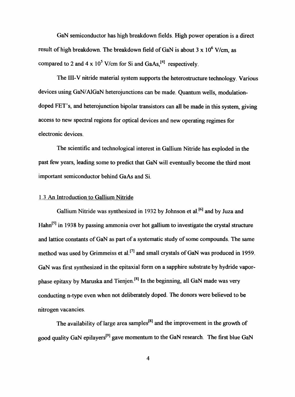
The space grouping for Zinc-blende structure is F4m3. In Zinc-blende structure
each atom of one type is surrounded by four atoms of the other type, forming a regular
tetrahedron. The structure consists of two interpenetrating face-centered cubic sublattices
offset by one quarter of the distance along a body diagonal as shown in the Figure 1.3.
There are four molecules per unit cell, the coordinates of one atom type being (0,0,0),
(0,1/2,1/2), (1/2,0, l/2),(l/2,1/2,0) and those of other being (l/4,l/4,l/4),(l/4,3/4,3/4),
(3/4,1/4,3/4), (3/4,3/4,1/4)
Figure 1.3 Zinc blende structure
1.4.2 Chemical properties of GaN
GaN is an exceedingly stable compound and exhibits significant hardness, which
makes it an attractive material for protective coating. Moreover, owing due to its wide
energy bandgap of 3.4 evV, GaN can be used for violet, blue and green light emitting
diodes and is an excellent material for high temperature device applications. Various
studies have reported that GaN is insoluble in water, acids or bases at room temperature
but does dissolve in a hot alkali solution at a very slow rate. ^
8
1.4.3 Negative Electron Affmity (NEA)
GaN has a negative electron affinity, a condition that allows electrons in the
conduction band to escape into the vacuum. This property makes these materials useful
for photodetectors and including displays.
1.4.4 Pyroelectricity
GaN has a large pyroelectric constant approximately equal to 10"* V/k. This makes
it a good candidate for piezoelectric elements and sensors. ^
1.5 Application and Future of GaN
GaN has been the subject of intensive research for past few years. The world
wide market for devices employing GaN semiconductor is expected to exceed
$3 billion by 2006.
GaN compounds show much promise for both optoelectronic and electronic
appHcations. The bandgap (3.26-3.45) enables GaN to be an efficient optoelectronic
technology. The high saturation drift velocity and high breakdown electric fields enable
high frequency operation at high electric fileds and in high-temperature conditions. Some
of the appHcations of GaN technology are listed below.
1.5.1 Electronics
The large bandgap of GaN make it suitable for high-temperatue applications such
as FETs with potential applications at high temperature can be fabricated using GaN. The
first GaN FET was reported in 1993.'^^' The device fabricated had many desu-able
features such as high pinch-off, reasonable transconductance, and high vohage operation.
1.5.2 Blue Light Emitting Diodes
Major developments in the wide gap III-V nitride semiconductors have led to the
commercial production of high-power UV/blue/green light-emitting diodes. Previously,
full-color LED displays were not possible because they were too weak and did not cover
the necessary color spectrum.
1.5.3 GaN UV Injection Lasers
GaN lasers have the potential to take a large fraction of the market for the optical
reading and writing of data in compact disk memories and opto-magnetic memories.
Since the storage density is inversely proportional to the square of wavelength, a 360 nm
laser would allow a factor of five increase in the information storage in compact discs.
GaN based laser diodes can also be used in projection displays.
1.5.4 UV Detectors
GaN constitutes an ideal material for photodetectors that do not respond to visible
light, i.e., solar-blind UV detectors. This makes it of interest for use in space applications.
10

1.5.5 X-Ray Detectors
GaN can also be used as an X-Ray detector. GaN p-n junctions are sensitive to X-
rays because X rays are energetic enough to generate electron-hole pairs that are then
separated by the internal field of the p-n junction to produce a photo-voltage.' ^^
1.5.6 Space AppHcations
For space applications radiation-hard materials are needed. GaN can be used as a
radiation hard window material on top of a solar cell.
1.5.7 Bipolar Transistors
GaN technology also supports bipolar devices like heterojunction bipolar
transistors (HBTs) for the fabrication of high performance microwave devices.
AlGaN/GaN based heterostructure field effect transistors have been reported to have
good transconductance and saturation current.
II
CHAPTER n
METAL SEMICONDUCTOR CONTACTS
2.1 Introduction
The metal-semiconductor contact forms an important link between the
semiconductor and the outside world. The quality of metal-semiconductor (MS) contact
is critical to the performance of various semiconductor devices and integrated circuits and
therefore plays a very important role in all solid state devices.
An ideal MS contact has the following properties: (1) The metal and
semiconductor are assumed to be in intimate contact, i.e., no interfacial layer is present
between the components. (2) There are no intermixing of the metal and semiconductor.
(3) There are no surface charges at the metal semiconductor interface.' ^
Two types of metal-semiconductor contacts are encountered in the fabrication of
semiconductor devices. They are
• Schottky or (rectifying contacts),
• Ohmic or (non-rectifying contacts).
A Schottky barrier contact or the rectifying MS contact is an important device and
is found in a number of device structures. A Schottky barrier contact shows an
asymmetrical current-voltage (I-V) characteristic when the bias of the externally applied
voltage to the contact is changed. Where as the ohmic or non-rectifying contact shows
linear I-V characteristics regardless of the polarity of the bias voltage applied.
12

2.2 Schottky Barriers
The Schottky contact is an important element in many GaN devices. It is
important for studying the electrical properties of a semiconductor material. The Schottky
barrier is also used to study the bulk defects and interface properties of a metal-
semiconductor system. For the performance of FETs the size and placement of the gate is
a critical factor. The physics involved in metal-semiconductor contact is described in this
section.
The energy band diagrams for a metal and a n-type semiconductor material are
shown in Figure 2.1. Both the metal and the semiconductor are electrically isolated from
each other.
Metal Eo Eo n-type Semiconductor
"X" X \
EFS
Figure 2.1 Energy band diagram for a metal and a n-type semiconductor.
13

In Figure 2.1, the cross-hatching signifies allowed states that are almost
completely filled with electrons, whereas the vertical line represents the surface.
The horizontal line at the top is called the vacuum level, Eo, which denotes the
minimum energy an electron must possess to completely free itself from the surface of
the material. The metal workfimction, ^M, is defined as the minimum energy required to
raise an electron from the metal surface into free space. Each metal has a constant metal
workfimction. The work functions of various metals are given in Table 2.1. The
workfimction (Os) of a semiconductor material is the energy difference between the
vacuum level and the Fermi energy level. The semiconductor workfimction, Os, is
composed of two distinct parts; ^ ^ that is
^S = X + ( E C - E F ) F B
Where x is the electron affmity, and is given by x = (Eo - Ec)| surface.
The electron affinities of several semiconductors are shown in Table 2.2.
Figure 2.2 shows energy band diagrams for a metal and n-type semiconductor
system after contact formation. The workfimction of the semiconductor is less than that
of the metal, i.e., ^u > (t>s which is the necessary condition for the formation of Schottky
barriers between a metal and a n-type semiconductor. Figure 2.2(a) shows the condition
when the metal comes into contact with the semiconductor. Since the Fremi level of the
semiconductor is above that of the metal, the system is not in equilibrium. For the system
to be under equilibrium, the Fermi energy level must be invariant with position
throughout the structure. Consequentiy, a short time after the contact formation, electrons
from the semiconductor will flow into the lower energy states in the metal. The net loss
14
Table 2.1 Work Function of some Metals
Element
Ag, Silver
Al, Aluminium
Au, Gold
Cr, Chromium
Mo,Molybdenum
Ni, Nickel
Pd, Palladium
Pt, Platium
Ti, Titanium
W, Tungsten
Work Function,(|)m (eV)
4.26
4.28
5.1
4.5
4.6
5.15
5.12
5.65
4.33
4.55
Table 2.2 Electron affinity of some semiconductors
Element
Ge, Germanium
Si, Silicon
GaAs, Gallium Arsenide
GaN, Gallium Nitride
Electron Affinity,x (eV)
4.13
4.01
4.07
4.01
15
of electrons from the semiconductor creates a surface depletion region and as a result the
potential barrier seen by the electron, from the semiconductor to the metal increases. This
phenomenon will continue until the Fermi level Epis the same through out the structure.
The net equilibrium band diagram for an ideal ^u > <t)s metal to n-type semiconductor
contact is shown in the Figure 2.2(b).
n-type semiconductor
-FM
(a)
(b)
Figure 2.2 Energy band diagram for Schottky contact after contact formation.
16
The barrier height for an ideal metal-semiconductor Schottky contact is equal to
the difference between the work flmction of a metal OM and the electron affmity xs of a
semiconductor. In other words it is the potential barrier seen by the electrons in the metal
trying to move to the semiconductor. For a metal/n-type semiconductor Schottky contact
this is given by
(|)Bn - (|)M - Xs ideal MS(n-type contact).
The barrier seen by the electrons in the conduction band trying to move into the
metal is known as the built-in potential and is denoted by Vbi and is given by
V b i = <l>Bn - 4)n-
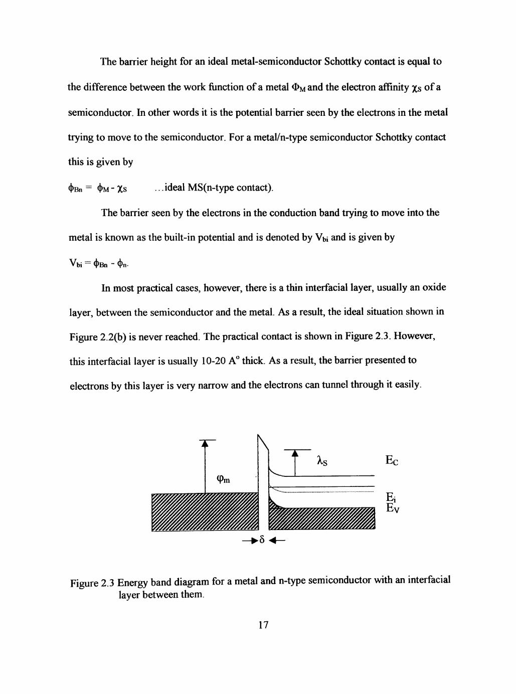
In most practical cases, however, there is a thin interfacial layer, usually an oxide
layer, between the semiconductor and the metal. As a result, the ideal situation shown in
Figure 2.2(b) is never reached. The practical contact is shown in Figure 2.3. However,
this interfacial layer is usually 10-20 A° thick. As a result, the barrier presented to
electrons by this layer is very narrow and the electrons can tunnel through it easily.
(pm
N
Ei Ev
Figure 2.3 Energy band diagram for a metal and n-type semiconductor with an interfacial layer between them.
17
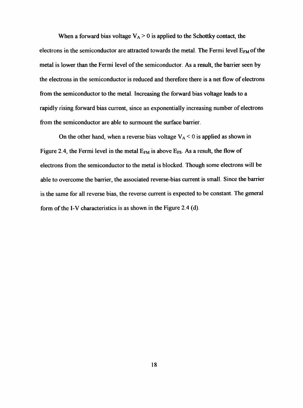
When a forward bias voltage VA > 0 is applied to the Schottky contact, the
electrons in the semiconductor are attracted towards the metal. The Fermi level EFM of the
metal is lower than the Fermi level of the semiconductor. As a result, the barrier seen by
the electrons in the semiconductor is reduced and therefore there is a net flow of electrons
from the semiconductor to the metal. Increasing the forward bias voltage leads to a
rapidly rising forward bias current, since an exponentially increasing number of electrons
from the semiconductor are able to surmount the surface barrier.
On the other hand, when a reverse bias voltage VA < 0 is applied as shown in
Figure 2.4, the Fermi level in the metal EFM is above EFS- AS a result, the flow of
electrons from the semiconductor to the metal is blocked. Though some electrons will be
able to overcome the barrier, the associated reverse-bias current is small. Since the barrier
is the same for all reverse bias, the reverse current is expected to be constant. The general
form of the I-V characteristics is as shown in the Figure 2.4 (d).
18

VA^ W5M n-typc semiconductOT
(a)
^VM K
(b)
• >
•*V.
Figure 2.4 Response of bias voltage to a Schottky diode 23
19

2.3 Ohmic Contacts
An ohmic contact is a metal contact to a semiconductor that has a very small
contact resistance compared to the bulk of the semiconductor. They are essential for
extracting electrical characteristics of a semiconductor device and is considered an
extremely important process step for fabricating high-performance semiconductor
devices and integrated circuits. An ohmic contact is a non-rectifying contact in which the
current-voltage relation under both reverse and forward bias conditions is linear and
symmetrical. Typical I-V characteristics of an ohmic contact is shown in Figure 2.5.
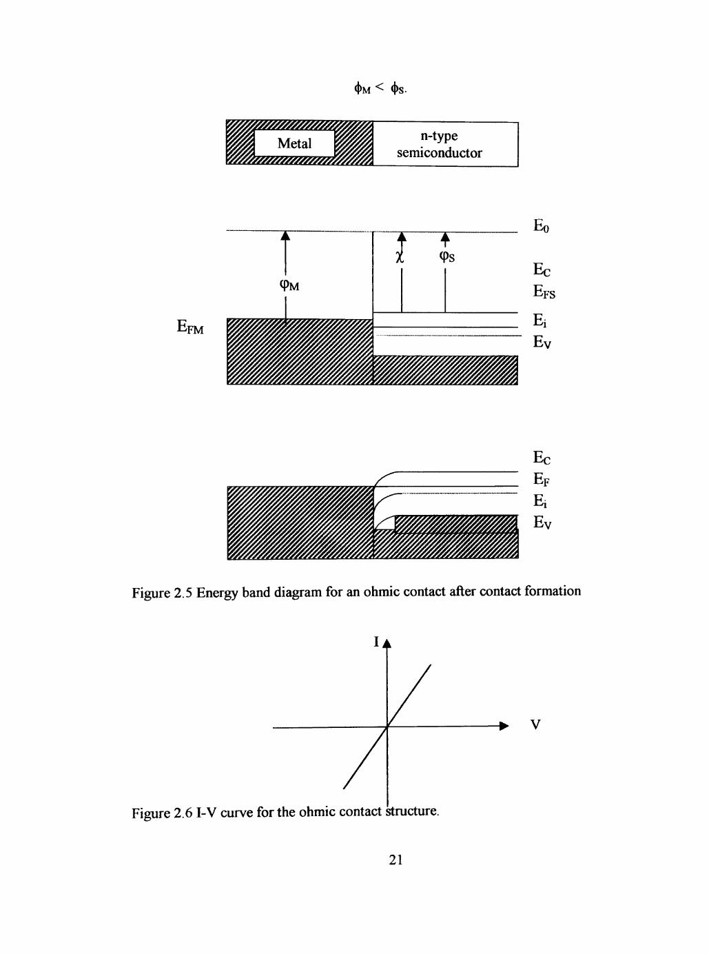
The energy band diagram for a metal and semiconductor with ^M < (j)s is shown in
Figure 2.6. From the figure it is clear that there is no barrier of any kind for electrons to
flow from the semiconductor to the metal. Thus even when a small forward voltage is
applied to the metal-semiconductor contact, it gives rise to a large forward bias current.
In the reverse bias condition, a small barrier is encountered by the electrons flow, from
the metal to the semiconductor, but the barrier essentially vanishes if the reverse bias
exceeds a few tenths of a volt. Thus large reverse currents are expected at relatively small
reverse biases.
The overall conclusion is that MS contact formed from a metal and an n-type
semiconductor will be rectifying if (J)M > <t>s and ohmic if^u < <j>s-
Table 2.3 Electrical Nature of Ideal MS Contacts
(t>M > <|>S
<t>M < <t>S
n-type Semiconductor Rectifying
Ohmic
p-type Semiconductor
Ohmic
Rectifying
20
<t>M < <|>S.
'FM
Ec EF
E, Ev
Figure 2.5 Energy band diagram for an ohmic contact after contact formation
• V
Figure 2.6 I-V curve for the ohmic contact structure
21
2.4 High-Ouality Schottky Diode
High Quality Schottky diodes are characterized by:
1. Very large breakdown voltages.
2. The ideality factor should be approximately equal one.
3. There should be a small interface layer between the semiconductor and the metal.
2.5 AppHcations of Schottkv Diodes
The Schottky diode is electrically similar to the abrupt one-sided p-n junction
diode, but there is a major difference between the two; the Schottky diode, unlike the p-n
junction diode, in most cases operates as a majority-carrier device in which the minority-
carrier transport and storage are nearly absent. As a consequence, Schottky devices have
a high switching speed and are suitable for high-speed application such as digital
switches and are also used in various device applications such as Metal Gate Field Effect
Transistor (MESFETs), photodetectors, solar cells, modulation doped field effect
transistors (MODFETSs), Schottky transistor logic gate arrays (SLT), microwave mixers,
Schottky-clamped transistors. They can also be used as a variable capacitor in parametric
circuits for frequency multiplication. The Schottky barrier solar cell has the potential for
use as a low-cost photovoltaic power conversion device for large-scale terrestrial power
generation. High-speed Schottky barrier photodector covering a broad wavelength range
from ultraviolet to visible and into far-infrared have been reported using different metal-
semiconductor materials. The logarithmic relationship displayed by the I-V curve of a
Schottky diode under forward-bias conditions over several decades of current change
enable it to be used in the logarithmic converter circuits. "^
22

2.6 Other Work
To improve the device performances of the semiconductor devices, high-quality
and reliable ohmic and Schottky contacts are required. Several research studies have
closely examined the electrical characteristics of metal contacts to n-GaN semiconductor.
Different metals have been examined so far. This section describes the work done by
several different groups.
2.6.1 Schottky Contacts to n-GaN
Schottky barrier contacts on GaN using different metals have been reported so far.
This includes the metals Pt, ' " ' Pd, ''''^ Au, '"- ^ Ni, " ' Rc}''^ Ag. l Figure 2.7
provides a summary of reported barrier heights plotted against the work fijnction of the
metal from various sources.
9 £ g> 0) X k. 0) *c k-(Q 03 • * ^
•5 x: u W
U.D -
0.4 -
xj.Z. -
o.u - I 1 1 1 1 1
•
•
•
^
•
. . . . . . . .
T T
. . . •
. . . .
• Ag • Re • Au • Pd • Ni T R
4.0 4.2 44 46 4.8 50 5.2 5.4 5.6 5.8 6.0
Metal Work Function (eV)
Figure 2.7 Reported Schottky barrier heights versus Metal work fiinction of metals.
23
All the data were complied from different labs using different ways of
metallisation, and the GaN were of varying quality. As a resuh there is considerable
scatter in the data. The barrier heights obtained by current-vohage and capacitance-
voltage methods differed in value. The difference was explained to be due to image force
lowering. The measured barrier height was found to be a fijnction of the difference
between the metal work fimction and the electron affmity of GaN. The typical values of
the barrier height for the metals were 1.5 eV for Pd, ' ^U. 1 eV for Pt, ^ ^ 0.9-1.15 eV
for Au, ^ ' ^ 0.66-0.99 eV for Ni. ^ ' ^
The influence of thermal treatments to the Schottky diodes on GaN were also
investigated by many research groups. The indium tin oxide schottky contacts on n-
(3a]sjH4] j.gpQj g(j ^ barrier height of 0.95 eV after annealing at a temperature of 600°C.
The Re '* ^ Schottky contacts reported a barrier height of 1.06 eV and did not degrade
upon annealing untill 700^C for 10 min. While the characteristics of other Schottky
diodes were reported to degrade after a mild thermal treatment as low as 300 C for
Pd,l'' 400Y for Pt,t ^ 575V for Au ' and 600V for Ni. '
Thermally stable PtSi'' ^ with a barrier height of 0.87 eV was reported and the
diodes did not degrade untill 500' C. NiSi " ^ Schottky contacts on n-GaN with a barrier
height of 0.8-1.0 eV and stable untill 600V were also reported.
24
2.6.2 Ohmic Contacts to n-GaN
Group in nitrides pose a problem in the development of low resistance ohmic
contacts due to their wide band gaps. In order to achieve high-performance GaN devices,
reliable ohmic contacts are necessary. Different combinations of metals have been
investigated for this purpose. Table 2.4 summarizes recent reports of ohmic contacts on
n-GaN.
The commonly accepted ohmic contact to n-GaN is the combination of Ti/Al
metallisation. In most cases, a TiN layer was formed as an interface layer and helped in
the formation of a low resistance ohmic contact. Researchers have suggested that the
formation of the nitride layer through the reaction with GaN causes N vacancies which in
turn resulted in the doping of the GaN and thus increased the carrier transport by
tunneling.
Ultra-low resistive ohmic contacts on n-GaN " ^ was reported using Si
implantation. Si was implanted at a doping density of 4 x 10 cm" to decrease the
contact resistance of the contact. Ti/TiN and Zr/ZrN ohmic contacts presents a thermally
stable contact at 600^C and also provided a smooth surface morphology. Ti/Al/Ni/Au
combination exhibited better surface morphology than the Ti/Al counterparts.
W contact was found to produce low resistance ohmic contacts to n-GaN with less
interaction between the semiconductor and the metal till 800°C. ^ ^ Thus for high
temperature electronic device applications, refractory metal contacts like W is more
preferable.
25

Table 2.4 Report on the ohmic contact to n-GaN by different research groups [69]
Metallization (nm) Ti/Al/Ni/Au (15/220/40/50) Ti/Al (20/100) Ti/Al (35/115) Ti (20) Ti/TiN (5/200) Ti/Ag (15/150) Ti/Ni (5/25) Ti/Au (3/300) Ti/Pd/Ni (5/5/25) TiN (200) Al (150) Al (250) W (50) Zr/ZrN (20/80) Pd/Al (12.5/100) Ta/Al (35/115)
Annealing Conditions
900"C, 30 sec
900^ , 30 sec
600V, 15sec
975"C, 30 sec
800"C, 60 sec
No anneal
1040^,30 sec
No anneal
990"C, 20 sec
800"C, 60 sec
600"C, 60-480 sec in Ar/H2 No anneal
600-1000"C,60sec
1000"C,60sec
650"C, 30 sec
600"C, 15sec
T
Carrier Concentration(cm')
4 x 1 0 ' '
10'^
5 x 1 0 "
5 x 1 0 ' '
7 x 1 0 "
1.7x10'^
1 x 1 0 ' '
4x10^"
1 x 1 0 "
7 x 1 0 "
7 x 1 0 "
5x10'^
1.5x10'^
2 x 1 0 ' '
2 .8x10"
7 x 1 0 "
References
[49]
[50]
[51]
[52]
[53]
[54]
[55]
[56]
[55]
[57]
[51]
[58]
[59]
[53]
[60]
[61]
26

CHAPTER m
CHARACTERIZATION
3.1 Semiconductor Device Characterization Techniques
Semiconductor material and device characterization falls into three main
categories:
• Optical characterization,
• Physical/Chemical characterization,
• Electrical characterization.
3.1.1 Optical Characterization
The optical characterization methods are used to determine the physical device
dimensions, layer thickness, concentrations, impurity and defect identification and
absorption and reflection coefficients of the semiconductor. Optical characterization
techniques include:
Optical microscopy,
Ellipsometry,
Photoluminescence (PL),
Transmission spectroscopy.
Absorption spectroscopy,
Raman spectroscopy.
Reflectance modulation,
Cathodoluminescence.
27

Optical microscopy gives images of the surface; ellipsometry yields insulator
thickness; photoluminescence is used for measuring shallow-level impurities. Raman
spectroscopy lends itself to small-area organic contaminant characterization and stress
measurements, while infrared reflectance is used for epitaxial layer thickness
measurements.
3.1.2 Physical/Chemical characterization methods
The Physical/Chemical characterization techniques are very important in finding
the spatial distribution of impurities, theu" identity and density, the structural and visual
information, defect parameters, the composition of compounds and their properties not
amenable to electrical or optical characterization. The Physical/Chemical characterization
methods include
• Electron beam techinques-
Scanning electron microscope (SEM),
Transmission electron microscopy (TEM),
Auger electron spectroscopy (AES),
Electron microprobe (EMP);
• Ion beam techniques-
Sputtering,
Secondary ion mass spectroscopy (SIMS),
Rutherford backscattering (RBS);
• X-ray techniques-
X-ray fluorescence (XRF),
28
X-ray photoelectron spectroscopy (XPS),
X-ray topography.
X-ray diffraction;
• Chemical etching.
The sensitivity of chemical and physical methods are generally poorer than the
electrical or optical techniques, but the spatial resolution can be extremely high with
atomic resolution possible in high-resolution transmission electron microscopy.
4.1.3 Electrical Characterization
Electrical characterization is the most common characterization method. It gives
electrically relevant information but is generally does not uniquely identify impurities the
way other two techniques do. The most usefial parameters determined by electrical
characterization techniques are:
• Resistivity,
• Carrier concentration,
• Mobility,
• Contact resistance,
• Barrier height.
Among the electrical methods the capacitance-vohage, the spreading resistance
and the Hall-effect techniques are most commonly used. The work described in this thesis
uses the capacitance-voltage and current-voltage characterization techniques.
29

3.2 Capacitance-Voltage Measurements
The differential capacitance of a depletion layer, formed by a Schottky barrier,
can be used to determine the majority carrier-concentration, barrier height, and also
determine the presence of interfacial layer. This section deals with the theory of
capacitance-voltage (C-V) measurement.
3.2.1 Capacitance of a Schottky barrier
Consider the band diagram of a Schottky diode between a n-semiconductor and a
metal as shown in Figure 3.1.
E'^F
Figure 3.1 Band diagram of Schottky barrier in reverse bias.
30
In Figure 3.1, the solid lines correspond to the reverse bias voltage VR and the
dashed lines corresponds to an increase in the reverse bias F^ + AF^ . When the reverse
bias voltage is increased, the electrons in the conduction band of the semiconductor will
move away from the metal and as a result the width of the depletion region will increase
from v/to w + Aw. Near the interface between the semiconductor and the metal there is a
significant hole concentration which will decrease as the hole quasi-Fermi level will
become equal to the metal Fermi level. The fluctuations of charge in the depletion region
gives rise to capacitance. This is same as that which takes place inside a parallel plate
capacitor.
In the barrier region three sources of charges are present: (1) A positive charge Qd
in the depletion region due to the uncompensated donors. (2) The extra holes in the
valence band constitute a positive charge Qh. (3) The electrons on the surface of the metal
constitute a negative charge Qm. When the applied bias is increased the total current in
the depletion region consists of a conduction current and a displacement current. The
conduction current consists of two current densities. One is due to the drift and difhision
of electrons to the metal from the semiconductor, and is represented as Jd, and the other
is due to the flow of charge carriers in the depletion region as the bias is increased and is
represented by Jc2- The displacement current density arises due to the electric field in the
depletion region and is represented by Jd.
Figure 3.2 shows the charge density due to the electrons and holes. At x = xi, the
difference between the metal Fermi level and the Valence band is greater than
^ + 3kT Iq ans so the hole density at this place is less than Nd, while at x = X2, the \
31

charge due to holes
charge due to electrons
Figure 3.2 Charge density due to mobile carriers.
electron density is less than Nd. therefore in the range between xi and X2, the charge
density is due to the donors. The conduction current density component hi is zero in this
region and thus, the capacitive current is due to the displacement current density Jd.
J^ =s,dE/dt. (3.1)
From the definition of capacitance
Jj=C{dAVj,ldt). (3.2)
Where C is the differential capacitance per unit area.
Equating equations 3.1 and 3.2, we get
C{dAVji/dt) =s,dE/dt (3.3)
32

C = £„ dE
dV, R
(3.4)
By applying Gauss theorem, the field strength is calculated.'''
s,AE = AQ, (3.5)
differentiating both sides with respect to VR, we get
dE _dQ,
dV^ dV^ (3.6)
Substituting equation 3.6 in 3.4 we get
C _dQ,
dV, R
(3.7)
In the case where minority carriers can be neglected, the differential capacitance
is given by the diffusion voltage and donor density. In this case the metal Fermi level is
above the valence band by at least ^ + 3kT I q. The electric field is given by [11
E' = ^ max
r r
's V
F. V
kT^ +
kTN. exp kT J \
(3.8)
Where Vd = diffusion voltage .
Assuming the condition qVd > 3kT , equation 3.8 will become
E" = ^ / /
A . V
V, V
KT\
1)j
(3.9) 11]
From Gauss theorem, the charge is given by
a=^s^. max (3.10)
Substituting 3.9 in equation 3.10, we get
33

1 A:
Q,={2qe,NMv, f . (3.11) V ^ )
From equation 3.7,
c = ,s,N,A^\^(^^^^^^_,y.i 3 ^
V "- y ^
where F ^ = F ^ , + r ^ .
Vdo is the dififusion voltage at zero bias.
If both sides of the equation are inverted and then squared, one obtains
C qN^K^s^A^ V / 'iJ
Equation indicates that a plot of 1/C versus VA should be a straight line where
the slope is inversely proportional to the carrier concentration, the carrier concentration is
given by
N, qKss^A slope
and the intercept of x-axis, Vo, is related to the built-in voltage Vdo via
Vdo == Vo + kT/q,
where T is the absolute temperature.
The barrier height ^B is calculated using the relation
(|)B = q ( Vdo + Vn )
where Vn = (kT/q)ln(Nc/Nd)
34

where Nc is the effective density of states and is given by the equation
Nr=2 c 27071 kT^ ^
(3,14)
m the effective mass for the GaN is related as
m* =7Wo0.22
where mo is the electron rest mass 9.11x10 ~ ^ kg.
The effective density of states for GaN is calculated to be 2.8 x 10 ^ cm' .
A Schottky diode consists of a junction capacitance C, a junction conductance G,
and a series resistance Rs . In the parallel mode, the measured capacitance Cm is related
to the true junction capacitance C by
C = ^ '" (l + RsGf + {iTtfCRsf
where f is the measurement frequency. The value of Cm approaches C, when R s G « l
and (^nfRsCf < 1.
The conductance G is very negligible and is ignored. The series resistance at lower
frequency like 10 KHz is negligible. The series resistance for different frequencies is
calculated by
wCXC. m
and the capacitance for different frequencies is then given by
^J-4\-4{wRsCj 2C^{wRsf
35

3.3 I-V Characteristics
The forward current-voltage (I-V) characteristics of a Schottky diode obyeing the
thermionic emisson model is given by
1 = 1, exp V 'kT - 1 (3.15)
Where q is the electronic charge,
VD is the applied voltage across the junction,
k is the Boltzmann constant,
T the absolute temperature,
15 is the saturation current.
However, most practical Schottky diodes show deviations from ideal thermionic
emission behavior. A dimensionless parameter called the ideality factor, n , is usually
included in the I-V relationship to take into account the nonideal behavior. ^
I = Is 'A'WnkT^-' J
(3.16)
The saturation current Is can expressed as
/, = ^^^T^exp(-^^«4] (3.17)
where Aeff is the effective area of the diode,
A* is the Richardson constant,
(l>g is the Schottky barrier height of the diode.
The theoretical value for the effective Richardson constant is given by the
36
^•^Anqm'ky^^ (3.18)
where h is the planks constant
and m is the effective mass of the semiconductor.
The value of the Richardson constant for GaN was calculated to be 26 A cm' K' .
The effect of series resistance R is modeled as a series combination of a reisitor
and a diode. The voltage VD across the diode is given by
V^=V-IR
where I is the current flowing through the resistor.
Equation 4.16 will be written as
i=h (^'-'% ' 1 ' '/nkT]-^ (3.19)
The value of the series resistance R is deduced using the method of Cheung and
Cheung, f ^
In this method equation (3.19) is rewritten in terms of current density.
V = RA,ffJ + n^, ^ifpHyA^T^] ^ °
where p - yiyr •
Differentiating and rearranging equation (3.20)
t/(ln J) "^ P
One can determine the value of the series resistance by making a plot of
37

dV ^ft rx vs J . The plot is a straight line with the slope equal to RAeff and the y-axis
intercept will be y^.
Once the value of the series resistance is calculated, the applied voltage V is corrected for
/
the series voltage drop IR, A plot of In
\
1 - e x p '-qV^^
V/ V f^T J J
vsVj-, will give q/nkT as
the slope and extrapolated intercept with the current axis gives Is. From this Is value ^
can be calculated as
= yin ^AA*T'^
y ^s J
38
CHAPTER IV
EXPERIMENTAL PROCEDURE USED
FOR THE FABRICATION OF THE SCHOTTKY DIODES
This chapter explains the processing steps used for the fabrication of Schottky
diodes. The structure of the GaN sample, the structure of the various mask used for
making different Schottky diodes, the fabrication procedure, and the experimental set-up
used to make the contacts are discussed in this chapter.
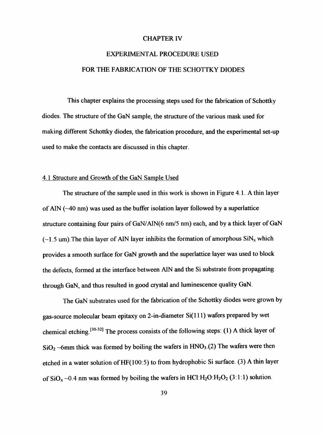
4.1 Structure and Growth of the GaN Sample Used
The structure of the sample used in this work is shown in Figure 4.1. A thin layer
of AIN (-40 nm) was used as the buffer isolation layer followed by a superlattice
structure containing four pairs of GaN/AlN(6 nm/5 nm) each, and by a thick layer of GaN
(-1.5 um).The thin layer of AIN layer inhibits the formation of amorphous SiNx which
provides a smooth surface for GaN growth and the superlattice layer was used to block
the defects, formed at the interface between AIN and the Si substrate from propagating
through GaN, and thus resuhed in good crystal and luminescence quality GaN.
The GaN substrates used for the fabrication of the Schottky diodes were grown by
gas-source molecular beam epitaxy on 2-in-diameter Si(l 11) wafers prepared by wet
chemical etching. ^ ' ^ The process consists of the following steps: (1) A thick layer of
Si02 ~6mm thick was formed by boiling the wafers in HN03.(2) The wafers were then
etched in a water solution of HF(100:5) to from hydrophobic Si surface. (3) A thin layer
of SiOx -0.4 nm was formed by boiling the wafers in HC1:H20:H202 (3:1:1) solution
39
(4) The wafers were then etched in HF:ethanol (1:4) to from a hydrogen saturated
surface. The growth process was initiated by exposing the Si substrate to Al flux for 1-2 s
followed by 1-2 s exposure of ammonia. This procedure was repeated 5-10 times and it
resulted in the suppression of amorphous silicon nitride islands. The AIN buffer layer was
grown by turning on the ammonia and Al together with the NH3 beam equivalent
pressure of (0.5-3)xlO'^ Torr at a temperature of 1160 ± 30K. The entire 40 nm AIN
growth took ten minutes. After the growth of AIN buffer layer was completed, the
superlattice structure containg four pairs of GaN/AIN (6 nm/5 nm) was grown and was
then followed by the growth of GaN. The source material used was effusion cell for Ga
and Al. The growth was done at a temperature of 1000 K and growth rates of 0.4-1.1
|j,m/h. [30-32]
1.5 iin GaN
Superlattices (GaN/AlN)
40nmAlN
n-type Si(l 11)
Figure 4.1 Cross-sectional structure of the sample used in the experiment.
40

4.2 Mask Used for the Fabrication Process
A mask is defined as a pattern tool, which contains patterns that can be
transferred to an entire wafer in one exposure.
Two different processing techniques were used to fabricate different Schottky
diodes. Each of these two methods used a different mask. They are
• One-mask process.
• Two-mask process.
The following section explains the different mask used and also depicts the
cross-sectional view of the diode structure.
4.2.1 One-Mask process
The top view of the diode configuration used for transferring the pattern in the
one mask process is as shovm in Figure 4.2. The dark areas are exposed to the light and
metal is deposited in this area and the unexposed region is protected by the photoresist
and the metal on this region is removed during the lift-off process. The metal pattern in
the circular region is used as the Schottky contact and the large area metallization is used
as a low resistivity contact or the ohmic contact. The metals used in this process for
Schottky contacts were Au and Ni, respectively.
The cross-sectional view of the Schottky diode using the one mask process is
shown in the Figure 4.3. The diameter of the circular region, which forms the Schottky
contact is 200 /i m.
41

Figure 4.2 Top view of the diode configuration used in one-mask process.
Schottky contact Ohmic Contact
n-GaN
Superlattices
A I N
n-Si(l l l)
Figure 4.3 Cross-sectional view of the diode structure in the one-mask process.
4.2.2 Two-Mask process
In this process, two mask were used. One mask was used to transfer the ohmic
contact pattern and the other mask was used to transfer the Schottky contact pattern to the
wafer. The structure of the two mask are as shown in Figure 4.4 and Figure 4.6,
respectively.
42

Figure 4.4 Top view of the ohmic contact configuration used in two-mask process.
Ohmic Contact
n-GaN
Superlattices
AIN n-Si(l l l)
Figure 4.5 Cross-sectional view of the ohmic contact structure in two-mask process.
In Figure 4.4, the dark areas are exposed during the exposure and the metal is
deposited in these regions and it constitutes the ohmic contact. The circular region is
unexposed and has a diameter of 300 um and is protected by the photoresist during the
deposition of ohmic contact. After the first-mask process, the cross-sectional view of the
ohmic contact structure is as shown in Figure 4.5
The top view of the second mask used for transferring the Schottky structures is
shown in Figure 4.6. The dark circle is 200 pm in diameter. The circular region is
exposed and metal is patterned in this structure and forms the Schottky contact, the
unexposed regions containing the ohmic contact pattern obtained from the first mask is
43

covered with photoresist and thus are protected during the pattering of the Schottky
contact.
Figure 4.6 Top view of the Schottky contact configuration used in the two-mask process.
Schottky contact Ohmic Contact
n-GaN
Superlattices
AIN n-Si(l l l)
Figure 4.7 Cross-sectional view of the diode structure in the two-mask process.
44
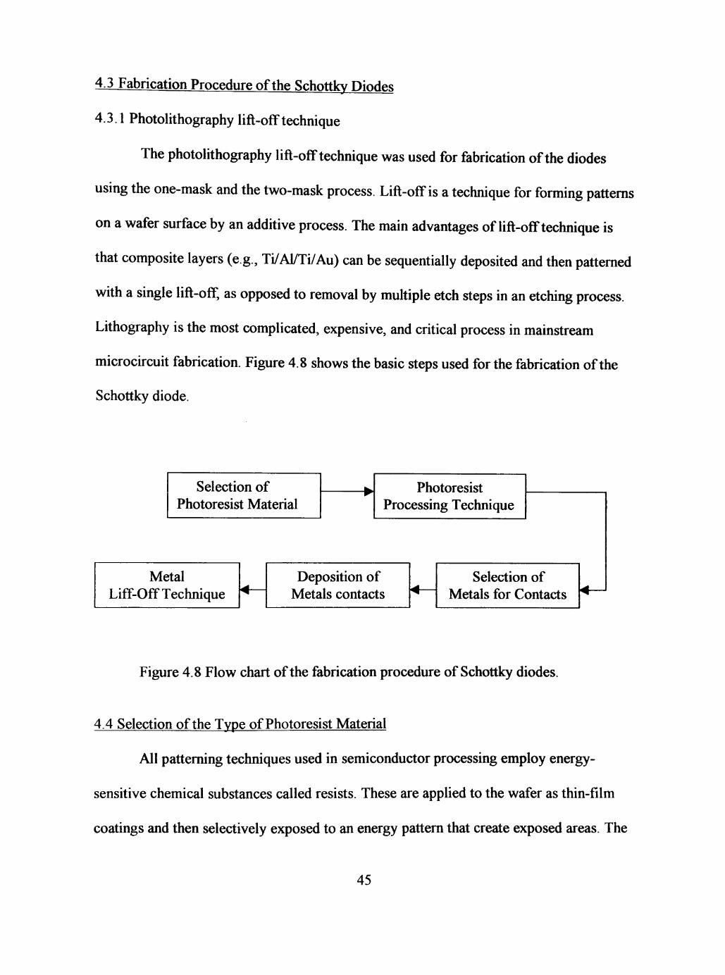
4.3 Fabrication Procedure of the Schottkv Diodes
4.3.1 Photolithography lift-off technique
The photolithography lift-off technique was used for fabrication of the diodes
using the one-mask and the two-mask process. Lift-off is a technique for forming patterns
on a wafer surface by an additive process. The main advantages of lift-off technique is
that composite layers (e.g., Ti/Al/Ti/Au) can be sequentially deposited and then patterned
with a single lift-off, as opposed to removal by multiple etch steps in an etching process.
Lithography is the most complicated, expensive, and critical process in mainstream
microcircuit fabrication. Figure 4.8 shows the basic steps used for the fabrication of the
Schottky diode.
Selection of Photoresist Material
Metal Liff-Off Technique
Photoresist Processing Technique
Deposition of Metals contacts
Selection of Metals for Contacts
Figure 4.8 Flow chart of the fabrication procedure of Schottky diodes.
4.4 Selection of the Type of Photoresist Material
All patterning techniques used in semiconductor processing employ energy-
sensitive chemical substances called resists. These are applied to the wafer as thin-film
coatings and then selectively exposed to an energy pattern that create exposed areas. The
45
resist film is then subjected to a development process that selectively removes either the
exposed or the unexposed resist. There are two types of photoresist used in the VLSI
applications
• Positive photoresist.
• Negative photoresist.
Positive photoresist are those in which the development removes the exposed
regions. And negative photoresist are those in which the development removes the
unexposed resist. The high resolution capabilities of positive photoresist have made them
the exclusive choice for VLSI applications. Conventional positive lithographic process
and resists are capable of producing images on the surface with dimensions as small as
0.13 p m. For the fabrication of the Schottky diode in the lab, SHIPLEY S1813 PR
positive photoresist was used.
4.5 Photoresist Processing Technique
The whole processing technique was done in the clean room in the lab. The basic
steps that comprise the complete photoresist process used for the fabrication of the
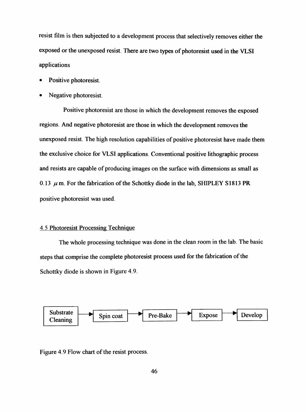
Schottky diode is shown in Figure 4.9.
Substrate Cleaning
• Spin coat • Pre-Bake • Expose • Develop
Figure 4.9 Flow chart of the resist process.
46
4.5.1 Substrate cleaning
The cleaning of the substrate surface is a very important step in the fabrication of
devices, especially in the fabrication of schottky diodes. Surface cleaning has a
significant influence on the metal-substrate contact resistance/stability and overall device
quality (Schottky diode). ^ " ^ The cleaning step helps in the removal of native oxides,
organic contaminants and residual species. Chemical purity is very important, and the
conunonly used solvents, acids, and bases are the semiconductor grade (SC grade), which
is one step above reagent grade. The GaN samples were first ultrasonically cleaned with
semiconductor grade organic solvents (acetone and Methanol), followed by dipping in
Buffered HF for 20 seconds, rinsed with DI water and dried in N2 gas. In some cases, the
samples are in their cleanest form as they are removed immediately after being formed
and in such cases fiirther cleaning was avoided.
4.5.2 Spin Coating
After cleaning, the wafers are coated with the photoresist. Spin coating is the widely
used technique to produce a uniform layer of photoreist of desired thickness over the
wafer. It involves three steps:
• The photoresist is dispensed onto the wafer.
• The wafer is accelerated to a final rotational speed.
• The wafers are spun at a constant speed for a specified time.
The ECIOIDT and PMIOIDT Series of Photo Resist Spinners (Headway
Research, Inc.) were used for this purpose.
47
In the first step, a small volume of the positive photoresist solution was dispensed
at the center of the wafer. Following this, the wafer was accelerated quickly to the final
spin speed. Normally, in this stage, high ramping rates are preferred as they yield better
film uniformities since the solvent in the resist evaporates rapidly from the resist. In the
third step, the wafer is spun for some time to produce a relatively uniform flow profile.
The spinning cycle consists of solvent evaporation to produce the solid film. In the
fabrication process, a final spin-speed in the range 5000-6000 rpm range for 30 sec was
used.
4.5.3 Pre-Bake
After the wafers are coated with the photoresist, they are baked to a temperature of
120* C for 60 sec. This step is called the soft-bake or pre-bake. This step is used to:
• Drive off the solvent from the photoresist and thus improves the adhesion of the
substrate with the photoresist during the development step.
• Anneals stresses caused by the spinning process. ^^^
Several types of oven are used for the pre-bake process. The most commonly used
ones are (a) convection; (b) infrared; and (c) hot plate ovens. Each of these uses different
heat transfer mechanisms. In the convection oven, the hot air transports the heat to the
wafer. The normal duration a soft-bake cycle in a convection oven is -30 minutes. In the
infrared ovens, long wavelength IR penetrates the resist film and is reflected back by the
photoresist substrate interface. For the resist processing of the Schottky diodes in the lab,
a hot-plate oven was used. In this technique the resist is heated quickly to the desired
temperature. The bake cycle used is 60 sec at a temperature of 120 C.
48
4.5.4 Exposure
After the wafer was cleaned, coated with the resist and suitably soft-baked, it is
ready to be exposed to optically transfer the pattern on the mask to the resist coated
wafer. There are different methods to do this like contact printing, proximity printing,
projection printing, and optical stepping.
In proximity printing, the mask and the wafer are not in contact but are placed
close to one another during exposure. Light passes through the mask and exposes the
resist on the wafer as shown in the Figure 4.10.
In projection printing, the mask and the wafer are separated from each other and
optics are used to image the mask pattern onto the wafer.
In optical stepper technique a mask, called a reticle, contains the pattern. This
pattern is imaged onto the wafer, and then the wafer is moved, and the exposure is
repeated. This procedure continues until the entire wafer is exposed with the pattern.
For the fabrication of the Schottky diodes in the lab, the contact printing
technique was used. In contact printing, the mask is pressed against the resist coated
wafer during exposure. Figure 4.10 (b) shows the exposure system. The mask is held
chrome side down in a frame and is loaded. After the wafer is aligned to the mask, the
wafer was exposed by the radiation from a high intensity Hg-arc lamp.
A CANON Parallel Light Mask Aligner PLA-501F was used to expose the wafers
in the lab. The exposure time used for the fabrication of the diodes was 20 sec. After
exposure, the photoresist was developed.
49

i I I I 1 /
a)
MASK
RESIST COVERED SLICE
11111 MASK
b)
SLICE i RETICLE MOVE
, ^
I
c)
\J \
\ RETICLE
SLIT MIRROR
I I t M i i
\ RETICLE
Figure 4.10 Major methods of exposure technique
(a) Proximity; (b) Contact; (c) Projection; (d) Optical stepping.
50
4.5.5 Development
After exposure, the photoresist is developed to produce the image, which is used
as a mask for lift-off. The main purpose of the development process is to effectively
produce the specified pattern on the wafer with minimum distortions or swelling. The
development time is normally kept short.
The positive resist developers are alkaline solutions diluted with water. SHIPLEY
MICROPOSIT DEVELOPER CONCENTRATE positive photo resist developer was
used for the development of the pattern for the diodes in the lab. The development
solution contained developer and water in 1:1 ratio. As a result, the wafer required only a
water rinse before it was blown dry. During the develop cycle, in the exposed areas, the
carboxylic acid reacts with the developer to form amines and metallic salts, which then
rapidly dissolve in the developer solution. In the unexposed areas, no such groups are
formed and these regions are unaffected by the developer. The development time used in
the process was 20 sec.
After development, the wafers are rinsed in DI water. Proper rinsing in DI water
is required as the developing action continues until the developer is completely removed
from the resist surface. The substrate is rinsed for more than 30 sec and then is blown
dry.
4.6 Choice of the Metals Used for Making the Ohmic and Schottky Contacts
According to the Schottky-Mott model, the barrier height equals the difference
between the metal workfimction and the electron affmity of the semiconductor x • The
51
electron affmity of GaN - 4.1 eV. The workfimction of Au and Ni is 5.1 and 5.15,
respectively, and thus was choosen to form Schottky diodes. Schottky contacts were
fabricated by evaporating Au and Ni respectively. The thickness of the Schottky contacts
were 1000 A and were circular in shape with a diameter of 200//w .
A composite metal layer of Ti/Al/Ti/Au(300 A /700 A /300 A /500 A) formed the
ohmic contact configuration. Electron beam evaporation was used to deposit the layer.
4.7 Deposition Technology
4.7.1 Physical Vapor Deposition by Evaporation
The ohmic and Schottky contacts necessary for the fabrication of a Schottky diode
are deposited using evaporation technique. In this process the source material is heated
thereby causing evaporation. The evaporation is done in high-vacuum conditions
typically in the range of 10~ to 10 torr. The vaporized molecules from the source
reach the substrate surface without collisions with any other gas molecules in the
deposition chamber. As a result the deposited film is as pure as the source material. The
main advantage of the evaporation process is that the substrate surface is not damaged
due to the low energy of the impinging atoms and moreover the films can be deposited at
higher rates. During the evaporation process as the source is heated, the pressure rises
somewhat as contaminants are desorbed from its surface.
4.8 The Evaporation Svstem Used for the Experiment
The evaporator used in the lab for the fabrication of the Schottky diode is shown
in Figure 4.11. The main parts of the evaporator can be divided into three main sections:
52

• Vacuum system,
• Chamber which includes the evaporating source, substrate holder, the crucible liners,
• Evaporation thickness controller.
This section explains the evaporation system followed by a brief summary of the
system configuration.
4.8.1 Vacuum system
The vacuum system consists of the rotary roughing pump and the cryogenic pump
as shown in Figure 4.11. The rotary roughing pump is a mechanical pump that transports,
compresses, and expels the gas. The gas expelled from a roughing pump is known to be
carcinogenic. Therefore a ventilation system is devised from 3-1/2 inch PVC tubing that
is directed to a roof vent. The rotary roughing pumps serves two purposes, first they are
used to pump vacuum chambers from atmosphere to the medium vacuum range in the
order of 10 torr. And second they serve as forepumps for the cryo pump.
A cryogenic pump, Cryo-Torr 8 Cryopump, is used to improve the vacuum. It
operates on the principle that gases can be condensed and held at extremely low vapor
pressures, achieving high speeds and throughputs. Cryogenic pumps are closed cycle
refrigerator pumps that removes gases from the vacuum chamber by capturing them on a
cold surface. The process of gas capture by high-vacuum cryopump involves both
cryocondensation and cryosorption. Cryocondensation refers to the condensation on a
surface whose temperature is cold enough that the vapor pressure of the condensed
substance is so low that the vapor is effectively removed from the system. Cryosorption
involves the adsorption without condensation of a gas on a cold surface.
53
Nj Puige
NjPuige
Vent Valve
Absorption Trap
Ron^ineValve
--•@TCGauge#2
Gate Valve
Ion Gauge
<5G)
TC Gauge i
Roughing Piunp
^ 7 \ / ) CiyoPump
Figure 4.11 The evaporation system used.
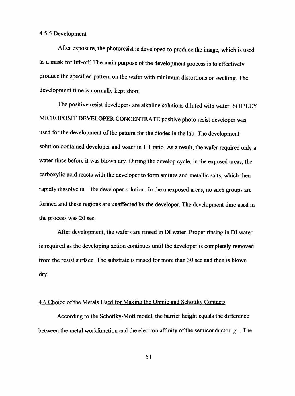
4.8.1.1 Vacuum procedure.Operating procedure requires that the cryopump
pressure is below 50 torr before turning on the compressor unit. The pressure in the
chamber is brought down to the operating level of the cyro pump by first turning the
roughing pump on. The procedure for the operation of the vacuum chamber is as follows.
• After loading the samples into the chamber the vacuum jar is completely lowered.
54
• With the Vent Valve and Collar Valve closed and the roughing pump on, the
roughing valve is opened. The pump is allowed to evacuate the chamber until the
pressure is about 10"^ torr.
• When adequate pressure is achieved, the roughing valve is closed and the gate valve
is opened. The cryo pump is turned on.
• The roughing pump is turned off and the vent valve is opened. The foreline pressure
is allowed to reach atmospheric pressure and then the vent valve is closed. This is
done to prevent the back-flow of oil vapors from the roughing pump to the cahmber.
• The pressure is allowed to reach the baseline pressure for deposition(~10 ~ torr)
Monitoring of the vacuum pressure is an important factor in the deposition of the
thin films. Since it is impossible to find a vacuum gauge that can give quantitative
measurements over the entire vacuum region of interest (10^^ - 10"^ torr), two vacuum
gauges are used, an ion gauge and a vacuum gauge. One is placed above the gate valve
and one below. This arrangement allows the monitoring of the pressure inside the cryo
pump and the chamber. The ionization gauge measures pressure in terms of the number
of density of molecules and has a measuring range from 10 to 10 torr. The Varian
low vacuum guage is a heat loss manometer, inferring the pressure of the gas by
measuring the thermal loss of a heated wire, and has a measuring range from atmospheric
pressure to 10~^torr. This gauge is used to indicate the actual pressure in the chamber
turning the roughing stage.
55

4.8.2 Vacuum Chamber
The vacuum chamber consists of the crucible liners, substrate holder, shutter, the
crystal detector and the evaporation source as shown in Figure 4.13.
4.8.2. ICrucible Liners.The crucible liners used for this work was a 2.2 cc 3kW e-
Gun liner with the following dimensions and is shown in Figure 4.12.
Table 4.1 Dimension of the crucible liners.
Dimensions
(A) Top Diameter
(B) Bottom Diameter
(C) Height
(D) Wall Angle
Measurements
.75"
.56"
.37"
15"
' ^
T
Figure 4.12 Crucible Liner
k«-
56

The Glassy Coated Graphite crucible liners were used for the evaporation of Au,
Al, and Ti source material. The glassy coated carbon graphite liners are made from high
grade carbon with a coated graphite process that is baked above 1,400^C to eliminate any
porosity in the carbon.
4.8.2.2 Evaporation source. There are three different types of crucible heating
systems: resistive, inductive, and electron beam systems. For the evaporation of the
source material in the lab, electron beam evaporation was used. In this technique, a
stream of electrons is accelerated to high kinetic energy. The beam is directed at the
material to be evaporated, and the kinetic energy is transformed to thermal energy upon
impact. The electron stream can melt and evaporate any material, provided the beam can
supply sufficient energy. The electron beam heating is an efficient and practical way of
achieving temperatures in excess of 3500^ C for uniform thin film deposition process.
The Thermionics e-Gun^^ source, which is bakeable to 250° C, and its control units, have
been chosen to be part of our evaporation system. Its simplicity and non-contaminating
operation makes it suitable for research activities. The features of the e-Gun is as
follows:
• The e-Gun^^ can be used to evaporate the metals required for the ohmic and
Schottky contacts.
• The source control unit has three safety interlocks that work in conjection with the
e-Gun evaporation source.
1. Water-flow interlock, to insure proper water flow to the unit.
2. Pressure interlock, to make sure the confrol unit won't operate above 1x10" torr.
57
3. Cabinet interlock, to make sure the power is safely disconnected when the rack
panel door is opened.
TM • The maximum output power of the e-Gun source is 3000 Watts
TM • The e-Gun source has 5 crucible positions.
• Each crucible will hold up to 2.5 c c of source material.
TM The e-Gun source control unit has two important accessories, which will allow
precise application of any standard evaporant.
• A deposition rate controller, which monitors the rate of deposition in angstroms per
minute.
• A thickness control monitor, which indicates the film thickness that is deposited.
'< > <: ^
^^^jr,a_jr*t,jr^^jn^j^^j^
m
Substrate Holder
fc. Shutter
_^ Crystal
^ Filament
Figure 4.13 Evaporation Chamber
58

4.8.3 Evaporation thickness control monitor
The block diagram of the thickness control monitor is shown in Figure 4.14.
Inficon Deposition Thickness Controller.
Vacuum guage Controller Ion Guage Controller
Thermionics e-Gun Source Control Unit.
Figure 4.14 Control Cabinet
The Inficon evaporation thickness controUer is placed at the highest position. The
Inficon IC/5 thin film deposition controller is equipped with a high frequency crystal
(6.0 MHz) and has a 0.00577 A rate resolution. It is a precise controller with a high
resolution capability, can define up to 50 processes, store recipes up to 250 layers for a
single process, and can use up to 24 materials. It also has a co-operation fimction, which
means two sources may operate concurrently.
59
4.8.4 Summary of system configuration
The e-gun beam evaporation system is configured as follows:
• Pumping system: An Alcatel M2008A, mechanical pump is employed to rough the
chamber. It takes about 10 minutes to drop the pressure inside the chamber to 1x10"
torr. A Helix CRYO-TORR 8 high vacuum pump is used to reach the high vacuum of
Q
10' torr. It takes about 5 hours to drop the pressure to high vacuum after switching
from the Alcatel mechanical pump to Helix CRYO-TORR pump.
• Chamber: It consists of a metal jar with a opening through which the crucible can be
viewed, power lines, vacuum gauges, cooling water circulation, displacer of the
crucibles, and crystal wires.
• Evaporation source. Thermionic e-Gun source is a 3 KW five position e-beam
source with 2.5 c c crucibles. The different metals are loaded in the crucibles and are
evaporated sequencially for the ohmic contacts.
• Deposition controller: The Inficon IC/5 Thin Film Deposition Controller is able to
provide small power rise steps for the Thermionic e-Gun^^ source control unit. The
rate of deposition was set to 5 A / sec.
• Substrate holder. The substrate holder was a square metallic holder with four circular
opening to hold four, two inch samples as shown in the Figure 4.13.
• Cooling system: A cooling system which provides constant water cooling when the
evaporation is in progress.
• Instrumentation: Two vacuum gauge controllers and a Thermionic e-Gun source
control unit constitutes the whole system.
60
4.9 Lift-Off Technique
After the evaporation of the contact, the wafer is subjected to the lift-off
technique. The wafers are immersed in a solution capable of dissolving the photoresist.
Semiconductor grade acetone is used for this purpose. The wafer is placed in acetone for
ten minutes and then is subjected to ultrasonic agitation. The metal that was deposited
directly on the semiconductor remains, while the metal deposited on the resist lifts off of
the wafer as the resist dissolves. The wafers are then cleaned in semiconductor grade
methanol, rinsed in de ionized water and are dried in N2.
For the two-mask process, after the deposition of the ohmic contacts, the wafers
were annealed for 2 minutes at 700°C in nitrogen ambient. After the annealing and
subsequent lift-off process, the wafers are again subjected to the photoresist procesing
steps to pattern the Schottky contacts, and thus are subjected to a total of two lift-off
processes.
4.10 Other Work Involving Different Device Geomentries
Several other device and contact geomentries were used by different research
groups in making Schottky diodes. These included lateral, mesa, and Schottky metal field
plate devices. The lateral Schottky rectifiers were similar to the one used in our lab for
this work. In some devices, large area Au metallization was used as a low resistivity
contact.
61
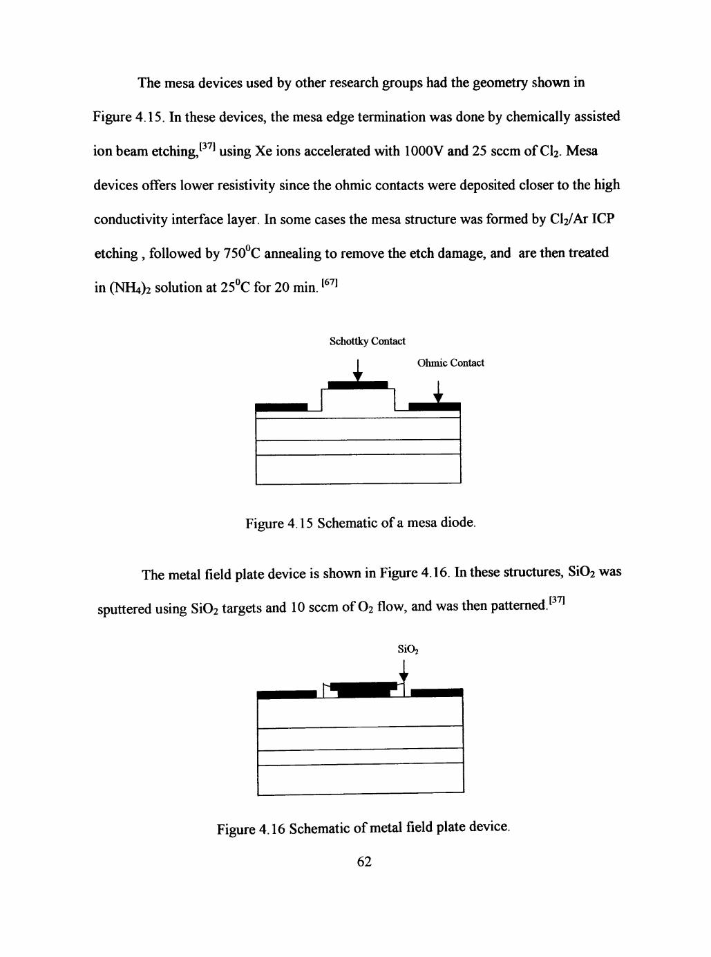
The mesa devices used by other research groups had the geometry shown in
Figure 4.15. In these devices, the mesa edge termination was done by chemically assisted
ion beam etching, ^ ^ using Xe ions accelerated with lOOOV and 25 seem of CI2. Mesa
devices offers lower resistivity since the ohmic contacts were deposited closer to the high
conductivity interface layer. In some cases the mesa structure was formed by CVAr ICP
etching, followed by 750°C annealing to remove the etch damage, and are then treated
in (NH4)2 solution at 25°C for 20 min. ^ ^
Schottky Contact
Ohmic Contact
Figure 4.15 Schematic of a mesa diode.
The metal field plate device is shown in Figure 4.16. In these structures, Si02 was
sputtered using Si02 targets and 10 seem of O2 flow, and was then patterned.
SiO,
Figure 4.16 Schematic of metal field plate device.
62

In some cases, a conventional photolithographic lift-off technique was used to define
Schottky diodes using the configuration as shown in Figure 4.17. ^^ The diodes had a
donut configuration with a diameter of 125 /jm . The configuration gave a relatively low
series resistance due to the small spacing between the contacts {-40 jam ) . The outer dark
colored ring formed the ohmic contact, while the circular region at the center formed the
Schottky contact.
OO GO
"• Schottky contact
-•Ohmic contact.
Figure 4.17 Schematic of a Schottky diode.
63

CHAPTER V
INVESTIGATION OF RESULTS AND DISCUSSION
In this thesis work, I report on the investigation of Schottky characteristics of Au
and Ni on n-GaN. Three different contact geometries were tested. The characteristics
were determined using I-V and C-V measurements. The measurements were done at
room temperature. The details of the fabrication of the diodes are dealt with in Chapter
III.
The metals Ni and Au was chosen for this study because both have a work
fiinction of 5.15eV and 5.1eV, respectively and could form good Schottky diodes with n-
GaN. Ni was chosen because it is more chemically active and provides better adhesions
to the samples.
5.1 Experiment
The GaN sample used in this study was n-GaN grown by gas-source molecular
beam epitaxy. The details of the grov^h procedure and fabrication process were discussed
in Chapter HI. Three different contact geomentries were taken into consideration. In each
of the different process, the electrical characteristics of Ni and Au Schottky diodes on n-
GaN were investigated. In the one mask process large area metallization formed the
ohmic contacts. In the two mask process, Ti(300A )/Al(700 A)/Ti(300 A)/Au(500 A)
multilayers formed the ohmic contact. Each diode fabricated was 200//w in diameter.
The distance between the adjacent ohmic and Schottky contacts is about 50 jum
64

The Capacitance-Voltage measurements were done with a HP 4275A Multi
frequency LCR meter. The data was captured with a Lab VIEW program. The I-V
measurements were done with a Keithley 2400 source meter and recorded using a
Lab VIEW program.
5.1.1 Capacitance -Voltage Measurements
The capacitance measurements of Ni and Au Schottky diodes were measured at
different frequencies raging from 10 KHz to 1 MHz between -6 V and 0 V.
The C-V relationship for a Schottky barrier is given by^ '
1 2 (.. „ kT-^ F., - V,
where s^ is permittivity of free space, Ks the dielectric constant of GaN, Vbi is the flat
band voltage, A is the area of the diodes, and VR is the applied voltage.
The capacitance and Cm is related according to
C = ^ " {\ + RGf+{27(fCRf
where f is the measurement frequency, R is the series resistance, and G is the junction
conductance. The value of the conductance was found to be very small and thus was
neglected.
Thus the capacitance was related by
c = ^
65

The value of Cm approaches C, when RG « 1 and (2;rfilC)^ « 1 . The series resistance at
lower frequencies was considered negligible. The value of series resistance was then
calculated for each frequency range. The barrier height and carrier concentration was
calculated from these measurements.
5.1.2 Current-Voltage Characteristics
The forwrad-biased I-V characteristics are described by the following equation:
-i'^'-'''ynkr)-^ I = Is
and
.**,
where Is is the saturation current, q is the electron charge, V is the applied voltage, Rs is
the series resistance, n is the ideality factor, A the effective Richardson constant, and
6g is the measured barrier height. The barrier height was determined using the theoretical
value of the Richardson constant.
The Richardson constant is given by
.** 47rem„k^
** .
A = h'
The electron effective mass for GaN is 0.22mo.The theoretical value of A' ' is 26 Acm'
It has been reported that A** value varies over a wide range of values for Schottky diodes
on GaN. ^ " ' ' Since a large variation in A** does not have a significant influence on the
66

deduced Barrier height (for example a variation of 100% in A * will resuh only in 1.8%
reduction in barrier height) and therefore the theoretical value was taken for calculations
5.2 Results and Discussions of Capacitance-Voltage Measurements using One-Mask process
The Capacitance-Voltage measurements for Au/n-GaN and Ni/n-GaN Schottky
diode for different frequencies are shown in Figure 5.1 and Figure 5.3, respectively. The
plot of 1/C vs V for different frequencies for Au and Ni Schottky diodes using the one
mask process are given in Figure 5.2 and Figure 5.4, respectively. The carrier
concentration and barrier height are calculated for Au and Ni Schottky diodes and are
summarized in Table 5.1 and Table 5.2.
67

Voltage (V)
Figure 5.1 Capacitance-Voltage measurements of Au/n-GaN using the one-mask process for different frequencies.
68
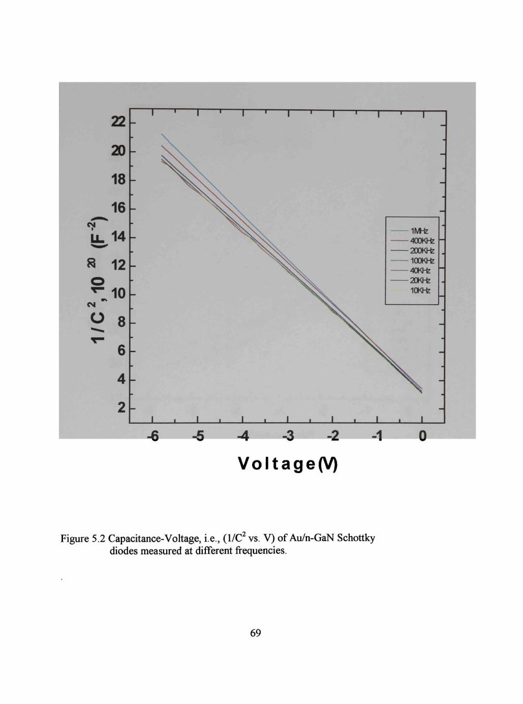
Voltage(V)
Figure 5.2 Capacitance-Vohage, i.e., (1/C^ vs. V) of Au/n-GaN Schottky diodes measured at different frequencies.
69

Voltage (V)
Figure 5.3 Capacitance-Voltage measurements of Ni/n-GaN using the one-mask process for different frequencies.
70
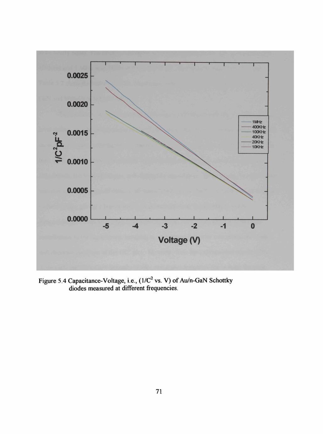
Figure 5.4 Capacitance-Voltage, i.e., (1/C^ vs. V) of Au/n-GaN Schottky diodes measured at different frequencies.
71
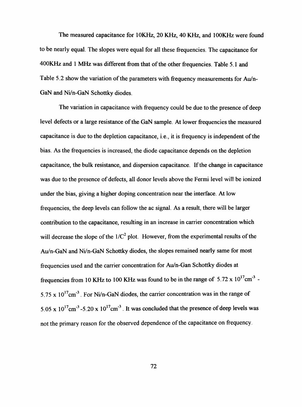
The measured capacitance for lOKHz, 20 KHz, 40 KHz, and lOOKHz were found
to be nearly equal. The slopes were equal for all these frequencies. The capacitance for
400KHz and 1 MHz was different from that of the other frequencies. Table 5.1 and
Table 5.2 show the variation of the parameters with frequency measurements for Au/n-
GaN and Ni/n-GaN Schottky diodes.
The variation in capacitance with frequency could be due to the presence of deep
level defects or a large resistance of the GaN sample. At lower frequencies the measured
capacitance is due to the depletion capacitance, i.e., it is frequency is independent of the
bias. As the frequencies is increased, the diode capacitance depends on the depletion
capacitance, the bulk resistance, and dispersion capacitance. If the change in capacitance
was due to the presence of defects, all donor levels above the Fermi level will be ionized
under the bias, giving a higher doping concentration near the interface. At low
frequencies, the deep levels can follow the ac signal. As a result, there will be larger
contribution to the capacitance, resulting in an increase in carrier concentration which
will decrease the slope of the 1/C^ plot. However, from the experimental results of the
Au/n-GaN and Ni/n-GaN Schottky diodes, the slopes remained nearly same for most
frequencies used and the carrier concentration for Au/n-Gan Schottky diodes at
frequencies from 10 KHz to 100 KHz was found to be in the range of 5.72 x lO^^cm' -
5.75 X lO^^cm" . For Ni/n-GaN diodes, the carrier concentration was in the range of
5.05 X lO^ cm" -5.20 x lO^^cm" . It was concluded that the presence of deep levels was
not the primary reason for the observed dependence of the capacitance on frequency.
72
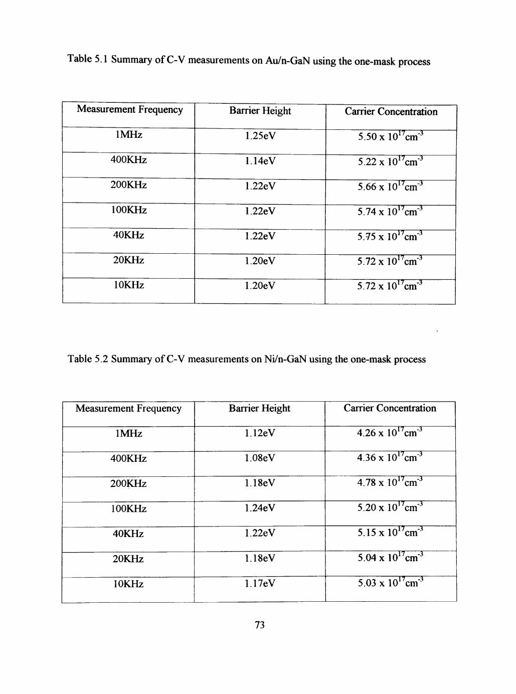
Table 5.1 Summary of C-V measurements on Au/n-GaN using the one-mask process
Measurement Frequency
IMHz
400KHZ
200KHZ
lOOKHz
40KHz
20KHz
lOKHz
Barrier Height
1.25eV
1.14eV
1.22eV
1.22eV
1.22eV
1.20eV
1.20eV
Carrier Concentration
5.50xl0^^cm'^
5.22 X lO^^cm'
5.66xl0^^cm'^
5.74xl0'^cm''
5.75 X lO^ cm'
5.72xl0'^cm-'
5.72 X lO' cm'
Table 5.2 Summary of C-V measurements on Ni/n-GaN using the one-mask process
Measurement Frequency
IMHz
400KHZ
200KHZ
lOOKHz
40KHz
20KHz
lOKHz
Barrier Height
1.12eV
1.08eV
1.18eV
1.24eV
1.22eV
1.18eV
1.17eV
Carrier Concentration
4.26 X lO'^cm'
4.36 X lO' cm'
4.78 X lO^^cm'
5.20xlO'^cm'^
5.15xlO'^cm"'
5.04 X lO^^cm'
5.03 X lO^^cm'
73
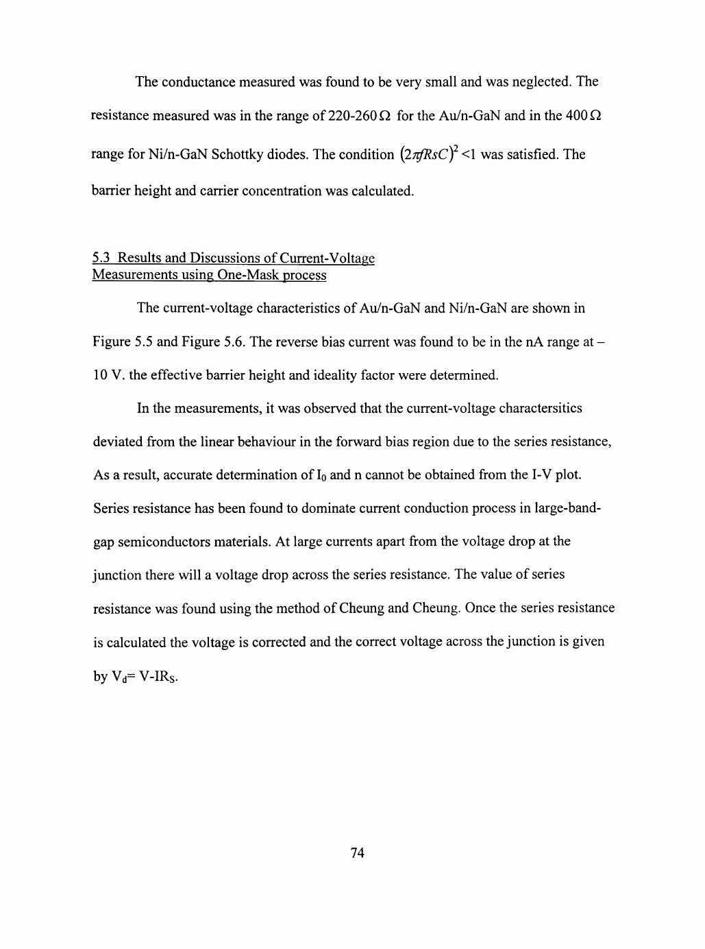
The conductance measured was found to be very small and was neglected. The
resistance measured was in the range of 220-260 Q for the Au/n-GaN and in the 400 Q.
range for Ni/n-GaN Schottky diodes. The condition {^TtfRsCY <1 was satisfied. The
barrier height and carrier concentration was calculated.
5.3 Results and Discussions of Current-Voltage Measurements using One-Mask process
The current-voltage characteristics of Au/n-GaN and Ni/n-GaN are shown in
Figure 5.5 and Figure 5.6. The reverse bias current was found to be in the nA range at -
10 V. the effective barrier height and ideality factor were determined.
In the measurements, it was observed that the current-voltage charactersitics
deviated from the linear behaviour in the forward bias region due to the series resistance.
As a result, accurate determination of IQ and n cannot be obtained from the I-V plot.
Series resistance has been found to dominate current conduction process in large-band-
gap semiconductors materials. At large currents apart from the voltage drop at the
junction there will a voltage drop across the series resistance. The value of series
resistance was found using the method of Cheung and Cheung. Once the series resistance
is calculated the voltage is corrected and the correct voltage across the junction is given
by Vd= V-IRs.
74
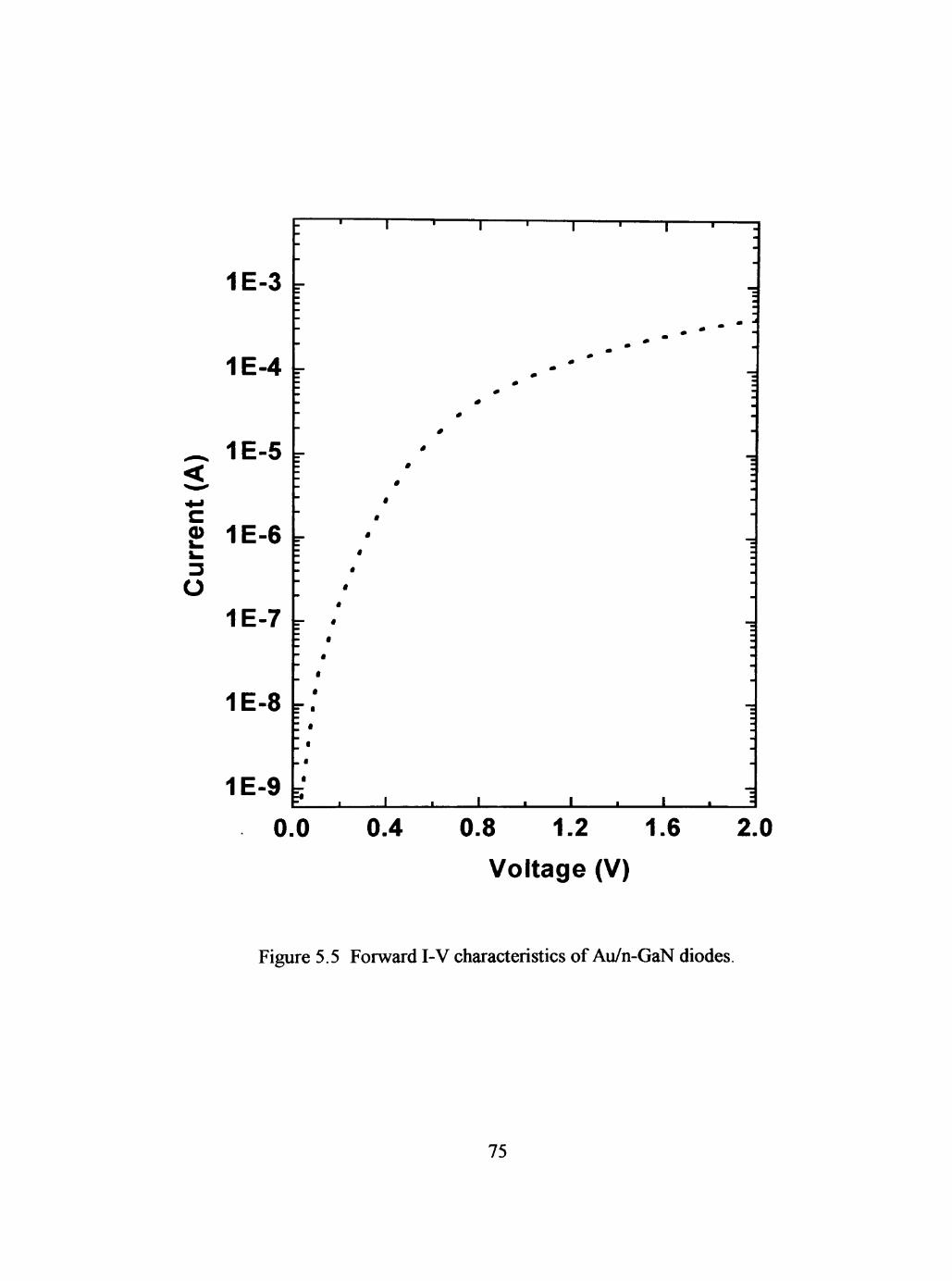
1E-3 ^
1E-4 .
^ 1E-5 <
g> 1E-6
o 1E-7 ^
1E.8 r
1E-9 =;•
-
—
-"
^ " -m
---
2 2 •
-"
; • ™
" -•
:-•
" " 1
i
i
t
U
1
• t
« «
• •
t
1
« •
•
1
«
#
T
tf
1
tf
1
tf
1
* «
- I
• m
1
«
1
« «
f
1
«
1
« •
" • •<
*
a
I •
^ --
^ H -
--
I •• a
. -•
_ B
-_ .
;
-
I
0.0 0.4 0.8 1.2 1.6
Voltage (V)
2.0
Figure 5.5 Forward I-V characteristics of Au/n-GaN diodes.
75

04 as 1.2
NADHage(V)
1.6 20
Figure 5.6 Forward I-V characteristics of Ni/n-GaN diodes using the one-mask process.
76
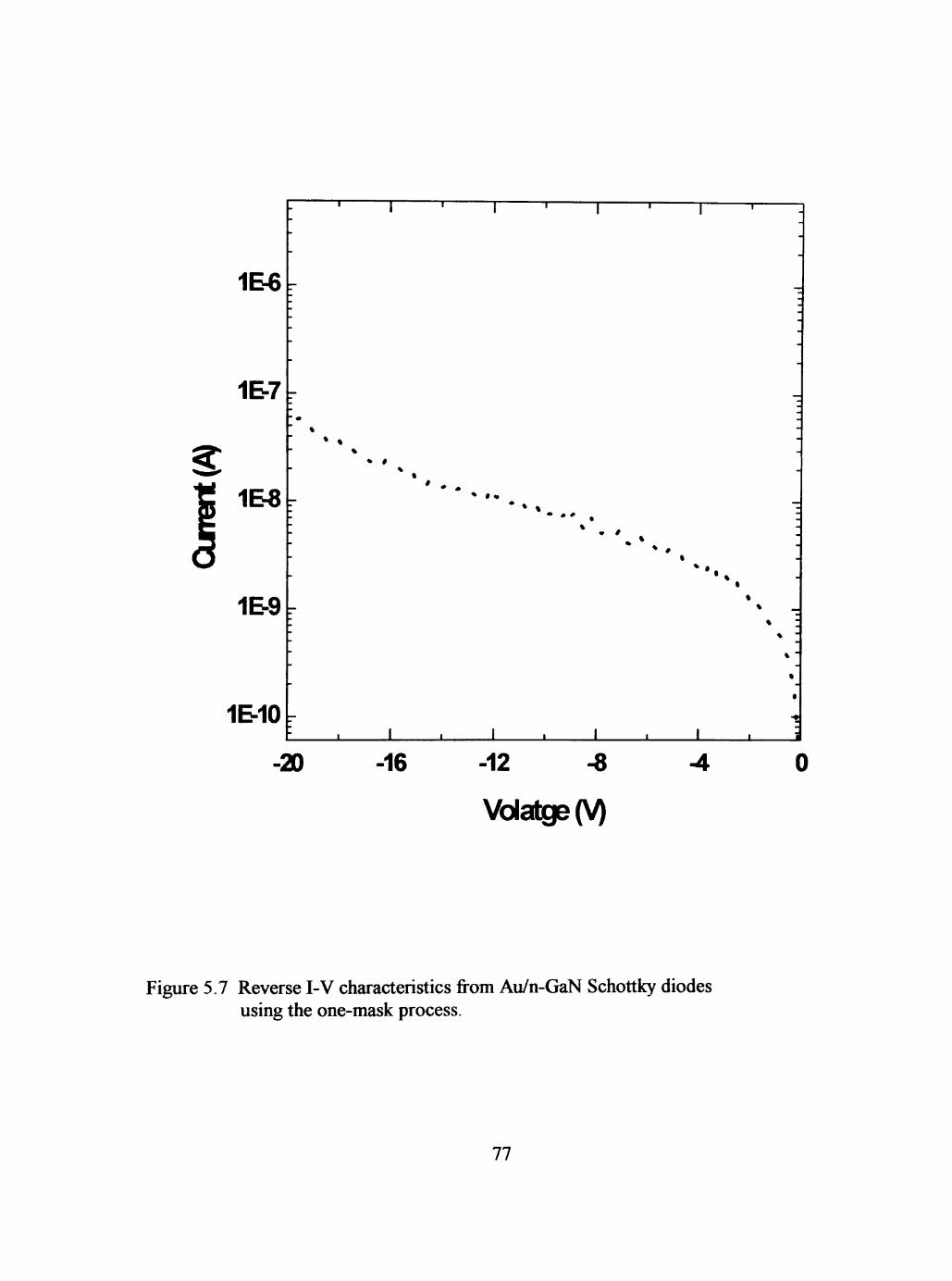
1E€
1&7r
1B8r
1&9r
1E-10
-20 -16 -12
Volatge(V)
Figure 5.7 Reverse I-V characteristics from Au/n-GaN Schottky diodes using the one-mask process.
77
1E5.
1E6
^
1E-7
1E6
1B9
1E-10
T—1
1 [III
1 1 T—1
1 [1
11 1
1 1
• 1
1 1
Iniii 1
• ' • • • • •
•
• •
• • • -
• 3
[ % -
•
* • _
• •
_ J
: ] • a
: . 1 . 1 . 1 . 1 . 1 1 :
^ -25 -20 -15 -10
Voltage (\0
Figure 5.8 Reverse I-V characteristics from Ni/n-GaN Schottky diodes using the one-mask process
78
A plot of the natural log of current versus forward bias voltage for small forward
currents are plotted, the family of ln(I) versus Vd plot is investigated. The curves are
linear over the entire vohage range. Accurate values of the ideality factor n. Is and barrier
height are calculated. The results are summarized in Table 5.3.
Table 5.3 Summary of the characteristics of the Schottky barriers from I-V measurements using one-mask
Metal
Au/n-GaN
Ni/n-GaN
Barrier height
0.9eV
0.901eV
Ideality factor
1.01
1.2
In the measurements, the value of the series resistance has been found to be 350-
550 Q. The large series resistance is attributed to the large spacing between the contacts.
The values of n calculated are in general agreement with those reported for Schottky
diodes on n-GaN samples. "^ The ideality factor of neariy unity in one diode indicated
the current flow by thermionics in the small forward bias region. In the measurements,
the ideality factor was found to range between 1 OleV - 2.4 eV for some diodes. Higher
values of ideality factor indicate the nonideal behaviour of the diodes. It suggests that
apart from thermionic, other ttansport mechanism may be present in the diode.
The reverse breakdown voltage for Au and Ni Schottky diodes were measured.
The range was between -lOV and -30V for Au/n-GaN and in the range of-lOV and -40
V for Ni/n-GaN diodes. The reverse bias current was found to be ~90nA for -20V for
79
Ni/nGaN and ~60nA for Au/n-GaN. There was a variation in the breakdown voltage for
different diodes. This variation was associated with the non-uniformities in the electron
concentration of the sample. However, once the reverse bias vohage exceeded the range,
subsequent measurements showed degradation of the reverse characteristics of the
diodes. The reverse characteristics were not investigated in detail because the diodes
were not passivated by a mesa etch or similar measure.
The barrier height is calculated using the theoretical value of the Richardson
constant. The electron affinity 2^ of the semiconductor is defined as the energy difference
between an electron at the bottom of the conduction band and an electron at the vacuum
level. It is related to the work fimction of the metal and the barrier height by
^s-^m~ ^Bn • Due to the charges present at the junction, this relation is only true for
the ideal case. Taking the value of the barrier height from the measurements, the electron
affinity is calculated to be 4.2eV for Au/n-GaN and 4.249 eV for Ni/n-GaN
The barrier height obtained from CV is larger than that from I-V . The value of
the barrier height from the capacitance-voltage measurements are found to be 0.2 eV
more than that measured from the I-V characteristics. This behavior is attributed to the
fact that the transport mechanism in these diodes is not purely due to thermionic
emmisions alone, other transport mechanism are also present in the diodes. The barrier
height from the I-V measurements are voltage or electric field sensitive while that
measured from C-V are not. The difference between the barrier height can also be due to
the presence of a native oxide layer at the metal semiconductor interface. Almost all
Schottky diodes have a thin oxide layer or insulatmg layer. These layers contribute to the
80
larger value of Vo and thus, give a higher value for the barrier height. An other possible
reason for the increased barrier height can also be due to the deep level. If the deep levels
emit carriers to the conduction band, it can affect the capacitance measurements. Since
the capacitance-vohage measurements signified that the deep levels are not so prominent
in the measurements, this reason was not taken. According to Werner and Guttler, "^
spatial inhomogeneities at the metal-semiconductor interface of the Schottky contacts
also can contribute to the difference in the barrier height determined from the I-V and C-
V measurements.
5.4 Results and Discussions of Capacitance-Voltage Measurements using Two-Mask process
During the measurements it was observed that the sample was not uniform with
regard to the concentration of electrons. It ranged from 3x10 cm' to 10 cm" .
The areas where Au contacts were made were regions which showed more variation in
the distribution of electron concentration than the areas where the Ni contacts were made.
This section describes the various capacitance voltage measurements done on the Au/n-
GaN and N-/n-GaN schottky diodes fabricated using two masks. Figure 5.9 and Figure
5.10 shows the capacitance-vohage curves for Au/n-GaN Schottky contacts where a
carrier concentration of 10^ cm' and 10^^ cm' were observed. The barrier height and
carrier concentrations for these ranges are given in Table 5.4 and Table 5.5, respectively.
The capacitance-Vohage measurements for Ni/n-GaN is shown in Figure 5.11 and
the barrier height and carrier concentrations are summarized in Table 5.6.
81
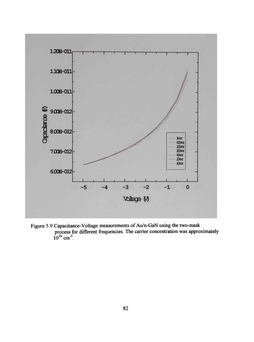
Figure 5.9 Capacitance-Vohage measurements of Au/n-GraN using the two-mask process for different frequencies. The carrier concentration was approximately 10'*cm-l
82

Figure 5.10 Capacitance-Vohage measurements of Au/n-GaN using the two mask process for different frequencies. The carrier concentration was approximately 10 cm' -3
83
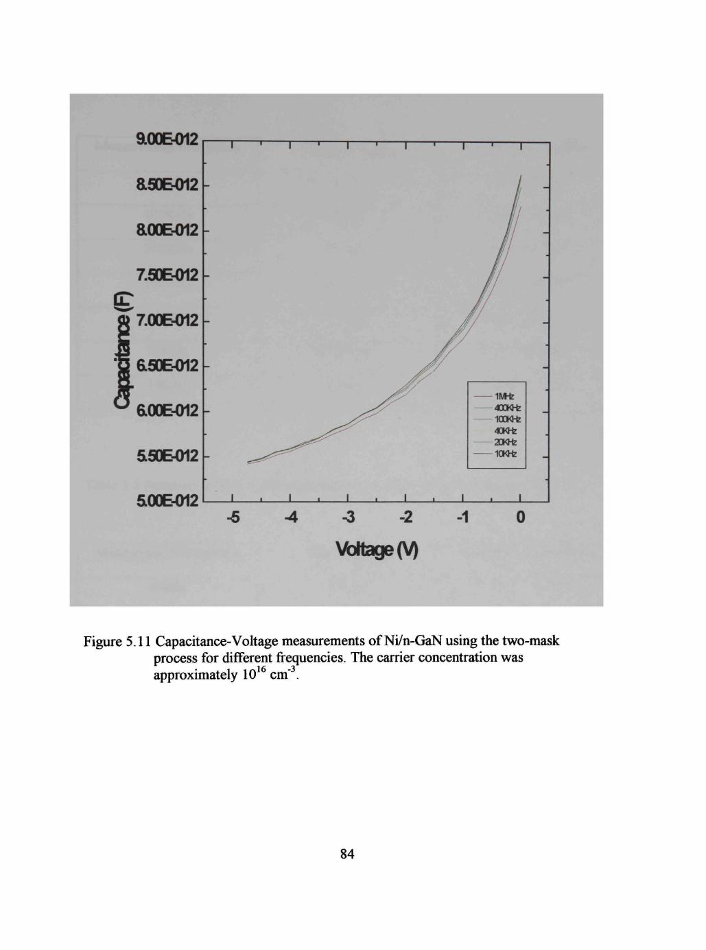
Figure 5.11 Capacitance-Voltage measurements of Ni/n-GaN using the two-mask process for different frequencies. The carrier concentration was approximately 10 ^ cm' .
84

Table 5.4 Summary of C-V measurements on Au/n-GaN using two-mask process
Measurement Frequency
IMHz
400KHZ
200KHz
lOOKHz
40KHz
20KHz
lOKHz
Barrier Height
2.18eV
2.05eV
2.04eV
2.02eV
1.96eV
2.01eV
2.02eV
Carrier Concentration
3.71 x lO' cm'
3.64xl0'^cm'^
3.66xl0^^cm'^
3.62xl0*^cm'^
3.60xl0^^cm'^
3.63 x lO^ cm'
3.41 x lO^ cm"
Table 5.5 Summary of C-V measurements on Au/n-GaN using two-mask process
Measurement Frequency
IMHz
400KHZ
200KHz
lOOKHz
Barrier Height
1.28eV
1.08eV
1.19eV
1.20eV
Carrier Concentration
5.628 x lO'^cm''
4.36xl0'^cm'^
5.75 X lO' cm'
5.85 x lO^^cm'
85
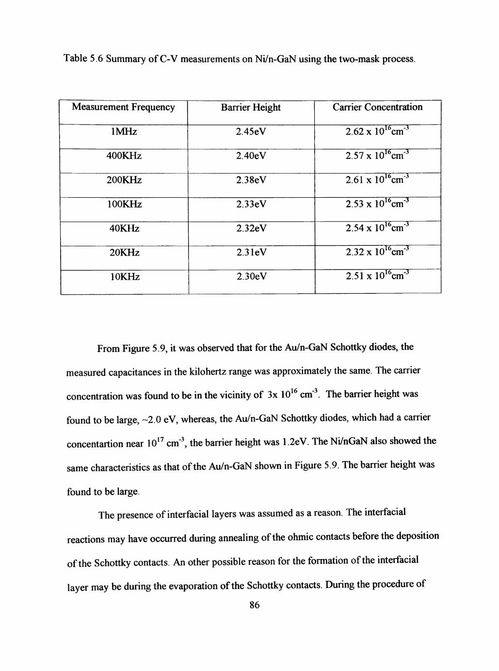
Table 5.6 Summary of C-V measurements on Ni/n-GaN using the two-mask process.
Measurement Frequency
IMHz
400KHZ
200KHZ
lOOKHz
40KHz
20KHz
lOKHz
Barrier Height
2.45eV
2.40eV
2.38eV
2.33eV
2.32eV
2.3 leV
2.30eV
Carrier Concentration
2.62xl0^^cm'^
2.57xl0'''cm'^
2.61 X lO^ cm'
2.53 X lO' 'cm'
2.54 X lO' 'cm'
2.32 X lO' 'cm'
2.51 X lO' 'cm'
From Figure 5.9, it was observed that for the Au/n-GaN Schottky diodes, the
measured capacitances in the kilohertz range was approximately the same. The carrier
concentration was found to be in the vicinity of 3x 10 ^ cm'l The barrier height was
found to be large, -2.0 eV, whereas, the Au/n-GaN Schottky diodes, which had a carrier
concentartion near 10^ cm'^ the barrier height was 1.2eV. The Ni/nGaN also showed the
same characteristics as that of the Au/n-GaN shown in Figure 5.9. The barrier height was
found to be large.
The presence of interfacial layers was assumed as a reason. The interfacial
reactions may have occurred during annealing of the ohmic contacts before the deposition
of the Schottky contacts. An other possible reason for the formation of the interfacial
layer may be during the evaporation of the Schottky contacts. During the procedure of
86
evacuation of the evaporation chamber, the oil vapor from the oil-pumped roughing
systems might have condensed on the semiconductor before the metal was deposited,
resuhing in the formation of an interfacial layer. The interfacial layer has an effect on the
capacitance. The layer modifies the dependence of charge in the depletion region on the
bias vohage. The capacitance of the depletion region is in series with that of the
interfacial layer. Thus, the capacitance is a complicated parameter.
The interfacial layer may have a different work fimction, which is responsible for
the increase in barrier heights. The effect of an interfacial layer on capacitance has been
analyized by Cowley, the analysis assumes that the interfacial layer is thin. The
interfacial sates that may exist at the interfacial insulator/semiconductor interface are
filled or emptied by the tunneling of electrons from the metal contact. Under such
conditions, the interface states need not be taken into account in calculating the
capacitance. The slope of such states remained straight. From the measurements of the
Au/n-GaN with a concentration of 10 cm', it was observed that the 1/C versus V plot
remained linear.
When an interface layer is present, the flat vohage is modified as
Vft-Oto-^ + ^1 IrT \/f I^T\/2
'2 kT y2 0
+—*-V ^) "^
where VA, is the flatband vohage in the presence of a insulating layer, ^ is the separation
between the Fermi level and the conduction band minimum, 0^^ is the zero-bias barrier
height, Vdo the band bending at zero bias, and 0^ = la^q y^ . The interfacial layer is
characterized by a parameter a - 5s l^s^ + qSDg), where S is the thickness of the layer,
87
£s and £•, are the permittivity of the semiconductor and the interfacial layer, Ds is the
interface state density. The barrier height increased due to the presence of the interfacial
layer.
In the observation, h was found that some of the diodes the interfacial layer was
so thick that the graph of C' vs V was not linear. It was concluded that the thickness of
the interfacial layer was also not uniform in the sample.
5.5 Results and Discussions of Current-Voltage Measurements using Two-Mask process
The forward current-vohage characteristics of Au/n-GaN and Ni/n-GaN are
shown in Figure 5.12 and Figure 5.13, respectively. Figure 5.14 and Figure 5.15 shows
the reverse current-voltage characteristics of the Au/n-GaN and Ni/n-GaN Schottky
diodes. The effective barrier height and ideality factor were determined.
In the measurements, it was observed that the current-voltage characteristics
deviated from the linear behaviour in the forward bias region due to the series resistance,
similar to the condition in the one mask process. As a result, accurate determination of lo
and n cannot be obtained from the I-V plot. The series resistance was calculated and the
vohage was corrected and the corrected vohage across the junction is given by Vd= V-
IRs.
A plot of the natural log of current versus forward bias vohage for small forward
currents have been plotted. The family of ln(I) vs Vd plot was investigated. The curves
are linear over the entire voltage range. Accurate value of ideality factor n. Is and barrier
height were calculated. The results are summarized in Table 5.7
88

1E4
1E«.
1E€.
1E-7
1E6.
^E9r.
1
'•
"•
•'
•
-
0
0
\ 0
0
0
0
* 1
1 > 1 • 1 \ . .V ' T • • •
• * *
/ 0
0
0
0
0
0
0
0
1 . 1 . 1 . 1 .
-i 1
. 1
1 ll
lll
l_.J
1
1
1 1
llll
l 1
1 1 ll
lll
-
-1
1
1 1
1 ll
ll
[ill 1 1
1
--
-;
04 08 12
Voltage (V)
1.6 20
Figure 5.12 Forward I-V characteristics of Au/n-GaN diodes using the two-mask process.
89
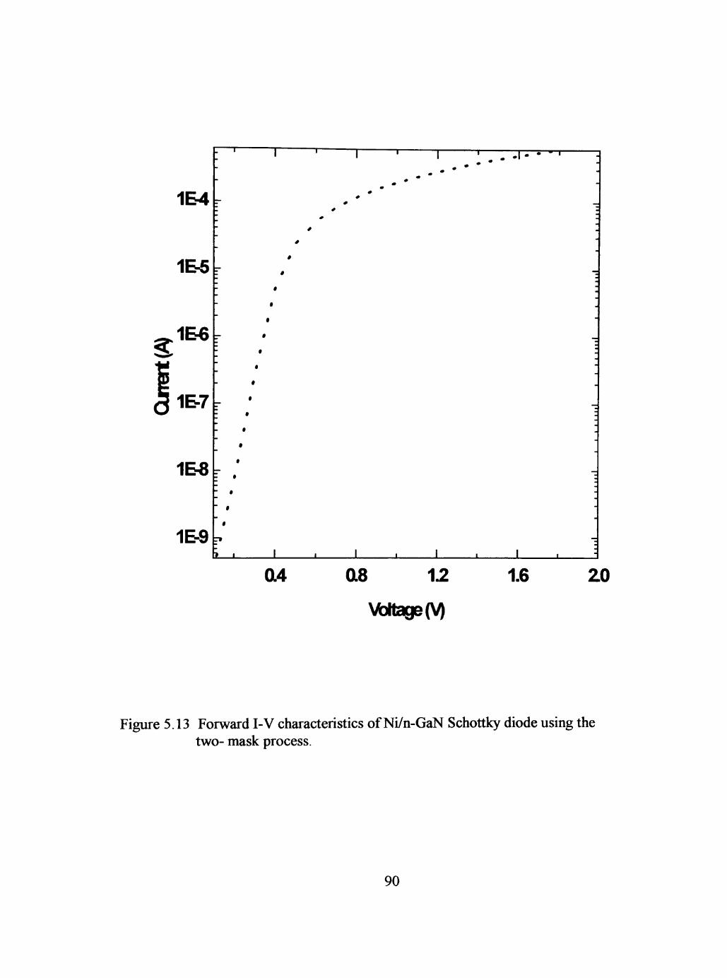
1E4
1B6.
1B6
1B-7.
1E«
l E Q .
-" •
^ z . -
lllll
-
"
r
-
_
-
~ -
-
-
~
4
-" 0
0
r»
?
' 1
0
0
0
$
$
0
0
0
0
0
0
0
0
0
*
1
* »
1
^
1
» *
1
«
1
«
— r
•
,
# «
1 . •
1
• •
T -
•
1
« • .1
1
• " • - ' - T —
,
_
•
. z --•
;
--
_ ;
-
-
^ ; "
-
; . --
-:
-
04 08 ^2
\A)ltage(\0
1.6 20
Figure 5.13 Forward I-V characteristics of Ni/n-GaN Schottky diode using the two- mask process.
90
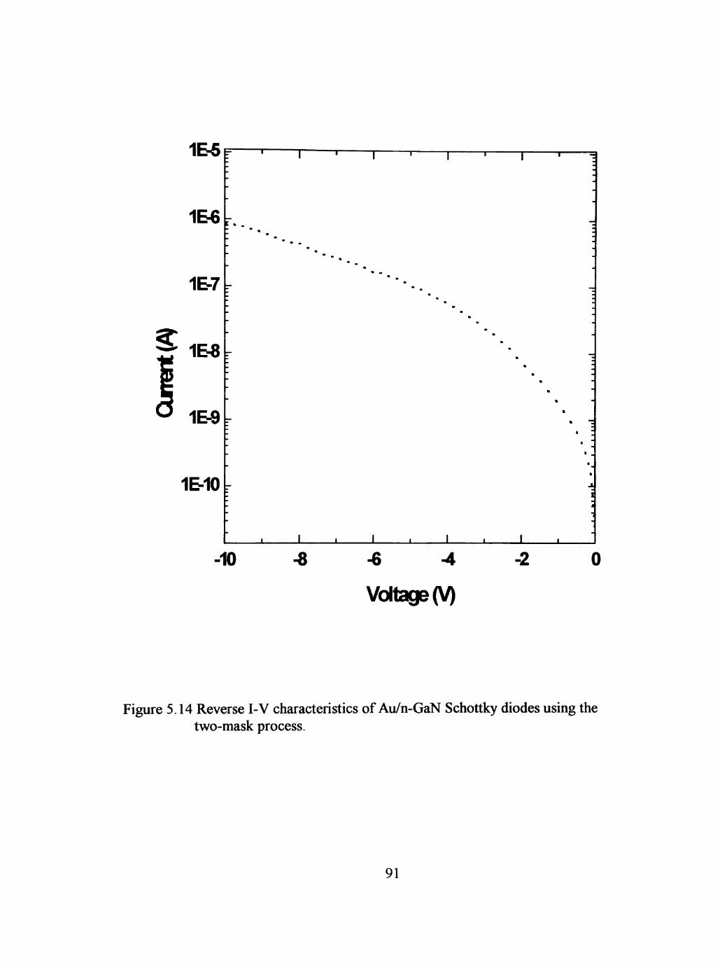
I C Q
1E«
1E-7
1E8
1E8
1E-10
1 1
1 iiiii|
c . . -
_ • • •
m
' m m
m
• •
• * • -
• " m "
- ' I 1
• •
: i
1 . 1 . 1 . 1 . •
-10 -8
Volt£ge(V)
-2
Figure 5.14 Reverse I-V characteristics of Au/n-GaN Schottky diodes using the two-mask process.
91
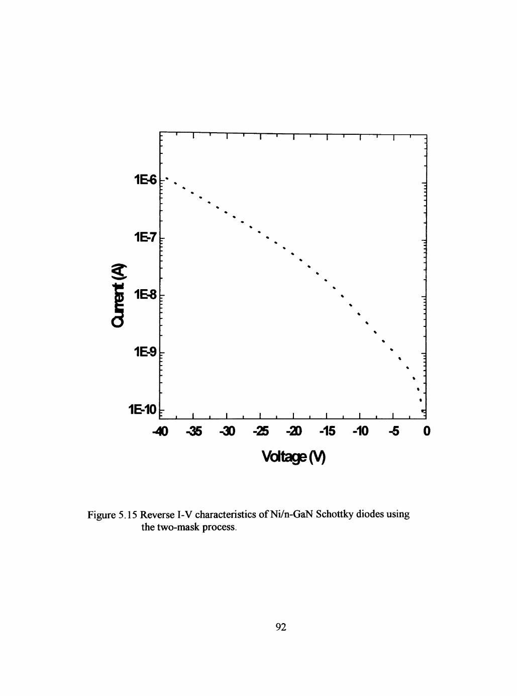
1E6
1&7
1E8
1EQ
E-10
_•
!
-
— I —
« «
_J
1 > 1 1 1 1 1 r 1 1 1 ,
«
* %
* «
\
i , 1 . 1 . 1 . 1 1 1 .
1 ' -
-
; --
-
-
-
-
-
-
•
K 1 1 -
- « - ^ -30 -25 -20 -15 -10
Voltage (V)
Figure 5.15 Reverse I-V characteristics of Ni/n-GaN Schottky diodes using the two-mask process.
92
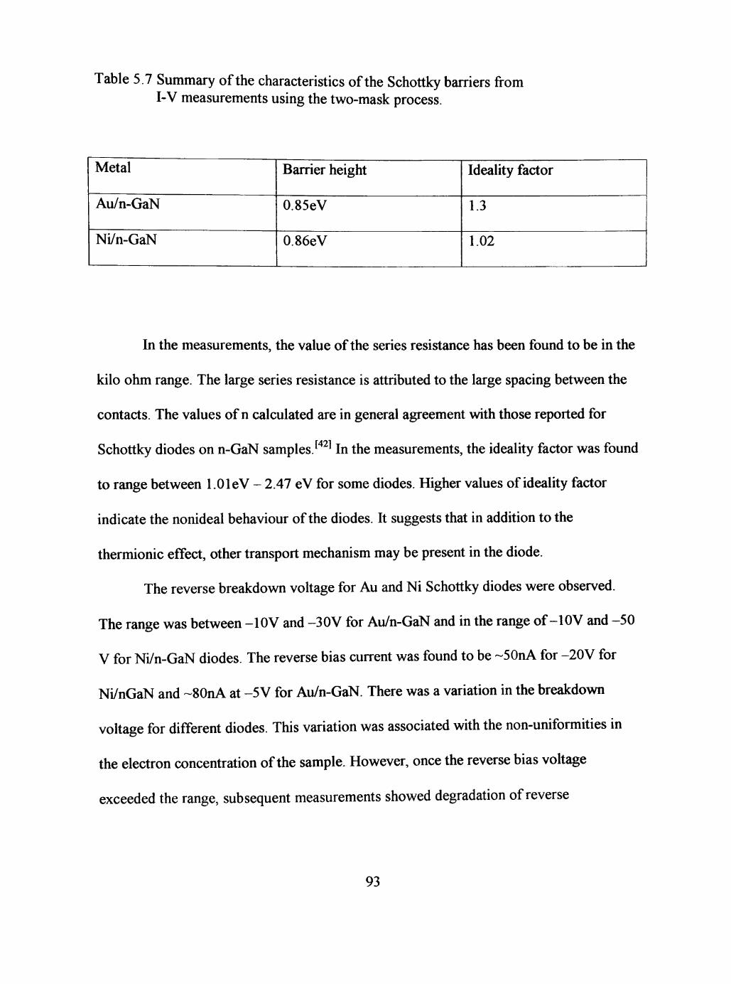
Table 5.7 Summary of the characteristics of the Schottky barriers from I-V measurements using the two-mask process.
Metal
Au/n-GaN
Ni/n-GaN
Barrier height
0.85eV
0.86eV
Ideality factor
1.3
1.02
In the measurements, the value of the series resistance has been found to be in the
kilo ohm range. The large series resistance is attributed to the large spacing between the
contacts. The values of n calculated are in general agreement with those reported for
Schottky diodes on n-GaN samples. "^ In the measurements, the ideality factor was found
to range between 1.OleV - 2.47 eV for some diodes. Higher values of ideality factor
indicate the nonideal behaviour of the diodes. It suggests that in addition to the
thermionic effect, other transport mechanism may be present in the diode.
The reverse breakdovm vohage for Au and Ni Schottky diodes were observed.
The range was between -lOV and -30V for Au/n-GaN and in the range of-lOV and -50
V for Ni/n-GaN diodes. The reverse bias current was found to be ~50nA for -20V for
Ni/nGaN and ~80nA at -5 V for Au/n-GaN. There was a variation in the breakdown
voltage for different diodes. This variation was associated with the non-uniformities in
the electron concentration of the sample. However, once the reverse bias voltage
exceeded the range, subsequent measurements showed degradation of reverse
93
characteristics of the diodes. The reverse characteristics were not investigated in detail
because the diodes were not passivated by a mesa etch, or similar measure.
The barrier height is calculated using the theoretical value of Richardson constant.
The barrier height obtained from CV is larger than that from I-V.
5.6 Conclusion
In summary, two different processing techniques for the fabrication of Schottky
diodes have been compared. The one-mask process have given better results in terms of
barrier height. A barrier height of 1.2 eV for Au/n-GaN and 1.18 eV for Ni/n-GaN is
obtained using this method and is better than the results published so far for Au and Ni.
The results obtained from the two-mask process was not very good when compared with
that of one mask, due to the possible formation of an interfacial layer between the contact
and the semiconductor. As a result, the barrier height increased. It was also observed that
the interfacial layer was not uniform giving rise to some good diodes with a barrier height
of 1.2eV for Au/n-GaN Schottky diodes.
94

CHAPTER VI
CONCLUSIONS
Gallium Nitride (GaN) is one of the few instances in the history of
semiconductors where the device applications have even come before the properties of
the semiconductor were understood completely. The technology of GaN is progressing
quhe rapidly which suggests that the electronic potential of III-V based nitrides can be
realized; GaN based electronics will be a reality.
The application of GaN includes various fields like displays, data storage, UV
detectors, high power microwave applications, new sensor technologies. A recent report
of an implanted GaN FET suggests that implanted IC technology is possible. As a better
understanding of the properties of this material evolve, more rapid development in the
device applications will be seen. The interest in GaN has exploded in the past few years,
leading some to predict that GaN will eventually become a very important semiconductor
next to Si and GaAs.
The research done in this thesis promises good Schottky and ohmic contacts to n-
type GaN semiconductor. The multilayer (Ti/Al/Ti/Au) formed good ohmic contact to n-
type GaN. The Au and Ni proved to be good Schottky contacts.
GaN device development has recently emphasized GaN based FETs. Good
Schottky contacts are a prerequishe. The processing technique for the fabrication of the
Schottky diodes and the metal semiconductor contacts used in this work are now used for
the fabrication of FETs in the lab.
95
REFERENCES
1 EH. Rhoderick, "Metal Semiconductor Contacts :'C\aiQndon Press, Oxford (1978).
2. Hadis Morkoc, ""Nitride Semiconductors and Devices.'' Springer New York (1998).
3. Shuji Nakamura and Gerhard Fasol," The Blue Laser Diode.'' Springer New York (1997).
4. Ralph Williams, ""Modern GaAs Processing Methods," Aetech House (1990).
5. R. Juza, and H. Hahn, Z. Anorg. Allgem. Chem 234, 282 (1938); and 244,133 (1940).
6. W.C.Johnson, j.B.Parsons, M.C. Crew: J.Phys.Chem .234 ,2651 (1993)
7. H.Grimmeiss, and Z.H-Koelmans, Nature 14a, 264 (1959)
8. H.P.Maruska, and J.J.Tietjen, Appl. Phys. Lett. 15, 367 (1969)
9. S. Yoshida, S. Misawa, and S.Gonda, Appl. Phys. Lett. 42, 427 (1983)
10. J.I.Pankove, in GaN and Related Materials, edited by S.J.Pearton, Gordon and Breach, New York. (1997), pp. 1-9
11. J.I.Pankove, E.A. Miller, and J.E.Berkeyheiser, J.Lumin. 5, 84 (1972); J.IPankove, E.A.MiHer, and J.E.Berkeyheiser, RCA Rev . 32, 383 (1971); J.I. pankove, M.T.Duffy, E.A. Miller, and J.E. Berkeyheiser, J.Lumin. 8, 89 (1972).
12. J.I.Pankove and H.E.P.Schade, appl. Phys. Lett. 25, 53 (1974).
13. M.T.Dufry, C.C.Wang, G.d. O'clock, S.HMcFarlane, andP.Z.zanzucchi, JElectron. Mater2., 359(1973).
14. H.Amano, I.Akasaki, T.Kozawa, K.Hiramatsu, N.Sawak, K.Ikeda, and Y.Ishi, J.Lumin. 40-41, 121 (1998)
15. I.Akasaki, H.Amano, Tech. Dig. Int. Electron Devices Meet. 96,231 (1996).
16. I.Akasaki, H.Amano, and I.Suemune, Inst.Phys. Conf. Ser. 142, 7 (1996).
96
17. I. Akasaki and H. Amano, in GaN, edited by J.I.Pankove and T.D.Moustakas. Academic, New York. (1998), Vol. 1, pp 459-72.
18. H.Amano, N.Sawaki, I.Akasaki, and Y.Toyoda, Appl. Phys. Lett. 48,353 (1986); H.Amano, I.Akasaki, T.Kozawa, K.Hiramatsu, N.Sawaki, K.Ikeda, and Y.Ishii, J.Lumin. 40&41, 121 (1988); H.Amano, M.kito,K.Hiramatsu, and I.Akasaki, Jpn. J. appl. Phys., Part 2 28, L2112 (1989
19. S.Nakamura and G.Fasol, The Blue Laser Diodes. Springer, Heidelberg. (1997).
20. J.Pearton, J.C.Zolper, RJ.Shul, and F.Ren, J. Appl. Phys.86, 1 (1999).
21. M. A.Khan, J.N.Kuznia, A.R. Bhattarai and D.T.Olson, "Metal semiconductor field effect transistor based on single crystal GaN," Appl. Phys. Lett. 62, 1786 (1993).
22. C.H.Qiu, J.I.Pankove, C.Rossington: In Nitride Based X-Ray Detectors, ed. By J.I. Pankove, T.D.Moustakas. Semiconductors and Semimetals, Vol. 50B (Academic, San Siedo 1998) pp. 1-24.
23. Robert F.Pierret, Semiconductor Device Fundamentals . Addison-Wesley PubHcation. (1996).
24. Li, Sheng S, Semiconductor Physical Electronics. Plenum Press, New York. (1993).
25 W.Kern, RCA Rev. 39, 278 (1978).
26 W.Kern, J.Electrochem. Soc. 137, 1887 (1990).
27 T.Ohmi, J.Electrochem. Soc. 143, 1957 (1996).
28 S.W.king, J.P. Bamak, MD.Bremser, K.M.Tracy, C.Ronning, RF.Davis and RJ.Nemanich. ""Cleaning of AIN and GaN surfaces." J.Appl Phys 84, 5248 (1998).
29 Stanley Wolf and Tauber, Richard N. ""Silicon Processing for The VLSI Era" Volume l,Lattice Press. (1986).
30. S.ANikishin, V.G.Antipov, S.Francoeur, N.N. Faleev, G.A.Seryogin, V.AElyukhin, H.Temkin, T.I.Prokofyeva, M.holtz, Akonkar, and S.Zollner, Appl. Phys. Lett. 75, 484 (1999).
31. S.ANikishin, N.N. Faleev, V.G.Antipov, S.Francoeur, L.Grave de Peraha, G.ASeryogin, H.Temkin, T.I.Prokofyeva, M.Holtz, and S.N.G.Chu. Appl. Phys.
97
Lett. 75, 2073 (1999).
32. M.Seon, T.I.Prokofyeva, M.Holtz, S.ANikishin, N.N. Faleev, and H.Temkin. Appl. Phys. Lett. 76, 1842 (2000),
33. J.D.Guo, M.S.Feng, R.J.Guo, F.M.Pan, and C.Y.Chang, Appl. Phys. Lett. 67, 2657(1995).
34. L.Wang, M.I.Nathan, T H.Lim, M. Akhan, and Q.Chen, Appl. Phys. Lett. 68, 1267 (1996).
35. S.N.Mohammad, Z.Fan, AE.Botchkarev, W.Kim, O.Aktas, ASalvador, and H.Morkov, Electron. Lett. 32, 598 (1996).
36. AT.Ping, AC.Schmitz, M.AKhan, andI.Adesida, Electron. Lett. 32, 68(1996).
37. Z.Z.Bandic, P.M.Bridger, E.C.Piquette, and T.C.McGiH, Appl. Phys. Lett. 74, 1266 (1999).
38. P.Hacke, T.Detchprohm, K.Hiramatsu, and N. Sawaki, Appl. Phys. Lett 63, 2676 (1993).
39. AC.Schmitz, AT.Ping, M.AKhan, J.W.Yang, and I.Adesida [Semicond. Sci. technol. (UK) Vol.11 (1996)p. 1464-7].
40. AC.Schmitz, A.T.Ping, M.A.Khan,Q.Chen, J.W.Yang, I.Adesida [J. Electron. Mater.(USA) vol.27 (1998)p.255-60.].
41. J.D.Guo, F.MPan, M.S.Feng, R.J.Guo,P.F.Chou, C.Y.Chang, J.Appl. Phys. (USA) 80, 1623-7 (1996).
42. Q.Z.Liu, l.S.Yu, F.Deng and S.S.Lay, Appl. Phys. Lett. 84, 881 (1998).
43. HS.Venugopalan and S.E. Mohney, Appl. Phys. Lett. 73, 1242 (1998).
44. J.K.Sheu and Y.K.Su. Appl. Phys. Lett. 72, 3317 (1998).
45. AC.Schmitz, AT.Ping, M.AKhan, Q.Chen, J.W.Yang, I.Adesida. Electron. Lett, 32 1832(1996).
46. Q.Z.Liu, L.S.Yu, S.S.Lau, J.M.Redwing, N.R.Perkins, T.D.Kuech. Appl. Phys. Lett. 70, 1275 (1997).
47. J.S.Forensi, T.D.Moustakas. Appl. Phys. Lett, 62, 2859 ,(1993).
98

48. H.S.Venugopalan and S.E. Mohney, Mater. Res. Soc. Symp. Proc, 512 (1998).
49. Z.Fan, S.Noor Mohammad, W.Kim, O.Aktas, E.Botchkarev, H.Morkoc. Appl. Phys. Lett. 68, 1672 (1996).
50. M.E.lin, Z.Ma, F.Y.Huang, Z.F.Fan, L.H.Allen, H.Morkoc. Appl. Phys. Lett. 64, 1003 (1994).
51. B.P.Luther, S.E.Mohney, T.N.Jackson, M.AKhan, Q.Chen, J.W.Yang, Appl. Phys. Lett. 70,57(1997).
52. Y.F.Wu et al. SoHd-state electron, 41, 165 (1997).
53. S.E.Mohney, B.P.Luther, S.d.Wolter, T.N.Jackson, R.f Kariicek Jr., R.S.Kem, t i l
Proc 4 Int. Conf On High Temperature Electronics Albuquerque, New Mexico, 134 (1998).
54. J.D.Guo, C.I.Lin, M.S.Feng, F.M.Pan, G.C.Chi, C.T.Lee, Appl. Phys. Lett. 68 235 (1996).
55. K.V.Vassilevski, M.G.Rastegaeva, AI.Babanin, I.P.Nikitina, V.ADmitriev. Mater. Sci.Eng, 43,292 (1997).
56. J.Burm, K.Chu, W.A.Davis, W.J.Schaff, L.F.Eastman, T.J.Eustis. Appl.Phys.Lett, 70,464 (1997).
57. B.P.Luther [PhD Dissertation, The Pennsylvania State University, 1997].
58. L.L.Smith et al.. Mater. Res. Soc. Symp. Proc, 449, 111055 (1997).
59. M.W.Cole et al, J.Appl.Phys, 80, 278,(1996).
60. AT.Ping, M.AKhan, I.Adesida. JElectron. Mater, 25,819(1996).
61. B.P.Luther, S.E.Mohney, J.M.DeLucca, RFkarlicek Jr., JElectron. Mater, 27 196, (1998).
62. M.RH.Khan, T.Detchprom, P.Hacke, K.Hiramatsu, and N.Sawaki, J.Phys. D 28, 1169(1995).
63. RSporken, C.Silien, F.Malengreau, K.Grigorov, R.Caudano, F.J.Sanchez, E.Calleja, E.Munoz, B.Beaumont, and Pierre Gibart, MRS Internet J.Nitride Semicond. Res .2, 23 (1997).
99

64. Jinwook B Burm, K.Chu, W.A.Davis, W.J.Schaff, L.F.Eastman, T.J.Eustis. Appl.Phys.Lett, 70,464 (1997).
65. M.W.Cole, F.Ren, and S.J.Pearton, J.Electrochem. Soc. 144, L275(1997); Appl. Phys. Lett. 71,3004(1997).
66. D.Qiao, L.S.Yu and S.S.Lau, Appl. Phys. Lett. 87, 801(2000).
67. X.A.Cao, H.Cho, and S.J.Pearton, Appl. Phys. Lett. 75, 232 (1999).
68. S.K.Cheung and N.W.Cheung, Appl. Phys. Lett. 49, 85 (1986).
69. James H.Edgar, Samuel Strite, Isamu Akasaki, Hirushi Amano and Christian Wetzel, "Properties, Processing and Applications of Gallium Nitride and related Semiconductors." INSPEC, London, United Kingdom. (1999).
70. Q.Chen, J.W.Wang, A.Osinsky, S.Gangopadhyay, B.Lim, M.Z.Anwar, and M.A.Khan, Appl. Phys. Lett. 70, 2277 (1997).
71. Dieter K.Schroder, ""Semiconductor Material and Device Characterization." John Wiley «fe Sons, Inc. (1998)
72. S.M.Sze, ""Physics of Semiconductor Devices. " John Wiely & Sons, New York. (1981).
73. J.H.Wemer and H.H.Guttler, J.Appl.Phys. 69, 1522 (1991).
100

PERMISSION TO COPY
In presenting this thesis in partial fulfillment of the requirements for a
master's degree at Texas Tech University or Texas Tech University Health Sciences
Center, I agree that the Library and my major department shall make it freely
available for research purposes. Permission to copy this thesis for scholarly
purposes may be granted by the Director of the Library or my major professor.
It is understood that any copying or publication of this thesis for financial gain
shall not be allowed without my further written permission and that any user
may be liable for copyright infringement.
Agree (Permission is granted.)
Student's Signature Date
Disagree (Permission is not granted.)
Student's Signature Date