
Multiphase Buck Converter Implementing Gallium Nitride ...
53
Multiphase Buck Converter Implementing Gallium Nitride Semiconductors Senior Project Final Report California Polytechnic State University, San Luis Obispo Electrical Engineering Department March 19, 2021 Faculty Advisor – Dr. Taufik Sponsor – Cisco Systems Kadin Stephens
Transcript of Multiphase Buck Converter Implementing Gallium Nitride ...

Multiphase Buck Converter
Implementing Gallium Nitride Semiconductors
Senior Project Final Report
California Polytechnic State University, San Luis Obispo
Electrical Engineering Department
March 19, 2021
Faculty Advisor – Dr. Taufik
Sponsor – Cisco Systems
Kadin Stephens

1
Contents
List of Figures
List of Tables
Abstract
Chapter 1. Introduction
Chapter 2. Background
Chapter 3. Design Requirements
Chapter 4. Design
Design Calculations
Chapter 5. Simulation Results and Analysis
OrCAD Simulation Setup
Buck Converter Timing and Driving Dead-Time
Inductor Current
Output Voltage
Power and Efficiency
Summary
Data Analysis
Chapter 6. Conclusion
References
A. Final Schematic
B. Project Schedule
C. Bill of Materials
D. Analysis of Senior Project Design
2
3
4
5
6
9
12
13
23
23
24
26
27
29
30
30
31
33
35
41
42
44

2
List of Figures
Figure 2-1: Standard Buck Converter Topology
Figure 2-2: Multiphase Buck Converter Topology
Figure 3-1: Level 0 Block Diagram
Figure 3-2: Level 1 Block Diagram
Figure 3-3: Level 2 Block Diagram
Figure 4-1: Phase One of 12-phase Buck Converter Schematic
Figure 4-2: Phase Two of 12-phase Buck Converter Schematic (repeated 10 more times)
Figure 4-3: Output Capacitor Mix Network
Figure 4-4: TPS536C7 Typical Application Controller Schematic
Figure 4-5: Current Sensing Circuitry for TPS536C7
Figure 4-6: OrCAD PCB Editor Board Layout
Figure 4-7: Fabricated Board (Top)
Figure 4-8: Fabricated Board (Bottom)
Figure 5-1: First Phase of Multiphase Buck Converter with Parameters
Figure 5-2: High-Side Gate Voltage Source Pulsing with 30° Phase Shift
Figure 5-3: High-Side FET (Green) and Low-Side FET (Red) Gate Driving
Figure 5-4: Individual Inductor Current
Figure 5-5: Average Inductor Current (Output Current)
Figure 5-6: Average Output Voltage
Figure 5-7: Output Voltage Ripple
Figure 5-8: Input (Green) and Output (Red) Power
7
7
10
10
11
17
18
18
20
21
22
22
23
24
25
26
27
27
28
28
29

3
List of Tables
Table 3-1: Marketing Requirements and Engineering Specifications
Table 4-1: Bill of Materials (Simulated Entry)
Table 5-1: Simulation Result Summary
12
16
30

4
Abstract
Efficiency and power loss contributions are two of the main concerns in power systems. This project
exerts the use of wide bandgap semiconductors, namely Gallium Nitride (GaN), and their benefit within a
Cisco Systems point-of-load converter. This project provides tools to assist researchers and practicing
engineers in performing further characterization, and implementation, of GaN devices. Silicon-based
Metal Oxide Semiconductor Field Effect (MOSFETs) transistors have prevailed in power conversion
applications for decades and are now considered an industry standard. Presently, the utilization of wide
bandgap semiconductors is an emerging, competitive technology, as they offer many major advantages
over the traditional silicon solutions. These advantages include increased power efficiency, higher thermal
conductivity, smaller form factors, the ability to increase current density, and much more. These
advantages motivated the implementation of wide bandgap solutions to create a new multiphase buck
converter design that transforms an unregulated input of 12V to 1V at 320A at the output. In low voltage
applications, wide bandgap semiconductors have proven to be useful. These semiconductors allow
innovators to push the envelope by exploring more efficient opportunities, like the opportunity explored
in this project, for power conversion applications.

5
Chapter 1: Introduction
Power electronics is the engineering study of converting electrical power from one form to
another [1]. In a power electronics system, we need to have at least two things: a source and a load. A
source generates power (i.e., a battery). A load consumes power (i.e., our computers, televisions, cell
phones, etc.). Power electronics is the circuitry of everything in between the source and the load. It is the
management of the power the load needs to be able to operate and carry on its functionalities. Also, in
power electronics, the main goal is efficiency. Efficiency in power electronics is the power that you see at
the output of the system divided by the power you see at the input of a system. The closer this numerical
value gets to 100%, or unity, we say the system is becoming more “efficient”.
There are different methods, or types, of power conversion to convert power from source to load.
There are DC – AC (Direct Current to Alternating Current), AC – DC, AC – AC, and DC – DC power
conversion tactics that are present everywhere in the world today. When one plugs in their phone into an
outlet to charge it, this is utilizing AC – DC power conversion since the source power from the outlet is
AC electricity while the battery being charged inside the phone is operating in DC electricity. People
often do not think about what type of power conversion they are using when they charge or use their
devices. They also probably do not think about the management system, the circuitry, that is being
utilized so they can use their electronic devices so seamlessly, but the reality of it is, is that some type of
power conversion is always taking place.
DC – DC converters are in our everyday devices. They are in our laptops, cell phones, digital
cameras, televisions – the list goes on and on. DC – DC conversion takes place when a higher voltage
needs to be converted down to a lower voltage or when a lower voltage needs to convert into a higher
voltage. A common power electronic circuit that accomplishes a high-to-low conversion is a Buck
Converter. Also, a Boost Converter is another system that performs a low-to-high conversion. There is

6
even a power converter that sits in between these two, using the same concepts of a Buck Converter and a
Boost Converter, and that is a Buck-Boost Converter.
These three DC-DC converters fall under the category of non-isolated DC – DC converters. Non-
isolated DC – DC converters are power converters that have a single circuit in which current can flow
between the input and the output. Isolated DC – DC power converters isolate the input from the output by
electrically and magnetically separating the circuit into two sections, preventing DC flow between the
input and output. This separation is commonly achieved by using a transformer [2]. Power converters can
be configured and added on to, to perform different functions and achieve different specifications, having
limitless applications in power electronics.
In this project, the focus is on the Buck converter. As previously mentioned, the Buck converter
provides the step-down function in DC-DC converter. As such, this converter is one of the most widely
used circuits in electrical systems since in most applications the source voltage is at a higher level than the
load voltage. In terms of the output power requirement, the Buck converter has been used in a wide
variety of applications ranging from milliwatts to kilowatts.
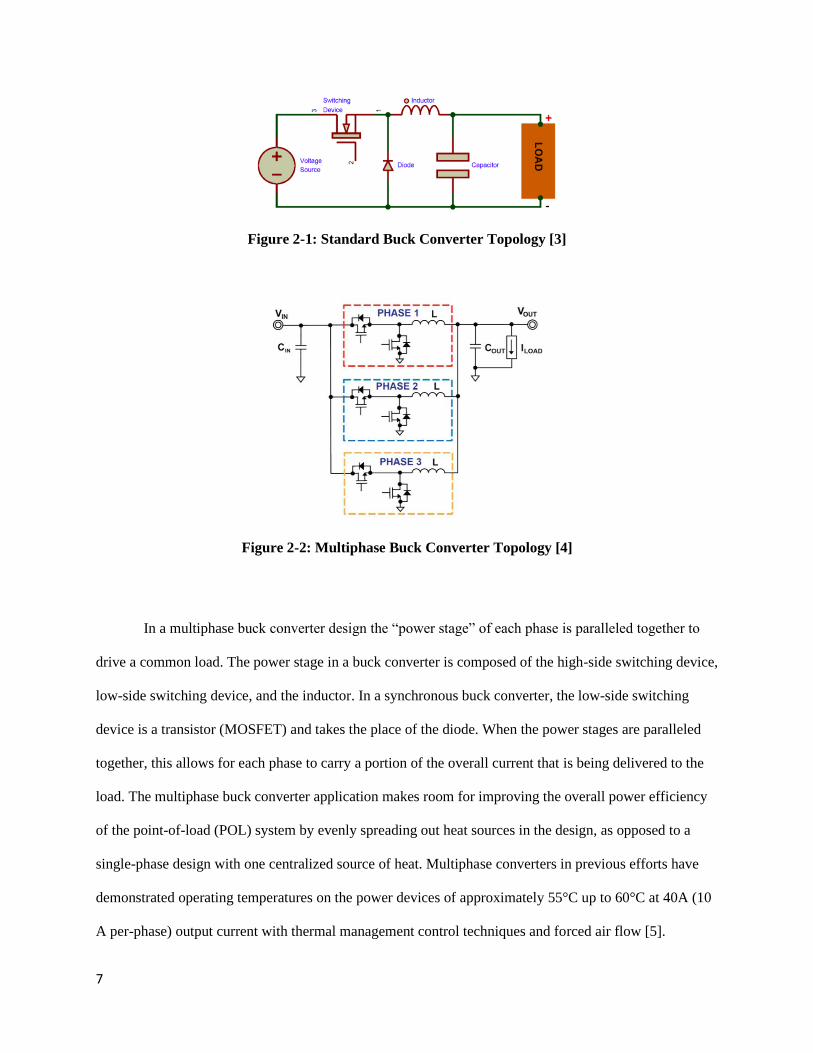
Chapter 2: Background
In a buck converter, there are three main electrical components: a switch, such as a MOSFET or
IGBT, a diode, and an inductor. There are different configurations of how buck converters look, but the
most common setup is shown in Figure 2-1. Through rapid switching, this design can achieve a voltage
step-down, from source to load, in an efficient manner. This design can be stacked to reach higher load
current specifications as well. The iterations of these stacked circuits, shown in Figure 2-2, are referred to
as “phases”.
7
Figure 2-1: Standard Buck Converter Topology [3]
Figure 2-2: Multiphase Buck Converter Topology [4]
In a multiphase buck converter design the “power stage” of each phase is paralleled together to
drive a common load. The power stage in a buck converter is composed of the high-side switching device,
low-side switching device, and the inductor. In a synchronous buck converter, the low-side switching
device is a transistor (MOSFET) and takes the place of the diode. When the power stages are paralleled
together, this allows for each phase to carry a portion of the overall current that is being delivered to the
load. The multiphase buck converter application makes room for improving the overall power efficiency
of the point-of-load (POL) system by evenly spreading out heat sources in the design, as opposed to a
single-phase design with one centralized source of heat. Multiphase converters in previous efforts have
demonstrated operating temperatures on the power devices of approximately 55°C up to 60°C at 40A (10
A per-phase) output current with thermal management control techniques and forced air flow [5].

8
In the growing technology industry, there is an increasing need for high efficiency and high
current POL converters. Multiphase buck converters also provide benefit when it comes to component
size reduction, which directly results in an increase in power density [6] and targets the industry’s high
demand for this increase in efficiency. Expanding to multiple phases also reduces the overall inductor
current ripple which improves the reliability of the devices as well as the load that is being driven by the
POL converter [7].
Some of today’s boards exceed 100A, while their output voltage is kept below 1V [8]. This trend
is seen in the increased usage of Application-Specific Integrated Circuits (ASICs). These ASICs require a
high current draw, are high performing, and have high power consumption. The most common solution to
accommodate the requirements of the high current draw at such a low voltage is, as mentioned, the
utilization of multiphase synchronous buck converters [9]. An example of high-power, multiphase buck
converter design that is currently in use and in mass production is the Cisco System JMAC. The JMAC is
a multiphase synchronous buck converter design (8 phases), capable of 320A at the output, rated at 1V.
At full load current draw, the JMAC is 93% power efficient. At half load, it is 89.2% power efficient [10].
Exploring an alternative semiconductor, rather than traditional Silicon, may have an increased positive
effect when it comes to increasing system efficiency.
GaN (Gallium Nitride) transistors can operate at higher frequencies than traditional silicon
MOSFETs while allowing for lower switching losses and lower drive power. GaN transistors will soon
displace silicon transistors in power conversion applications due to higher performance and lower cost.
Traditional silicon semiconductor devices exhibit limitations in switching frequency and operation at high
temperature [11]. Manufacturing costs of these transistors are projected to drop within the next decade, as
innovation of GaN-on-GaN substrates take place and become more cost competitive compared to GaN-
on-Silicon. The innovation behind this relates to the architecture of these transistors. These transistors
exhibit low on-state resistance and very small gate-to-source capacitances, allowing for these high
switching frequencies. Efficient Power Conversion is a company that is a front-runner in the production

9
of Gallium Nitride transistors. Their EPC2023 enhancement mode power transistor is capable of a
continuous drain current of 90A, has a rated drain-to-source voltage of 30V, and is form-factor
competitive with a die size of 6.05mm x 2.3mm. This transistor becomes competitive within the
application of a DC-DC converter, such as a multiphase synchronous buck converter.
There are some disadvantages of using GaN transistors though. One of the disadvantages is the
low market availability of the gate-drivers needed to drive GaN transistors. Commonly used in industry
synchronous buck converter designs are Driver-MOSFET (DrMOS) devices, integrated circuits with the
driver and the MOSFET integrated into one package. GaN technology is not as mature as DrMOS, and
this is where Driver-Gallium Nitride (DrGaN) devices fall short. This forces the need to purchase external
gate-driver integrated circuits for a design like this, which can lead to lower efficiency numbers due to
additional parasitic power losses. Other sources of power losses with GaN transistors include conduction
(on-time) losses, switching losses, gate losses, and oscillation losses [12]. Despite this disadvantage, the
implementation of using GaN transistors in a synchronous buck converter design remains competitive.
Expanding on this design, this project executes the continued innovation in the implementation of
Gallium Nitride transistors as the switching components in a multiphase synchronous buck converter
design capable of the same output specifications as the JMAC.
Chapter 3: Design Requirements
The requirements were chosen based on existing documents, testing procedures, and test board
functionalities of the original Cisco JMAC 8-phase design. For this project to be worthwhile, all
documentation that the original design has must be required here as well. This provides a full comparison
between this project and the JMAC. The specifications, that can be seen in Table 3-1, were chosen based
on some original specifications of the JMAC, as we would want this new topography to, at least, be able
to fulfill the requirements and capabilities that the original design inhibits. The specifications include a
12V input stepped down to 1V at the output, outputting a maximum current of 320A.

10
Figure 3-1: Level 0 Block Diagram
Figure 3-1 shows the top-level implementation of the POL, that is the level 0 block diagram. The
POL performs an efficient DC-DC conversion, taking an input of 12V and providing a maximum output
of 320A at 1V. This 12V, for this testing, will come from a bench top voltage supply but in practice this
input will come from the output of an intermediate bus converter (IBC). The 320A output, in practice,
will be delivered to an ASIC that requires such a high current draw.
Figure 3-2: Level 1 Block Diagram
Figure 3-2 displays the level 1 block diagram of this design. Taking a step closer of what
composes this GaN point-of-load converter, it can be observed that the power stages as a whole produce
the 320A at full load. The step-down multiphase PWM controller, the TPS536C7, sends PWM driving

11
signals to each phase of the design via the GaN FET driver (UP1966D). The output voltage and current
are monitored by the controller to regulate the desired output.
Figure 3-3: Level 2 Block Diagram
Figure 3-3 expands out to show the 12 phases that make up the design. The 12V input voltage
must power each high-side GaN FET that is present in each power stage as well as the controller. The
outputs of each individual power stage are tied together to provide the output current. The controller

12
monitors each power stage output through current sensing pins on the controller and drives each power
stage with individual PWM signals.
Table 3-1 summarizes the marketing requirements for the project along with their justifications.
Table 3-1: Marketing Requirements and Engineering Specifications
Need Engineering
Specifications Justification
Output Power At minimum, a total current of 320A
rated at 1V input.
Needs to meet minimum specifications for
original topography.
Higher
Efficiency
Increase in efficiency of 2% from
traditional JMAC design.
GaN technology has proven, in recorded
experimentation, to improve system
efficiency.
Decreased
Phase
Segment Size
Increase in current density of 30% GaN technology has proven, in recorded
experimentation, to lessen the form factor
(object size) in a system.
Higher
Efficiency
Thermal shift reduction in RDS-on of
10%
GaN technology has proven, in recorded
experimentation, to have a magnitude less
than that of Silicon MOSFETs in on-
resistance.
Output Power Multiphase Buck Converter design –
12 phases
The higher current capabilities of GaN
transistors will allow less power stages in
the overall system.
Decreased
Phase
Segment Size
The dimensions of a single-phase
segment should not exceed 0.3451in^2
GaN technology has proven, in recorded
experimentation, to lessen the form factor
(object size) in a system.
Chapter 4: Design
Due to the COVID-19 pandemic and limited access to lab facilities, this project focuses on design
and simulation efforts for the time being. As of Winter Quarter 2021, the printed circuit board for the
multiphase buck converter has been fabricated but has yet to be assembled and tested. Before the
schematic entry, layout design, and board fabrication, preliminary design calculations were performed
using PTC Matchcad, with reference to a Texas Instruments application note “Multiphase Buck Design
from Start to Finish (Part 1)”.

13
Design Calculations
The operating parameters below were selected based on the project design specifications and the
limitations of the high-side GaN FETs (EPC2218) and low-side GaN FETs (EPC2023) used:
• Phase Count (n) and associated “floor” variable (m)
o The phase count variable, n, is used to calculated per phase related values.
o The “floor” variable, m, is defined as the rounded down value of the number of phases, n,
multiplied by the duty cycle.
• Adjusted Duty Cycle (Dadj)
o To better estimate the capacitance needed, the duty cycle, at a nominal input voltage of 12V,
is divided by the target efficiency at the maximum phase current.
• Thermal Design Current (TDC)
o This is the current that is considered when focusing on how to best manage the major power
loss contributors of the design.
• Current Load Step
o A maximum load step of 62.5% of the maximum load current is used.
o During a transient a multiphase controller overlaps phases during a load step, or turn all
phases off during a load release, effectively putting the inductors in parallel with one
another. This reduces equivalent inductance seen at the output node by a factor of n, where
n is the total number of phases [9].
• Output Capacitance
o To keep the output voltage within specifications, there is a required capacitance to maintain
the overshoot and undershoot of the output voltage. The value calculated is high, so a mix
of output capacitors will be used to achieve the desired effect.
• Cisco Systems Board Mounted Power Specification: AC Ripple, Transient Response, and Bode
Response
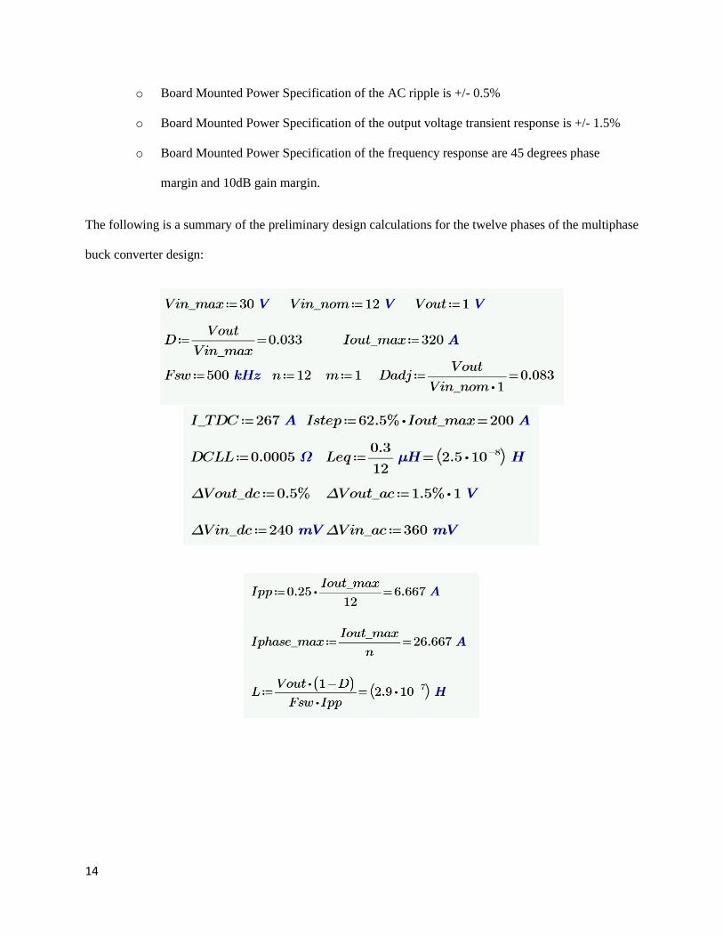
14
o Board Mounted Power Specification of the AC ripple is +/- 0.5%
o Board Mounted Power Specification of the output voltage transient response is +/- 1.5%
o Board Mounted Power Specification of the frequency response are 45 degrees phase
margin and 10dB gain margin.
The following is a summary of the preliminary design calculations for the twelve phases of the multiphase
buck converter design:

15
When additional phases are added to a multiphase buck converter design, the RMS input current
is decreased which in turn decreases the input voltage ripple. The input capacitors, often multi-layer
ceramic capacitors (MLCCs) and aluminum or polymer electrolytic bulk capacitors, are sized
appropriately to handle the input RMS current and provide charge and keep the input voltage within
specifications during load transients.
To keep the output voltage within the tight specifications, a capacitor network mix is needed, and
in practice this would mean a mix of MLCCs. The ceramic capacitors keep the output impedance low
before the control loop can respond during fast transients, minimizing the overshoot and undershoot [9].
Summing the calculated capacitance needed to control the undershoot, the capacitance needed to control
the overshoot, and the capacitance to control the output ripple, a total of approximately 8703uF is
required for the output. The simulated capacitor network shown in Figure 4-3, in addition to each 330uF
capacitor at the output per phase, has a sum of 8718uF.

16
Table 4-1: Bill of Materials (Simulated Entry)
Count RefDes Value Description Size Part Number Manufacturer Per Unit
Cost $
24 U1, U2, U4,
U6, U7, U9, U10, U12,
U13, U15,
U16, U18, U19, U21,
U22, U24,
U25, U27,
U28, U30,
U31, U33,
U34, U36
- 30V -
Enhancement Mode Power
Transistor
6.05mm x
2.3mm
EPC2023 EPC $7.59
12 U3, U5, U8, U11, U14,
U17, U20,
U23, U26, U29, U32,
U35
- 100V - Enhancement
Mode Power
Transistor
3.5mm x
1.95mm
EPC2218 EPC $4.52
12 C2, C3, C5,
C7, C9,
C11, C13, C15, C17,
C19, C21,
C23
220uF CAP CER
220UF 6.3V
X5R
1210 CL32A227MQVNNNE Samsung
Electro-
Mechanics
$1.525
12 C1, C4, C6, C8, C10,
C12, C14,
C16, C18, C20, C22,
C24
330uF CAP CER 330UF 4V
X5R
1210 AMK325ABJ337MM-
T
Taiyo Yuden
$2.415
7 C25 – C31 470uF CAP CER
470UF 2.5V
1812 PMK432C6477MM-T Taiyo Yuden $7.35
20 C32 – C51 47uF CAP CER
47UF 6.3V
0805 CL21A476MQYNNNG Samsung
Electro-
Mechanics
$0.216
25 C52 – C76 22uF CAP CER
0.22UF 10V
X7R
0402 0402B224K100CT Walsin
Technology
Corporation
$0.053
12 D1 – D12 - Schottky 30V
3A
SOD-128 RB050LAM-30 Rohm $0.534
12 L1 – L12 300nH Fixed Inductors
300nH Shld
20% 33.4A
1.17mOhms
8mm x 7.7mm x
7mm
XAL7070301MEC Coilcraft $2.68
Total $379.34

17
Figure 4-1: Phase One of 12-phase Buck Converter Schematic

18
Figure 4-2: Phase Two of 12-phase Buck Converter Schematic (repeated 10 more times)
Figure 4-3: Output Capacitor Mix Network

19
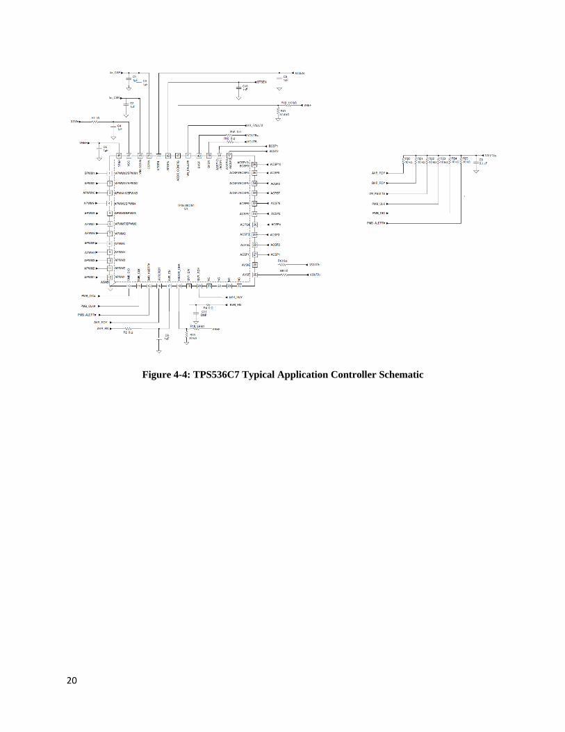
It is also worth noting that the schematic used for simulation purposes is not the final schematic
used in practice for this application. Because of the immaturity of GaN transistors, many workarounds
took place to be able to use the TPS536C7 controller with 12-phase compatibility. The TPS536C7 has
twelve current sensing pins labeled ACSP1 through ACSP12, seen in the controller’s typical application
in Figure 4-4. These pins are optimized for Texas Instrument’s “Smart Power Stages” which are packages
with integrated power stages – integrated MOSFETs and gate drivers. Each current sensing pin expects a
5mV/A signal from the output of each power stage. Being that this design is not optimized for this
controller, this 5mV/A signal must be generated to be able to use this device. This was done by the
construction of a current sense amplifier circuit utilizing the LMP2021 and TLV9062 shown in Figure 4-
5. This setup must be implemented in each individual phase in the design. In this circuit, a shunt resistor
is placed in the path of each output of each individual phase for the purpose of measuring the voltage
across it. The voltage drop of this resistor is then measured by the LMP2021. The output of the LMP2021
is then buffered by the TLV9062, whose output is the input to each current sensing pin of the controller,
providing the 5mV/A signal referenced. Figure 4-6 displays the finished OrCAD PCB layout, and the
finished fabricated board top and bottom sides are shown in Figure 4-7 and 4-8 respectively.
20
Figure 4-4: TPS536C7 Typical Application Controller Schematic

21
Figure 4-5: Current Sensing Circuitry for TPS536C7

22
Figure 4-6: OrCAD PCB Editor Board Layout
Figure 4-7: Fabricated Board (Top)

23
Figure 4-8: Fabricated Board (Bottom)
Chapter 5: Simulation Results and Analysis
OrCAD Simulation Setup
This GaN multiphase buck converter was simulated in OrCAD PSpice 17.4. The schematic
excludes the TPS536C7 controller and UP1966D GaN FET driver but uses pulsed voltage sources to
simulate the PWM signal that would be sent to each individual phase. The first page of the schematic is
the first phase of the buck converter, shown in Figure 5-1, also shows some of the design parameters
including the duty cycle, switching period, and the timing delays that are required for each subsequent
phase.
The voltage source input for the buck converter is 12V. Models for the high-side GaN FET
(EPC2218), low-side GaN FET (EPC2023), and the Schottky diode (DRB050LAM-30), used to help
accommodate for the EPC2023’s slow reverse recovery, have been imported into the simulation. The

24
runtime is set for 5ms to display the reaching of steady-state. The performance of this multiphase buck
converter is extracted from the overall performance of each inductor current, output voltage, total current
supplied, and steady-state efficiency. For the output voltage to be close to the desired 1V, the duty cycle
had to be decreased from the theoretical 0.083 to 0.0795. In simulation, this duty cycle yields an average
output voltage of 1.002V at steady-state.
Figure 5-1: First Phase of Multiphase Buck Converter with Parameters
Buck Converter Timing and Driving Dead-Time
The switching period in this simulation is 2us, yielding a switching frequency of 500kHz. The
simulation was also run at 1MHz and 2MHz as well. All pulsed voltage sources in this design must have a
slight offset between each phase so that no two phases are firing at once. This includes both high and low-

25
side gate driving. The amount in degrees to separate each phase by is calculated by dividing 360° by the
number of phases present. Hence, the appropriate spacing for this design is 30°. Translating this phase
shift into time, with a switching period of 2us, equates to approximately 167ns. This phase shift can be
seen in Figure 5-2 across all twelve phases.
Figure 5-2: High-Side Gate Voltage Source Pulsing with 30° Phase Shift
For this application, the duty cycle is calculated to be 0.083. This value of the duty cycle
translates into the high-side switching device (EPC2218) being on 8.33% of the switching period, the
other 91.67% is the low-side switching device (EPC2023) being on. These two switching devices cannot
be on at the same time. When either FET is on at the same time, this will cause current spiking in the
inductor and possibly destroy or burn out the inductor, among other components present as well. To avoid
this, dead-time between the driving of the high-side and low-side is introduced, “cushioning” the area in
which otherwise both FETs would be on at the same time. In this simulation, 30ns of dead-time was used,
shown in Figure 5-3.

26
Figure 5-3: High-Side FET (Green) and Low-Side FET (Red) Gate Driving
Inductor Current
The twelve different inductor current waveforms are shown in Figure 5-4. The phases are all,
nearly, equally sharing the targeted maximum current draw of 320A and are out of phase with each other
by 30°. The average of each inductor current, at steady-state, ranges between 24.53A and 28.85A. Figure
5-5 displays the total inductor current of 322.87A, this current is the sum of all 12 individual inductor
currents.

27
Figure 5-4: Individual Inductor Current
Figure 5-5: Average Inductor Current (Output Current)
Output Voltage
Figures 5-6 and 5-7 show the average output voltage waveform and its corresponding ripple. The
average steady-state output voltage is 1.002V with a voltage ripple of 0.05mV.

28
Figure 5-6: Average Output Voltage
Figure 5-7: Output Voltage Ripple

29
Power and Efficiency
In Figure 5-8, the input and output waveforms are shown. The input power is measured to be
357.61W and the output power is measured to be 341.46W at steady-state. Calculating the overall
efficiency of the multiphase buck converter, with a switching frequency of 500kHz at full load, it is
calculated to be 95.46%. The efficiency at 1MHz and 2MHz are 93.13% and 90.15%, respectively.
Figure 5-8: Input (Green) and Output (Red) Power

30
Summary
Table 5-1 summarizes the simulation results gathered.
Table 5-1: Simulation Result Summary
Parameter Simulation Result
Output Voltage 1.002V
Output Voltage Ripple @ 320A 3.29mV
Efficiency at steady-state (500kHz) 95.46%
Efficiency at steady-state (1MHz) 93.41%
Efficiency at steady-state (2MHz) 89.90%
Data Analysis
After simulation and the inspection of various waveforms of interest, the design is operating
mostly as expected. There are some slight variations present in the individual inductor current waveforms.
The inductor in the first phase seems to have more current traveling through it than the other eleven
phases at 28.85A. This could be due to the slight imbalance in the timing of the gate-driving sources.
Another area of concern is the decrease in duty cycle to obtain the output voltage. Often in
simulation, one would have to overcompensate in different areas to obtain the desired outcome. Here, the
duty had to be decreased to 0.0795 to achieve an average output voltage within specifications. With a
fixed input voltage source, the only area that would affect the duty cycle is the voltage at the output. With
a constant 320A DC current draw at the output, there must be some other type of voltage imbalance
taking place at the output that is causing this issue.
The output voltage waveform does have a reasonably sized overshoot that was expected to be
mitigated by the output capacitor mix network. It is possible that the reason why this area was not taken

31
care of was because ideal capacitors were used in the simulation, and not models for real-world capacitors
for various MLCCs, aluminum or polymer electrolytic bulk capacitors.
Chapter 6: Conclusion
This project explored the design and simulation of a multiphase buck converter, implementing
GaN MOSFETs as the high and low-side switching devices. The goal of this project was to investigate
how GaN devices perform in low-voltage, multiphase buck converter applications for a high current
requirement. This multiphase buck converter receives a 12V input and, in simulation, successfully outputs
the required maximum of 320A at 1V in an efficient manner.
The DC and AC output voltage design constraints were met, as well as the increase in efficiency
by at least 2% from Cisco System’s JMAC, but of course this is only the results of the simulation and the
board must be tested in the lab to investigate further. A future design change that can be implemented in
the simulated work is importing real capacitor models for all capacitors present. This implementation may
help the overshoot of the output voltage and dampen the waveform to fall within Cisco’s BMP
requirements. In real-world application, this issue can easily be mitigated through live troubleshooting of
the multiphase buck converter.
Due to the immaturity of GaN MOSFETs, the phase segment not exceeding 0.3451in^2
specification could not be met. It is also expected, that during future testing of the board, an increase in
current density of 30% and thermal shift reduction in RDS-on of 10% specifications will also not be
satisfied as well. These specifications could not be met because as of present, there are no public
integrated Driver-GaN devices that would reduce the size of the power stage and also simultaneously
meet the high current requirement of this design.
Although the design meets the output power and an increase in efficiency specification, there are
a remainder of specifications that cannot yet be explored due to the inability to test this board in person at

32
present. In future work, the board will be assembled and tested at Cisco System’s lab facilities. The
multiphase buck converter will be fully characterized for the Board Mounted Power Supply team, and
they will determine next steps for this project and its design.

33
References
[1]. Taufik, Introduction to Power Electronics, Lulu Publishing, September 2020, ISBN
9781716695865.
[2]. “Isolated vs Non-Isolated Power Converters,” CUI Inc, 03-Dec-2019. [Online]. Available:
https://www.cui.com/blog/isolated-vs-non-isolated-power-converters. [Accessed: 11-Jan-
2021].
[3]. “Buck Converter: Basics, Working, Design and Operation,” Components101, 26-Apr-2019.
[Online]. Available: https://components101.com/articles/buck-converter-basics-working-
design-and-operation. [Accessed: 11-Jan-2021].
[4]. “Multiphase Buck Design From Start to Finish (Part 1),” ti.com, Apr-2017. [Online].
Available:
https://www.ti.com/lit/an/slva882a/slva882a.pdf?ts=1603824277756&ref_url=https%253A
%252F%252Fwww.google.com%252F. [Accessed: 11-Jan-2021].
[5]. Cao, P.; Ng, J.C.W.; Trescases, O., "Thermal management for multiphase current mode buck
converters," Applied Power Electronics Conference and Exposition (APEC), 2011 Twenty-
Sixth Annual IEEE , vol., no., pp.1124,1129, 6-11 March 2011
[6]. S. Pattnaik, A. K. Panda and K. K. Mahapatra, "An Improved Multiphase converter for New
Generation Microprocessr," 2008 IEEE Region 10 and the Third international Conference on
Industrial and Information Systems, Kharagpur, 2008, pp. 1-5, doi:
10.1109/ICIINFS.2008.4798427.
[7]. B. K. Rhea et al., "A 12 to 1 V five phase interleaving GaN POL converter for high current low
voltage applications," 2014 IEEE Workshop on Wide Bandgap Power Devices and
Applications, Knoxville, TN, 2014, pp. 155-158, doi: 10.1109/WiPDA.2014.6964645.
[8]. U. Ahmad, S. Wu, “Analysis of Improved Multiphase Buck Converter,” California Polytechnic
State University, San Luis Obispo, June 2018
[9]. C. Parisi, “Multiphase Buck Design from Start to Finish (Part 1)”, Texas Instruments, April
2017 – Revised May 2019
[10]. Cisco internal resource.
[11]. Efficient Power Conversion, “EPC2023 – Enhancement Mode Power Transistor”, Efficient
Power Conversion, 2020
[12]. Efficient Power Conversion, “Fast Just Got Faster Blog – Technical Characteristics of GaN
and SiC”, Efficient Power Conversion, 2020
[13]. J. Browne, “GaN Material Costs Dropping Over Time”, Microwaves & RF , March 2013

34
[14]. L. Hoffmann, C. Gautier, S. Lefebvre, and F. Costa, " Optimization of the Driver of GaN
Power Transistors Through Measurement of Their Thermal Behavior," IEEE Trans. Power
Elec, August 2013.
[15]. Efficient Power Conversion, “EPC 2023 – Enhancement Mode Power Transistor”, Datasheet,
Efficient Power Conversion, Revised June 2020
[16]. A. Bindra, “Selecting Gate Driver ICs fir Gallium Nitride FETs”, Electronic Products, January
2013

35
Appendices
A. Final Schematic
Figure A-1: First Phase of Design, including design parameters

36
Figure A-2: Second Phase of Design
Figure A-3: Third Phase of Design

37
Figure A-4: Fourth Phase of Design
Figure A-5: Fifth Phase of Design

38
Figure A-6: Sixth Phase of Design
Figure A-7: Seventh Phase of Design

39
Figure A-8: Eighth Phase of Design
Figure A-9: Ninth Phase of Design

40
Figure A-10: Tenth Phase of Design
Figure A-11: Eleventh Phase of Design

41
Figure A-12: Twelfth Phase of Design
B. Project Schedule

42
C. Bill of Materials (Actual)
Count Value Description Size Part Number Manufacturer Per Unit
Cost $
24 - 30V -
Enhancement Mode Power
Transistor
6.05mm x
2.3mm
EPC2023 EPC Donated
12 - 100V -
Enhancement Mode Power
Transistor
3.5mm x
1.95mm
EPC2218 EPC Donated
20 0.1UF CAP CER
0.1UF 16V
X7R 0402
0402 0402YC104JAT4A AVX Corporation $0.05
20 0.22UF CAP CER 0.22UF 10V
X7R 0402
0402 0402B224K100CT Walsin Technology
Corporation
$0.05
20 1UF CAP CER 1UF
16V X7R 0603
0603 0603YC105JAT2A AVX Corporation $0.19
10 1000PF CAP CER
1000PF 50V
X7R 0402
0402 CL05B102JB5NNNC Samsung Electro-
Mechanics
$0.04
10 1UF CAP CER 1UF
6.3V X7R 0402
0402 CL05B105KQ5NQNC Samsung Electro-
Mechanics
$0.12
50 220UF CAP CER
220UF 6.3V
X5R 1210
1210 CL32A227MQVNNNE Samsung Electro-
Mechanics
$1.33
65 22UF CAP CER
22UF 25V X5R
1206
1206 CL31A226KAHNNNE Samsung Electro-
Mechanics
$0.19
20 4.7UF CAP CER
4.7UF 25V
X5R 0805
0805 CL21A475KAQNNNE Samsung Electro-
Mechanics
$0.08
27 560UF CAP ALUM
POLY 560UF
20% 2V SMD
7343 EEF-GX0D561L Panasonic Electronic
Components
$1.68
10 220UF CAP TANT POLY 220UF
16V 2917
2917 TCJD227M016R0050E AVX Corporation $1.54
15 0.001
OHM
RES 0.001
OHM 1% 2W
2512
2512 WSL25121L000FEA18 Vishay Dale $1.86

43
60 0 OHM RES 0 OHM JUMPER
1/16W 0402
0402 CRCW04020000Z0EDC Vishay Dale $0.02
10 1 OHM RES SMD 1
OHM 1%
1/16W 0402
0402 RC0402FR-071RL Yageo $0.03
10 10K OHM RES SMD 10K OHM 0.1%
1/16W 0402
0402 ERA-2AEB103X Panasonic Electronic
Components
$0.28
10 20K OHM RES SMD 20K
OHM 0.1%
1/16W 0402
0402 ERA-2AEB203X Panasonic Electronic
Components
$0.28
30 1K OHM RES SMD 1K
OHM 0.1%
1/16W 0402
0402 ERA-2AEB102X Panasonic Electronic
Components
$0.28
30 30K OHM RES SMD 30K
OHM 0.1%
1/16W 0402
0402 ERA-2AEB303X Panasonic Electronic
Components
$0.28
10 38.3K
OHM
RES SMD
38.3K OHM
0.1% 1/16W
0402
0402 RT0402BRD0738K3L Yageo $0.32
30 5.1K OHM RES SMD 5.1K
OHM 0.1%
1/16W 0402
0402 RT0402BRD075K1L Yageo $0.32
10 59K OHM RES SMD 59K
OHM 0.1%
1/16W 0402
0402 RT0402BRD0759KL Yageo $0.32
20 - RB050LAM-30
SCHOTTKY
BARRIER
- RB050LAM-30TR Rohm
Semiconductor
$0.53
30 - TERM SCREW 10-32 6 PIN
PCB
- 8196 Keystone
Electronics
$0.84
1 - CONN HEADER SMD
3POS 2.54MM
- TSM-103-01-T-SV-P-TR Samtec Inc. $0.94
20 1UF CAP CER 1UF
6.3V X5R 0402 0402 CGB2A3X5R0J105M033BB TDK Corporation $0.11
15 - IC CMOS 1
CIRCUIT
SOT23-5
SOT23-5 TLV9061IDBVR Texas Instruments $0.58
15 - IC OPAMP GP 2 CIRCUIT
8VSSOP
8VSSOP LMV862MM/NOPB Texas Instruments $2.54

44
12 3.3uH Fixed Inductors Fixed Inductors
3.3uH Shld
20% 15.1A 9.42mOhms
AECQ2
AECQ2 XAL7070-332MEB Coilcraft $3.14
12 - Dual Channel
Synchronous
Gate Driver for
Enhancement
Mode GaN
Transistors
- UP1966D UPI Donated
1 - Board
Fabrication
- - Avanti Circuits $1,125.00
Total $1465.04
D. Analysis of Senior Project Design
Project Title: Multiphase Buck Converter Implementing Gallium Nitride Semiconductors
Student: Kadin Stephens
Advisor: Dr. Taufik
1. Summary of Functional Requirements
The requirements of this senior project revolve around the existing capabilities of the original
Cisco JMAC point-of-load converter. At a minimum, this new point-of-load converter must accommodate
a total current of 320A, at 1V, at the output. The board receives a 12V-in supply voltage and steps it down
to the 1V output. GaN devices are known for their efficiency, using them in this design allows for an
increase in efficiency of at least 2% from the original design. Also, GaN devices can reduce the form
factor of a design. Using this to one’s advantage, an increase of 30% in current density, a thermal shift
reduction in RDS-on of 10%, and a size of 0.3451in2 for a single-phase segment is the goal. This new
design will utilize 12 phases.

45
2. Primary Constraints
Significant challenges with this design project include the lack of GaN devices on the public
market because the technology is newer, putting together selection criteria of said devices, and gate-driver
and controller selection is difficult. Because GaN technology is newer there are not a lot of devices
available on the market as compared to traditional silicon devices (MOSFETs). Efficient Power
Conversion (EPC) has made great strides in expanding this technology more and has a wide variety of
high to low voltage GaN devices. The selection criteria of these GaN FETs was something I have not
considered before for other projects I have had in school. Since one of the specifications for this project is
an increase in efficiency, one must be concerned about the drain-to-source voltage rating of the GaN FET
that is chosen. The farther and farther away from 12V-in you are, the more the efficiency will decrease
since higher voltage FETs are not manufactured for low-voltage applications. Also, since there are no
Driver-GaN (DrGaN) devices (integrated circuits with an internal driver and the GaN FET) on the market,
this makes things more complicated when selecting outside components to drive your hardware.
Another constraint that was unanticipated was the design compatibility with the TPS536C7
controller. The TPS536C7 is a step-down, multiphase PWM controller that is capable of driving up to
twelve gate-drives and also monitor the output of the multiphase buck converter to adjust it’s output
voltage. The controller has current sensing pins that are optimized for Texas Instrument’s “Smart Power
Stages” and expect a 5mV/A signal. Because this design is not optimized for this controller, the 5mV/A
signal needs to be generated on board so the controller can properly take output voltage measurements
and provide feedback. This signal was generated by constructing a current sense amplifier circuit using
TI’s TLV9062 and LMP2021 operational amplifiers.
3. Economic
(a) Human Capital: One of the requirements of this project is a detailed test report covering
functional parameters of the generated demonstration board. This requirement motivates myself to drive

46
towards the presentation of my findings to my colleagues and advisor. Leading up to reporting the
findings of this work, I would have strengthened my electrical engineering skills, and exercised testing
methods that I have learned during my time in university. My advisor and Cisco colleagues will capitalize
from this project because they would learn more about GaN devices and their characterization, possibly
leading to the inspiration to implement the technology on their own.
(b) Financial Capital: If this research turns into something that Cisco would use on their own
products, the monetary value would be defined by them. Included in this financial capital as well are my
wages throughout the course of the project, procurement of components and materials for the project,
fabrication of the test board, and traveling to and from Cisco Systems’ facilities to perform testing and
analysis.
(c) Natural Capital: The Gallium Nitride FETs used in this project have semiconductor
material(s) that are used to produce the desired effect. Gallium Nitride is a synthetic compound, being
that it is man-made, but there are natural gases that are used in the crystallization processes. These natural
gases are collected from the Earth. The methodologies used to collect natural gasses have the potential to
poison groundwater, pollute surface water, and damage wildlife.
• Costs start to accrue during the procurement of the components that are used. The GaN devices, gate-
drivers, and controllers are not inexpensive compared to other devices on the market. Benefits start to
show up once the system is built, or at least simulated, and one can witness the potential efficiency
earnings.
• The project requires an input of 12V, ideally coming from a source that has little to no noise associated
with it, as close to pure DC as possible. The project costs approximately $1500. These costs will be paid
out of the budget of Cisco’s Board Mounted Power team.
• The original cost of this project was anticipated to be less than $150, excluding the board fabrication.
This did not take into consideration having to purchase the gate-driver(s) separately from the GaN devices
and additional components needed to make the design compatible with the controller.

47
• The equipment that is needed for development include: a soldering iron/gun, lead free solder, a
desoldering pump, a fume extraction fan, and safety glasses.
• The earnings are endless, being that Cisco is a successful company that produces a wide product line all
needing some type of power conversion. Implementing GaN technology also increases power savings,
saving money which is also attractive.
• Products would emerge after a potential decision to adapt this technology is made by Cisco.
Maintenance costs would be dependent on the pay scales of those assigned to this project and who will
upkeep its production and innovation.
• The original production time of this project, from start to finish, is 6 months.
• After the project ends and the findings/research are reported back to Cisco’s Board Mounted Power
Team, a decision will be made by the team whether or not this technology should be pursued or if it is not
ready for the redirected resources.
4. If manufactured on a commercial basis:
• The estimated number of devices sold per year would be dependent on the amount of Cisco products
this point-of-load converter is adapted into. I will use a sample number of 1000. This number is
significantly small in comparison to an actual volume amount of how many products Cisco would sell on
a yearly basis, that include this type of power conversion.
• The estimated manufacturing cost for this design ranges from $1300 - $1550. This estimate includes the
component costs as well as the cost of having the design fabricated. This range also includes possible
savings from buying components in bulk. If the design were implemented into a project, just purchasing
the components would be at most $600.
• The estimated purchase price for each board would be $2550, at most. This is the purchase price of the
complete test board, whereas if this design was implemented into an existing project, the purchase price
for implementation would be $900.

48
• The estimated profit per year, of the complete test board, would be $850,000.
• The estimated cost for the user to operate this device is dependent on what device the converter is in.
5. Environmental
• The environmental impact of this project would be dependent on the manufacturing methods used by
EPC to make these GaN devices. A point of development of concern is the manufacturing of
semiconductors. In the manufacturing process of semiconductors, there are byproducts produced that can
affect air, water, and wildlife. Other processes contributing to the same downfalls are PCB manufacturing
and integrated circuit packaging manufacturing.
• This project indirectly uses natural gases. Natural gasses are needed for manufacturing plants as well as
the production of Gallium Nitride.
• This project could potentially contribute to the degradation of the Earth via pollutants created by the
manufacturing plants that make semiconductor devices, PCB boards, and integrated circuit packaging.
The use of these devices can also help the Earth, when used in electric vehicles it can make the vehicle
potentially more power efficient which would reduce the need for having to charge up the vehicle
frequently.
• Various manufacturing processes can harm nearby wildlife directly by killing them during the building
process of manufacturing plants and by the pollutants poisoning their resources of food and water.
6. Manufacturability
The manufacturability of this design includes procurement of the needed devices and fabrication
of the complete test board. Component placement in this project will be completely outsourced, the
fabrication plant will populate all the components on the PCB board through a reflow method. Also, using
standard manufacturing equipment for the fabrication of GaN can produce material stresses and defects in
the GaN devices. Using manufacturing equipment that is specifically made to produce GaN can
potentially mitigate these issues.

49
7. Sustainability
• The main issue of maintaining this device/product, is that it is limited by the amount of natural gases the
Earth contains and the amount of areas people can effectively use fracking technologies in, for production
of GaN devices. Another area of limitation is the materials needed to produce and manufacture capacitors,
inductors, resistors, and PCB material.
• The project impacts the sustainable use of the Earth’s natural gases, and materials used to produce
capacitors, inductors, resistors, among other electronic devices used in this project.
• An upgrade of how Gallium Nitride is produced could help by reducing the amount of natural gas that is
needed in the production process, which would reduce consumption. Exploration in the material use in the
other electronic devices that fill this design can be of some benefit as well, always looking for better
material to utilize.
• The issues that could prevent upgrading the design of GaN devices are loss of interest by companies
pulling out of the venture to expand on this technology. This would cease the innovation of GaN.
8. Ethical
IEEE Code of Ethics II: To improve the understanding by individuals and society of the
capabilities and societal implications of conventional and emerging technologies, including intelligent
systems.
• Satisfied by providing project technical reports about this emerging technology.
IEEE Code of Ethics IV: To avoid unlawful conduct in professional activities, and to reject
bribery in all its forms.
• Exposed to constant vendor communication, those who may or may not try different
ways to win business.

50
IEEE Code of Ethics V: To seek, accept, and offer honest criticism of technical work, to
acknowledge and correct errors, to be honest and realistic in stating claims or estimates based on available
data, and to credit properly the contributions of others.
• Continued design review check-ins to receive and explain project information. Working
in solutions that best fit the overall success of the project.
9. Health and Safety
Direct health concerns would stem from the fracking method used to collect the natural gas that is
needed to produce Gallium Nitride. The pollution of the air could have great health effects on the public.
Also, because the project’s output current has a maximum capability of 320A, there is a shock hazard that
is associated with operating the device externally, when it is not enclosed. The high wattage present in the
design when it is performing at full load does present a potential fire hazard if a fault or short were to
occur. The controller used in the design does have over-current protection that would cease the driving of
the PWM signal to the power stage(s) which would diminish the output. Once housed in another product,
this potential issue would become of minimal concern.
10. Social and Political
• Since this project involves continued use of natural gas collection, there are national and worldwide
concerns for the continued efforts of depleting the Earth’s natural resources. This affects every single
person on the planet and will affect future generations as well. If laws are not passed to limit the depletion
of these resources or to allocate money and resources to the research of improving our current methods,
we will destroy our planet eventually.
• This project can potentially impact any country that has adapted widely the use of electric vehicles.
Electric vehicles are positively contributing to the preservation of Earth, and GaN has the potential to
become more implemented in electric vehicles to improve power efficiency.
• This project would benefit stakeholders, in that if this technology is adapted it will push our electronic

51
devices in the direction of improved power efficiencies, which saves money. On the other end, it would
negatively impact stakeholders of companies that produce traditional silicon semiconductors. This
adaption would ultimately create more jobs than it would take away. The reason being is because the wide
adaption would create opportunities to replace all inefficient, when compared to utilizing GaN,
semiconductors that are in our everyday devices.
• The project would create inequities caused by the displacement of traditional silicon semiconductors.
• The wide adaption of this technology in our everyday devices could have a ripple effect, affecting
decision making in governments for topics such as electronic devices, electric vehicle regulation, how
power is distributed, etc.…
11. Development
There were two new tools that I utilized for this project for the development and analysis of this
design. The first tool is EPC’s “GaN FET Selection Tool for Buck Converters”. In this tool, I was able to
place in my various design specifications such as input voltage, output voltage, frequency, and deadtime
requirement to generate a report of what GaN FET(s) in EPC’s library would best fit my requirements.
Using this tool, and communicating with an EPC applications engineer, I was able to come to the
educated choice of selecting the EPC2023 and EPC2218 as my switching devices in this multiphase buck
converter application.
The second tool that I was somewhat familiar with but ended up using a lot for this project is
OrCAD. During my stay at Cal Poly, I mostly used Analog Devices’ “LTspice XVII” for my schematic
entry and simulation purposes. For this project, I decided that using OrCAD’s “Capture CIS” and “PSpice
AD” would be the most beneficial to me because it seemed that it was more straight forward to import
models for different components I wanted to use that were not already in OrCAD’s library.

52
Special Thanks
Jessica Kiefer, Kami H., Mimi T., and Cisco Systems’ Board Mounted Power Team
Stu C., Cassidy A., Jayanth K., and Raymundo H. from Texas Instruments
Mark G. from Efficient Power Conversion
Ron V. from uPI Semiconductor