Free-Standing Self-Assemblies of Gallium Nitride ...
22
micromachines Review Free-Standing Self-Assemblies of Gallium Nitride Nanoparticles: A Review Yucheng Lan 1, *, Jianye Li 2 , Winnie Wong-Ng 3 , Rola M. Derbeshi 1 , Jiang Li 4 and Abdellah Lisfi 1 1 Department of Physics and Engineering Physics, Morgan State University, Baltimore, MD 21251, USA; [email protected] (R.M.D.); Abdellah.Lisfi@morgan.edu (A.L.) 2 Department of Materials Science and Engineering, University of Wisconsin-Madison, Madison, WI 53706, USA; [email protected] 3 Materials Science Measurement Division, National Institute of Standards and Technology, Gaithersburg, MD 20899, USA; [email protected] 4 Department of Civil Engineering, Morgan State University, Baltimore, MD 21251, USA; [email protected] * Correspondence: [email protected]; Tel.: +1-443-885-3752 Academic Editor: Massimo Mastrangeli Received: 6 April 2016; Accepted: 12 July 2016; Published: 19 July 2016 Abstract: Gallium nitride (GaN) is an III-V semiconductor with a direct band-gap of 3.4 eV. GaN has important potentials in white light-emitting diodes, blue lasers, and field effect transistors because of its super thermal stability and excellent optical properties, playing main roles in future lighting to reduce energy cost and sensors to resist radiations. GaN nanomaterials inherit bulk properties of the compound while possess novel photoelectric properties of nanomaterials. The review focuses on self-assemblies of GaN nanoparticles without templates, growth mechanisms of self-assemblies, and potential applications of the assembled nanostructures on renewable energy. Keywords: self-assembly; nanoparticles; GaN nitride; renewable energy; review 1. Introduction Gallium nitride (GaN) based semiconductors have attracted great attentions since the 1990s [1–4]. GaN is a binary III–V direct band-gap semiconductor. Wurtize GaN has a space group of P6 3 mc with lattice constants a = 3.1891(1) Å and c = 5.1853(3) Å [5]. Its wide band gap of 3.4 eV [6,7] affords the nitride special properties for applications in optoelectronic, high-power and high-frequency devices, high-temperature microelectronic devices, and bright lighting sources. For example, (1) hexagonal GaN crystalline films have been fabricated as blue light emitting diodes (LEDs) [3,4,8–10] because of its special optical emission [11,12]. The alloyed InGaN- and AlGaN-based LEDs can emit colorful light from red to ultra-violet [9]; (2) GaN films have been employed to make violet (about 405 nm) laser diodes (LDs) [3,4], without use of nonlinear optical frequency-doubling; (3) The first GaN-based metal-semiconductor field-effect transistors (MESFET) were experimentally demonstrated in 1993 [13] and commercially available in 2010. High-speed field-effect transistors and high-temperature microelectronic devices were also developed using the material [2] in the 1990s; (4) GaN high-electron-mobility transistors (HEMTs) have been commercialized since 2006, applied at high efficiency and high voltage operation. GaN transistors can operate at much higher temperatures and work at much higher voltages than gallium arsenide transistors. GaN HEMTs are ideal power amplifiers at microwave frequencies; (5) GaN materials have also been utilized as renewable energy materials, such as in thermoelectric devices [14–17] to harvest waste heat, betavoltaic microbatteries [18–20] to collect energy from radioactive sources emitting beta particles, and solar cells [21] to collect solar energy. More applications of GaN materials can be found in some review literatures [1,2,4,22]. Micromachines 2016, 7, 121; doi:10.3390/mi7070121 www.mdpi.com/journal/micromachines
Transcript of Free-Standing Self-Assemblies of Gallium Nitride ...

micromachines
Review
Free-Standing Self-Assemblies of Gallium NitrideNanoparticles: A Review
Yucheng Lan 1,*, Jianye Li 2, Winnie Wong-Ng 3, Rola M. Derbeshi 1, Jiang Li 4 and Abdellah Lisfi 1
1 Department of Physics and Engineering Physics, Morgan State University, Baltimore, MD 21251, USA;[email protected] (R.M.D.); [email protected] (A.L.)
2 Department of Materials Science and Engineering, University of Wisconsin-Madison, Madison, WI 53706,USA; [email protected]
3 Materials Science Measurement Division, National Institute of Standards and Technology, Gaithersburg,MD 20899, USA; [email protected]
4 Department of Civil Engineering, Morgan State University, Baltimore, MD 21251, USA; [email protected]* Correspondence: [email protected]; Tel.: +1-443-885-3752
Academic Editor: Massimo MastrangeliReceived: 6 April 2016; Accepted: 12 July 2016; Published: 19 July 2016
Abstract: Gallium nitride (GaN) is an III-V semiconductor with a direct band-gap of 3.4 eV. GaN hasimportant potentials in white light-emitting diodes, blue lasers, and field effect transistors because ofits super thermal stability and excellent optical properties, playing main roles in future lighting toreduce energy cost and sensors to resist radiations. GaN nanomaterials inherit bulk properties ofthe compound while possess novel photoelectric properties of nanomaterials. The review focuses onself-assemblies of GaN nanoparticles without templates, growth mechanisms of self-assemblies, andpotential applications of the assembled nanostructures on renewable energy.
Keywords: self-assembly; nanoparticles; GaN nitride; renewable energy; review
1. Introduction
Gallium nitride (GaN) based semiconductors have attracted great attentions since the 1990s [1–4].GaN is a binary III–V direct band-gap semiconductor. Wurtize GaN has a space group of P63mc withlattice constants a = 3.1891(1) Å and c = 5.1853(3) Å [5]. Its wide band gap of 3.4 eV [6,7] affordsthe nitride special properties for applications in optoelectronic, high-power and high-frequencydevices, high-temperature microelectronic devices, and bright lighting sources. For example,(1) hexagonal GaN crystalline films have been fabricated as blue light emitting diodes (LEDs) [3,4,8–10]because of its special optical emission [11,12]. The alloyed InGaN- and AlGaN-based LEDs canemit colorful light from red to ultra-violet [9]; (2) GaN films have been employed to make violet(about 405 nm) laser diodes (LDs) [3,4], without use of nonlinear optical frequency-doubling;(3) The first GaN-based metal-semiconductor field-effect transistors (MESFET) were experimentallydemonstrated in 1993 [13] and commercially available in 2010. High-speed field-effect transistorsand high-temperature microelectronic devices were also developed using the material [2] in the1990s; (4) GaN high-electron-mobility transistors (HEMTs) have been commercialized since 2006,applied at high efficiency and high voltage operation. GaN transistors can operate at much highertemperatures and work at much higher voltages than gallium arsenide transistors. GaN HEMTsare ideal power amplifiers at microwave frequencies; (5) GaN materials have also been utilized asrenewable energy materials, such as in thermoelectric devices [14–17] to harvest waste heat, betavoltaicmicrobatteries [18–20] to collect energy from radioactive sources emitting beta particles, and solarcells [21] to collect solar energy. More applications of GaN materials can be found in some reviewliteratures [1,2,4,22].
Micromachines 2016, 7, 121; doi:10.3390/mi7070121 www.mdpi.com/journal/micromachines
Micromachines 2016, 7, 121 2 of 22
GaN is not sensitive to ionizing radiation, making it a suitable material working in radiationenvironments. Therefore, the GaN-based devices, including LEDs, LDs, MESFETs, HEMTs, andsolar cells, have valuable applications in military and out space activities, showing stability inradiation environments.
To date, GaN nanoparticles [23], nanorods [24–31], nanowires [32–41], and nanotubes [24,42–47]have been synthesized using a variety of techniques besides single crystals [48–52]. Compared withGaN crystalline bulks and films, GaN nanomaterials usually show tuning optical properties [53] andmore interesting behaviors because of the quantum confinement, having wider applications [54] thanbulks and films. Individual crystalline nanorods and nanowires have been utilized as nano-LEDs [55],LDs [56–58], and field effect transistors [59,60]. Assemblies of nanorods and nanowires have also beenfabricated into nanowire LEDs [61–63], nanorod LEDs [64], and nano generators [65,66].
GaN nanoparticles have the highest surface / volume ratio among all GaN nanomaterials. Herewe focus on free-standing self-assemblies of GaN nanoparticles. Syntheses and physical properties ofGaN nanoparticles will be introduced, followed free-standing self-assemblies of GaN nanoparticles.The unique physical properties and potential applications of the free-standing assemblies are discussedat the end.
2. Syntheses of GaN Nanoparticles
Hexagonal GaN nanoparticles have been synthesized by various techniques. Among thesetechniques, chemical vapor deposition, nitridation, solvothermal technique, and ball-milling arepopular methods to produce GaN nanoparticles. Table 1 compares these four kinds of methods.
Table 1. Typical syntheses of gallium nitride (GaN) nanoparticles.
Method Precursors Catalysts Reaction Temperature (◦C) Average Diameter (nm) Reference
CVD Ga - 900–1150 5–8 [67]nitridation Ga2O3 - 800–1100 40–500 [68]
GaSb - 900 14–23 [69]Ga(NO3)3 - 850 5 [70]GaO(OH) - 900–1000 12–15 [71]
solvothermal Ga † Li 350–500 30–70 [23]Ga † NH4I 350–500 12 [72]GaCl3 ‡ Li3N 280 30 [73]
ball milling Ga and NH3 - 100 10–30 [74]†: ammono-thermal; ‡: benzene-thermal.
2.1. Chemical Vapor Deposition
GaN nanoparticles can be easily prepared from a reaction of gallium and ammonia by chemicalvapor deposition (CVD) methods at 900–1150 ◦C [5,49,67,68,75], and from organic gallium compoundsby detonations or pyrolysis [76–78].
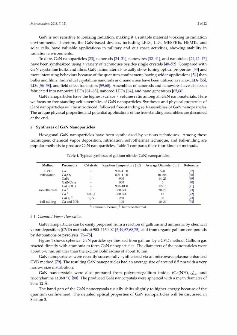
Figure 1 shows spherical GaN particles synthesized from gallium by a CVD method. Gallium gasreacted directly with ammonia to form GaN nanoparticles. The diameters of the nanopaticles wereabout 5–8 nm, smaller than the exciton Bohr radius of about 10 nm.
GaN nanoparticles were recently successfully synthesized via an microwave plasma-enhancedCVD method [79]. The resulting GaN nanoparticles had an average size of around 8.5 nm with a verynarrow size distribution.
GaN nanocrystals were also prepared from polymericgallium imide, (Ga(NH)3/2)n, andtrioctylamine at 360 ◦C [80]. The produced GaN nanocrystals were spherical with a mean diameter of30± 12 Å.
The band gap of the GaN nanocrystals usually shifts slightly to higher energy because of thequantum confinement. The detailed optical properties of GaN nanoparticles will be discussed inSection 3.
Micromachines 2016, 7, 121 3 of 22
The CVD synthesized GaN nanoparticles usually crystallized well because of higher reactiontemperature. However, there are nitrogen- or gallium-vacancies in CVD-grown GaN nanoparticles,affecting optical properties. The details will be discussed in Section 3.
It is challenging to produce massive GaN nanoparticles using the CVD methods because of highcost of starting materials and low product yields.
230
2 Results and discussion
A scanning electron microscopic image (Fig. 1a) shows thata layer of separated particles, which are distributed randomly,are deposited on the substrate surface. The particles havediameters of between 30 and 50 nm. We find that each par-ticle is composed of agglomerated spherical particles thathave diameters of about 5–8 nm (Fig. 1b) under larger mag-nification. The size is smaller than the exciton Bohr radiusof about 10 nm. Electron dispersive analysis (EDS) showsthat the particles contain only Ga and N. The X-ray pow-der diffraction pattern (Fig. 2) shows that the products areGaN with a wurtzite structure. Some diffraction peaks arebroadened due to nano-sized effects. Transmission electronmicroscopy (TEM) observation revealed that no GaN wettinglayer could be observed. The agglomerated dots seem to growdirectly on the LaAlO3 substrate surface. The combination ofthe NH3 flow rate, growth temperature, and growth time arefound to be key factors in determining the dot size and thedensity of particles.
In order to observe the substrate surface and the initialgrowth stage of QDs, we kept the substrate in the furnace at820◦C for 10 s and immediately took it out. Figure 3 showsthe scanning electron microscope (SEM) images of the sub-strate surface, The surface roughness can be clearly seen;meanwhile, the concave-surface-induced nucleation can also
Fig. 1a,b. GaN nanoparticles (a) which in turn are composed of smallerspherical nanoparticles (b) synthesized by gas reactions on a rough LaAlO3substrate
Fig. 2. X-ray powder diffraction pattern of GaN QDs with a wurtzite struc-ture
Fig. 3. SEM observation of surface roughness and initial concave-surface-induced nucleation on a LaAlO3 substrate
be observed. Facsko et al. [8] presented a formation processfor semiconductor QDs based on a surface instability inducedby ion sputtering under normal incidence. They thought thatthe sputtering yield depended on the surface curvature, andthere was a competition between a roughening instability anddiffusive smoothing mechanisms that governed the build-upof a regular pattern with a characteristic wavelength. In ourexperiment, the surface diffusive smoothing process is greatlyinhibited by the short growth time and low flow rate of NH3gas. The surface convexo-concave is a key factor for control-ling the nucleation and growth of QDs. For the homogeneousand inhomogeneous nucleation process, the relationship be-tween the formation energy of nucleation (∆G ∗) and thevolume of critical crystal nuclei (V ∗) can be expressed as∆G∗ = V ∗∆GV/2, where∆GV is the difference of free en-ergy between two phases per volume unit. In order to obtainthe same wetting angles, the critical volume of crystal nucleion a convex surface (V ∗
1 ) is larger than that on an even smoothsurface (V ∗
2 ), and the volume on a concave surface (V ∗3 ) is
the smallest under the identical degree of super-cooling (i.e.keeping the radius of critical crystal nuclei uniform). Hence,the relation between the three values of formation energy are∆G∗
3 < ∆G∗2 < ∆G∗
1 under the same conditions. As a re-sult, the probability of inhomogeneous nucleation induced by
Figure 1. GaN nanoparticles synthesized by gas reactions on rough LaAlO3 substrates. Reprinted withpermission from [67]. Copyright 2000 Springer.
2.2. Nitridation
Single-phase and high-pure GaN nanoparticles have been produced through nitridation ofGa-based materials. The Ga-based precursors are usually cheaper than gallium and GaN.
It was reported that GaN nanoparticles were achieved via a reaction of gallium oxide withammonia [68,81,82] over 1100 ◦C in flowing ammonia. Pure GaN nanoparticles were synthesizedthrough a nitridation reaction as expressed [68]:
Ga2O3(s) + 2NH3(g)→ 2GaN(s) + 3H2O(g) (1)
The crystalline size of the produced GaN nanoparticles strongly depended on particle size ofthe Ga2O3 starting materials. Therefore, it is critical to employ nanoscale precursors to produce GaNnanoparticles. Additionally, the nitridation temperature varies with grain size of precursors. It wasreported that the nitridation temperate was lowered to 800 ◦C when the grain size of gallium oxidenanoparticles was less than 20 nm [82]. Ga2O3 is much cheaper than Ga and the total cost of GaNnanoparticles would be reduced.
Besides Ga2O3 powders, other gallium-based materials, such as gallium phosphide GaPmicrocrystalline particles [83], gallium antimonide GaSb powders [69], gallium arsenide GaAspowders [84], and gallium nitrate Ga(NO3)3 powders [70], were utilized to produce pure GaNnanoparticles under ammonia NH3 at high temperatures in one step nitridation procedures. Thechemical reaction of the nitridation procedures was similar to Equation (1).
A soluble salt nitration technique was recently developed [85] to synthesize GaN nanoparticlesat low temperatures. Ga metal was mixed with N2SO4 powders and then heated at 700 ◦C underNH3/N2 atmosphere. The weight ratio of Ga and Na2SO4 was 1:10, which was adequate to obtain highdispersion of Ga (melting point of 30 ◦C) droplets onto Na2SO4 (melting point of 884 ◦C) powders.GaN nanoparticles with mean diameter of 7.6 nm were produced in a large scale with a high yield(95.8 %) through a direct nitridation reaction. Na3PO4 was also utilized as a dispersant [86] in thesoluble salt-assisted technique. Large scaled high-crystalline GaN nanoparticles were producedthrough a direct nitridation of Ga-Na3PO4 mixture at 750–950 ◦C. The mean diameter of the producednanoparticles was 8–18 nm, depending on nitridation temperature.

Micromachines 2016, 7, 121 4 of 22
Gallium oxide hydroxide was also employed as a precursor to produce GaN nanoparticles [71].GaO(OH) nanoparticles were synthesized from a chemical co-precipitation method, and heated at hightemperatures under ammonia. The average particle size of produced GaN powders was 12–15 nmwhen the nitridation temperature was 900–1000 ◦C.
Nitridation is an economically effective method to synthesize massive GaN nanoparticles.
2.3. Solvothermal Techniques
Solvothermal methods can synthesize various materials under supercritical conditions at hightemperatures and high pressures [87]. Based on the used solvent type, the method is termed ashydrothermal (water as solvent), ammonothermal (ammonia as solvent), or benzene-thermal (benzeneas solvent) method.
Ammonothermal technique is an effective method to produce massive GaN nanoparticlesfrom gallium at low temperatures [23,88]. Nanocrystalline GaN powders were synthesized underbase [23,48] or acidic conditions [72,89] using various mineralizators.
It was reported that gallium nitride nanoparticles were synthesized from gallium metal in stainlesssteel autoclaves at 350–500 ◦C in the presence of lithium mineralizator (pressure about 2000 atm atreaction temperatures) [23], potassium mineralizator [48], sodium mineralizator [48], and LiNH2
mineralizator [48]. The ammonia solutions were base because of the mineralizators. The average grainsize of GaN powders was about 32 nm or less. When lithium was used as a mineralizator, alkali metalamide LiNH2 was produced in the solvent:
2NH3 + 2Li→ 2NH−2 + H2 + 2Li+ (2)
to form an ammono-basic solution. It was believed that intermediate compounds such as LiGa(NH2)4
were formed during the ammonothermal procedure and followed a reaction [23]:
LiGa(NH2)4 → GaN + LiNH2 + 2NH3 (3)
The chemical reaction was similar when potassium or sodium was employed as mineralizator.It was believed that alkali metal amide, Na[Ga(NH2)4] [90] or K[Ga(NH2)4] [91], was producedunder the supercritial base-conditions. The intermediate compounds converted to GaN duringammonothermal procedures:
A[Ga(NH2)4]↔ GaN + ANH2 + 2NH3 (4)
where A is Na or K.Nanocrystalline GaN powders were also synthesized under acidic conditions [72,89]. Ammonium
halides NH4X (X = F, Cl, Br, I) were typical ammonoacidic mineralizers to synthesize GaN inammonothermal procedures. The ammonium halides increased concentration of ammonium ionsNH+
4 . Intermediate hexammoniates, such as [Ga(NH3)6]Br3 · NH3 and [Ga(NH3)6]I3 · NH3 [92],would form in ammonia and the produce Ga-containing ions mobiled in solutions. The Ga-containingions decomposed to GaN nanoparticles at high temperatures [93].
GaN nanocrystaline particles can also be produced by a benzene-thermal synthetic route [73,94].A benzene-thermal reaction of Li3N and GaCl3 was carried out [73] in which benzene was used asthe solvent under high pressures at 280 ◦C. The size of the prepared GaN nanoparticles was 30 nm.The reaction temperature was much lower than that of traditional methods, and the yield of GaNreached 80%. The X-ray powder diffraction pattern indicated that the produced nanomaterials wasmainly hexagonal-phase GaN with a small fraction of rocksalt-phase GaN. GaN nanoparticles werealso synthesized at room temperature [95] when Li3N and GaCl3 was mixed with a ratio of 1:1 andkept in benzene and ether for hours. Ether greatly accelerated the reaction.
GaN spherical nanoparticles were also synthesized in superheated toluene [96]. Gallium chloridereacted with sodium azide in toluene to produce insoluble azide precursors. The produced precursors
Micromachines 2016, 7, 121 5 of 22
solvothermally decomposed to GaN at temperatures below 260 ◦C. The resulting GaN nanomaterialswere poorly crystalline but thermally stable.
Recently GaN nanoparticles were prepared in a tubular microreactor at supercriticalconditions [97] using cyclohexane or hexane-ammonia solutions as solvents (temperature: ∼450 ◦C andreaction time: <25 s). The as-prepared nanoparticles exhibited a strong luminescence in the ultraviolet.
2.4. Ball-Milling Techniques
Ball-milling is an effective industrial technique to produce massive GaN nanoparticles. Dependenton the type of ball-mills [22], various nanoparticles can be produced by mechanical grinding ormechanical alloying.
GaN nanoparticles were also produced directly from GaN materials [28,98] by high-energyball-milling through mechanical grinding. The particle size was reduced significantly after ball-milling,confirmed by X-ray diffraction and dynamic light scattering.
Gallium nitride powders were synthesized by mechanical alloying of gallium metal in a dryammonia atmosphere at elevated temperatures (about 100 ◦C) [74]. Transmission electron microscopy(TEM) indicated that the diameter of obtained GaN nanocrystals ranged between 10 and 30 nm. Largercrystals with a size around 70 nm were also observed.
GaN nanoparticles were also synthesized by mechanochemical reaction between Ga2O3 andLi3N [99] through ball-milling under ammonia gas environment. The molar ratio of Ga2O3 andLi3N was 1:2. GaN nanopowders were prepared within 2 h with a mill speed of 300 rpm atroom temperature.
2.5. Other Techniques
Many other techniques have been developed to produce GaN nanoparticles. For examples, GaNnanoparticles were produced by pulsed laser ablation [100]. High quality GaN nanocrystalline wereprepared by sol-gel method [101] with size of 30–100 nm. GaN nanoparticles were also produced fromorganometallic gallium azides at low temperature, such as 216 ◦C [102], in solutions. The crystallinequality of the produced materials was very poor while crystallized after annealing at 220 ◦C.
Among these techniques, CVD method can produce high quality GaN nanoparticles while is cost.Ammonothermal technique, nitridation method, and ball-milling method can produce massive GaNnanoparticles economically.
3. Physical Properties and Applications of GaN Nanoparticles
3.1. Physical Properties of Crystalline Nanoparticles
According to the classical thermodynamics, the energy band gap of GaN nanomaterials dependson crystalline size:
Enano =(
1 +α
D
)Ebulk (5)
where the shape parameter α = 0.462 for spherical particles. The confinement-dependent exceptionbinding energy of GaN nanoparticles was detected experimentally [103] from photoluminescence.The energy shifted to higher energy with decreasing particle size, in agreement with thetheoretical prediction.
The size-dependent band-gap was confirmed experimentally from photoluminescence of GaNnanoparticles. The photoluminescence spectrum of GaN nanoparticles usually blue-shifted [67,104,105]compared with that of GaN bulks (365 nm), which was ascribed to the quantum confinement effect.It was reported the band gap of the GaN nanocrystals shifted slightly to higher energy [80] once thediameter was about 30 nm. Its band edge emission with several emission peaks appeared in the range

Micromachines 2016, 7, 121 6 of 22
between 3.2 and 3.8 eV at low temperature while there were two excited-state transitions at higherenergies [80].
The melting temperature of GaN nanoparticles depends on the crystalline size too [106,107].Numerical thermodynamical approach predicated the melting point of spherical GaN nanoparticleswas 100–200 K lower than that of bulks.
The size of GaN nanoparticles has great influence on dielectric behaviors of GaNnanoparticles [108]. Due to the existence of interfaces with a large volume fraction, hexagonal GaNnanoparticles have much higher dielectric constant than that of hexagonal GaN coarse-grain powders.
The radiative decay time of excitons also depends on the GaN nanoparticle size [109]. Theoreticalsimulations indicated that GaN quantum dots had a long radiative decay time and was undesirablefor optoelectronic applications as light-emitting diodes [110]. Therefore, GaN nanoparticles should begood candidates for the development of light emitting diodes, laser diodes, and novel optical devicesin the short-wavelength region with a wide-wavelength tuning range [109].
3.2. Defects of GaN Nanoparticles
There are four kinds of defects in GaN, zero-dimensional point defects, one-dimensionaldislocations, two-dimensional planar defects, and three-dimensional volume defects. These defectsaffect optical, electrical, mechanical and thermal properties of gallium nitride, such as introducingstrains in GaN materials, changing lattice constants and band-gap energies, forming donor or acceptorlevels in band gaps.
Up till now, few reports have discussed these defects of GaN nanoparticles. Compared withcrystalline bulks and films, GaN nanoparticles have a super high surface/volume ratio. The ratio is highup to 0.6 for a 10 nm diameter GaN crystalline spherical particle. The high surface/volume ratio wouldgreatly reduce dislocation densities. When GaN nanoparticles are produced at high temperatures(such as 800–1000 C in CVD and nitridation procedures), there are few three-dimensional defectsproduced during syntheses. Based on the facts of syntheses conditions and high surface/volume ratio,zero-dimensional defects and two-dimensional grain boundaries would dominate the defect effects ofhigh-temperature grown GaN nanoparticles.
Solvothermal grown GaN nanoparticles should have less defects, similar to ammonothermalgrown GaN bulks [48,52]. CVD and nitridation grown GaN particles should produce Ga-vacancydefects or nitrogen-vacancy defects depending on nitrogen-rich or nitrogen-poor environments duringhigh temperature procedures. Ball-milled nanoparticles should have more dislocations and planardefects because of mechanical collisions.
3.3. Defect Effects on Physical Properties
Physical properties of nanoparticles are affected by various defects. Three kinds of defects(vacancies, surface defects, and grain boundaries) are mainly discussed below.
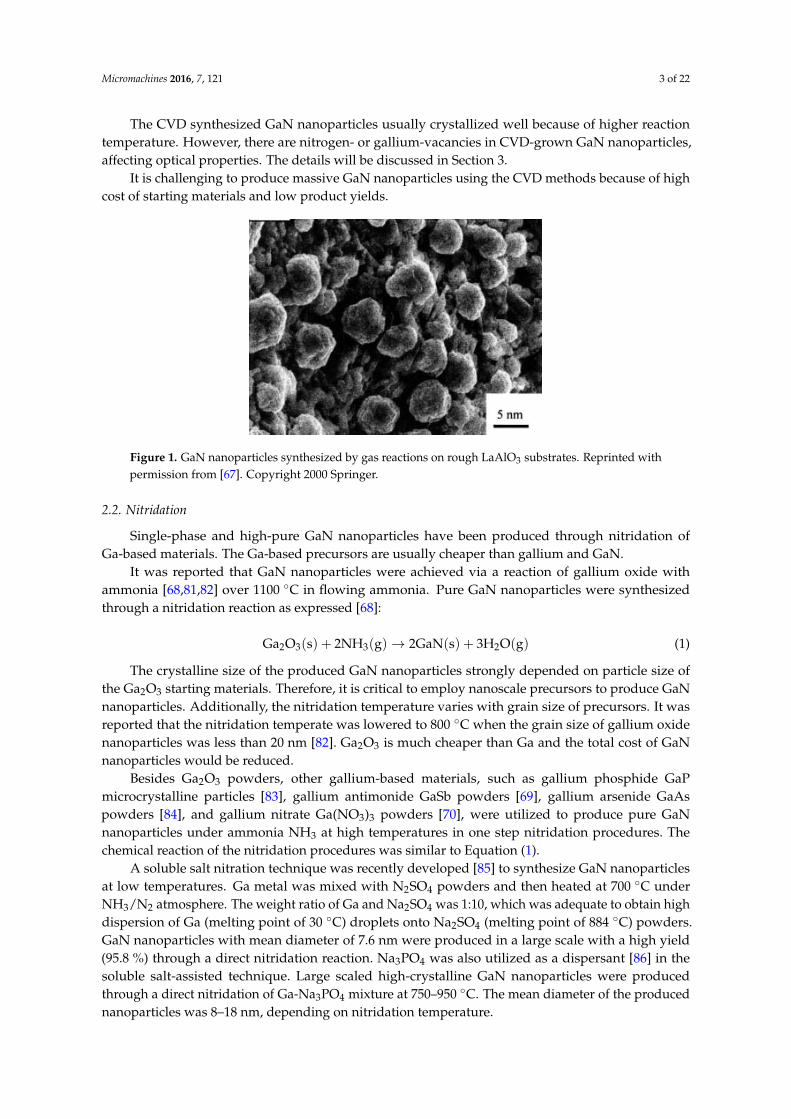
Ga vacancies always exist in GaN nanoparticles. Figure 2 shows a PL spectrum of GaNnanoparticles upon excitation at 325 nm recorded at room temperature. The diameter of thenanoparticles was 100–200 nm and the Ga/N ratio was 0.90. The spectrum exhibited three distinctfeatures: a blue emission at 413 nm coming from the free excitonic transition between valence andconduction bands of stoichiometric GaN, a broad blue luminescence (GL) centered at 467 nm, anda yellow luminescence (YL) band emission centered at 516 nm. The YL peak around 516 nm wassaturated easily with excitation intensity, indicating the YL band should be attributed to Ga vacancy atsurfaces [111]. The GL band at 467 nm showed almost no saturation, implying the band was related toisolated Ga vacancy (VGa).
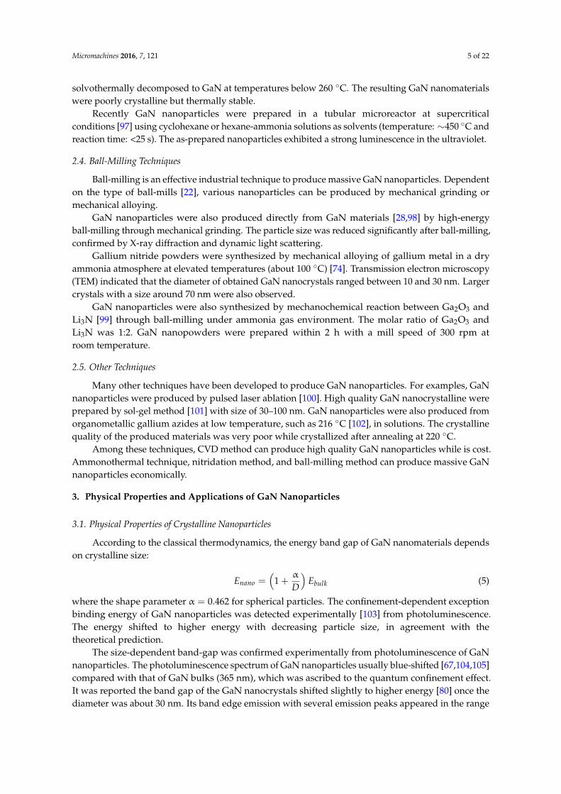
More detailed experiments showed that the optical absorption edge moved to longer wavelengths(red-shifted) as the concentration of Ga vacancies increased [112]. Figure 3 shows the effect of Gavacancy on UV-vis spectrum of GaN nanoparticles. The band-gap of GaN nanoparticles increased withdecreasing concentration of Ga vacancy. The band-gap of Ga0.90N nanparticles with the concentration

Micromachines 2016, 7, 121 7 of 22
of Ga vacancy of 2.8 % was 3.15 eV, 3.17 eV for Ga0.95N nanoparticles with the concentration of Gavacancy of 1.8%, and 3.20 eV for Ga0.98N nanoparticles with the concentration of Ga vacancy of1.6% [112].
Figure 2. Room-temperature photoluminescence spectrum of GaN nanoparticles with the Ga/N ratioof 0.90. Reprinted with permission from [112]. Copyright 2014 Springer.
Ga0.90NGa0.95NGa0.98N
Figure 3. UV-vis spectra of three GaN samples with different concentrations of Ga vacancies. Reprintedwith permission from [112]. Copyright 2014 Springer.
Nitrogen vacancies were observed in some GaN nanoparticles synthesized under nitrogen-absenceenvironments [113]. The dielectric properties of these N-deficient GaN nanoparticles exhibitedsignificant enhancement over that of GaN nanomaterials at low frequency range.
Doping can induce various defects in GaN nanoparticles and affect optical, magnetic properties.Here we do not discuss it.
Surface defects also affect photoluminescence [32,114]. Similar to Ga vacancies or nitrogenvacancies just discussed, the surface defects changed band gaps and shifted optical absorption edgesof GaN nanoparticles.
Surface defects also affect magnetic properties of GaN nanomaterials. GaN bulks are diamagnetic.However, un-doped GaN nanoparticles showed ferromagnetic at room temperature [115] when theaverage diameter of the nanoparticles was in the range 10–25 nm. Furthermore, the saturation magneticmoment decreased with increasing nanoparticles size, suggesting that ferromagnetism was due to thesurface defects of the nanoparticles. Recently experiments indicated the ferromagnetism should beinduced by Ga vacancies [112].

Micromachines 2016, 7, 121 8 of 22
Among two-dimensional defects of GaN nanoparticles, grain boundaries play a more importantrole than stacking faults, twins and inversion domain boundaries. The effects of grain boundariescan be described as the size effect and surface defects, as discussed above. Their effects on opticalproperties can be described by Equation (5).
Dislocations in GaN materials have played an important role of optical properties, especially forGaN films and GaN bulks. Here the effect is not discussed because the one-dimensional defects do notdominate physical properties of GaN nanoparticles.
Three-dimensional defects, such as voids, cracks and nanopipes are usually observed in bulksand films. However, this kind of defects is rarely observed in nanoparticles and not discussed here.
More detailed information of luminescence properties of defects in GaN can be found in previousreview literatures [116].
3.4. Applications of Nanoparticles
GaN nanoparticles have been deposited on substrates as solar cells [117]. The conversion efficiencyis 3.10 % under air mass 1.5 global illumination and room temperature conditions. A further increaseof 15 % was achieved in short circuit current density, improving the conversion efficiency to 3.87 %, inan optimized structure.
GaN nanoparticles with size of 15–20 nm were added to poly(3-hexylthiophene) (P2HT) as hybridsolar cells [118]. With the addition of GaN nanoparticles to P3HT from 5 mg/mL to 15 mg/mL, theperformance of the hybrid solar cells was greatly enhanced. The short circuit current density wastripled to 3.5 mA/cm2 and filling factor to 44% from 20%.
GaN nanoparticles were employed as photocatalysts for overall water splitting [119]. Thephotocatalytic activity of GaN for the reaction was found to be strongly dependent on the crystallinityof GaN nanoparitcles.
Compared to bulk materials, GaN nanoparticles have larger surface area, size-dependentproperties, increased absorption coefficient, increased band-gap energy, and reduced carrier-scatteringrate, offering potential advantages than bulks and films.
4. Free-standing Self-assembly of GaN Nanoparticles
GaN nanoparticles were self-assembled into various 2D macroscale structures on substrates,working as LEDs and LDs. 3D free-standing structures, such as porous nanotube arrays [120] andcrystalline nanotube arrays [43,121] were also fabricated by templates. Here we focus on free-standingGaN porous materials grown without any templates.
4.1. GaN Nanospheres
Figure 4 shows a GaN nanosphere [122] with a diameter of 20–25 nm. The nanosphere wasself-assembled from GaN nanoparticles with a diameter of several nanometers. It was believedthat there were lots of gallium nanodroplets around gallium sources. When ammonia NH3 gaswas introduced into reaction chambers, NH3 molecules were easily adsorbed onto surfaces of thenanosized gallium droplets. Then GaN nanoparticles nucleated at the surfaces of the metallic galliumnanodroplets. With increasing reaction time, more and more NH3 passed though the previouslyformed GaN-Ga interfaces to react with Ga to form GaN shells. Hollow spheres were formed when thegallium nanodroplets were consumed. The produced hollow spheres were composed of polycrystallinenanoparticles.
Sometimes the hollow GaN spheres further aggregated into columns, as shown in Figure 5.

Micromachines 2016, 7, 121 9 of 22
ing hollow GaN nanospheres by carefully controlling thetreatment temperature and the ammonia gas partial pres-sure. In the synthesis process, the nanosized Ga liquid drop-lets are first deposited on a silicon or sapphire substrateusing GaCl3 as gallium precursor, and the hollow GaNspheres are subsequently grown by an in situ chemical reac-tion between the liquid Ga formed and introduced NH3 inwhich the gallium droplets do not act as a catalyst, as re-ported previously,[25] but rather act as a reactant and a tem-plate for the formation of hollow GaN structures. Typically,the diameter of the synthesized hollow GaN spheres andnanotubes is 20–25 nm and the shell thickness of the hollowGaN nanostructures is 3.5–4.5 nm. The room-temperaturephotoluminescence spectra for the synthesized GaN spheresand nanotubes display a strong, blue-shifted band-edgeemission peak at 3.52 eV (352 nm).
2. Results and Discussion
After the synthesis a yellow bulk product collected onthe silicon substrate where the zone temperature was mea-sured to be 650 8C. The as-prepared products were charac-terized by X-ray diffraction. Figure 1a shows a typical XRD
spectrum from the synthesized product. The reflectionpeaks could be indexed to wurtzite GaN with lattice param-eters of a=3.186 @ and c=5.178 @ (JCPDS: 02-1078). Noother impurities could be indexed from the synthesizedproducts.
The synthesized products were sonicated in ethanol anddispersed onto copper grids coated with an amorphouscarbon film to carry out a transmission electron microscopy(TEM) examination of the morphologies and structures ofthe resulted products. Figure 2a and b show low-magnifica-tion TEM images of the synthesized hollow spherical parti-cles. They display pale regions in the central parts that con-trast with the dark shells or edges. When the sample wascontinuously tilted, the light contrast in the central part didnot vary in contrast and size. This excludes the possibility ofsolid spheres and suggests the hollow nature of the synthe-
sized GaN particles. Figure 2c depicts a high-magnificationTEM image of a typical single hollow sphere particle. Acontrast difference between the shell section and center ofthe particle can be observed, clearly indicating the hollowstructural nature of the synthesized product. Figure 2d is atypical selected-area electron diffraction (ED) pattern froman as-synthesized hollow sphere. The diffraction rings in theED pattern correspond well with that of wurtzite-type GaN,directly indicating that the spherical particle is composed ofpolycrystalline GaN with a wurtzite structure. Typically, thesynthesized hollow spheres are relatively uniform in size,ranging from 20 to 25 nm in diameter.
A high-resolution transmission electron microscope(HRTEM) attached to an X-ray energy dispersive spectrom-eter (EDS) were used to further characterize the synthe-sized hollow spheres both microstructurally and chemically.Figures 3a and b show two HRTEM images for the shells oftwo different hollow spheres. The shell section and core sec-tion of the synthesized hollow sphere can clearly be seen,and also that the shell of the hollow spheres is very thin andcomposed of very small nanoparticles. The thickness of theshell is in the range 3.5–4.5 nm. The inset in Figure 3a is theEDS spectrum obtained from the synthesized hollowsphere; it shows that the hollow sphere is composed of Gaand N, with a chemical composition of 1:0.99 (Ga:N ratio)corresponding to the expected stoichiometry of bulk GaN.The Cu signals come from the copper grid. It should benoted that several tens of hollow GaN spheres were charac-
Figure 1. XRD spectra of a) GaN hollow spheres, and b) GaN hollownanotubes.
Figure 2. a) Low- and b) high-magnification TEM images of the syn-thesized hollow spherical particles. c) A magnified TEM image of asingle hollow spherical particle. d) Selected-area electron diffraction(ED) pattern from a synthesized hollow sphere suggesting the syn-thesized hollow sphere is composed of polycrystalline GaN with awurtzite structure.
small 2005, 1, No. 11, 1094– 1099 ? 2005 Wiley-VCH Verlag GmbH&Co. KGaA, D-69451 Weinheim www.small-journal.com 1095
Semiconductor GaN Hollow Spheres and Nanotubes
Figure 4. HRTEM image of a GaN nanosphere. Reprinted with permission from [122]. Copyright 2005WILEY-VCH Verlag GmbH & Co.
tion of hollow GaN spheres. This process is similar to thatof InP quantum nanostructure growth by the in situ reactionof indium droplets with phosphide ions.[27] When the NH3
gas is introduced, because the surface area of the nanocrys-tals is much larger than that of the bulk materials, and thereare a lot of vacancies and dangling bonds on the surface ofthe Ga liquid droplets, the NH3 molecules are easily adsor-bed onto the surface of the starting nanosized Ga liquiddroplets. The surface of the metallic gallium liquid dropletis the location where GaN nucleates. NH3 reacts with galli-um to form GaN on the surface of the Ga droplets. With in-creasing time, more and more NH3 passes though the previ-ously formed GaN–liquid Ga interface to react with Ga andform GaN to finally give hollow spheres composed of small,polycrystalline particles. The formation process of hollowGaN spherical nanocrystals is shown schematically in Fig-ures 5a–c. As the Ga droplet serves as a template and a re-actant it strictly limits the lateral growth of individualhollow GaN spherical nanocrystals. The formation of hollowGaN nanotubes at higher temperature is easy to understandas at these temperatures the formed hollow GaN spheresaggregate, and the hollow GaN nanotubes could be formedby the coalescence of the nanosized hollow GaN spheres, asillustrated schematically in Figures 5d and e. The formationprocess of hollow GaN nanospheres is very similar to thatof ZnO shells reported by Wang et al.[28] Figure 6 showssome aligned hollow GaN spheres with diameters of 20–25 nm, and the hollow GaN polycrystalline nanotubes couldbe formed by the combination of such hollow spheres, thediameter of the hollow GaN nanotubes basically dependingon that of the hollow GaN spheres. The process for the for-mation of GaN nanotubes from hollow spheres is similar tothat of Co3O4 nanotubes from colloidal particles reported
by Shi et al.[29] Both the shell thickness of the hollowspheres and the wall thickness of the nanotubes are in therange 3–5 nm, and the synthesized products have a uniformsize distribution.
Figure 7 depicts a typical room-temperature PL spec-trum for the as-synthesized hollow GaN spheres, and almostthe same PL spectrum is obtained for the synthesized GaNnanotubes. Bulk GaN shows a band-edge emission at3.40 eV (365 nm). The PL spectrum of the synthesizedhollow GaN spheres displays a sharp emission peak, namelyan ultraviolet (UV) near-band-edge transition, at 3.52 eV(352 nm). The observed strong band-edge emission at3.52 eV (352 nm) is blue-shifted relative to that of bulkGaN by about 120 meV (13 nm). This should be attributedto a quantum confinement effect, because the synthesized
Figure 5. A schematic illustration of the formation process of hollowGaN spheres and hollow nanotubes: a) Generation of nanosizedliquid Ga droplets; b) GaN nanocrystal nucleation and growth on thesurface of Ga liquid droplets; c) the hollow GaN sphere is formedwith small shell size; d,e) at high temperatures the formed hollowGaN spheres aggregate and hollow GaN nanotubes are formed bythe coalescence of the nanosized hollow GaN spheres.
Figure 6. A TEM image of the aligned hollow GaN spheres; hollowGaN nanotubes could be formed by combination of these hollowGaN spheres.
Figure 7. The room-temperature photoluminescence (PL) spectrum ofthe synthesized hollow GaN spheres.
small 2005, 1, No. 11, 1094– 1099 ? 2005 Wiley-VCH Verlag GmbH&Co. KGaA, D-69451 Weinheim www.small-journal.com 1097
Semiconductor GaN Hollow Spheres and Nanotubes
Figure 5. TEM image a GaN sphere column. Reprinted with permission from [122]. Copyright 2005WILEY-VCH Verlag GmbH & Co.
4.2. GaN Nanotubes
GaN porous nanotubes were self-assembled from GaN nanoparticles [122]. Figure 6a showsseveral GaN nanotubes. The darker edges indicated that the GaN materials were hollow tubes, notsolid rods. The wall thicknesses were 3.5–5.0 nm. The GaN nanotubes had a length of several hundredsof nanometers. Selected area electron diffraction (SAED) patterns (inset of Figure 6b) indicated thatthe nanotubes were polycrystalline. Figure 6b shows detailed nanostructures of the nanotubes. Thenanotube walls were composed of single-layer-ed GaN nanocrystalline particles with a diameter of3.0–3.5 nm.
It was believed that the hollow GaN nanotubes were formed by the coalescence of the nanosizedhollow GaN columns shown in Figure 5.

Micromachines 2016, 7, 121 10 of 22
(a)
terized by EDS and the same results were obtained for allof them. The synthesized hollow GaN sphere is very stableeven under strong electron beam irradiation. To the best ofour knowledge, such hollow GaN spheres with a shell thick-ness of 3.5–4.5 nm have never been reported.
The products obtained could be controlled by carefullyadjusting the synthesis temperature at a given ammonia par-tial pressure. When we increased the treatment temperature,hollow nanotubes could be synthesized on the silicon sub-strate where the temperature was measured to be 700 8C.The XRD pattern for the synthesized GaN nanotubes isgiven in Figure 1b, suggesting the product is wurtzite-typeGaN. Figures 4a and b show low-magnification TEMimages of the hollow nanotubes obtained. The contrast dif-ference between the pore section and the wall section canclearly be seen, suggesting the tubular nature of the synthe-sized products. The synthesized nanotubes are typically 20–25 nm in outer diameter and the wall thickness of the tubesis 3.5–5.0 nm. Figure 4d is a SAED pattern obtained from asingle nanotube, suggesting that the synthesized nanotube ispolycrystalline with a wurtzite-type GaN structure. Fromthe HRTEM image obtained from the wall of a single GaNnanotube (Figure 4c), it can clearly be seen that the nano-tube wall is composed of small nanocrystals with a diameterof 3–3.5 nm.
The formation of the hollow GaN spherical nanostruc-tures is proposed to be a process composed of the followingstages: 1) generation of small, nanosized liquid Ga dropletson the substrate, 2) surface nitridation of Ga droplets, and3) a continuous in situ liquid gallium–NH3 gas interface re-action. Based on the starting materials, the yields of GaNhollow nanospheres and nanotubes obtained at differentsynthesis temperatures are about 37% and 32%, respective-ly. It should be noted that during the first stage, the initialdeposition and formation of nanosized Ga liquid particlesor droplets on the Si or sapphire substrate is of great impor-tance for the final formation of hollow GaN spheres. GaCl3has a melting point of 351 K and a boiling point of 473 K.Under thermal heating, the GaCl3 is vaporized and transfer-red by the Ar gas to the low-temperature zone. The Gaformed by decomposition of the GaCl3 deposits on the sili-con substrate. Ga has a low melting point of 302.8 K and aboiling point of 2520 K, therefore large amounts of Galiquid droplets form on the silicon or sapphire substrate.This is also supported by the Sacilotti groupKs recent reportof three-dimensional (3D) Ga balloon formation on a sili-con substrate.[26] During the subsequent GaN formationstage, the Ga liquid droplets or balloons do not act as a cat-alyst but rather as a reactant and a template for the forma-
Figure 3. a,b) High-resolution transmission electron microscopy(HRTEM) images of the shell of two hollow GaN spheres. The inset in(a) is the EDS spectrum of the shell of a hollow GaN sphere.
Figure 4. a) Low- and b) high-magnification TEM images of the hollowGaN nanotubes synthesized at a temperature above 1100 8C. c) AnHRTEM image taken from the wall of a single nanotube. The inset isa SAED pattern of a single nanotube, suggesting that the synthesizednanotube is polycrystalline.
1096 www.small-journal.com ? 2005 Wiley-VCH Verlag GmbH&Co. KGaA, D-69451 Weinheim small 2005, 1, No. 11, 1094 – 1099
full papers L.-W. Yin et al.
40 nm(b)
terized by EDS and the same results were obtained for allof them. The synthesized hollow GaN sphere is very stableeven under strong electron beam irradiation. To the best ofour knowledge, such hollow GaN spheres with a shell thick-ness of 3.5–4.5 nm have never been reported.
The products obtained could be controlled by carefullyadjusting the synthesis temperature at a given ammonia par-tial pressure. When we increased the treatment temperature,hollow nanotubes could be synthesized on the silicon sub-strate where the temperature was measured to be 700 8C.The XRD pattern for the synthesized GaN nanotubes isgiven in Figure 1b, suggesting the product is wurtzite-typeGaN. Figures 4a and b show low-magnification TEMimages of the hollow nanotubes obtained. The contrast dif-ference between the pore section and the wall section canclearly be seen, suggesting the tubular nature of the synthe-sized products. The synthesized nanotubes are typically 20–25 nm in outer diameter and the wall thickness of the tubesis 3.5–5.0 nm. Figure 4d is a SAED pattern obtained from asingle nanotube, suggesting that the synthesized nanotube ispolycrystalline with a wurtzite-type GaN structure. Fromthe HRTEM image obtained from the wall of a single GaNnanotube (Figure 4c), it can clearly be seen that the nano-tube wall is composed of small nanocrystals with a diameterof 3–3.5 nm.
The formation of the hollow GaN spherical nanostruc-tures is proposed to be a process composed of the followingstages: 1) generation of small, nanosized liquid Ga dropletson the substrate, 2) surface nitridation of Ga droplets, and3) a continuous in situ liquid gallium–NH3 gas interface re-action. Based on the starting materials, the yields of GaNhollow nanospheres and nanotubes obtained at differentsynthesis temperatures are about 37% and 32%, respective-ly. It should be noted that during the first stage, the initialdeposition and formation of nanosized Ga liquid particlesor droplets on the Si or sapphire substrate is of great impor-tance for the final formation of hollow GaN spheres. GaCl3has a melting point of 351 K and a boiling point of 473 K.Under thermal heating, the GaCl3 is vaporized and transfer-red by the Ar gas to the low-temperature zone. The Gaformed by decomposition of the GaCl3 deposits on the sili-con substrate. Ga has a low melting point of 302.8 K and aboiling point of 2520 K, therefore large amounts of Galiquid droplets form on the silicon or sapphire substrate.This is also supported by the Sacilotti groupKs recent reportof three-dimensional (3D) Ga balloon formation on a sili-con substrate.[26] During the subsequent GaN formationstage, the Ga liquid droplets or balloons do not act as a cat-alyst but rather as a reactant and a template for the forma-
Figure 3. a,b) High-resolution transmission electron microscopy(HRTEM) images of the shell of two hollow GaN spheres. The inset in(a) is the EDS spectrum of the shell of a hollow GaN sphere.
Figure 4. a) Low- and b) high-magnification TEM images of the hollowGaN nanotubes synthesized at a temperature above 1100 8C. c) AnHRTEM image taken from the wall of a single nanotube. The inset isa SAED pattern of a single nanotube, suggesting that the synthesizednanotube is polycrystalline.
1096 www.small-journal.com ? 2005 Wiley-VCH Verlag GmbH&Co. KGaA, D-69451 Weinheim small 2005, 1, No. 11, 1094 – 1099
full papers L.-W. Yin et al.
Figure 6. (a) Typical TEM image of GaN nanotubes synthesized above 1100 ◦C by a gas interfacereaction route; (b) Cross-sectional HRTEM image of a nanotube. The inset is an SAED pattern of thenanotube. Reprinted with permission from [122]. Copyright 2005 Wiley-VCH Verlag GmbH & Co.
4.3. GaN Circular Microtubes
Figure 7 shows wurtzite GaN microtubes grown by a CVD method without templates [123].Gallium was placed on quartz substrates in a hot-walled CVD system. Then Ga reacted with ammoniaat 820–840 ◦C and yellow GaN nanostructures were produced on the quartz substrates. Scanningelectron microscopy (SEM) indicated that the yellow deposits were microtubes (Figure 7a). Thediameter of the hollow microtubes was about 8 µm and lengths up to 100 µm. The ends of most ofthese microtubes were open, but some were closed (Figure 7b–d).
(a)
30 µm
(b)
áá
10 µm
áá
(c)
10 µm
áá á
(d)
10 µm
(e)
1 µmá
áá
(f)
0 5 1 0 1 5 2 00
2
4
6
8
1 0
1 2
Count
s
D i a m e t e r ( m i c r o n )
Figure 2: SEM images of (a-d) microtubules grown at different regions and (e) wall surface of
a microtubule. White arrows mark the closed ends, black arrows the open ends, and the blue
arrows the nanopores of the microtubules. (f) Histogram of microtubule diameter.
5
Figure 7. SEM images of (a–d) GaN microtubes grown on quartz substrates and (e) surface ofa microtube. White arrows mark the closed ends, black arrows the open ends, and blue arrowsthe nanopores of the microtubes; (f) Histogram of microtube diameter. Reprinted with permissionfrom [123]. Copyright 2015 Elsevier.

Micromachines 2016, 7, 121 11 of 22
The thicknesses of the microtube walls were roughly measured from the open ends of themicrotubes, about 100 nm. Detailed SEM examination (Figure 7e) indicated the walls were consistedof single layer of randomly oriented nanostructures. The diameters of the nanostructures were about100 nm and their lengths were about 1 µm.
SEM images (Figure 7e) also indicated that the thin walls of the microtubes were porous becauseof the random packing of the nanostructures. Some nanopores of these walls are notated by bluearrows in Figure 7e. Such porous microtubes should have large surface areas.
X-ray powder diffraction indicated that the microtubes were hexagonal GaN nanomaterials [123].The phase was also confirmed by SAED on TEM.
4.4. GaN Squared Microtubes
Squared GaN microtube were also synthesized by the CVD method [124], as shown in Figure 8a.The microtubes were several microns long. The thicknesses of the microtube walls were about 100 nm.More detailed SEM images (Figure 8b) indicated that the walls consisted of single layer of randomnanoparticles.
3 um
(a) (b)
Figure 8. SEM images of (a) a squared GaN microtube and (b) its surface. Reprinted with permissionfrom [124]. Copyright 2013 Springer.
Figure 9 shows a selected area electron diffraction (SAED) pattern taken from a nanoparticle ofthe squared microtubes. The nanoparticle was single crystalline. The SAED pattern had a three-foldsymmetry and was indexed as the cubic GaN phase with the space group of F43m along a zone axisof [111] (the lattice parameter a = 4.503 Å). Therefore, the squared microtubes should be consistedzinc-blende GaN nanoparticles.
[111]
Figure 9. SAED pattern of a nanoparticle consisting of squared GaN microtubes. Reprinted withpermission from [124]. Copyright 2013 Springer.

Micromachines 2016, 7, 121 12 of 22
The formation of the porous microtubules can be explained by the Liesegang phenominon anddiffusion limited growth. Large amounts of gallium liquid droplets condense on quartz substratesfrom gaseous gallium. Gallium nanodroplets evaporate at high temperatures to produce gallium vapor.Once ammonia passes the gallium nanodroplets, gallium vapor would react with ammonia to produceGaN nanoparticles (nanorods or irregular nanostructures). The number of the GaN nanoparticles perunit volume is so dense around the gallium droplets that the GaN nanoparticles can be considered as asupersaturated aerosol around the gallium droplets. These supersaturated GaN nanoparticles wouldspontaneously aggregate into Liesegang rings because of thermodynamatic stability [125,126]. GaNnanoparticle Liesegang rings were observed [124] and support the hypothesis.
Then porous GaN microtubules grow on the Liesegang rings. Based on the diffusion-limitedaggregation mechanism, the protruding parts of the GaN microrings would easily attract the GaNnanoparticles and grow quickly to build a new nanoparticle-wall from the Liesegang ring edges,leaving the hollow interior.
With the consuming of gallium, supersaturated GaN nanoparticles would be continuouslysynthesized from the reaction of ammonia and gallium vapor as long as the gallium vapor pressureare high enough, resulting in the continuous deposition of nanoparticles on the GaN microrings toform GaN microtubules. During the whole growth stage, the gallium droplets would evaporate togenerate the gallium vapor to keep the microtubules open or the microtubes would be closed if thegallium nano droplets were consumed before the experiments ended.
4.5. GaN Nanocomposite Bulks
GaN nanocomposite bulks were in-situ fabricated under ammonothermal conditions. TheGaN nanocomposite was directly produced through reactions of Ga metal and ammonia with NH4Clcatalysts in autoclaves [72]. Figure 10a shows a typical photograph of a fragment of the nanocomposites.The size of the fragment was about 0.7× 0.6 cm2 with an thickness of about 0.2 cm. The fragment wastransparent to visible light. SEM examinations revealed the existence of terrace steps which resemblecharacteristics of brittle materials. The assemblies were bulk materials like polycrystalline ceramicmaterials, not simple mechanical aggregation of grains.
(a)
Fig. 3. (a) TEM image of morphology of the nanosized grains in NAB GaN. (b) TEM powder electron di!raction patterns. (c) TEMnano area di!raction pattern on a single nanosized grain. (d) HRTEM image taken along [0 0 1] axis. (e) HRTEM image taken along[1 0 0] axis. (f ) HRTEM image showing a pore resulting from the packing of three grains of [0 0 1] orientation. The images wererecorded on a Hitachi H-9000 HRTEM.
X.L. Chen et al. / Journal of Crystal Growth 209 (2000) 208}212 211
(b)
Fig. 2. Powder X-ray di!raction pattern for the nanocrystal-assembled bulk GaN.
(Fig. 3c) on a single grain taken along the [0 0 1]axis gives further evidence that the nanosizedgrains are hexagonal GaN. Figs. 3d and e showtypical high-resolution transmission electronmicroscopy (HRTEM) images taken along [0 0 1]and [1 0 0] zone axes of two grains of 18 and 12 nmin size, respectively. It can be seen that thenanosized grains in the NAB GaN are well crystal-lized. The lattice constants calculated from thefringe spacings of (1 0 0) and (0 0 1) planes area"3.1 As and c"5.2 As , in good agreement withthe above values determined by powder X-ray dif-fraction pattern. The morphology of the atom clus-ters observed from HRTEM images along di!erentaxes indicates that the clusters are rather equiaxed.The NAB GaN also contains pores as in thenanophase materials formed by sintering or com-pacting nanosized powders. Fig. 3f shows HRTEMimages of a pore resulting from the packing of threegrains with [0 0 1] orientation. The size of thesepores is estimated to be around &5 nm, roughlyhalf of the average diameter of grains. The densityfor NAB GaN measured by Archimedes den-sitometry is 72% of that for the GaN single crys-tals. This value approaches the theoretical limit forclose packing of identical spheres. Since the size ofpores is well below the wavelengths of visible light,the NAB GaN is transparent to visible light. Occa-
sionally, opaque samples were obtained wheremuch larger pores were indeed observed.
The formation mechanism of NAB and nano-crystalline GaN is not clear. A similar method wasrecently reported to produce GaN microcrystalswith lithium, potassium compounds or rare earthelements as mineralizers [15]. In the present pro-cess, the addition of NH
4Cl is indispensable in
forming GaN at such a low temperature &3503C.A possible mechanism is proposed as follows.NH
4Cl is known to be very soluble in liquid am-
monia (124 g/100 g NH3) and the resulting solution
possesses a strong acidity [16]. Metal Ga maybe easily oxidised to produce Ga3` ions andform soluble intermediate compounds such asGa(NH
3)nCl
3(n"1}14) [16] in such a solution.
Then nano-sized GaN will precipitate from eitherthe decomposition or further reactions of theseintermediate compounds with liquid ammonia.Since there is a strong aggregating tendency fornanosized clusters in the solution like the case withsmall clusters in a colloid, these nanocrystals areconsolidated into NAB GaN when the pressure inan autoclave is high enough. Consolidation of ox-ide "ne particles was already known to be e!ectivein hydrothermal process [13].
In conclusion, nanocrystal-assembled bulk GaNwas synthesized by a one-step method. The bulk
210 X.L. Chen et al. / Journal of Crystal Growth 209 (2000) 208}212
(c)
Figure 10. (a) Optical photograph of a fragment of GaN nanocomposites. The grid spacingsare 0.2× 0.2 cm2; (b) HRTEM image of three adjacent nanograins; (c) An XRD pattern of GaNnanocomposites. Reprinted with permission from [72]. Copyright 2000 Elsevier.

Micromachines 2016, 7, 121 13 of 22
The GaN nanocomposite bulks were consisted of nanograins with several nanometers. Figure 10bshows an HRTEM image of three adjacent GaN nanograins with [001] orientation. Each adjacentnanograin was chemically bounded with others. Among the three adjacent nanograins, a nanoporewas generated. The size of these pores was around 5 nm, roughly half of the average diameter of grains.Since the size of pores was well below the wavelengths of visible light, the GaN nanocomposites wastransparent to visible light as shown in Figure 10a.
The exist of nanopores in the nanocomposites was indirectly confirmed by mass densitymeasurements. The measured mass density for the GaN nanocomposites was 72% of that for the GaNsingle crystals. This value approached the theoretical limit of close-packing of equal spheres.
Figure 10c shows the XRD pattern of the GaN nanocomposites. The XRD pattern indicated thatthe assembly was hexagonal GaN. All reflections were broadened due to the size effect. The averagegrain size was 11.8 nm according to the Scherrer formula, in agreement with HRTEM observation inFigure 10b.
The formation mechanism of GaN nanocomposites is not clear. A possible mechanism wasproposed as follows [72]: (1) NH4Cl is very soluble in liquid ammonia (124 g/100 g NH3) and theresulting solution possesses a strong acidity; (2) Metal gallium reacts with ammonia to produce Ga3+
ions and form soluble intermediate compounds such as Ga(NH3)nCl3 (n = 1− 14) [127] in such a acidicsolution; (3) Then nano-sized GaN particles would precipitate from either the decomposition or furtherreactions of these intermediate compounds with liquid ammonia; (4) There was a strong aggregatingtendency for nanosized clusters in the solution and the GaN nanocrystals were consolidated into GaNnanocomposites when the pressure in an autoclave is high enough.
5. Optical Properties of GaN Self-assemblies
The GaN self-assemblies talked here are consisted of nanoparticles whose optical propertiesstrongly depend on crystalline size. Their photoluminescence and Raman scattering are discussed inthis section.
5.1. Photoluminescence
Figure 11a shows a typical photoluminescence (PL) spectrum of an individual GaN circularmicrotube (Figure 7), excited by 532 nm wavelength radiation. The laser beam was focused onthe individual microtube under an optical microscope to excite the PL spectrum. A yellow band,centered at 653 nm, was observed. Similar yellow bands were also observed in nanoparticles [23] andnanowires [32] with wurtzite structure.
the consuming of gallium, supersaturated GaN nanorods are con-tinuously produced from the reaction of ammonia and gallium vaporas long as the gallium vapor pressure are high enough, resulting inthe continuous deposition of GaN nanorods on the GaN microringsto form GaN microtubules. During the whole growth stage, thegallium droplets evaporate to generate the gallium vapor to keep themicrotubules open.
The gallium droplet size is reduced with the reaction timebecause of evaporation. Once the gallium droplets vanish, the vaporpressure of the gallium droplets would decrease near the open endsof GaN tubules. As a result, the gallium vapor pressure front shouldshrink back from the microtubule open tips. Because the GaNnanorods aggregate along the gallium vapor pressure front, theaggregating GaN nanorod front would also shrink back to enclosethe microtubule ends, forming enclosed GaN microtubes as shown inFig. 6d. The SEM images in Fig. 6d show two microtubules with half-closed ends.
Additionally, the GaN microtubules are synthesized in a short time– only 2 min. It is the indirect evidence for the supersaturationgrowth, indicating rapidity of the Liesegang ring formation and themicrotubule growth. These two phenomena (ring formation andrapid growth) are the specific characteristics of super-saturationgrowth caused by the Liesegang effect.
4. Conclusion
One kind of novel gallium nitride circular tubules is grown fromwurtzite nanorods by chemical vapor deposition. The bottom-upgrownmicrotubules are porous, several tens of micrometers long andseveral microns in diameter. The constituent nanorods are crystallinewith lots of defects. The self-assembly of GaN nanomaterials iscontributed to the diffusion limited growth of supersaturated GaNnanorods. Compared with bulk crystals, the Raman active modes of
550 600 650 700 750 8000
5
10
15
20
Inte
nsity
(a.u
.)
Wavelength (nm)550 600 650 700 750 800
0
5
10
15
20
Inte
nsity
(a.u
.)
Wavelength (nm)
Fig. 5. Photoluminescence spectra of (a) a GaN circular microtube with wurtzite structure and (b) a GaN squared microtube with zinc-blende structure.
Initial Stage Template Stage Growth Stage Enclosing Stage
Ga
quartz
Ga
quartz quartz
: substrate
: Ga vapor
: Ga droplet
: Liesegang ring of GaN
: GaN nanorod
quartz
Fig. 6. Possible growth mechanism of the self-assembled GaN microtubules. (a) Initial stage. No GaN nanomaterials are synthesized. (b) Template stage. Liesegang rings ofGaN nanomaterials are formed. (c) Growth stage. GaN nanorods self-assemble into microtubules. (d) Enclosing stage. Ga sources are exhausted and the ends of GaNmicrotubules are closed. Top: model of each stage. Middle and bottom: SEM images at each stage.
Y. Lan et al. / Journal of Crystal Growth 415 (2015) 139–145 143
Figure 11. Photoluminescence spectra of (a) a GaN circular microtube with wurtzite structure and (b) aGaN squared microtube with zinc-blende structure. Reprinted with permission from [123]. Copyright2015 Elsevier.

Micromachines 2016, 7, 121 14 of 22
Figure 11b shows a PL spectrum of the square microtubes shown in Figure 8. A strong and wideyellow band was observed at 550–750 nm. It is generally accepted that nitrogen vacancies and deeplevel impurities contribute to the yellow band.
Figure 12 shows a typical room-temperature PL spectrum of GaN nanospheres shown in Figure 4.The PL spectrum of GaN hollow spheres displayed a sharp ultraviolet near-band-edge transition at3.52 eV (352 nm). The observed strong band-edge emission blue-shifted ∼ 120 meV relative to thatof bulk GaN (dashed curve in the figure, 3.40 eV). The blue-shift should be attributed to a quantumconfinement effect. A weak yellow luminescence transition was observed at 2.3 eV (539 nm) in the PLspectrum. The YL emission at 2.3 eV was located far below the band edge and was usually contributedto point defects within the GaN nanoparticles.
tion of hollow GaN spheres. This process is similar to thatof InP quantum nanostructure growth by the in situ reactionof indium droplets with phosphide ions.[27] When the NH3
gas is introduced, because the surface area of the nanocrys-tals is much larger than that of the bulk materials, and thereare a lot of vacancies and dangling bonds on the surface ofthe Ga liquid droplets, the NH3 molecules are easily adsor-bed onto the surface of the starting nanosized Ga liquiddroplets. The surface of the metallic gallium liquid dropletis the location where GaN nucleates. NH3 reacts with galli-um to form GaN on the surface of the Ga droplets. With in-creasing time, more and more NH3 passes though the previ-ously formed GaN–liquid Ga interface to react with Ga andform GaN to finally give hollow spheres composed of small,polycrystalline particles. The formation process of hollowGaN spherical nanocrystals is shown schematically in Fig-ures 5a–c. As the Ga droplet serves as a template and a re-actant it strictly limits the lateral growth of individualhollow GaN spherical nanocrystals. The formation of hollowGaN nanotubes at higher temperature is easy to understandas at these temperatures the formed hollow GaN spheresaggregate, and the hollow GaN nanotubes could be formedby the coalescence of the nanosized hollow GaN spheres, asillustrated schematically in Figures 5d and e. The formationprocess of hollow GaN nanospheres is very similar to thatof ZnO shells reported by Wang et al.[28] Figure 6 showssome aligned hollow GaN spheres with diameters of 20–25 nm, and the hollow GaN polycrystalline nanotubes couldbe formed by the combination of such hollow spheres, thediameter of the hollow GaN nanotubes basically dependingon that of the hollow GaN spheres. The process for the for-mation of GaN nanotubes from hollow spheres is similar tothat of Co3O4 nanotubes from colloidal particles reported
by Shi et al.[29] Both the shell thickness of the hollowspheres and the wall thickness of the nanotubes are in therange 3–5 nm, and the synthesized products have a uniformsize distribution.
Figure 7 depicts a typical room-temperature PL spec-trum for the as-synthesized hollow GaN spheres, and almostthe same PL spectrum is obtained for the synthesized GaNnanotubes. Bulk GaN shows a band-edge emission at3.40 eV (365 nm). The PL spectrum of the synthesizedhollow GaN spheres displays a sharp emission peak, namelyan ultraviolet (UV) near-band-edge transition, at 3.52 eV(352 nm). The observed strong band-edge emission at3.52 eV (352 nm) is blue-shifted relative to that of bulkGaN by about 120 meV (13 nm). This should be attributedto a quantum confinement effect, because the synthesized
Figure 5. A schematic illustration of the formation process of hollowGaN spheres and hollow nanotubes: a) Generation of nanosizedliquid Ga droplets; b) GaN nanocrystal nucleation and growth on thesurface of Ga liquid droplets; c) the hollow GaN sphere is formedwith small shell size; d,e) at high temperatures the formed hollowGaN spheres aggregate and hollow GaN nanotubes are formed bythe coalescence of the nanosized hollow GaN spheres.
Figure 6. A TEM image of the aligned hollow GaN spheres; hollowGaN nanotubes could be formed by combination of these hollowGaN spheres.
Figure 7. The room-temperature photoluminescence (PL) spectrum ofthe synthesized hollow GaN spheres.
small 2005, 1, No. 11, 1094– 1099 ? 2005 Wiley-VCH Verlag GmbH&Co. KGaA, D-69451 Weinheim www.small-journal.com 1097
Semiconductor GaN Hollow Spheres and Nanotubes
Figure 12. The room-temperature photoluminescence spectrum of hollow GaN spheres. Dashed line:bulk GaN. Reprinted with permission from [122]. Copyright 2005 Wiley.
The PL spectrum of GaN nanotubes shown in Figure 6 was almost the same as that of GaNnanospheres.
Yellow bands were also observed in PL spectra of GaN nanocomposites [72]. The YL emissionshould come from the surface defects and vacancies of consisting GaN nanoparticles.
5.2. Raman Scattering
The space group of wurtzite GaN is C46v and two formula units are contained in its unit cell.
According to the factor group analysis, there are six Raman-active modes, 1 A1(TO) + 1 A1(LO) + 1E1(TO) + 1 E1(LO) + 2E2.
Figure 13 shows a typical Raman spectrum of a GaN circular microtubes shown in Figure 7.The laser beam was focused on one GaN microtube under an optical microscope and the Ramanspectrum was collected from the individual microtube. Among theoretically predicated six activeRaman modes, four active modes were observed from the self-assemblies. The peaks at 519, 544, 564,and 719 cm−1 corresponded to the A1(TO), E1(TO), E2(high), and A1(LO) symmetries, respectively.Compared with bulk data (532 cm−1 for A1(TO), 559 cm−1 for E1(TO), 568 cm−1 for E2(high), 734 cm−1
for A1(LO)), the four active Raman modes significantly red-shifted to shorter wavenumbers. Twoother Raman modes were observed on the low wavenumber side of the A1(LO) mode. The two peaksat 656 cm−1 and 704 cm−1 should be surface optical (SO) phonon modes corresponding to A1 andE1 symmetries respectively. The SO phonon modes should be caused by surface effects of the GaNnanorods. A unusual Raman peak was observed at 414 cm−1 (inset of Figure 13). The peak should bethe acoustic overtone from wurtzite GaN nanoparticles.
Table 2 compares the Raman modes of self-assembled GaN circular microtubes and GaNcrystalline bulks. All the Raman-active modes red-shifted compared with crystalline bulks. A1

Micromachines 2016, 7, 121 15 of 22
(TO), E1(TO), and A1(LO) modes of the self-assemblies shifted more than these of individualGaN nanoparticles.
Raman modes of other kinds of free-standing self-assemblies also shifted as the circular microtubes.
A PL spectrum of zinc-blende microtubes [47] is shown in Fig. 5bfor comparison. The PL spectrum of the zinc-blende microtubes iscentered at 685 nm. The PL spectrum of the circular microtubesblue-shifts to higher energy, reflecting the fact that the wurtzite GaNhas a wider band-gap (3.4 eV) than the cubic GaN (3.2 eV) [50].
Growth mechanism: The formation of the porous microtubulescan be explained by the Liesegang phenomenon [51] and diffusionlimited growth. Gallium has a low melting point of 303 K and aboiling point of 2520 K. Therefore, large amounts of gallium liquiddroplets can condense on quartz substrates from gaseous gallium(Fig. 6a), as observed on silicon substrates [52]. The diameter of
the condensed droplets is usually 5–50 μm [53], depending onreaction temperatures and substrates. The behavior of gallium isvery similar to that of other low melting point metals, such asselenium [17]. Gallium droplets evaporate at high temperatures toproduce gallium vapor during the CVD procedure. Once ammoniapasses the gallium droplets, gallium vapor would react withammonia to produce GaN nanoparticles (Fig. 6b). The number ofthe GaN nanoparticles per unit volume is so dense around thegallium droplets that the GaN nanoparticles around the galliumdroplets can be considered as a supersaturated aerosol, similar tocharged nanoparticles in solutions [54] and nanoparticles in vaporphases [55,56]. These supersaturated GaN nanoparticles wouldspontaneously aggregate into Liesegang rings due to thermody-namic stability, as observed in other kinds of ordered Liesegangnanoparticle-rings [54,57].
The proposed growth mechanism is experimentally confirmed bySEM observation. The middle panel in Fig. 6b shows an SEM image ofa typical GaN nanoparticle Liesegang ring with a diameter of severalmicrometers. A higher magnification SEM image (bottom panel inFig. 6b) indicates that the microring consists of many GaN nanopar-ticles with a size below 100 nm. Other size GaN rings are alsoobserved on the substrates. These surviving GaN Liesegang ringsindicate that the Liesegang rings can self-assemble from GaNnanomaterials during the CVD procedures when GaN nanoparticlesare supersaturated enough.
Then, porous GaN microtubules grow on the Liesegang ringtemplates, as shown in Fig. 6c. Based on the diffusion-limitedaggregation mechanism, the protruding parts of the GaN micror-ings can easily attract the GaN nanorods and grow quickly to buildnew nanorod-walls from the Liesegang ring edges, leaving thehollow interior. The SEM images in Fig. 6c show tips of two GaNmicrotubules, indicating the growth on the Liesegang rings. With
Distance (um) 0 1 2 3 4
I
nten
sity
(arb
. uni
t)
0 5 10 150
200
400
600
800
Inte
nsity
(cou
nts)
Energy (kV)
N
Ga
Cu
Ga
Cu Ga
Fig. 3. (a) BF-TEM image of a GaN microtubule. Several typical nanopores are marked by arrows. (b) EDS spectrum of the microtubule in (a). Cu signal coming from the TEMgrid. (c) SAED pattern of the microtubule in (a). (d) EDS linescan of Ga�Kα across the microtubule in (a). (e) BF-TEM image of several adjacent nanorods near a nanopore.(f) SAED of the nanorod circled in (e). (g) HRTEM image of the nanorod circled in (e). (h) IFFT of (g). Inset: FFT of (g). Two green circles mark the diffraction spots used for IFFT.(For interpretation of the references to color in this figure caption, the reader is referred to the web version of this paper.)
450 500 550 600 650 700 7500
5
10
15
20
25
400 500 600 700 800
0
10
20
30RamanIntensity(arb.u.)
Wavenumber (/cm)414/cm
Fig. 4. Raman scattering of a GaN microtubule. ○: experimental; : fitting. Inset:whole range of Raman scattering of the microtubule (red curve) compared withthat of GaN crystalline films (blue curve). (For interpretation of the references tocolor in this figure caption, the reader is referred to the web version of this paper.)
Y. Lan et al. / Journal of Crystal Growth 415 (2015) 139–145142
Figure 13. Room-temperature Raman scattering of a GaN circular microtubule. ◦: experimental; −−:fitting. Inset: whole range of Raman scattering of the microtube (red curve) compared with that of GaNcrystalline films (blue curve). Reprinted with permission from [123]. Copyright 2015 Elsevier.
Table 2. Raman scattering of hexagonal GaN materials.
Mode E2 (low) A1(TO) E1(TO) E2(high) SO(A1) SO(E1) A1(LO) E1(LO) Reference(cm−1) (cm−1) (cm−1) (cm−1) (cm−1) (cm−1) (cm−1) (cm−1)
crystals 144 533 561 569 - - 735 743 [128]nanoparticles † - 528 552 564 656 - 730 - [88]microtubes ‡ - 519 544 564 656 704 719 - [123]
SO: surface optical phonon mode. †: crystalline size: ∼12 nm. ‡: crystalline size: ∼100 nm.
6. Potential Applications of GaN Self-Assemblies
GaN self-assemblies of 1D nanomaterials (nanowires and nanorods) have been utilized asphotocatalytic water splitting [129,130], photovoltaic devices [131,132], piezoelectric nanogenerators [65],and light-emitting diodes [63]. Free-standing GaN self-assemblies of 0D nanoparticles have largersurface/volume ratios than these of the GaN 1D nanomaterials. So the reviewed free-standingnanoporous self-assemblies should have wider potential applications.
6.1. Photocatalytic Water Splitting
GaN semiconductors have been employed for photoelectrochemical water splitting [133–136]since 2005 [133,134] to generate hydrogen gas. Up to now, GaN nanowire arrays have been utilized togenerate hydrogen [129,130,137,138]. The highest incident-photon-to-current-conversion efficiency of15%–18% [138] was obtained . Nanoporous GaN films were also employed to split water [139]. Thenanoporous GaN films showed better efficiency and stability [139]. It was concluded that the largesurface area of the porous GaN enhanced hole transport from photoanode to electrolyte and resultedbetter photovoltaic performances.
It was believed [138] that GaN nanostructures possess large surface-to-volume ratios, surfacedefects, rapid charge carrier separation, and enhanced optical absorption, being a better candidate to

Micromachines 2016, 7, 121 16 of 22
split water. Free-standing GaN porous assemblies shown in Figures 8–10 have higher surface/volumeratio than all the reported nanowire/nanorod/nanoparticle arrays. Therefor a better photocatalyticperformance is expected for free-standing GaN self-assemblies.
6.2. Piezoelectric Nanogenerators
GaN nanowire arrays produced output voltage pulses when pressed [65]. Theoretical calculationpredicated [140] that piezoelectric constant of GaN nanomaterials increased with decreasing crystallinesize of nanomaterials while surface piezoelectric coefficient was constant.
Crystalline size of free-standing GaN self-assemblies is several nanometers in three-dimensions,smaller than GaN nanowires that are in nanoscale in two dimensions. Therefore, the free-standingGaN self-assemblies of nanoparticles should have better piezoelectric performances than GaNnanowire arrays.
6.3. Thermoelectric Devices
GaN possesses excellent electronic transport properties such as high charge carrier mobility to bethermoelectric materials. In a GaN nanocrystalline ceramic prepared by hot pressing, a reasonablylarge Seebeck coefficient, S, of −58 µV/K was reported at room temperature [141]. As self-assemblyis a promising method for making nanostructured materials in situ, with proper optimization, theself-assembly materials hold promise for high efficiency downscaled thermoelectric devices [142].
Potential thermoelectric applications of the GaN-based low dimensional nanomaterials that areformed by self-assembly techniques are of great interest because of the possibility to be shaped intodevices and circuits, and because of the potential for direct integration of microcooler/power generatorswith various electronic devices. Although to date there have not been reports on thermoelectricapplications of self-assembled GaN and GaN-based nanomaterials, it is hoped that information on theimproved thermoelectric properties of doped GaN-based bulk and low-dimensional nanomaterialspresent here may stimulate such development.
6.4. Other Potential Applications in Renewable Energy
GaN self-assemblies reviewed here are nanoporous and consisted of nanoparticles, holding noveloptical properties. This kinds of nanomaterials should also have applications in batteries, capacitors,and solar cells. However, it is difficulty to massively produce such kinds of porous nanostructures. Fewresearches on renewable energy have been reported. More potential applications of the free-standingnanoporous nanomaterials are expected in the coming years.
7. Conclusions
The syntheses and physical properties of hexagonal GaN nanoparticles are briefly reviewed.These novel GaN nanoparticles can be self-assembled into free-standing nanospheres, nanotubes,microtubes, and composite bulks without any templates. The mechanism and physical properties ofthese self-assemblies are discussed. The potential applications of the assemblies are expected based ontheir high surface/volume ratios and tunable band-gaps.
Acknowledgments: The author YL acknowledges the financial support by the Defense Threat Reduction Agencyunder Grant HDTRA122221, the support from US Department of Energy under the Contract DE-NA0000720through the program of S. P. Massie Chair of Excellence.
Author Contributions: Jianye Li contributed to nanoparticles, Yucheng Lan and Abdellah Lisfi to selfassemblies,Winnie Wong-Ng drafted potential applications, Rola M. Derbeshi collected references, Yucheng Lan and Jiang Licontributed to organization of the review and potentials in renewable energy.
Conflicts of Interest: The authors declare no conflict of interest.

Micromachines 2016, 7, 121 17 of 22
References
1. Morkoç, H.; Strite, S.; Gao, G.B.; Lin, M.E.; Sverdlov, B.; Burns, M. Large band gap SiC, III-V nitride, andII-VI ZnSe-based semiconductor device technologies. J. Appl. Phys. 1994, 76, 1363–1398.
2. Mohammad, S.; Morkoç, H. Progress and prospects of group-III nitride semiconductors. Prog. Quant. Electron.1996, 20, 361–525.
3. Akasaki, I.; Amano, H. Crystal Growth and Conductivity Control of Group III Nitride Semiconductors andTheir Application to Short Wavelength Light Emitters. Jpn. J. Appl. Phys. 1997, 36, 5393.
4. Nakamura, S. The Roles of Structural Imperfections in InGaN-Based Blue Light-Emitting Diodes and LaserDiodes. Science 1998, 281, 956–961.
5. Chen, X.L.; Lan, Y.C.; Liang, J.K.; Cheng, X.R.; Xu, Y.P.; Xu, T.; Jiang, P.Z.; Lu, K.Q. Structure and HeatCapacity of Wurtzite GaN from 113 to 1073 K. Chin. Phys. Lett. 1999, 16, 107–108.
6. Monemar, B. Fundamental energy gap of GaN from photoluminescence excitation spectra. Phys. Rev. B1974, 10, 676–681.
7. Korona, K.P.; Wysmołek, A.; Pakuła, K.; Stepniewski, R.; Baranowski, J.M.; Grzegory, I.; Łucznik, B.;Wróblewski, M.; Porowski, S. Exciton region reflectance of homoepitaxial GaN layers. Appl. Phys. Lett. 1996,69, 788–790.
8. Nakamura, S.; Mukai, T.; Senoh, M. High-Power GaN P-N Junction Blue-Light-Emitting Diodes. Jpn. J.Appl. Phys. 1991, 30, L1998.
9. Nakamura, S.; Senoh, M.; Mukai, T. High-power InGaN/GaN double-heterostructure violet light emittingdiodes. Appl. Phys. Lett. 1993, 62, 2390–2392.
10. Ponce, F.A.; Bour, D.P. Nitride-based semiconductors for blue and green light-emitting devices. Nature 1997,386, 351–359.
11. Akasaki, I.; Amano, H.; Sota, S.; Sakai, H.; Tanaka, T.; Koike, M. Stimulated Emission by Current Injectionfrom an AlGaN/GaN/GaInN Quantum Well Device. Jpn. J. Appl. Phys. 1995, 34, L1517.
12. Amano, H.; Asahi, T.; Akasaki, I. Stimulated Emission Near Ultraviolet at Room Temperature from a GaNFilm Grown on Sapphire by MOVPE Using an AlN Buffer Layer. Jpn. J. Appl. Phys. 1990, 29, L205.
13. Asif Khan, M.; Kuznia, J.N.; Bhattarai, A.R.; Olson, D.T. Metal semiconductor field effect transistor based onsingle crystal GaN. Appl. Phys. Lett. 1993, 62, 1786–1787.
14. Brandt, M.S.; Herbst, P.; Angerer, H.; Ambacher, O.; Stutzmann, M. Thermopower investigation of n- andp-type GaN. Phys. Rev. B 1998, 58, 7786 – 7791.
15. Liu, W.; Balandin, A.A. Thermoelectric effects in wurtzite GaN and AlxGa1−xN alloys. J. Appl. Phys. 2005,97, 123705.
16. Adachi, S. Lattice thermal conductivity of group-IV and III-V semiconductor alloys. J. Appl. Phys. 2007,102, 063502.
17. Hurwitz, E.; Asghar, M.; Melton, A.; Kucukgok, B.; Su, L.; Orocz, M.; Jamil, M.; Lu, N.; Ferguson, I.Thermopower Study of GaN-Based Materials for Next-Generation Thermoelectric Devices and Applications.J. Electron. Mater. 2011, 40, 513–517.
18. Lu, M.; guang Zhang, G.; Fu, K.; hao Yu, G.; Su, D.; feng Hu, J. Gallium Nitride Schottky betavoltaic nuclearbatteries. Energ. Convers. Manag. 2011, 52, 1955–1958.
19. Cheng, Z.; Chen, X.; San, H.; Feng, Z.; Liu, B. A high open-circuit voltage gallium nitride betavoltaicmicrobattery. J. Micromech. Microeng. 2012, 22, 074011.
20. San, H.; Yao, S.; Wang, X.; Cheng, Z.; Chen, X. Design and simulation of GaN based Schottky betavoltaicnuclear micro-battery. Appl. Radiat. Isot. 2013, 80, 17–22.
21. Li, J.; Li, F.; Lin, S.; Zhong, S.; Wei, Y.; Meng, X.; Shen, X. Theoretical study on InxGa1−xN/Si hetero-junctionsolar cells. Proc. SPIE 2009, 7409, 740910.
22. Lan, Y.; Ren, Z. Nanomaterials for Sustainable Energy; Springer-Verlag: New York, NY, USA, 2016; ChapterThermoelectric Nanocomposites for Thermal Energy Conversion, pp. 371–443.
23. Lan, Y.C.; Chen, X.L.; Xu, Y.P.; Cao, Y.G.; Huang, F. Syntheses and structure of nanocrystalline galliumnitride obtained from ammonothermal method using lithium metal as mineralizator. Mater. Res. Bull. 2000,35, 2325–2330.
24. Han, W.; Fan, S.; Li, Q.; Hu, Y. Synthesis of Gallium Nitride Nanorods through a Carbon Nanotube-ConfinedReaction. Science 1997, 277, 1287–1289.

Micromachines 2016, 7, 121 18 of 22
25. Kim, H.M.; Kim, D.; Park, Y.; Kim, D.; Kang, T.; Chung, K. Growth of GaN Nanorods by a Hydride VaporPhase Epitaxy Method. Adv. Mater. 2002, 14, 991–993.
26. Deb, P.; Kim, H.; Rawat, V.; Oliver, M.; Kim, S.; Marshall, M.; Stach, E.; Sands, T. Faceted and VerticallyAligned GaN Nanorod Arrays Fabricated without Catalysts or Lithography. Nano Lett. 2005, 5, 1847–1851.
27. Xiang, X.; Zhu, H. One-dimensional gallium nitride micro/nanostructures synthesized by a space-confinedgrowth technique. Appl. Phys. A Mater. Sci. Process. 2007, 87, 651–659.
28. Li, J.Y.; Chen, X.L.; Qiao, Z.Y.; Cao, Y.G.; Lan, Y.C. Formation of GaN nanorods by a sublimation method.J. Cryst. Growth 2000, 213, 408–410.
29. Han, W.; Redlich, P.; Ernst, F.; Rühle, M. Synthesis of GaN-carbon composite nanotubes and GaN nanorodsby arc discharge in nitrogen atmosphere. Appl. Phys. Lett. 2000, 76, 652–654.
30. Han, W.Q.; Zettl, A. Pyrolysis approach to the synthesis of gallium nitride nanorods. Appl. Phys. Lett. 2002,80, 303–305.
31. Li, S.; Waag, A. GaN based nanorods for solid state lighting. J. Appl. Phys. 2012, 111, 071101/1–071101/23.32. Chen, X.; Li, J.; Cao, Y.; Lan, Y.; Li, H.; He, M.; Wang, C.; Zhang, Z.; Qiao, Z. Straight and Smooth GaN
Nanowires. Adv. Mater. 2000, 12, 1432 – 1434.33. Chen, C.C.; Yeh, C.C.; Chen, C.H.; Yu, M.Y.; Liu, H.L.; Wu, J.J.; Chen, K.H.; Chen, L.C.; Peng, J.Y.; Chen, Y.F.
Catalytic Growth and Characterization of Gallium Nitride Nanowires. J. Am. Chem. Soc. 2001, 123, 2791–2798.34. Duan, X.; Lieber, C.M. Laser-Assisted Catalytic Growth of Single Crystal GaN Nanowires. J. Am. Chem. Soc.
2000, 122, 188–189.35. Kuykendall, T.; Pauzauskie, P.; Lee, S.; Zhang, Y.; Goldberger, J.; Yang, P. Metalorganic Chemical Vapor
Deposition Route to GaN Nanowires with Triangular Cross Sections. Nano Lett. 2003, 3, 1063–1066.36. Bae, S.Y.; Seo, H.W.; Park, J.; Yang, H.; Kim, B. Porous GaN nanowires synthesized using thermal chemical
vapor deposition. Chem. Phys. Lett. 2003, 376, 445–451.37. Chen, X.; Xu, J.; Wang, R.; Yu, D. High-Quality Ultra-Fine GaN Nanowires Synthesized via Chemical Vapor
Deposition. Adv. Mater. 2003, 15, 419–421.38. Li, J.; Lu, C.; Maynor, B.; Huang, S.; Liu, J. Controlled Growth of Long GaN Nanowires from Catalyst
Patterns Fabricated by Dip-Pen Nanolithographic Techniques. Chem. Mater. 2004, 16, 1633–1636.39. Hersee, S.D.; Sun, X.; Wang, X. The Controlled Growth of GaN Nanowires. Nano Lett. 2006, 6, 1808–1811.40. Calarco, R.; Meijers, R.J.; Debnath, R.K.; Stoica, T.; Sutter, E.; Lüth, H. Nucleation and Growth of GaN
Nanowires on Si(111) Performed by Molecular Beam Epitaxy. Nano Lett. 2007, 7, 2248–2251.41. Stach, E.A.; Pauzauskie, P.J.; Kuykendall, T.; Goldberger, J.; He, R.; Yang, P. Watching GaN Nanowires Grow.
Nano Lett. 2003, 3, 867–869.42. He, M.; Minus, I.; Zhou, P.; Mohammed, S.N.; Halpern, J.B.; Jacobs, R.; Sarney, W.L.; Salamanca-Riba, L.;
Vispute, R.D. Growth of large-scale GaN nanowires and tubes by direct reaction of Ga with NH3.Appl. Phys. Lett. 2000, 77, 3731–3733.
43. Goldberger, J.; He, R.; Zhang, Y.; Lee, S.; Yan, H.; Choi, H.J.; Yang, P. Single-crystal gallium nitride nanotubes.Nature 2003, 422, 599–602.
44. Hu, J.Q.; Bando, Y.; Zhan, J.H.; Xu, F.F.; Sekiguchi, T.; Golberg, D. Growth of Single-Crystalline Cubic GaNNanotubes with Rectangular Cross-Sections. Adv. Mater. 2004, 16, 1465–1468.
45. Yin, L.W.; Bando, Y.; Golberg, D.; Li, M.S. Growth of Single-Crystal Indium Nitride Nanotubes andNanowires by a Controlled-Carbonitridation Reaction Route. Adv. Mater. 2004, 16, 1833–1838.
46. Yin, L.W.; Bando, Y.; Zhu, Y.C.; Golberg, D.; Yin, L.W.; Li, M.S. Indium-assisted synthesis on GaN nanotubes.Appl. Phys. Lett. 2004, 84, 3912–3914.
47. Liu, B.; Bando, Y.; Tang, C.; Shen, G.; Golberg, D.; Xu, F. Wurtzite-type faceted single-crystalline GaNnanotubes. Appl. Phys. Lett. 2006, 88, 093120.
48. Dwilinski, R.; Baranowski, J.A.M.; Kaminska, M.; Doradzinski, R.; Garczynski, J.; Siersputowski, L. On GaNCrystallization by Ammonothermal Method. Acta Phys. Pol. A 1996, 90, 763.
49. Lan, Y.; Chen, X.; Cao, Y.; Xu, Y.; Xu, T.; Li, J.; Tao, Z.; Liang, J. Morphology of GaN in ammonia. J. Mater.Sci. Lett. 2000, 19, 2215–2217.
50. Song, Y.; Wang, W.; Yuan, W.; Wu, X.; Chen, X. Bulk GaN single crystals: growth conditions by flux method.J. Cryst. Growth 2003, 247, 275–278.
51. Lan, Y.C.; Chen, X.L.; Crimp, M.A.; Cao, Y.G.; Xu, Y.P.; Xu, T.; Lu, K.Q. Single crystal growth of galliumnitride in supercritical ammonia. Phys. Status Solidi C 2005, 2, 2066–2069.

Micromachines 2016, 7, 121 19 of 22
52. Hashimoto, T.; Wu, F.; Speck, J.S.; Nakamura, S. A GaN bulk crystal with improved structural quality grownby the ammonothermal method. Nat. Mater. 2007, 6, 568–571.
53. Di Carlo, A. Tuning Optical Properties of GaN-Based Nanostructures by Charge Screening. Phys. StatusSolidi A 2001, 183, 81–85.
54. Arakawa, Y. Progress in GaN-based quantum dots for optoelectronics applications. IEEE J. Sel. Top. Quant.Electron. 2002, 8, 823–832.
55. Qian, F.; Gradecak, S.; Li, Y.; Wen, C.Y.; Lieber, C.M. Core/Multishell Nanowire Heterostructures asMulticolor, High-Efficiency Light-Emitting Diodes. Nano Lett. 2005, 5, 2287–2291.
56. Johnson, J.C.; Choi, H.J.; Knutsen, K.P.; Schaller, R.D.; Yang, P.; Saykally, R.J. Single gallium nitride nanowirelasers. Nat. Mater. 2002, 1, 106–110.
57. Kim, J.R.; Oh, H.; So, H.M.; Kim, J.J.; Kim, J.; Lee, C.J.; Lyu, S.C. Schottky diodes based on a single GaNnanowire. Nanotechnology 2002, 13, 701.
58. Gradecak, S.; Qian, F.; Li, Y.; Park, H.G.; Lieber, C.M. GaN nanowire lasers with low lasing thresholds.Appl. Phys. Lett. 2005, 87, 173111.
59. Huang, Y.; Duan, X.; Cui, Y.; Lieber, C.M. Gallium Nitride Nanowire Nanodevices. Nano Lett. 2002, 2,101–104.
60. Motayed, A.; Davydov, A.V.; He, M.; Mohammad, S.N.; Melngailis, J. 365 nm operation of n-nanowire/p-gallium nitride homojunction light emitting diodes. Appl. Phys. Lett. 2007, 90, 183120.
61. Kim, H.M.; Cho, Y.H.; Lee, H.; Kim, S.I.; Ryu, S.R.; Kim, D.Y.; Kang, T.W.; Chung, K.S. High-BrightnessLight Emitting Diodes Using Dislocation-Free Indium Gallium Nitride/Gallium Nitride Multiquantum-WellNanorod Arrays. Nano Lett. 2004, 4, 1059–1062.
62. Zhang, X.M.; Lu, M.Y.; Zhang, Y.; Chen, L.J.; Wang, Z.L. Fabrication of a High-Brightness Blue-Light-EmittingDiode Using a ZnO-Nanowire Array Grown on p-GaN Thin Film. Adv. Mater. 2009, 21, 2767–2770.
63. Hahn, C.; Zhang, Z.; Fu, A.; Wu, C.H.; Hwang, Y.J.; Gargas, D.J.; Yang, P. Epitaxial Growth of InGaNNanowire Arrays for Light Emitting Diodes. ACS Nano 2011, 5, 3970–3976.
64. Waag, A.; Wang, X.; Fündling, S.; Ledig, J.; Erenburg, M.; Neumann, R.; Al Suleiman, M.; Merzsch, S.; Wei, J.;Li, S.; et al. The nanorod approach: GaN NanoLEDs for solid state lighting. Phys. Status Solidi C 2011,8, 2296–2301.
65. Huang, C.T.; Song, J.; Lee, W.F.; Ding, Y.; Gao, Z.; Hao, Y.; Chen, L.J.; Wang, Z.L. GaN Nanowire Arrays forHigh-Output Nanogenerators. J. Am. Chem. Soc. 2010, 132, 4766–4771.
66. Lin, L.; Lai, C.H.; Hu, Y.; Zhang, Y.; Wang, X.; Xu, C.; Snyder, R.L.; Chen, L.J.; Wang, Z.L. High outputnanogenerator based on assembly of GaN nanowires. Nanotechnology 2011, 22, 475401.
67. Cao, Y.G.; Chen, X.L.; Li, J.Y.; Lan, Y.C.; Liang, J.K. Observation of a quantum-confinement effect with GaNnanoparticles synthesized through a new gas reaction route. Appl. Phys. A Mater. Sci. Process. 2000, 71,229–231.
68. Balkas, C.M.; Davis, R.F. Synthesis Routes and Characterization of High-Purity, Single-Phase Gallium NitridePowders. J. Am. Ceram. Soc. 1996, 79, 2309–2312.
69. Drygas, M.; Jelen, P.; Bucko, M.M.; Olejniczak, Z.; Janik, J.F. Ammonolytical conversion of microcrystallinegallium antimonide GaSb to nanocrystalline gallium nitride GaN: Thermodynamics vs. topochemistry.RSC Adv. 2015, 5, 82576–82586.
70. Jia, L.; Xie, E.Q.; Pan, X.J.; Zhang, Z.X.; Zhang, Y.Z. Preparation and optical properties of GaN nanocrystallinepowders. Mater. Sci. Technol. 2009, 25, 1498–1500.
71. Gopalakrishnan, M.; Purushothaman, V.; Ramakrishnan, V.; Bhalerao, G.M.; Jeganathan, K. The effectof nitridation temperature on the structural, optical and electrical properties of GaN nanoparticles.CrystEngComm 2014, 16, 3584–3591.
72. Chen, X.L.; Cao, Y.G.; Lan, Y.C.; Xu, X.P.; Li, J.Q.; Lu, K.Q.; Jiang, P.Z.; Xu, T.; Bai, Z.G.; Yu, Y.D.; et al.Synthesis and structure of nanocrystal-assembled bulk GaN. J. Cryst. Growth 2000, 209, 208–212.
73. Xie, Y.; Qian, Y.; Wang, W.; Zhang, S.; Zhang, Y. A benzene-thermal synthetic route to nanocrystalline GaN.Science 1996, 272, 1926–1927.
74. Millet, P.; Calka, A.; Williams, J.S.; Vantenaar, G.J.H. Formation of gallium nitride by a novel hot mechanicalalloying process. Appl. Phys. Lett. 1993, 63, 2505–2507.
75. Johnson, W.C.; Parson, J.B.; Crew, M.C. Nitrogen Compounds of Gallium. III. J. Phys. Chem. 1931, 36,2651–2654.

Micromachines 2016, 7, 121 20 of 22
76. Frank, A.C.; Stowasser, F.; Sussek, H.; Pritzkow, H.; Miskys, C.R.; Ambacher, O.; Giersig, M.; Fischer, R.A.Detonations of Gallium Azides: A Simple Route to Hexagonal GaN Nanocrystals. J. Am. Chem. Soc. 1998,120, 3512–3513.
77. Hwang, J.W.; Campbell, J.P.; Kozubowski, J.; Hanson, S.A.; Evans, J.F.; Gladfelter, W.L. Topochemical Controlin the Solid-State Conversion of Cyclotrigallazane into Nanocrystalline Gallium Nitride. Chem. Mater. 1995,7, 517–525.
78. Coffer, J.L.; Johnson, M.A.; Zhang, L.; Wells, R.L.; Janik, J.F. Influence of Precursor Route on thePhotoluminescence of Bulk Nanocrystalline Gallium Nitride. Chem. Mater. 1997, 9, 2671–2673.
79. Shimada, M.; Wang, W.N.; Okuyama, K. Synthesis of Gallium Nitride Nanoparticles by MicrowavePlasma-Enhanced CVD. Chem. Vapor Depos. 2010, 16, 151–156.
80. Micic, O.; Ahrenkiel, S.P.; Bertram, D.; Nozik, A. Synthesis, structure, and optical properties of colloidalGaN quantum dots. Appl. Phys. Lett. 1999, 75, 478–480.
81. Lorenz, M.R.; Binkowski, B.B. Preparation, Stability, and Luminescence of Gallium Nitride. J. Electrochem. Soc.1962, 109, 24–26.
82. Ogi, T.; Itoh, Y.; Abdullah, M.; Iskandar, F.; Azuma, Y.; Okuyama, K. Fabrication and photoluminescence ofhighly crystalline GaN and GaN:Mg nanoparticles. J. Cryst. Growth 2005, 281, 234–241.
83. Drygas, M.; Sitarz, M.; Janik, J.F. Ammonolysis of gallium phosphide GaP to the nanocrystalline widebandgap semiconductor gallium nitride GaN. RSC Adv. 2015, 5, 106128–106140.
84. Drygas, M.; Jelen, P.; Radecka, M.; Janik, J.F. Ammonolysis of polycrystalline and amorphized galliumarsenide GaAs to polytype-specific nanopowders of gallium nitride GaN. RSC Adv. 2016, 6, 41074–41086.
85. Yu, L.; Lv, Y.; Zhang, X.; Zhao, Y.; Zhang, Y.; Huang, H.; Feng, Y. A soluble salt-assisted facile synthetic routeto semiconducting GaN nanoparticles. CrystEngComm 2010, 12, 2037–2039.
86. Lv, Y.; Yu, L.; Ai, W.; Li, C. Scalable preparation and characterization of GaN nanopowders with highcrystallinity by soluble salts-assisted route. J. Nanopart. Res. 2014, 16, 1–7.
87. Ren, Z.F.; Lan, Y.C.; Wang, Y. Aligned Carbon Nanotubes: Physics, Concepts, Fabrication and Devices;Springer-Verlag: Heidelberg/Berlin, Germany, 2013.
88. Cao, Y.G.; Chen, X.L.; Lan, Y.C.; Xu, Y.P.; Xu, T.; Liang, J.K. Synthesis, Raman scattering, and infrared spectraof a new condensed form of GaN nanophase material. J. Mater. Res. 2000, 15, 267–269.
89. Purdy, A.P. Ammonothermal Synthesis of Cubic Gallium Nitride. Chem. Mater. 1999, 11, 1648–1651.90. Jacobs, H.; Nöcker, B. Neubestimmung von Struktur und Eigenschaften isotyper Natriumtetraamidometallate
des Aluminiums und Galliums. Z. Anorg. Allg. Chem 1993, 619, 381–386. (In German)91. Guarino, R.; Rouxel, J. L’amidogallate de potassium KGa(NH2)4 et l’imidogallate KGa(NH)2. L’obtention de
l’amidure de gallium Ga(NH2)3. Bull. Soc. Chim. Fr. 1969, 7, 2284–2287. (In French)92. Zhang, S.; Hintze, F.; Schnick, W.; Niewa, R. Intermediates in Ammonothermal GaN Crystal Growth under
Ammonoacidic Conditions. Eur. J. Inorg. Chem. 2013, 2013, 5387–5399.93. Richter, T.M.M.; Niewa, R. Chemistry of Ammonothermal Synthesis. Inorganics 2014, 2, 29.94. Xie, Y.; Qian, Y.; Zhang, S.; Wang, W.; Liu, X.; Zhang, Y. Coexistence of wurtzite GaN with zinc blende
and rocksalt studied by X-ray power diffraction and high-resolution transmission electron microscopy.Appl. Phys. Lett. 1996, 69, 334–336.
95. Pan, G.; Kordesch, M.E.; .; Patten, P.G.V. Room-Temperature Synthesis of GaN Nanopowder. Chem. Mater.2006, 18, 5392–5394.
96. Grocholl, L.; Wang, J.; Gillan, E.G. Solvothermal Azide Decomposition Route to GaN Nanoparticles,Nanorods, and Faceted Crystallites. Chem. Mater. 2001, 13, 4290–4296.
97. Giroire, B.; Marre, S.; Garcia, A.; Cardinal, T.; Aymonier, C. Continuous supercritical route forquantum-confined GaN nanoparticles. React. Chem. Eng. 2016, 1, 151–155.
98. Guo, X.; Thomas, T.; Li, K.K.; Qi, J.; Wang, Y.; Chen, X.; Zhang, J.; Spencer, M.G.; Zhao, H.; Zou, Y.K.; et al.Size Reduction and Rare Earth Doping of GaN Powders through Ball Milling. MRS Proc. 2009, 1202,doi:10.1557/PROC-1202-I09-12.
99. Kano, J.; Kobayashi, E.; Tongamp, W.; Saito, F. Preparation of GaN powder by mechanochemical reactionbetween Ga2O3 and Li3N. J. Alloys Compd. 2008, 464, 337–339.
100. Yoshida, T.; Kakumoto, S.; Sugimura, A.; Umezu, I. Synthesis of GaN nanocrystallites by pulsed laserablation in pure nitrogen background gases. Appl. Phys. A Mater. Sci. Process. 2011, 104, 907–911.

Micromachines 2016, 7, 121 21 of 22
101. Li, E.; Ma, D.M.; Wang, X.W.; Qi, W.; Zhu, H. Synthesis and IR Vibrational Spectrum on GaN NanocrystallinePrepared by Sol-gel Method. Chin. J. Electron. 2009, 18, 615–618.
102. Manz, A.; Birkner, A.; Kolbe, M.; Fischer, R.A. Solution Synthesis of Colloidal Gallium Nitride atUnprecedented Low Temperatures. Adv. Mater. 2000, 12, 569–573.
103. Ramvall, P.; Tanaka, S.; Nomura, S.; Riblet, P.; Aoyagi, Y. Observation of confinement-dependent excitonbinding energy of GaN quantum dots. Appl. Phys. Lett. 1998, 73, 1104–1106.
104. Ramvall, P.; Riblet, P.; Nomura, S.; Aoyagi, Y.; Tanaka, S. Optical properties of GaN quantum dots.J. Appl. Phys. 2000, 87, 3883–3890.
105. Cao, Y.G.; Chen, X.L.; Lan, Y.C.; Li, J.Y.; Zhang, Y.; Xu, Y.P.; Xu, T.; Liang, J.K. Red emission from GaNnanocrystalline solids. Mod. Phys. Lett. B 2000, 14, 583–588.
106. Guisbiers, G.; Liu, D.; Jiang, Q.; Buchaillot, L. Theoretical predictions of wurtzite III-nitride nano-materialsproperties. Phys. Chem. Chem. Phys. 2010, 12, 7203–7210.
107. Antoniammal, P.; Arivuoli, D. Size and Shape Dependence on Melting Temperature of Gallium NitrideNanoparticles. J. Nanomater. 2012, 2012, 11.
108. Xu, Y.; Wang, W.; Zhang, D.; Chen, X. Dielectric properties of GaN nanoparticles. J. Mater. Sci. 2001, 36,4401–4403.
109. Kako, S.; Miyamura, M.; Tachibana, K.; Hoshino, K.; Arakawa, Y. Size-dependent radiative decay time ofexcitons in GaN/AlN self-assembled quantum dots. Appl. Phys. Lett. 2003, 83, 984–986.
110. Fonoberov, V.A.; Balandin, A.A. Excitonic properties of strained wurtzite and zinc-blende GaN/AlxGa1−xNquantum dots. J. Appl. Phys. 2003, 94, 7178–7186.
111. Reshchikov, M.A.; Morkoç, H.; Park, S.S.; Lee, K.Y. Yellow and green luminescence in a freestanding GaNtemplate. Appl. Phys. Lett. 2001, 78, 3041–3043.
112. Ren, H.; Jian, J.; Chen, C.; Pan, D.; Ablat, A.; Sun, Y.; Li, J.; Wu, R. Ga-vacancy-induced room-temperatureferromagnetic and adjusted-band-gap behaviors in GaN nanoparticles. Appl. Phys. A Mater. Sci. Process.2014, 116, 185–191.
113. Li, P.G.; Lei, M.; Du, Y.X.; Guo, X.; Tang, W.H. Synthesis of N-deficient GaN nanoparticles and its enhanceddielectric response. Appl. Surf. Sci. 2009, 255, 3843–3847.
114. Slimane, A.B.; Najar, A.; Elafandy, R.; San-Román-Alerigi, D.P.; Anjum, D.; Ng, T.K.; Ooi, B.S. On thephenomenon of large photoluminescence red shift in GaN nanoparticles. Nanoscale Res. Lett. 2013, 8, 1–6.
115. Madhu, C.; Sundaresan, A.; Rao, C.N.R. Room-temperature ferromagnetism in undoped GaN and CdSsemiconductor nanoparticles. Phys. Rev. B 2008, 77, 201306.
116. Reshchikov, M.A.; Morkoç, H. Luminescence properties of defects in GaN. J. Appl. Phys. 2005, 97.117. Wang, H.; Chen, H.; Chang, Y.; Lin, C.; Han, H.; Tsai, M.; Kuo, H.C.; Yu, P.; Lin, S. Conversion Efficiency
Enhancement of GaN/In0.11Ga0.89N Solar Cells With Nano Patterned Sapphire and Biomimetic SurfaceAntireflection Process. IEEE Photon. Technol. Lett. 2011, 23, 1304–1306.
118. Qian, F.; Peng, S.; Yu-Kun, L.; Kai, D.; Qiang, W.; Qing, F.; Yue, H. Hybrid solar cell based on polythiopheneand GaN nanoparticles composite. Chin. Phys. B 2014, 23, 028802.
119. Maeda, K.; Teramura, K.; Saito, N.; Inoue, Y.; Domen, K. Photocatalytic Overall Water Splitting on GalliumNitride Powder. Bull. Chem. Soc. Jpn. 2007, 80, 1004–1010.
120. Jiang, S.; Zhang, J.; Qi, X.; He, M.; Li, J. Large-area synthesis of diameter-controllable porous single crystalgallium nitride micro/nanotube arrays. CrystEngComm 2013, 15, 9837–9840.
121. Zhang, J.; Zhang, L.D.; Wang, X.F.; Liang, C.H.; Peng, X.S.; Wang, Y.W. Fabrication and photoluminescenceof ordered GaN nanowire arrays. J. Chem. Phys. 2001, 115, 5714–5717.
122. Yin, L.W.; Bando, Y.; Li, M.S.; Golberg, D. Growth of Semiconducting GaN Hollow Spheres and Nanotubeswith Very Thin Shells via a Controllable Liquid Gallium-Gas Interface Chemical Reaction. Small 2005, 1,1094–1099.
123. Lan, Y.; Lin, F.; Li, Y.; Dias, Y.; Wang, H.; Liu, Y.; Yang, Z.; Zhou, H.; Lu, Y.; Bao, J.; et al. Gallium nitrideporous microtubules self-assembled from wurtzite nanorods. J. Cryst. Growth 2015, 415, 139–145.
124. Lan, Y.; Wang, H.; Lin, F.; Lu, Y.; Li, Y.; Liu, Y.; Bao, J.; Ren, Z.; Crimp, M. Nanoporous gallium nitride squaremicrotubes. J. Mater. Sci. 2013, 48, 7703–7707.
125. Lagzi, I.; Kowalczyk, B.; Grzybowski, B.A. Liesegang Rings Engineered from Charged Nanoparticles. J. Am.Chem. Soc. 2010, 132, 58–60.

Micromachines 2016, 7, 121 22 of 22
126. Govor, L.V.; Reiter, G.; Bauer, G.H.; Parisi, J. Nanoparticle ring formation in evaporating micron-size droplets.Appl. Phys. Lett. 2004, 84, 4774–4776.
127. Nicholls, D. Inorganic chemistry in liquid ammonia; Elsevier Scientificc Publishing Company: Amsterdam, TheNetherlands, 1979.
128. Azuhata, T.; Sota, T.; Suzuki, K.; Nakamura, S. Polarized Raman spectra in GaN. J. Phys. Condens. Matter1995, 7, L129.
129. Wang, D.; Pierre, A.; Kibria, M.G.; Cui, K.; Han, X.; Bevan, K.H.; Guo, H.; Paradis, S.; Hakima, A.R.; Mi, Z.Wafer-Level Photocatalytic Water Splitting on GaN Nanowire Arrays Grown by Molecular Beam Epitaxy.Nano Lett. 2011, 11, 2353–2357.
130. Jung, H.S.; Hong, Y.J.; Li, Y.; Cho, J.; Kim, Y.J.; Yi, G.C. Photocatalysis Using GaN Nanowires. ACS Nano2008, 2, 637–642.
131. Tang, Y.B.; Chen, Z.H.; Song, H.S.; Lee, C.S.; Cong, H.T.; Cheng, H.M.; Zhang, W.J.; Bello, I.; Lee, S.T. VerticallyAligned p-Type Single-Crystalline GaN Nanorod Arrays on n-Type Si for Heterojunction Photovoltaic Cells.Nano Lett. 2008, 8, 4191–4195.
132. Li, F.; Lee, S.; You, J.; Kim, T.; Lee, K.; Lee, J.; Kwon, Y.; Kang, T. UV photovoltaic cells fabricated utilizingGaN nanorod/Si heterostructures. J. Cryst. Growth 2010, 312, 2320–2323.
133. Fujii, K.; Karasawa, T.; Ohkawa, K. Hydrogen Gas Generation by Splitting Aqueous Water Using n-TypeGaN Photoelectrode with Anodic Oxidation. Jpn. J. Appl. Phys. 2005, 44, L543.
134. Fujii, K.; Ohkawa, K. Photoelectrochemical Properties of p-Type GaN in Comparison with n-Type GaN.Jpn. J. Appl. Phys. 2005, 44, L909.
135. Ono, M.; Fujii, K.; Ito, T.; Iwaki, Y.; Hirako, A.; Yao, T.; Ohkawa, K. Photoelectrochemical reaction and H2generation at zero bias optimized by carrier concentration of n-type GaN. J. Chem. Phys. 2007, 126.
136. Fujii, K.; Nakamura, S.; Yokojima, S.; Goto, T.; Yao, T.; Sugiyama, M.; Nakano, Y. PhotoelectrochemicalProperties of InxGa1–xN/GaN Multiquantum Well Structures in Depletion Layers. J. Phys. Chem. C 2011,115, 25165–25169.
137. Hwang, Y.J.; Wu, C.H.; Hahn, C.; Jeong, H.E.; Yang, P. Si/InGaN Core/Shell Hierarchical Nanowire Arraysand their Photoelectrochemical Properties. Nano Lett. 2012, 12, 1678–1682.
138. AlOtaibi, B.; Harati, M.; Fan, S.; Zhao, S.; Nguyen, H.P.T.; Kibria, M.G.; Mi, Z. High efficiencyphotoelectrochemical water splitting and hydrogen generation using GaN nanowire photoelectrode.Nanotechnology 2013, 24, 175401.
139. Ryu, S.W.; Zhang, Y.; Leung, B.; Yerino, C.; Han, J. Improved photoelectrochemical water splitting efficiencyof nanoporous GaN photoanode. Semicond. Sci. Technol. 2012, 27, 015014.
140. Zhang, J.; Wang, C.; Chowdhury, R.; Adhikari, S. Size- and temperature-dependent piezoelectric propertiesof gallium nitride nanowires. Scripta Mater. 2013, 68, 627–630.
141. SuŁkowski, C.; ChuchmaŁa, A.; Zaleski, A.J.; Matusiak, M.; Mucha, J.; GŁuchowski, P.; Strek, W. Transportproperties, specific heat and thermal conductivity of GaN nanocrystalline ceramic. J. Solid State Chem. 2010,183, 2501–2505.
142. Lu, W.; Fang, J.; Stokes, K.L.; Lin, J. Shape Evolution and Self Assembly of Monodisperse PbTe Nanocrystals.J. Am. Chem. Soc. 2004, 126, 11798–11799.
c© 2016 by the authors; licensee MDPI, Basel, Switzerland. This article is an open accessarticle distributed under the terms and conditions of the Creative Commons Attribution(CC-BY) license (http://creativecommons.org/licenses/by/4.0/).