Deposition and characterization of gallium arsenide films for solar cells applications
6
It was shown that the grain boundary plays an ilnsignificmt :oie in reducing the current-collection capability of the cell. However, further work must be done to reduce its shunting efi’ect. Transportmeasurementsindicatethe presence oflittleor no interfacial layer on the grains. Thus the possibility of in- creasing Voc by using anappropriateinterfacelayeron the grain is a very good one. ACKNOWLEDGMENT The authors wish to thank R. Rafun and A. Hayner for iurdlstance in manuscript preparation. REFERENCES K. P. Pande, Y-S. Hsu, J. M. Borrego, and S. K. Ghandhi, “Grain- boundary edge passivation of GaAs films by selective anodiza- tion,”Appl. Phys. Lett., vol. 33, pp. 717-719, 1978. S. K. Ghandhi, J. M. Borrego, D. Reep, Y-S. Hsu, and K. P. Partde, “Thin film GaAs solar cells with grain-boundary edge passiva- tion,”Appl. Phys. Lett., vol. 34, pp. 699-701,1979. H. M. Manasevit and W. I. Simpson, “The use of metal-organics in the preparation of semiconductor materials: I. Epitaxial gallium-” compcllunds,’” J. Elecrrochem. Soc., vol. 116, pp. 1727- 1732, 1969. [4] K. Pande, D. Reep, A. Srivastava, S. Tiwari, J. M. Borrego, and S. K. Ghandhi, “Device quality polycrystalline gallium arsenic!e on germanium/rnolybdenu~n substrates,” J. Electrochem. Soc., [5] H. Hasegawa and H. L. Hartnagel, “Anodic oxidatioc of GaAs in mixed solutions of glycol and water,” J. Electrochem SOC., vol. 123, pp. 713-723, 1976. [6] R. J. Lender, S. Tiwari, J. M. Borrego, and S. K. Ghandhi, “Dif- fusion length measurem.ents in Schottky barrier GaAs solar cells,” Solid-state Electron., vol. 22, pp. 213-21.4, 1979. [7] S. J. Fonash, “Outline and comparison of possible effects present in a metal-thin-film-insulator-semi-conductor solar ceLk,” J. Appl. [8] R. J. Stirn and Y. C. Yeh, “A 15% efficient anti-reflection-coated VO~. 126, pp. 300-304,1976. Phys., VO~. 47, pp. 3597-3602. metal-oxide-semiconductor solar cells,” AppZ. Phys. Lett., v01. 27, pp. 95-98,1975. [9] T. Ishii and B. Jeppsson, “Influence of temperature on anodically grown native oxide on gallium arsenide,” J. Electrochem. Soc., [lo] G. P. Schwartz, B. Schwartz, D. DiStefano, G. J. Gultieri, and J. E. Griffiths, “Raman scattering from anodic oxide-GaAs inter- faces,” Appl. Phys. Lett., vol. 34, pp. 205-207, Feb. 1, 1979. [ 111 A. K. Sinha and J. M. Poate, “Effect of alloying behavior on the electrical characteristics of n-GaAs Schottky diodes metallized VO~. 124, pp, 1784-1794,1977. with W, Au and Pt,” Appl. Phys. Lett., vol. 23, pp. 666-668, Dec. 15,1973. Deposition and Characterization of Gallium Arsenide Films for Solar Cells Applications Abstruct-Gallium arsenide films have been deposited on tungsten- coaded graphite substrates by the reaction of gallium, hydrogen chloride, andl arsine in a hydrogen flow. It has been found that the presenoe of hydrogen chloride in the gallium monochloride-arsenic mixture is; es- sential in obtaining large-area gallium arsenide films with sufficiently good microstructure suitable for photovoltaicdevices. Schottky-barrier andl MOS structures have been prepared from n-GaAs/n+-Gab film!$ on tun.gsten/graphite substrates, and their electrical properties investigated. Under AM1 conditions, MOS structures of 9-cm2 area have conversion efficiencies of up to 4.4 percent (without antireflection (AR) coating, would be about 6.7 percent with proper coating), and the conver!rion efficiencies can be increased to 5 percent (without AR coating, would be about 7.5 percent with proper coating) by using a thin gallium arsenide-phosphide film at the surface of gallium arsenide, Manuscript received July 30, 1979;revised December 12, 1979. This work was prepared for the Division of Solar Technology, Department of Energy,under Contract EG-77-C-01-4042 and SERI Subcontract XI- The authors are with Southern Methodist University, Dallas, TX 9-8007-1. 75275. G INTRODUCTION ALLIUM ARSENIDE is a promising photovoltaic ma- terial for thin-film devices. Gallium arsenidefilms have been deposited on various conducting and insulating substrates by several chemical vapor-deposition techniques for solar cell purposes [ 11 -[7] . The importance of the properties of sub- strates is well recognized; chemical inertness, thermal expansion coefficient, and gallium arsenide/substrate interface resistance must be considered. The approach of depositing gallium ar- senide films on tungsten-coated graphite substrates by the gallium-hydrogen chloride-arsine process has been used in our work. The use of a tungsten coating on graphite provides a more homogeneous surface for the nucleation and growth of gallium arsenide films and reduces the electrical resistance at the gallium arsenide/graphite interface. This paper is concerned with the deposition and character- ization of gallium arsenide films on tungsten-coated graphite 0018-9383/80/0400-0640$00.75 0 1980 IEEE
Transcript of Deposition and characterization of gallium arsenide films for solar cells applications

It was shown that the grain boundary plays an ilnsignificmt :oie in reducing the current-collection capability of the cell. However, further work must be done to reduce its shunting efi’ect.
Transport measurements indicate the presence of little or no interfacial layer on the grains. Thus the possibility of in- creasing Voc by using an appropriate interface layer on the grain is a very good one.
ACKNOWLEDGMENT
The authors wish to thank R. Rafun and A. Hayner for iurdlstance in manuscript preparation.
REFERENCES
K. P. Pande, Y-S. Hsu, J . M. Borrego, and S. K. Ghandhi, “Grain- boundary edge passivation of GaAs films by selective anodiza- tion,”Appl. Phys. Lett., vol. 33, pp. 717-719, 1978. S. K. Ghandhi, J . M. Borrego, D. Reep, Y-S. Hsu, and K. P. Partde, “Thin film GaAs solar cells with grain-boundary edge passiva- tion,”Appl. Phys. Lett., vol. 34, pp. 699-701,1979. H. M. Manasevit and W. I. Simpson, “The use of metal-organics in the preparation of semiconductor materials: I. Epitaxial
gallium-” compcllunds,’” J. Elecrrochem. Soc., vol. 116, pp. 1727- 1732, 1969.
[4] K. Pande, D. Reep, A. Srivastava, S. Tiwari, J. M. Borrego, and S. K. Ghandhi, “Device quality polycrystalline gallium arsenic!e on germanium/rnolybdenu~n substrates,” J. Electrochem. Soc.,
[5] H. Hasegawa and H. L. Hartnagel, “Anodic oxidatioc of GaAs in mixed solutions of glycol and water,” J. Electrochem SOC., vol. 123, pp. 713-723, 1976.
[6] R. J. Lender, S. Tiwari, J. M. Borrego, and S. K. Ghandhi, “Dif- fusion length measurem.ents in Schottky barrier GaAs solar cells,” Solid-state Electron., vol. 22, pp. 213-21.4, 1979.
[7] S. J . Fonash, “Outline and comparison of possible effects present in a metal-thin-film-insulator-semi-conductor solar ceLk,” J. Appl.
[8] R. J. Stirn and Y. C. Yeh, “A 15% efficient anti-reflection-coated
V O ~ . 126, pp. 300-304,1976.
Phys., V O ~ . 47, pp. 3597-3602.
metal-oxide-semiconductor solar cells,” AppZ. Phys. Lett., v01. 27, pp. 95-98,1975.
[9] T. Ishii and B. Jeppsson, “Influence of temperature on anodically grown native oxide on gallium arsenide,” J. Electrochem. Soc.,
[ lo] G. P. Schwartz, B. Schwartz, D. DiStefano, G. J. Gultieri, and J. E. Griffiths, “Raman scattering from anodic oxide-GaAs inter- faces,” Appl. Phys. Lett., vol. 34, pp. 205-207, Feb. 1, 1979.
[ 111 A. K. Sinha and J. M. Poate, “Effect of alloying behavior on the electrical characteristics of n-GaAs Schottky diodes metallized
V O ~ . 124, pp, 1784-1794,1977.
with W, Au and Pt,” Appl. Phys. Lett., vol. 23, pp. 666-668, Dec. 15,1973.
Deposition and Characterization of Gallium Arsenide Films for Solar Cells Applications
Abstruct-Gallium arsenide films have been deposited on tungsten- coaded graphite substrates by the reaction of gallium, hydrogen chloride, andl arsine in a hydrogen flow. It has been found that the presenoe of hydrogen chloride in the gallium monochloride-arsenic mixture is; es- sential in obtaining large-area gallium arsenide films with sufficiently good microstructure suitable for photovoltaic devices. Schottky-barrier andl MOS structures have been prepared from n-GaAs/n+-Gab film!$ on tun.gsten/graphite substrates, and their electrical properties investigated. Under A M 1 conditions, MOS structures of 9-cm2 area have conversion efficiencies of up to 4.4 percent (without antireflection (AR) coating, would be about 6.7 percent with proper coating), and the conver!rion efficiencies can be increased to 5 percent (without AR coating, would be about 7.5 percent with proper coating) by using a thin gallium arsenide-phosphide film at the surface of gallium arsenide,
Manuscript received July 30, 1979;revised December 12, 1979. This work was prepared for the Division of Solar Technology, Department of Energy,under Contract EG-77-C-01-4042 and SERI Subcontract XI-
The authors are with Southern Methodist University, Dallas, TX 9-8007-1.
75275.
G INTRODUCTION
ALLIUM ARSENIDE is a promising photovoltaic ma- terial for thin-film devices. Gallium arsenide films have
been deposited on various conducting and insulating substrates by several chemical vapor-deposition techniques for solar cell purposes [ 11 -[7] . The importance of the properties of sub- strates is well recognized; chemical inertness, thermal expansion coefficient, and gallium arsenide/substrate interface resistance must be considered. The approach of depositing gallium ar- senide films on tungsten-coated graphite substrates by the gallium-hydrogen chloride-arsine process has been used in our work. The use of a tungsten coating on graphite provides a more homogeneous surface for the nucleation and growth of gallium arsenide films and reduces the electrical resistance at the gallium arsenide/graphite interface.
This paper is concerned with the deposition and character- ization of gallium arsenide films on tungsten-coated graphite
0018-9383/80/0400-0640$00.75 0 1980 IEEE

CHU et ai.: GALLIUM ARSENIDE FILMS FOR SOLAR CELL APPLICATIONS 641
TABLE I EQUILIBRIUM CONSTANTS FOR THE FORMATION OF GALLIUM
MONOCHLORIDE AND GALLIUM ARSENIDE
Temperature Temperature GaC2 formation O C (Reaction 2a) (Reaction 2b) OC (Reaction 1)
800 384
950 900
0.370 750 387 850 0 .535 725
387 775 391 800
0.261 0.187
GaAs formation
5.02 3.81 2.93 2.28
substrates by the halide process, with emphasis on the effects of process parameters on the structural and photovoltaic prop- erties of the films. The electrical properties of gallium arsenide films were characterized by using Schottky-barrier and MOS structures. The incorporation of gallium phosphide into gal- lium arsenide films to improve the photovoltaic properties was also investigated. The experimental procedures and results are discussed in this paper.
DEPOSITION OF GALLIUM ARSENIDE FILMS The chemical vapor-deposition technique in a gas-flow sys-
tem has been used widely for the epitaxial growth of gallium arsenide films [8] -[ 121 . This technique has the advantage that the thickness of the deposited films and the dopant con- centration and distribution in the film can be controlled to an extent not obtainable by other techniques. The reaction be- tween gallium, hydrogen chloride, and arsine in a hydrogen atmosphere is a commonly used process for the deposition of epitaxial gallium arsenide films for optoelectronic devices. The kinetics of, and principal chemical species in, this process can be deduced from the mass spectrometric studies of the vapor growth of gallium arsenide-phosphide [13] , and the thermodynamics of the reactions can be calculated from the available data of the species involved [14] . The reaction of gallium with hydrogen chloride yields gallium monochloride, reaction ( l ) , and gallium monochloride is the only gallium species participating in the deposition process. The deposition of gallium arsenide is governed by the reaction between gal- lium monochloride and elementary arsenic (As4 or As2), reac- tions (2a) and (2b). The equilibrium constants for reactions (11, ( 2 4 , and (2b)
Ga(Z) t HCl(g) J GaCl(g) t 3 H2 (g) (1)
GaCl(g) t 4 As4(g) t 4 H2(g) e GaAs(s) +- HCl(g) (2a)
GaCl(g) t 4 As, (g) t 3 Hz (g) @ GaAs(s) t HCl(g) (2b)
GaCl(g) + ASH, (g) e GaAs(s) t H2 (g) t HCl(g)
(2c)
calculated at several temperatures of interest, are shown in Table I. Under equilibrium conditions, the formation of gal- lium monochloride is essentially complete and is independent of temperature in the range 80O-95O0C. However, equilibrium may not be established under usual deposition conditions, and the extent of the reaction may vary with temperature, the partial pressure of hydrogen chloride in the hydrogen-hydrogen chloride mixture, the linear velocity of the reactant mixture, and the surface area of gallium. The formation of gallium ar-
senide takes place to a considerable less extent than that of gallium monochloride and decreases with increasing tempera- ture. Under usual deposition conditions, reactions (2a) and (2b) have been found to contribute, respectively, to about 55 and 45 percent of total gallium arsenide deposited, and the re- action between gallium monochloride and arsine, reaction (2c), is insignificant, contributing to less than 1 percent of total gal- lium arsenide deposited.
The deposition of gallium arsenide films on tungstenlgraphite substrates was carried out by the reaction of gallium, hydrogen chloride, and arsine in a hydrogen flow using the apparatus de- scribed previously 121 . The optimum temperatures of the sub- strate and gallium have been established to be 750-775°C 800-900°C, respectively. The flow rates of hydrogen chloride, arsine, and hydrogen (diluent) were 45 ml/min, 90 ml/min, and 1 l/min, respectively. Because of the relatively low flow rate of hydrogen chloride and the relatively large surface area of gallium, the reaction between gallium and hydrogen chlo- ride is essentially complete, and the concentration of hydrogen chloride at the substrate surface is very small.
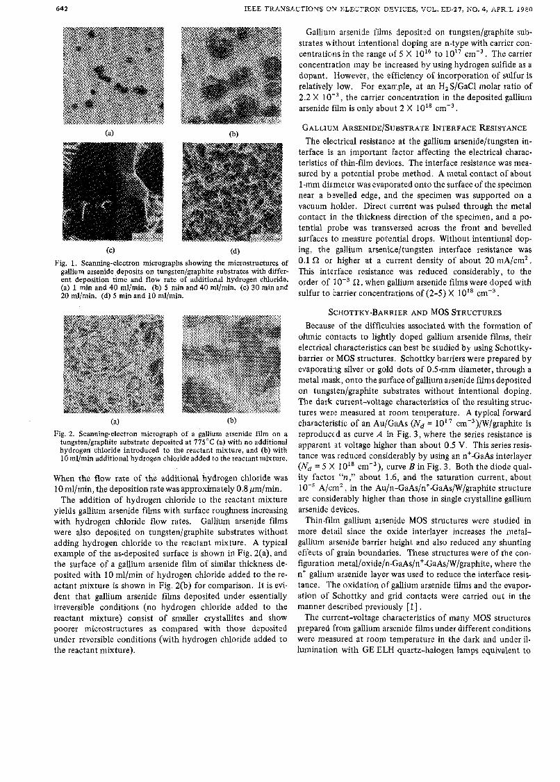
Since the deposition of gallium arsenide, reactions (2a) and (2b), is chemically reversible, the concentration of hydrogen chloride at the substrate surface is a very important factor af- fecting the nucleation and growth of gallium arsenide; the presence of hydrogen chloride tends to reduce the rate of nu- cleation, thus promoting the growth of larger crystallites and affecting the uniformity of the deposited gallium arsenide films. To study this effect, varied amounts of hydrogen chloride (5 to 40 ml/min) were added to the reactant mix.ture near the substrate surface. The effect of hydrogen chloride was most pronounced at high flow rates. Fig. I(a) and (b) shows, re- spectively, the scanning-electron micr0graph.s of the gallium arsenide deposit after 1 and 5 min of deposition with hydro- gen chloride added at a flow rate of 40 ml/min. Although the crystallites are 30-40 pm in size after 5 min o f deposition, only a small fraction of the substrate surface was covered. When the flow rate of the additional hydrogen chloride was re- duced to 20 ml/min, most of the crystallites are up to 100 pm in size after 30 min of deposition, Fig. l(c); however, the gal- lium arsenide film is not continuous. Continuous and uniform films at small thickness were obtained by reducing the flow rate of additional hydrogen chloride. For example, using addi- tional hydrogen chloride at a flow rate of 10 ml/min, the film is continuous after about 5 min of deposition with an average crystallite size of 6-7 pm [Fig, l(d)]. Further reduction in the flow rate of additional hydrogen chloride also reduces the time required to deposit a continuous film and the average size of crystallites; continuous films were found after 3 min of deposition by using a hydrogen chloride flow rate of 5 mllmin.
642 lEEE TRANSACTIONS ON ELECTRON DXYICES, "SOL. ED-27, KO. 4, AFRTL i9$0
Gallium arsenilda films cisposit8::d or1 tungstenlgraphilte sub- strates without intentional doping are n-type with carrier con- centraticlns in the range o f 5 X 10l6 to lo" crnm3. The carrier concentration may be increased by using hydrogen sulfide as a dopant. However, the efficiency of incorporation of sulfur is relatively low. For example, at an H,S/GaCl molar ratio of 2.2 X the carrier concentration in the deposited gallium arsenide film is only about 2 X 1OI8 ~ m - ~ .
GALLIUM ARSENIDE/SlJBSTRATE INTERFACE RESISTANCE \-I
The electrical resistance at the gallium arsenide/tungsten in- terface is; an important factor affecting the electrical charac- teristics of thin-film devices. The interface resistance was mea- sured by a potential probe method. A metal contact of about I-mm dia.meter was evaporated onto the surface of the specimen near a b'svelled edge, and the specimen was supported on a vacuum holder. Direct c.urrent was pulsed through the metal contact in the thickness direction of the specimen, and a po- tential p.robe was transversed across the front and bevelled surfaces to measure pote:ntial drops. Without intentional dop-
(dl ing, the gallium arsenia.e/tungsten interface resistance was Fig. 1. Scanning-electron micrographs showing the microstructures of
gallium arsenide deposits on tungsten/graphite substrates with differ- ent deposition time and flow rate of additional hydrogen chloride. (a) 1 min and 40 ml/min. (b) 5 min and 40 ml/min. (c) 30 min and 20 ml/min. (d) 5 min and 10 ml/min.
(a) (b) Fig. 2. Scanning-electron micrograph of a gallium arsenide film on a
tungsten/graphite substrate deposited at 775°C (a) with no additional hydrogen chloride introduced to the reactant mixture, and (b) with 10 ml/min additional hydrogen chloride added to the reactant mixture.
When the flow rate of the additional hydrogen chloride was 10 ml/min, the deposition rate was approximately 0.8 pm/min.
The addition of hydrogen chloride to the reactant mixture yields gallium arsenide films with surface roughness increasing with hydrogen chloride flow rates. Gallium arsenide films were also deposited on tungsten/graphite substrates without adding hydrogen chloride to the reactant mixture. A typical example of the as-deposited surface is shown in Fig. 2(a), and the surface of a gallium arsenide film of similar thickness de- posited with 10 ml/min of hydrogen chloride added to the re- actant mixture is shown in Fig. 2(b) for comparison. I t is evi- dent that gallium arsenide films deposited under essentially irreversible conditions (no hydrogen chloride added to the reactant mixture) consist of smaller crystallites and show poorer microstructures as compared with those deposited under reversible conditions (with hydrogen chloride added to the reactant mixture).
0.1 B or higher at a cu.rrent density of about 20 mA/cmZ. This interface resistance was reduced considerably, to the order of B, when gallium arsenide films were doped with sulfur to lcarrier concentrations of (2-5) X 10" cm+.
SCHOTTKY-BARRIER AND MOS STRUCTURES
Because of the difficulries associated with the formation of ohmic contacts to lightly doped gallium arsenide films, their electrical characteristics can best be studied by using Schottky- barrier or MOS structures. Schottky barriers were prepared by evaporating silver or gold dots of 0.5-mm diameter, through a metal ma:;k, onto the surface of gallium arsenide films deposited on tungsten/graphite substrates without intentional doping. The dark current-voltage characteristics of the resulting struc- tures wen: measured at room temperature. A typical forward characteristic of an Au/GaAs (Nd = 10' ' ~m-~)/W/graphite is reproduced as curve A in Fig. 3 , where the series resistance is apparent ,at voltage higher than about 0.5 V. This series resis- tance was reduced considerably by using an nt-GaAs interlayer (Nd = 5 X 1OI8 cmT3), curve B in Fig. 3. Both the diode qual- ity factor '%," about 1.6, and the saturation current, about
A/cm2, in the Au/n-GaAs/n+-GaAs/W/graphite structure are considLerably higher than those in single crystalline gallium arsenide devices.
Thin-film gallium arsenide MOS structures were studied in more detail since the oxide interlayer increases the metal- gallium arsenide barrier height and also reduced any shunting effects of grain boundaries. These structures were of the con- figuration metal/oxide/n-GaAs/n+-GaAs/W/graphite, where the n+ galium arsenide layer was used to reduce the interface resis- tance. The oxidation of gallium arsenide films and the evapor- ation of Schottky and grid contacts were carried out in the manner described previously [ I ] .
The current-voltage characteristics of many MOS structures prepared from gallium arsenide films under different conditions were measured at room temperature in the dark and under il- lumination with. GE ELH quartz-halogen lamps equivalent to

CHU et al.: GALLIUM ARSENIDE FILMS FOR SOLAR CELL APPLICATIONS 643
1 L t 10-1 L /
I I I I I I I I I
0.1 0 .2 0 .3 0.4 0.5 0.6 0 .7 0.8 0.9 VOLTAGE. VOLTS
Fig. 3. Dark current-voltage characteristics of Au/nGaAs (Nd = 1017 ~m-~)/W/graphite (curve A ) and Au/n-GaAs (Nd = 10'' ~ m - ~ ) / n+GaAs (Nd = 5 X 10'~ crn-j)/W/graphite (curve B) structures.
10-6 0. 1 0. 2 0. 3 0. 4 0.5
VOLTAGE, VOLTS
Fig. 4. Dark current-voltage characteristics of an Au/oxide/n-GaAs/ n+GaAs/W/graphite structure of 9-cm2 area prepared from gallium arsenide films with no additional hydrogen chloride during deposition.
AM1 conditions. The use of additional hydrogen chloride in the gallium monoch1orid.e-arsenic reactant mixture during the deposition process has been found to have very pronounced ef- fects on the current-voltage characteristics of MOS structures. When gallium arsenide films were deposited without additional hydrogen chloride [Fig. 2(a)] , the MOS structures always ex- hibited excessive dark currents in both forward and reverse di- rections and low rectification ratios, as shown in Fig. 4. This is due presumably to structural discontinuities of grains in the films causing penetration of the contact metal. Because of the excessive dark currents, the conversion efficiency of these structures under illumination is poor, less than 0.5 percent. By introducing additional hydrogen chloride to the gallium monochloride-arsenic mixture, the dark current of MOS struc- tures can be decreased appreciably. Fig. 5 shows typical dark current-voltage Characteristics of an MOS structure prepared from gallium arsenide films with 10 ml/min additional hydrogen chloride during deposition. In this structure, the dark currents are significantly reduced and the rectification ratio increased. However, the saturation current, about A/cm2, is still several orders of magnitude higher than that in single crystal-
0. 1 0.2 0. 3 0.4 0.5 VOLTAGE, VOLTS
Fig. 5. Dark current-voltage characteristics of an Au/oxide/n-GaAs/ n+GaAs/W/graphite structure of 9-cm2 area prepared from gallium arsenide films with 10 ml/min additional hydrogen chloride during deposition.
(a) (b)
Fig. 6. Scanning-electron micrographs of a small region of an MOS structure prepared from a gallium arsenide film with an excessive con- centration of hydrogen chloride in the deposition zone. (a) Secondary electron emission mode. (b) EBIC mode.
line devices, due mainly to carrier recombination at grain boundaries. Under AM1 illumination this type of thin-film gallium arsenide MOS devices have open-circuit voltage, short- circuit current density, and fill factor in the ranges of 0.45- 0.52 V, 11-13.4 mA/cm2, and 55-68 percent, respectively. The relatively high short-circuit current density. indicates that grain boundaries do not seriously degrade the current output. The conversion efficiency of the best cells, without AR coat- ing, is 4.4 percent and would be about 6.7 percent with proper AR coating.
The concentration of hydrogen chloride added to the gallium monochloride-arsenic mixture in the deposition zone is ex- tremely important. The use of an excess hydrogen chloride may have deleterious effects on the photovoltaic characteristics of MOS devices. Since the gallium arsenide film is polycrystal- line and the deposition rate of gallium arsenide is orientation dependent, the resulting film becomes increasingly rough as the concentration of additional hydrogen chloride is increased. The surface roughness could affect the continuity of the thin gold film and reduce the collection efficiency o f light-generated carriers. An example is shown in Fig. 6, where the scanning-

electron micrographs of a small region of an MOS struc:ture prepared from a gallium arsenide film of about 25-pm thick- ness with an excessive concentration of hydrogen chloride in the deposition zone. Fig. 6(a) shows the secondary electron emission micrograph where the grains exhibit good microstruc- ture with well-developed faces. Fig. 6(b) shows the same region photographed in the electron-beam-induced current mode; all grain boundaries as clearly delineated as expected; however, one of the grains shows very low collection efficiency as com- pared with others. This reduced collection is most likely due to the discontinuities in the thin gold film over the :protruded gain.
GaAs,P, - ,/GaAS/W/GRAPHITE STRUCTURES In the thin-film gallium arsenide MOS devices, the short-
circuit current density under AMI conditions is about 80 per- cent of that of single crystalline gallium arsenide solar cells; however, the open-circuit voltage is considerably lower due to the high saturation current in thin-film devices. The open- circuit voltage of an MOS device can be increased by increasing the barrier height in the structure, such as the use of a thin layer of higher energy gap material, gallium phosph:ide or alu- minum arsenide, for example, at the surface of gallium arsenide film. Gallium arsenide forms solid solutions with gallium phosphide over the entire composition range obeying Vegard’s law. The change from a direct to an indirect band. structure occurs at the compositions GaAs,.,,P,., corresponding to an energy gap of 1.9 eV [l 11 .
Thin films of gallium arsenide-phosphide were deposited by the reaction of gallium, hydrogen chloride, arsine, and phos- phine using the same temperature profile and hydrogen chloride flow rate as those used for the deposition of gallium arsenide films. The composition of the solid solution varies with the AsH3/PH3 molar ratios in the reactant mixture; GaAso.8P0.2 and GaAs,.,P,., were obtained by using AsH3/PH3 molar ra- tios of 12 and 6 , respectively. To prepare MOS devices, a gal- lium arsenide-phosphide layer of about l-pm thickness with a graded composition was deposited in-situ following the deposi- tion of gallium arsenide films; the graded composition was used because of the slight difference in lattice parameters of gallium arsenide and gallium arsenide-phosphide. The com- position of the surface region is in the range of GaAs,.,P,., and GaAs,.,P,., . The oxidation and contact formation were carried out in the same manner as described previously. The net carrier concentration in the surface region and the barrier height were determined from capacitance-voltage measure- ments of a silver dot of 0.5-mm diameter at the surface of the device. From the (A/C)’ versus voltage relation, the carrier concentration was calculated to be 2.4 X 10l6 ~ m - ~ , and the barrier height was calculated to be 1.2 eV, about 0.2 eV higher than that in Ag/oxide/n-GaAs structures.
The dark current-voltage characteristics of a Auloxidel GaAs, - ,P,/n-GaAs/n+-GaAsIWlgraphite structure of a 9-cm2 area is shown in Fig. 7. The saturation current in this device is about one order of magnitude lower than that in thin-film gal- lium arsenide MOS devices. Thus its open-circuit voltage under AM1 conditions, 0.63 V, is appreciably higher than that usually obtained from similar gallium arsenide structures, 0.5 V. The
t / CELL AREA. 9 CM2 NO AR COATING
I I l l
0. 1 0. 2 0. 3 0. 4 0. 5 VOLTAGE, VOLTS
Fig. 7. Dark current-voltage characteristics of an AuloxidelGaAsl -xpx/ n-GaAs/n+-GaAs/W/graphite structure.
short-circuit current density and fill factor are 13.3 mA/cm2 and 59.5 percent, respectively, corresponding to an AM1 effi- ciency of 5 .O percent, With proper AR coating, the conversion efficiency would be about 7.5 percent.
SUMMARY AND CONCLUSIONS The reaction between gallium, hydrogen chloride, and arsine
in a hydrogen flow has been used for the deposition of gallium arsenide on tungstenlgraphite substrates for thin-film photo- voltaic devices. The chemical reversibility of this reaction is the most important factor affecting the photovoltaic properties of large-area gallium arsenide films. Films deposited under es- sentially irreversible conditions have poor microstructure and their devices exhibit excessive dark currents resulting in low conversion efficiencies. The introduction of additional hydro- gen chloride to the deposition zone greatly improves the mi- crostructure of gallium arsenide and the photovoltaic charac- teristics of their devices.
The characteristics of MOS devices prepared from n-GaAsI n+-GaAs/W/graphite structures depend strongly on the micro- structure of gallium arsenide films. Using gallium arsenide films prepared with additional hydrogen chloride at the deposi- tion zone, large-area devices with good dark current-voltage characteristics and AM1 efficiencies of 4.4 percent (without AR coating) have been obtained. The open-circuit voltage and the conversion efficiency of these devices can be increased by adding a thin film of gallium arsenide-phosphide at the surface of gallium arsenide.
The gallium arsenide films used in this work are 15-25-pm thickness. It is believed that solar cells with AM1 efficiencies of 10 percent or higher can be produced by further optimizing the process parameters. Additional work must also be directed to cost-reduction approaches such as the use of thinner gallium arsenide films and the simplification of processing steps.
REFERENCES [ I ] S. S. Chu, T. L. Chu, and H. T. Yang, “Thin-film gallium arsenide
solar cells on tungsten/graphite substrates,” Appl . Phys. L e f t . , voi. 32, p . 557,1978.
[2] S. S. Chu, T. L. Chu, H. T. Yang, and K. H. Hong, “Gallium ar- senide films on tungsten/graphite substrates,” J. Electrochem. SOC., vol. 125,p . 1668, 1978.

IEEE TRANSACTIONS ON ELECTRON DEVICES, VOL. ED-21, NO. 4, APRIL 1980 645
[3] S. S. Chu, T. L. Chu, and M. S. Lan, “Gallium arsenide films and
5805,1979. solar cells on graphite substrates,” J. Appl. Phys., vol. 50, p.
[4] P. Rappaport, “Thin film solar cells and a review of recent results on GaAs,”Rev. Phys. Appl., vol. 1, p. 154,1966.
[5] P. D. Dapkus, R. D. Dupuis, R. D. Yingling, J. J. Young, W. I. Simpson, L. A. Modudy, R. E. Johnson, A. G . Campbell, H. M. Manasevit, and R. P. Ruth, “The properties of polycrystalline GaAs materials and devices for terrestrial photovoltaic energy conversion,” in Conf. Rec. 13th IEEE Photovoltaic Specialists Conf., p. 960, June 1978.
[6] Y. C. M. Yeh, F. P. Ernest, and R. J . Stirn, “Progress towards high efficiency polycrystalline thin-film GaAs AMOS solar cells,” in Conf. Rec. 13th IEEE Photovoltaic Specialists Conf., p. 966, June 1978.
[7] K. P. Pande, Y. S. Hsu, J . M. Borrego, and S. K. Ghandhi, “Grain boundary edge passivation of GaAs films by selective anodiza- tion,”Appl. Phys. Lett., vol. 33, p. 117, 1978.
(81 S. W. Ing and H. T. Minden, “Open tube epitaxial synthesis of GaAs and Gap,” J. Electrochem. SOC., vol. 109, p. 995, 1962.
[9] J. R. Knight, D. Effer, and P. R. Evans, ‘The preparation of high purity gallium arsenide by vapor phase epitaxial growth,” Solid- State Electron., vol. 8, p. 178, 1965.
[ 101 M. Rubenstein and E. Myers, “Epitaxial synthesis of GaAs using a flow system,” J. Electrochem. Soc., vol. 113, p. 365, 1966.
[ l l ] J . J . Tietzen and J . A. Amick, “The preparation of properties of vapor-deposited epitaxial GaAs, -xP, using arsine and phos- phine,”J. Electrochem. SOC., vol. 113, p. 724, 1966.
[ 121 P. Rai-Choudhury, “Epitaxial gallium arsenide from trimethyl gallium and arsine,” J. Electrochem SOC., vol. 116, p. 1745, 1969.
[13] V. S. Ban, “Mass spectrometric studies of vapor phase crystal growth,”J. Electrochem. Soc.,vol. 118, p. 1473, 1971.
[ 141 D. W. Shaw, “A comparative thermodynamic analysis of InP and GaAs deposition,” J. Phys. Chem. Solids, vol. 36, p. 111,1975.
The Design and Fabrication of Thin-Film CdS/Cu2S Cells of 9.1 5-Percent Conversion Efficiency
JULIO A. BRAGAGNOLO, ALLEN M. BARNETT, SENIOR MEMBER, IEEE, JAMES E. PHILLIPS, ROBERT B. HALL, ALLEN ROTHWARF, AND JOHN D. MEAKIN
Abstruct-Thin-fiim polycrystalline CdS/Cu2S cells with energy con- version efficiencies in sunlight of up to 9.15 percent and areas of -1 cm2 have been developed. The improvement over previously achieved efficiencies is due to the development of techniques to sepa- rately measure and minimize fill factor losses. Specific design and fabrication changes based on a detailed quantitative analysis of the cell operation, were introduced to correct series resistance, shunt con- ductance and field effect losses. Further increases in efficiency can be expected from the development of a planar junction thin-film CdS/Cu2S cell.
T I. INTRODUCTION
‘HE DIRECT conversion of sunlight to electricity using photovoltaic systems has the potential of providing s ig
nificant amounts of energy from an inexhaustible source by means of a pollution-free process. Requirements of perfor- mance and cost for the active photovoltaic components of flat-plate arrays have been obtained from systems studies [ I ] , [ 2 ] . There is now a measure of agreement, that thin-film polycrystalline solar cells can be developed that will be capa- ble of producing electrical power at a cost competitive with
Manuscript received August 31, 1979; revised October 25, 1979. J . A. Bragagnolo, A. M. Barnett, J . E. Phillips, R. B. Hall, and J. D.
Meakin are with the Institute of Energy Conversion, University of Delaware, Newark, DE 197 11.
A. Rothwarf was with the Institute of Energy Conversion, University of Delaware, Newark. He is now with the Department of Electrical Engineering, Drexel University, Philadelphia, PA.
more conventional techniques and a device based on the CdS/Cu2 S cell is a leading contender fix this achievement.
The importance of demonstrating conversion efficiencies in excess of 10 percent in order to minimize area-related costs, has been underlined by the above studies. Between 1954, when a photovoltaic effect in a junction made by depositing a thin film of copper on a CdS crystal was first reported by Reynolds [3] and 1972, CdS/Cu2S conversion efficiencies in sunlight of between 5-6 percent were reported by many in- vestigators with a limited number of them reporting efficien- cies up to 7 percent [4].
In 1972 a program was initiated at the InsstitUte of Energy Conversion (IEC), University of Delaware, to evaluate the po- tential of the CdS/Cu2S cell as a terrestrial photovoltaic con- verter. Improved control of materials and processes at IEC raised the reproducible conversion efficiency of the type of CdS/Cu2S cell designed by the Clevite Corporation [5] , to close to 7 percent by 1975 [ 6 ] . Improvements of energy con- version efficiencies beyond 7 percent, obtained after 1975 at IEC, were based on the development of the loss minimization method [7]. This method rests on the quantitative analysis of energy losses in a given cell design, both using experimental measurements and theoretical analysis. Information deriving from the loss analysis is utilized to make changes in cell pro- cessing until the achieved efficiency is within 5 percent of the limiting efficiency computed for the cell design under de- velopment. Although some uncertainty exists in the evaluation
0018-9383/80/0400-0645$00.75 0 1980 IEEE