CMOS Differential Amplifier - Wayne State...
29
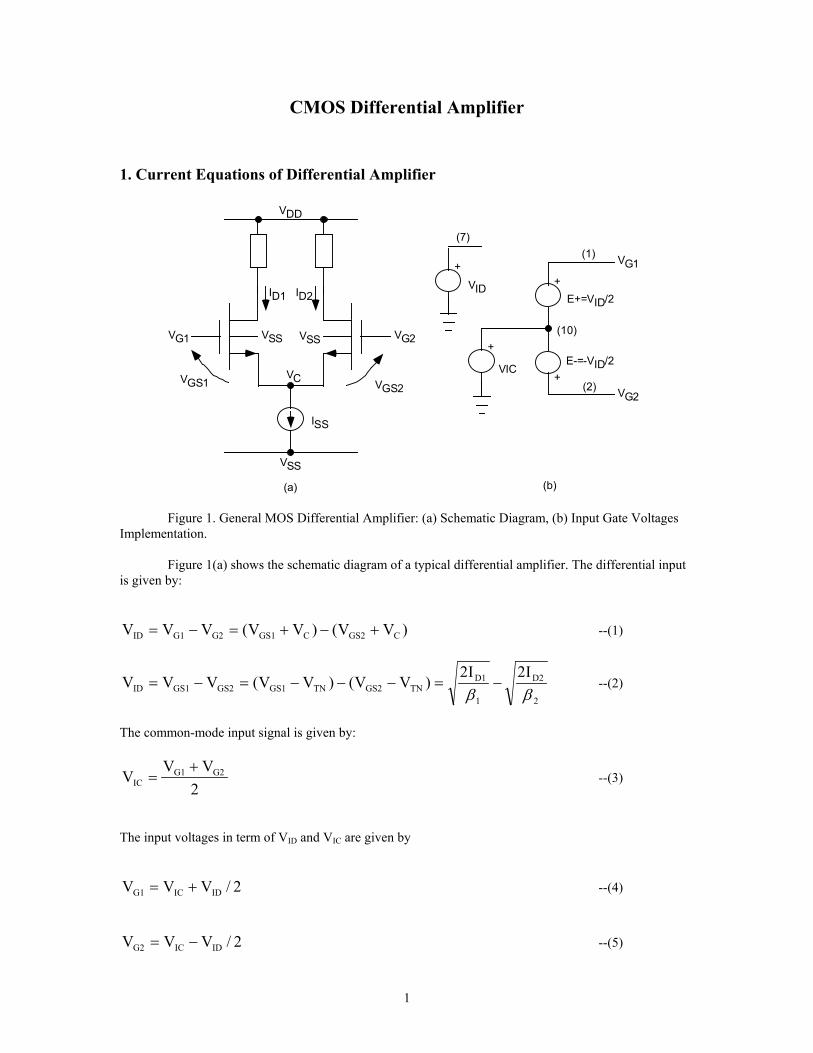
CMOS Differential Amplifier 1. Current Equations of Differential Amplifier V DD V SS V C V SS V SS I SS V G1 V G2 V GS2 V GS1 I D1 I D2 (a) + + + + E+=V ID /2 E-=-V ID /2 (1) (10) (2) V G1 V G2 VIC V ID (7) (b) Figure 1. General MOS Differential Amplifier: (a) Schematic Diagram, (b) Input Gate Voltages Implementation. Figure 1(a) shows the schematic diagram of a typical differential amplifier. The differential input is given by: ) V V ( ) V V ( V V V C GS2 C GS1 G2 G1 ID + − + = − = --(1) 2 D2 1 D1 TN GS2 TN GS1 GS2 GS1 ID I 2 I 2 ) V V ( ) V V ( V V V β β − = − − − = − = --(2) The common-mode input signal is given by: 2 V V V G2 G1 IC + = --(3) The input voltages in term of V ID and V IC are given by 2 / V V V ID IC G1 + = --(4) 2 / V V V ID IC G2 − = --(5) 1
Transcript of CMOS Differential Amplifier - Wayne State...
CMOS Differential Amplifier
1. Current Equations of Differential Amplifier
VDD
VSS
VC
VSS VSS
ISS
VG1 VG2
VGS2VGS1
ID1 ID2
(a)
+
+
+
+
E+=VID/2
E-=-VID/2
(1)
(10)
(2)
VG1
VG2
VIC
VID
(7)
(b) Figure 1. General MOS Differential Amplifier: (a) Schematic Diagram, (b) Input Gate Voltages Implementation.
Figure 1(a) shows the schematic diagram of a typical differential amplifier. The differential input is given by:
)VV()VV(VVV CGS2CGS1G2G1ID +−+=−= --(1)
2
D2
1
D1TNGS2TNGS1GS2GS1ID
I2I2)VV()VV(VVV
ββ−=−−−=−= --(2)
The common-mode input signal is given by:
2VV
V G2G1IC
+= --(3)
The input voltages in term of VID and VIC are given by
2/VVV IDICG1 += --(4)
2/VVV IDICG2 −= --(5)
1

Figure 1(b) shows the implementation of the 2 gate voltages in terms of the differential and common mode voltages. Its PSpice implementation using voltage controlled voltage source is given below: VID 7 0 DC 0V E+ 1 10 7 0 0.5 E- 2 10 7 0 -0.5 VIC 10 0 DC 0V Two special cases of input gate signals are of interests : pure differential and pure common mode input signals. Pure differential input signals mean VIC=0, from equation (4) and (5);
2/VV2/VV
IDG2
IDG1
−==
This case is of interest when studying the differential gain of differential amplifier, see Figure 2(a). Pure common-mode input signals mean VID=0, from equation (4) and (5);
ICG2
ICG1
VVVV
==
This case is of interest when studying the common-mode gain of differential amplifier, see Figure 5(a). Assume both transistor drivers are matched, that is:
βββ == 21
ββD2D1
IDI2I2V −= --(6)
D2D1ID IIV2/ −=β --(7) The transistor currents satisfy the following equations:
D2D1SS III += --(8)
D2D1OD III −= --(9)
2/)II(I ODSSD1 += --(10)
2/)II(I ODSSD2 −= --(11) Substituting Eq(10) and Eq(11) to Eq(7)
2/)II(2/)II(V2/ ODSSODSSID −−+=β --(12)
2

Normalizing by ISS
)II
1II
1(VI SS
OD
SS
ODID
SS
−−+=β
--(13)
To simplify the equation, let
SS
ODID
SS II
=y and , VI
=x β --(14)
The equation reduces to:
y-1y+1=x − Solve for y,
22 y-12-2=y)1(y)1(y)1(2-y)1(x −+−++=
2x1y1
22 −=−
4xx1y1
422 +−=−
)4
x1(xy2
22 −=
The result is:
1|2x| provided ,
4x-1x=y
2
≤ --(15)
Substituting for x and y, one obtains
4IV1V
III
SS
2ID
IDSSSS
OD ββ−= --(16)
2SS
4ID
SS
2ID
SSOD 4IV
IVII ββ
−= --(17)
2SS
4ID
SS
2ID
SSSSD1 4IV
IVI
21I
21I ββ
−+= --(18)
3
2SS
4ID
SS
2ID
SSSSD2 4IV
IVI
21I
21I ββ
−−= , provided β
SSID
I2|V ≤| --(19)
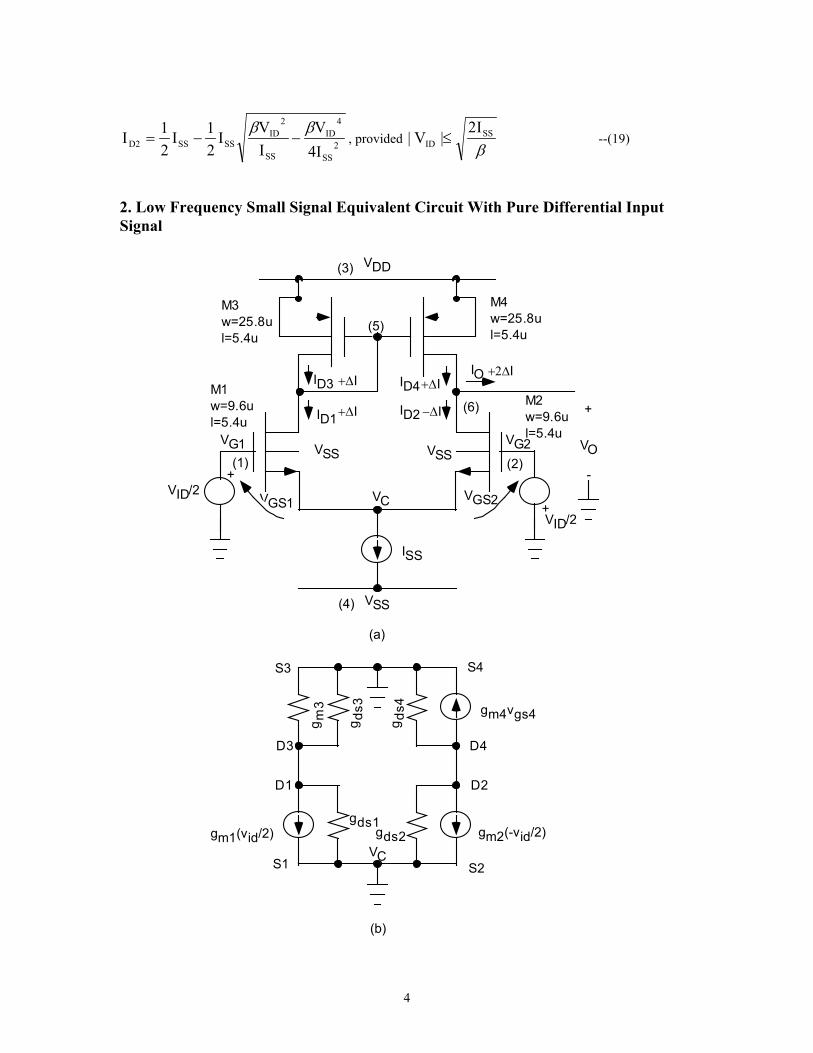
2. Low Frequency Small Signal Equivalent Circuit With Pure Differential Input Signal
VG1
VGS1
VSSVG2
VGS2
VDD
VSS
VC
VSS
ISS
S3
D3
D1
S1
S4
D4
D2
S2
g m3
gds1gds2
gm4vgs4
gm2(-vid/2)gm1(vid/2)
g ds3
g ds4
VC
+
VO
-
ID2
ID4IOID3
ID1
M1w=9.6ul=5.4u
M2w=9.6ul=5.4u
M3w=25.8ul=5.4u
M4w=25.8ul=5.4u
(6)
(3)
(4)
(1) (2)
(5)
(b)
(a)
+VID/2
+VID/2
+2∆I+∆I
+∆I
+∆I
−∆I
4
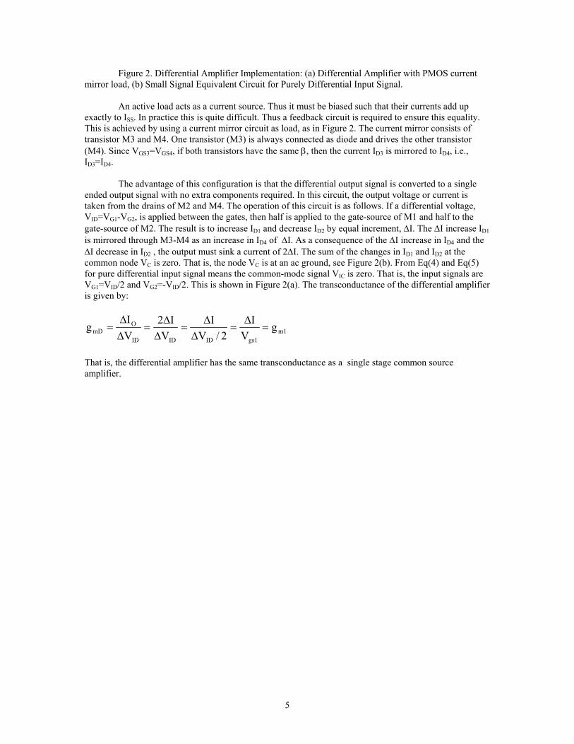
Figure 2. Differential Amplifier Implementation: (a) Differential Amplifier with PMOS current mirror load, (b) Small Signal Equivalent Circuit for Purely Differential Input Signal.
An active load acts as a current source. Thus it must be biased such that their currents add up exactly to ISS. In practice this is quite difficult. Thus a feedback circuit is required to ensure this equality. This is achieved by using a current mirror circuit as load, as in Figure 2. The current mirror consists of transistor M3 and M4. One transistor (M3) is always connected as diode and drives the other transistor (M4). Since VGS3=VGS4, if both transistors have the same β, then the current ID3 is mirrored to ID4, i.e., ID3=ID4. The advantage of this configuration is that the differential output signal is converted to a single ended output signal with no extra components required. In this circuit, the output voltage or current is taken from the drains of M2 and M4. The operation of this circuit is as follows. If a differential voltage, VID=VG1-VG2, is applied between the gates, then half is applied to the gate-source of M1 and half to the gate-source of M2. The result is to increase ID1 and decrease ID2 by equal increment, ∆I. The ∆I increase ID1 is mirrored through M3-M4 as an increase in ID4 of ∆I. As a consequence of the ∆I increase in ID4 and the ∆I decrease in ID2 , the output must sink a current of 2∆I. The sum of the changes in ID1 and ID2 at the common node VC is zero. That is, the node VC is at an ac ground, see Figure 2(b). From Eq(4) and Eq(5) for pure differential input signal means the common-mode signal VIC is zero. That is, the input signals are VG1=VID/2 and VG2=-VID/2. This is shown in Figure 2(a). The transconductance of the differential amplifier is given by:
m1gs1IDIDID
OmD g
VI
2/VI
VI2
VI
g =∆
=∆
∆=
∆∆
=∆∆
=
That is, the differential amplifier has the same transconductance as a single stage common source amplifier.
5
gm2(vid/2) gm4vgs4gds2 gds4
G1 D1
S1 S3
D2
S2
D4
S4
D3=G3=G4
vgs3=vgs4
+
-
+
-
+
-
V2=voV1=vid/2
2gm1(vid/2) gds2 gds4
G1
V1=vid/2
+
-
S1
D2
S2
D4
S4
+
-
V2=vo
gm1vid gds2 gds4
D2
S2
D4
S4
+
-
G1
+
-
S1
V2=voV1=vid
(b)
(c)
g ds3
(a)
g m1(v id/2)
g ds1
g m3
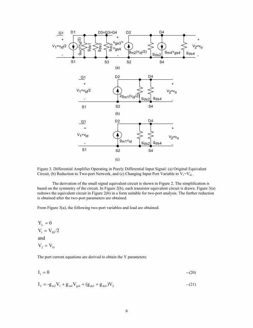
Figure 3. Differential Amplifier Operating in Purely Differential Input Signal: (a) Original Equivalent Circuit, (b) Reduction to Two-port Network, and (c) Changing Input Port Variable to V1=Vid .
The derivation of the small signal equivalent circuit is shown in Figure 2. The simplification is based on the symmetry of the circuit. In Figure 2(b), each transistor equivalent circuit is drawn. Figure 3(a) redraws the equivalent circuit in Figure 2(b) in a form suitable for two-port analysis. The further reduction is obtained after the two-port parameters are obtained. From Figure 3(a), the following two-port variables and load are obtained.
O2
ID1
L
VVand
/2VV0Y
=
==
The port current equations are derived to obtain the Y parameters:
0I1 = --(20)
2ds4ds2gs4m41m22 )Vg(gVgV-gI +++= --(21)
6

Vggg
g-V 1m3ds3ds1
m1gs4 ++
= --(22)
Substitute eq(22) to eq(21)
2ds4ds21m1
2ds4ds21m3ds3ds1
m4m1m2
2ds4ds21m3ds3ds1
m4m11m22
)Vg(gV-2g
)Vg(gV)ggg
gg(g-
)Vg(gVggg
gg-V-gI
++=
++++
+=
++++
=
--(23)
ds3ds1m3m4m3 m2m1 ggg gg gg assuming +>>== The resulting Y-parameter matrix is:
+
=ds4ds2m1 gg2g-
00Y
The dc voltage gain is,
ds4ds2
m1
L22
21
id
O
1
2VD02 gg
g2Yy
y2/V
VVVA
+=
+−===
Instead of half differential input, dc gain with respect to full differential input is desired. That is,
ds4ds2
m2
ds4ds2
m1
id
O
1
2VDO gg
ggg
gVV
VVA
+=
+=== --(24)
7

VG1
VGS1
VSS VG2
VGS2
VDD
VSS
VC
VSS Vo
+
-
M6w=21.6ul=1.2u
M1w=9.6ul=5.4u
M2w=9.6ul=5.4u
M4w=25.8ul=5.4u
M3w=25.8ul=5.4u
M5w=21.6ul=1.2u
ISS=220uA
ID2
ID4IO
ID1
ID3
(1) (2)
(8)
(9)
(4)
(3)
(6)
(5)
IB=220uA
Figure 4. The Complete Differential Amplifier Schematic Diagram Figure 3(c) is the resulting two-port equivalent circuit. Except for the polarity this gain equation is identical to that of the single NMOS inverter with PMOS current load. Figure 4 shows the complete differential amplifier implemented using a pair of inverter amplifier with PMOS current load, and 200uA current souce. The PSpice netlist is given below: * Filename="diffvid.cir" * MOS Diff Amp with Current Mirror Load *DC Transfer Characteristics vs VID VID 7 0 DC 0V AC 1V E+ 1 10 7 0 0.5 E- 2 10 7 0 -0.5 VIC 10 0 DC 0.65V VDD 3 0 DC 2.5VOLT VSS 4 0 DC -2.5VOLT M1 5 1 8 8 NMOS1 W=9.6U L=5.4U M2 6 2 8 8 NMOS1 W=9.6U L=5.4U M3 5 5 3 3 PMOS1 W=25.8U L=5.4U M4 6 5 3 3 PMOS1 W=25.8U L=5.4U M5 8 9 4 4 NMOS1 W=21.6U L=1.2U M6 9 9 4 4 NMOS1 W=21.6U L=1.2U IB 3 9 220UA .MODEL NMOS1 NMOS VTO=1 KP=40U + GAMMA=1.0 LAMBDA=0.02 PHI=0.6 + TOX=0.05U LD=0.5U CJ=5E-4 CJSW=10E-10 + U0=550 MJ=0.5 MJSW=0.5 CGSO=0.4E-9 CGDO=0.4E-9 .MODEL PMOS1 PMOS VTO=-1 KP=15U + GAMMA=0.6 LAMBDA=0.02 PHI=0.6
8
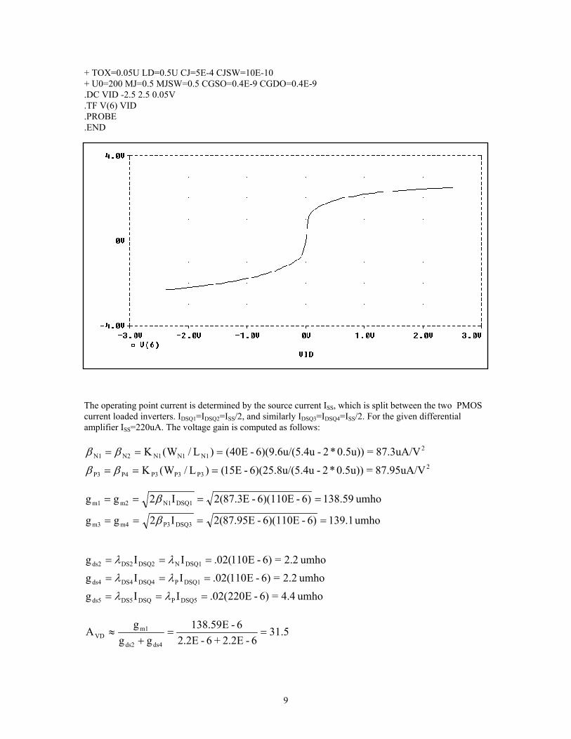
+ TOX=0.05U LD=0.5U CJ=5E-4 CJSW=10E-10 + U0=200 MJ=0.5 MJSW=0.5 CGSO=0.4E-9 CGDO=0.4E-9 .DC VID -2.5 2.5 0.05V .TF V(6) VID .PROBE .END
The operating point current is determined by the source current ISS, which is split between the two PMOS current loaded inverters. IDSQ1=IDSQ2=ISS/2, and similarly IDSQ3=IDSQ4=ISS/2. For the given differential amplifier ISS=220uA. The voltage gain is computed as follows:
87.95uA/V=0.5u))*2-5.4u6)(25.8u/(-E15()L/W(K
87.3uA/V=0.5u))*2-.4u6)(9.6u/(5-E40()L/W(K2
P3P3P3P4P3
2N1N1N1N2N1
===
===
ββ
ββ
umho 1.1396)-6)(110E-E95.87(2I2gg
umho 59.1386)-6)(110E-E3.87(2I2gg
DSQ3P3m4m3
DSQ1N1m2m1
====
====
β
β
umho 4.4=6)-E220(02.IIgumho 2.2=6)-E110(02.IIgumho 2.2=6)-E110(02.IIg
DSQ5PDSQDS5ds5
DSQ1PDSQ4DS4ds4
DSQ1NDSQ2DS2ds2
===
===
===
λλ
λλ
λλ
5.316-2.2E+6-2.2E
6-E59.138gg
gAds4ds2
m1VD ==
+≈
9
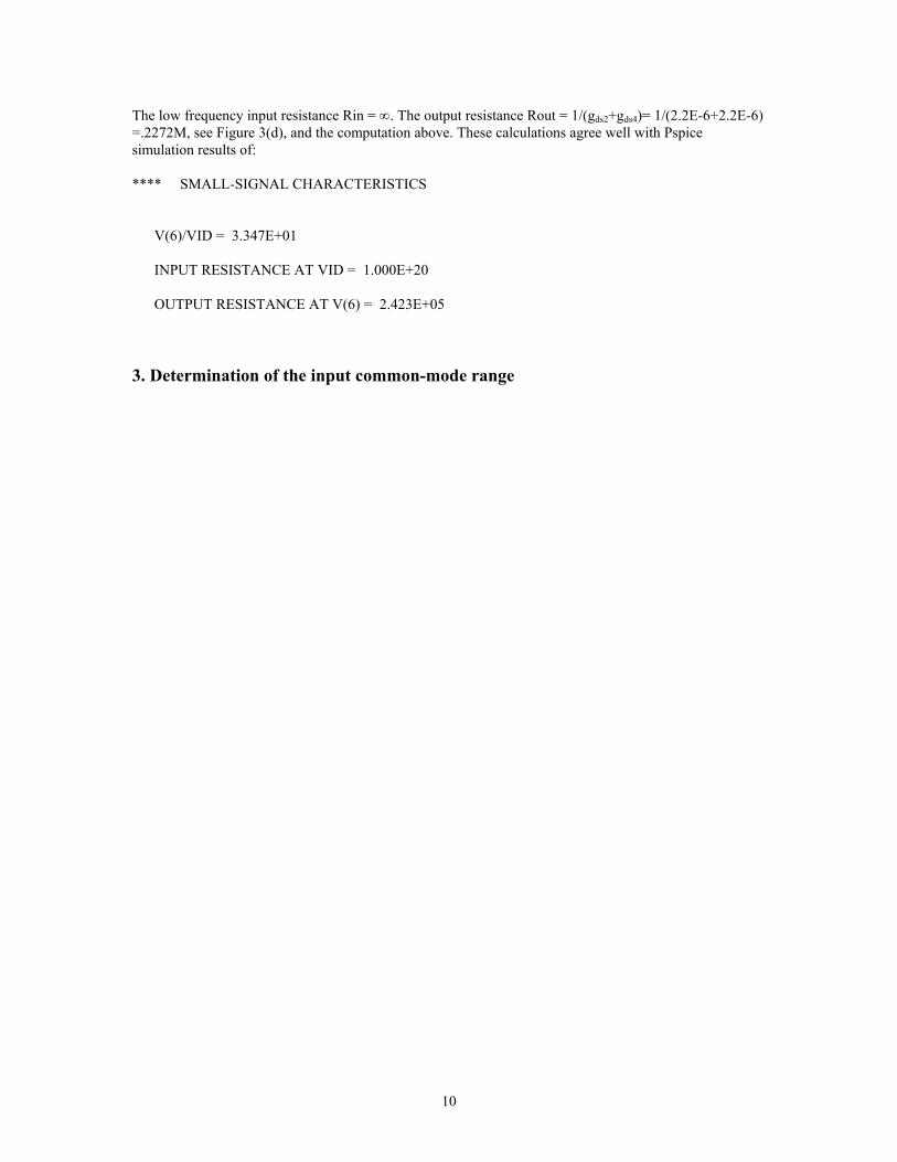
The low frequency input resistance Rin = ∞. The output resistance Rout = 1/(gds2+gds4)= 1/(2.2E-6+2.2E-6) =.2272M, see Figure 3(d), and the computation above. These calculations agree well with Pspice simulation results of: **** SMALL-SIGNAL CHARACTERISTICS V(6)/VID = 3.347E+01 INPUT RESISTANCE AT VID = 1.000E+20 OUTPUT RESISTANCE AT V(6) = 2.423E+05
3. Determination of the input common-mode range
10
VG1
VGS1
VSSVG2
VGS2
VDD
VSS
VC
VSS
ISS
M3 M4
M1 M2
S3
D3
D1
S1
S4
D4
D2
S2
gds1gds2
gm4vgs4
gm2vgs2gm1vgs1
M5VGG
+VIC
+VIC
gds5
Vo
+
-
Vo
+
-
g m3
g ds4
g ds3
VC
VDS5
VDG1
VSD3 VSD4
Vgs3 Vgs4
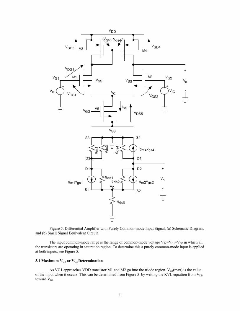
Figure 5. Differential Amplifier with Purely Common-mode Input Signal: (a) Schematic Diagram, and (b) Small Signal Equivalent Circuit. The input common-mode range is the range of common-mode voltage Vic=VG1=VG2 in which all the transistors are operating in saturation region. To determine this a purely common-mode input is applied at both inputs, see Figure 5. 3.1 Maximum VG1 or VG2 Determination As VG1 approaches VDD transistor M1 and M2 go into the triode region. VG1(max) is the value of the input when it occurs. This can be determined from Figure 5 by writing the KVL equation from VDD toward VG1.
11
G=D since ,VVV= VVVV
DG1SG3DD
DG1SD3DDG1
−−−−=
| V||I|2
|V||)V||V(|V TP3P3
DS3TP3TP3GS3SG3 +=+−=
β
DG1TP3P3
DS3DDG1 V|V|
|I|2VV −−−=
β
From Figure 5(a), VDG1 can be determined in term of the commonly known transistor voltages of M1.
DG1GS1DS1
GS1DS1DG1
VVVor
V-VV
+=
=
Transistor M1 is on saturation when the following condition holds.
DG1GS1DS1TN1GS1 VVVVV +=≤− That is,
DG1TN1 VV ≤− The minimum value of VDG1 is achieved when transistor M1 is on the threshold of saturation. That is,
DG1TN1 VV =− The maximum input voltage is obtained when DG1TN1 VV =− . That is,
P3
SSDD
P3
DS3DD
TN1TP3P3
DS3DDG1
IV
|I|2V
V|V||I|2
V(max)V
ββ
β
−=−=
+−−=
--(25)
Assuming |VTP3| ≈VTN1. 3.2 Minimum VG1 or VG2 Determination
12

As VG1 approaches VSS, M1 becomes cutoff. The minimum input voltage VG1 is determined when
M5 is no longer in saturation. This is obtained by writing the KVL equation from VSS to VG1.
GS1DS5SSG1 VVVV ++= Transistor M5 is on saturation when,
DS5TN5GS5 VVV ≤−
M5 is at verge of saturation when, DS5(SAT)DS5TN5GS5 VVVV ==−
That is, the minimum input voltage occurs when, DS5(SAT)TN5GS5 VVV =− .
GS1DS5(SAT)SSG1 VVV(min)V ++= --(26)
GS1TN5GS5SSG1 V)V(VV(min)V +−+=
N1
SSGG
N1
DS1GG
TN1N1
DS1TN5GG
TN1TN1GS1TN5SSGGSSG1
IV
2IV
V2I
VV
V)V-V()VVV(V(min)V
ββ
β
+=+=
++−=
++−−+=
--(27)
Ignoring the bulk bias effect. Using the SPICE parameters for the differential amplifier implemented in Figure 4. From Eq(25),
P3
SSDDG1
IV(max)V
β−=
233PP3 uA/V 87.95=0.5u))*2-5.4u6)(25.8u/(-E15()L/W(K ==β
V 92.058.15.26-87.95E
6-E2205.2(max)VG1 =−=−=
and from Eq(27),
V 38.02.158.12.187.3
6-E220VI
(min)V GGN1
SSG1 =−=−=+=
β
To guarantee that the differential amplifier stays on the linear region of operation, set common-mode signal at half way the common-mode range. That is, VIC=[VG1(max)+VG1(min)]/2=[0.92+.38]/2=0.65.
4. Low Frequency Small Signal Equivalent Circuit With Pure Common-Mode Input Signal
13
2gm1vgs1
D1
S1
D3
S3
+
-
G1
+
-
V2=voV1=Vic
gds5
g ds1+gds2
g ds3+gds4+g m3+g m4
Vgs1
D5
S5
VC
YL
(c)
gm1vgs1gm2vgs2 gds2 gds4
G1 D1
S1
S3
D2
S2
D4
S4
D3=G3=G4+
-
vo
+
-
vgs1
+
-
gds5
+
-
Vic Vc
vgs3
g ds1
D5
g m4vgs4
S5
+
-
vgs4
g ds3+gm3
g ds4+gm4
gm1vgs1gm2vgs2 gds2
G1 D1
S1
S3
D2
S2
D4
S4
D3=G3=G4+
-
vo
+
-
vgs1
+
-
gds5
+
-
Vic Vc
vgs3
g ds1
g ds3+gm3
D5
S5
(b)
(a)
I2
I2
Figure 6. Small Signal Equivalent Circuit: (a) Original Small Signal Equivalent Circuit, (b) Accounting for Source Values and Polarities, and (c) Two-port Conversions.
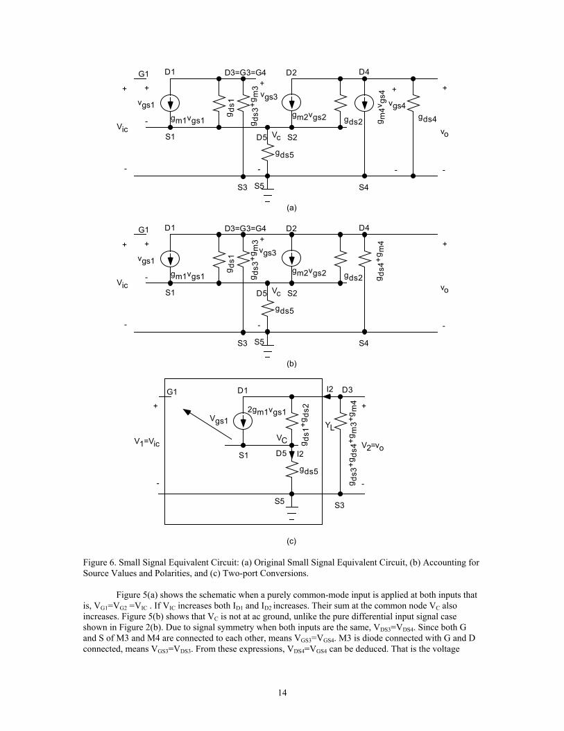
Figure 5(a) shows the schematic when a purely common-mode input is applied at both inputs that is, VG1=VG2 =VIC . If VIC increases both ID1 and ID2 increases. Their sum at the common node VC also increases. Figure 5(b) shows that VC is not at ac ground, unlike the pure differential input signal case shown in Figure 2(b). Due to signal symmetry when both inputs are the same, VDS3=VDS4. Since both G and S of M3 and M4 are connected to each other, means VGS3=VGS4. M3 is diode connected with G and D connected, means VGS3=VDS3. From these expressions, VDS4=VGS4 can be deduced. That is the voltage
14

across D and S of M4 can be labelled as VGS4, see Figure 6(a). The current source of M4 is therefore reduced to conductance gm4, see Figure 6(b). Since VDS3=VDS4, the D3 and D4 can be connected together. Figure 6(c) shows the final equivalent circuit after combining all components that are in parallel.
From Figure 6(c), the following two-port variables and load are obtained.
O2
IC1
m3ds4ds3
m3ds3m4m3ds4ds3L
VVand
VVgg gg assuming
g2g2ggggY
=
===
+=+++=
m4
The two-port current equations are derived to obtain the Y parameters.
2m1ds5ds2ds1
ds5ds2ds11
m1ds5ds2ds1
ds5m12
2ds5
m1ds2ds12ds2ds11m12
2ds5
C
Cm1ds2ds12ds2ds11m1
C1m1C2ds2ds12
1
V2gggg
)ggg(V
2gggggg2
I
Ig
1)2gg(g-)Vg(gV2gI
Ig
1V
)V2gg(g-)Vg(gV2g )V-(V2g)V-)(Vg(gI
0I
++++
++++
=
++++=
=
++++=++=
=
The Y-parameter matrix is:
m4m3ds2ds1
m1ds5ds1
ds5ds1
m1ds5ds1
ds5m1
m1ds5ds2ds1
ds5ds2ds1
m1ds5ds2ds1
ds5m1
gg gg assuming2gg2g
gg22gg2g
gg200
2gggg)ggg(
2gggggg2
00Y
==
++++=
++++
+++=
The dc common-mode voltage gain is,
15
.gg assuming
rg21
rg2gg
rg21gg
g2g2g
1gg
gg
)2gg2g)(gg(2gg2gg2
)gg(22gg2g
gg22gg2g
gg2
YyyA
ds3m3
ds5m3ds5m1
m3
m1
ds5m1
m3
m1
ds5
m1ds1
m3
ds1
m3
m1
m1ds5ds1m3ds3ds5ds1
ds5m1
m3ds3m1ds5ds1
ds5ds1
m1ds5ds1
ds5m1
L22
21VC0
>>
−≈
−≈
+
−≈
+++
−=
++++−
=
++++
++−
=+
−=
* Filename="diffvic.cir" * MOS Diff Amp with Current Mirror Load *DC Transfer Characteristics vs VIC VID 7 0 DC 0V E+ 1 10 7 0 0.5 E- 2 10 7 0 -0.5 VIC 10 0 DC 0V VDD 3 0 DC 2.5VOLT VSS 4 0 DC -2.5VOLT M1 5 1 8 8 NMOS1 W=9.6U L=5.4U M2 6 2 8 8 NMOS1 W=9.6U L=5.4U M3 5 5 3 3 PMOS1 W=25.8U L=5.4U M4 6 5 3 3 PMOS1 W=25.8U L=5.4U M5 8 9 4 4 NMOS1 W=21.6U L=1.2U M6 9 9 4 4 NMOS1 W=100.8U L=3.6U M7 9 9 3 3 PMOS1 W=3.6U L=3.6U .MODEL NMOS1 NMOS VTO=1 KP=40U + GAMMA=1.0 LAMBDA=0.02 PHI=0.6 + TOX=0.05U LD=0.5U CJ=5E-4 CJSW=10E-10 + U0=550 MJ=0.5 MJSW=0.5 CGSO=0.4E-9 CGDO=0.4E-9 .MODEL PMOS1 PMOS VTO=-1 KP=15U + GAMMA=0.6 LAMBDA=0.02 PHI=0.6 + TOX=0.05U LD=0.5U CJ=5E-4 CJSW=10E-10 + U0=200 MJ=0.5 MJSW=0.5 CGSO=0.4E-9 CGDO=0.4E-9 .OP .DC VIC -2.5 2.5 0.05V .TF V(6) VIC .PROBE .END
16

01582.0)6)(.2272E6-E1.139(2
1rg2
1Ads5m3
VCO −=−=−=
This is very closed to the PSpice simulation result. **** SMALL-SIGNAL CHARACTERISTICS
17

V(6)/VIC = -1.459E-02 INPUT RESISTANCE AT VIC = 1.000E+20 OUTPUT RESISTANCE AT V(6) = 2.386E+05 The goal of differential amplifier is to amplify the difference signal and to reject common-mode signal. A figure of merit called common-mode rejection ration (CMRR) is defined as:
15.19910.01582-
5.31AA
CMRRVC
VD ===
5. Differential Gain Frequency Response
18
VG1 +
VGS1
VSSVG2+
VGS2
VDD
VSS
VC
VSS
ISS
M3 M4
M1 M2
CLCgd2
Cdb4
Cdb2
Cgs4Cgs3
Cgd4
Cdb3
Cgd1
(a)
Cdb1
VGS1
VSS
VGS2
VSS
VC
VSS
ISS
M3 M4
M1 M2
C2
C3
C1
(b)
VDD
VG2+
VG1 +
C1=Cgd1+Cdb1+Cdb3+Cgs3+Cgs4C2=Cgd2+Cdb2+Cdb4+CLC3=Cgd4
(1) (2)
(5) (6)
(8)
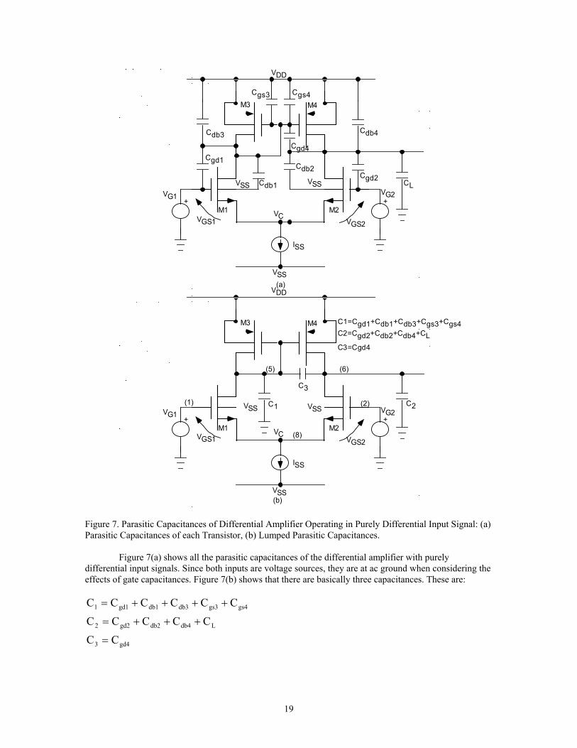
Figure 7. Parasitic Capacitances of Differential Amplifier Operating in Purely Differential Input Signal: (a) Parasitic Capacitances of each Transistor, (b) Lumped Parasitic Capacitances. Figure 7(a) shows all the parasitic capacitances of the differential amplifier with purely differential input signals. Since both inputs are voltage sources, they are at ac ground when considering the effects of gate capacitances. Figure 7(b) shows that there are basically three capacitances. These are:
gd43
Ldb4db2gd22
gs4gs3db3db1gd11
CCCCCCC
CCCCCC
=
+++=
++++=
19

gm1(vid/2)
g ds1+gds3+g m3
C1
C3
gm2(vid/2) gm4vgs4 g ds2+gds4
C2
G1 D1
S1
D3=G3=G4
S3
D2 D4
S2 S4
+
vo
-
+
vid/2
-
gm1(vid/2) gm1(vid/2) gm4vgs4
G1 D1
S1
D3=G3=G4
S3
D2 D4
S2 S4
+
-
+
-
I3 +
-
Vgs4
C1=Cgd1+Cdb1+Cdb3+Cgs3+Cgs4C2=Cgd2+Cdb2+Cdb4+CLC3=Cgd4
(a)
(b)
Y3
Y1 Y2V1=Vid/2 V2=VO
=
gm1=gm2
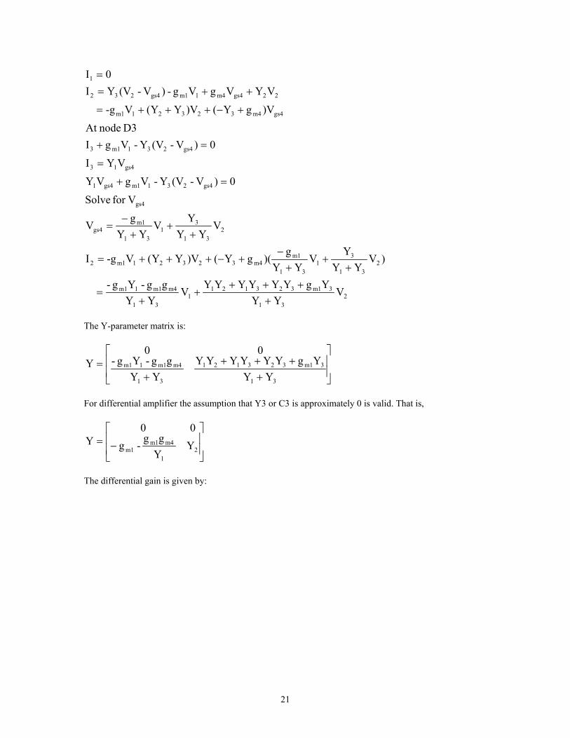
Figure 8. High Frequency Small Signal Equivalent Circuit: (a) Small Signal Equivalent Circuit Showing Lumped Capacitances, (b) Small Signal Equivalent Circuit Combining Capacitance and Resistance to Admittance. NOTE C3 is not a miller capacitance, it is connected between the outputs of the two inverter amplifiers, and not between an output and an input terminals of an amplifier. C3 in this case is normally small and can be ignored. Figure 8(b) shows that the three admittances are given by:
gd433
2ds4ds22
1m3ds3ds11
CCYCggY
CgggY
sss
s
==++=
+++=
The two-port Y parameters are to be determined. Figure 8(b) shows that the two-port variables are:
O2
id1
L
VVand
2/VV0Y
=
==
20
231
3m13231211
31
m4m11m1
231
31
31
m1m432321m12
231
31
31
m1gs4
gs4
gs4231m1gs41
gs413
gs4231m13
gs4m432321m1
22gs4m41m1gs4232
1
VYY
YgYYYYYYV
YYgg-Yg-
)VYY
YV
YYg)(gY()VYY(V-gI
VYY
YV
YYgV
Vfor Solve
0)V-(VY-VgVY
VYI
0)V-(VY-VgID3 nodeAt
)VgY()VYY(V-g
VYVgVg-)V-(VYI0I
++++
++
=
++
+−
+−+++=
++
+−
=
=+
=
=+
+−+++=
++==
The Y-parameter matrix is:
++++
+=
31
3m1323121
31
m4m11m1
YYYgYYYYYY
YYgg-Yg-
00Y
For differential amplifier the assumption that Y3 or C3 is approximately 0 is valid. That is,
−=
21
m4m1m1 Y
Ygg-g
00Y
The differential gain is given by:
21
+
+
++
+
+++
+
+
=
+
+
++
+++
+++
++++
+
=
+++++++++
=++
++++
=
+=
+=
+−
==
ds4ds2
2
m3ds3ds1
1
m4m3ds3ds1
1
ds4ds2
m1
ds4ds2
2
m3ds3ds1
1m3ds3ds1
m4m3ds3ds1
1m4m3ds3ds1
ds4ds2
m1
2ds4ds21m3ds3ds1
1m4m3ds3ds1m1
2ds4ds2
1m3ds3ds1
m4m1
2
1
m4m1
2
1
m4m1m1
L22
21
1
2VD2
ggC1
gggC1
ggggC1
ggg2
ggC1
gggC1)ggg(
ggggC1)gggg(
ggg
)Cg)(gCgg(g)Cggg(gg
)Cg(g
)Cggg
g(1g
Y
)Yg(1g
YYggg
Yyy
VVA
ss
s
ss
s
sss
ss
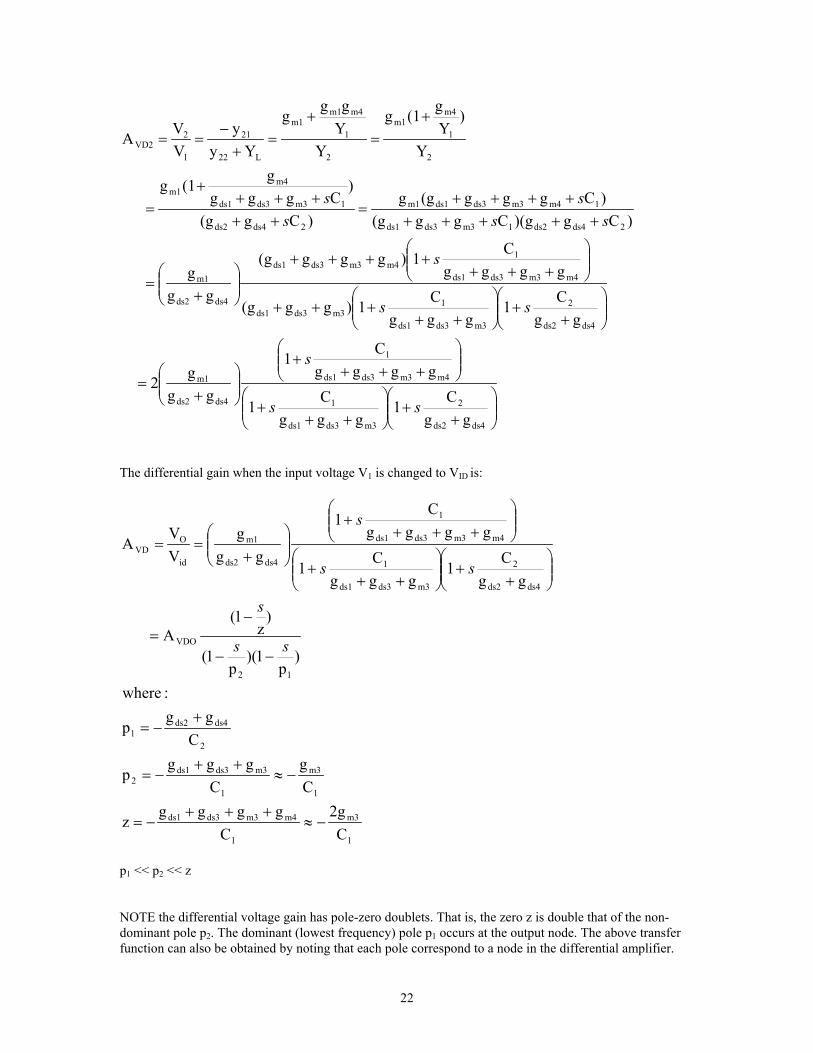
The differential gain when the input voltage V1 is changed to VID is:
1
m3
1
m4m3ds3ds1
1
m3
1
m3ds3ds12
2
ds4ds21
12
VDO
ds4ds2
2
m3ds3ds1
1
m4m3ds3ds1
1
ds4ds2
m1
id
OVD
C2g
Cgggg
z
Cg
Cggg
p
Cgg
p
:where
)p
1)(p
1(
)z
1(A
ggC1
gggC1
ggggC
1
ggg
VV
A
−≈+++
−=
−≈++
−=
+−=
−−
−=
+
+
++
+
+++
+
+
==
ss
s
ss
s
p1 << p2 << z NOTE the differential voltage gain has pole-zero doublets. That is, the zero z is double that of the non-dominant pole p2. The dominant (lowest frequency) pole p1 occurs at the output node. The above transfer function can also be obtained by noting that each pole correspond to a node in the differential amplifier.
22

Each node is at a finite impedance with respect to ground. That is, each node there is a resistance Rn (or conductance) and capacitance Cn to ground. To determine which poles are dominant (or more significant), the impedance levels must be monitored. The parasitic capacitances Cn are of approximately the same magnitude, but Rn usually vary considerably. When the resistance (conductance) is high (low), a dominant pole is generated. The impedance levels are summarized in the follwing table: Node(From Netlist) Resistance Capacitance Pole 1 0 (ac ground) X 2 0 (ac ground) X 5 R5=1/(gds1+gds3+gm3) C1 p2=1/(R5C1)* 6 R6=1/(gds2+gds4) C2 p1=1/(R6C2) 8 0 (ac ground) X The derivation shows that the pole p2 create a zero doublet. * Filename="diffreq.cir" * MOS Diff Amp with Current Mirror Load *DC Transfer Characteristics vs VID VID 7 0 DC 0V AC 1V E+ 1 10 7 0 0.5 E- 2 10 7 0 -0.5 VIC 10 0 DC 0.65V VDD 3 0 DC 2.5VOLT VSS 4 0 DC -2.5VOLT M1 5 1 8 8 NMOS1 W=9.6U L=5.4U M2 6 2 8 8 NMOS1 W=9.6U L=5.4U M3 5 5 3 3 PMOS1 W=25.8U L=5.4U M4 6 5 3 3 PMOS1 W=25.8U L=5.4U M5 8 9 4 4 NMOS1 W=21.6U L=1.2U M6 9 9 4 4 NMOS1 W=100.8U L=3.6U M7 9 9 3 3 PMOS1 W=3.6U L=3.6U .MODEL NMOS1 NMOS VTO=1 KP=40U + GAMMA=1.0 LAMBDA=0.02 PHI=0.6 + TOX=0.05U LD=0.5U CJ=5E-4 CJSW=10E-10 + U0=550 MJ=0.5 MJSW=0.5 CGSO=0.4E-9 CGDO=0.4E-9 .MODEL PMOS1 PMOS VTO=-1 KP=15U + GAMMA=0.6 LAMBDA=0.02 PHI=0.6 + TOX=0.05U LD=0.5U CJ=5E-4 CJSW=10E-10 + U0=200 MJ=0.5 MJSW=0.5 CGSO=0.4E-9 CGDO=0.4E-9 .AC DEC 100 1HZ 100000GHZ .PROBE .END
23

6. Common-Mode Frequency Response
24

VG1
VGS1
VSS VG2
VGS2
VDD
VSS
VC
VSS
M3 M4
M1 M2
M5VGG
+VIC
+VIC
Vo
+
-
Cdb5
Csb2Csb1
Cgd5
VG1
VGS1
VSS VG2
VGS2
VDD
VSS
VC
VSS
M3 M4
M1 M2
M5VGG
+VIC
+VIC
Vo
+
-
CS
CS=Csb1+Csb2+Cdb5+Cgd5
Figure 9. Differential Amplifier Operating in Pure Common-Mode Input Signal: (a) All Parasitic Capacitances at Common Node Vc, (b) Total Capacitances Across the Drain and Source of M5.
From the expression of the dc common-mode gain, it is primarily a function of gm3 and rds5. The first order frequency response analysis can be simplified by ignoring all parasitic capacitances except the capacitance CS across rds5, see Figure 9. That is rds5 is replaced by zds5 in the the common-mode gain expression to account for frequency dependency.
25

gd5db5sb2sb1S
ds5m3
Sds5
Sds5
ds5m3
ds5m3VC
Sds5
ds5Sds5ds5
CCCCC:where
rg2)Cr1(
Cr1r
g2
1zg21A
Cr1r
)//Cr(z
+++=
+−=
+
−=
−=
+==
s
s
s
* Filename="diffreqc.cir" * MOS Diff Amp with Current Mirror Load *DC Transfer Characteristics vs VIC VID 7 0 DC 0V E+ 1 10 7 0 0.5 E- 2 10 7 0 -0.5 VIC 10 0 DC 0.65V AC 1V VDD 3 0 DC 2.5VOLT VSS 4 0 DC -2.5VOLT M1 5 1 8 8 NMOS1 W=9.6U L=5.4U M2 6 2 8 8 NMOS1 W=9.6U L=5.4U M3 5 5 3 3 PMOS1 W=25.8U L=5.4U M4 6 5 3 3 PMOS1 W=25.8U L=5.4U M5 8 9 4 4 NMOS1 W=21.6U L=1.2U M6 9 9 4 4 NMOS1 W=100.8U L=3.6U M7 9 9 3 3 PMOS1 W=3.6U L=3.6U .MODEL NMOS1 NMOS VTO=1 KP=40U + GAMMA=1.0 LAMBDA=0.02 PHI=0.6 + TOX=0.05U LD=0.5U CJ=5E-4 CJSW=10E-10 + U0=550 MJ=0.5 MJSW=0.5 CGSO=0.4E-9 CGDO=0.4E-9 .MODEL PMOS1 PMOS VTO=-1 KP=15U + GAMMA=0.6 LAMBDA=0.02 PHI=0.6 + TOX=0.05U LD=0.5U CJ=5E-4 CJSW=10E-10 + U0=200 MJ=0.5 MJSW=0.5 CGSO=0.4E-9 CGDO=0.4E-9 .AC DEC 100 1HZ 100000GHZ .PROBE .END
26

The differential-mode voltage gain decreases with increasing frequency but common-mode voltage increases. Therefore, CMRR decreases with increasing frequency.
7. Designing Differential Amplifier With Specified CMR Given a common-mode range of –0.75 <= VIC <=0.75 , VGG=-1, ISS=IDS5=100uA, Lmin=5.4u,
. Determine the size of each transistor in the differential amplifier circuit, see Figure 4.
5.0VVV TNGS =−=∆
1. Determine the (W/L)5 to sink 100uA.
===
==
==
u4.5u10820
1]-(-2.5)-6)[-1-(40E6)-E100(2
)V-V-V(KI2
)V-V(KI2
LW
)V-V(LW
2K
)V-V(2
I
2
2TN5SSGGN
DS52
TN5GS5N
DS5
5
2TN5GS5
5
N2TN5GS5
N5DS5
β
2. Determine (W/L)1 =(W/L)2 from VIC(min)=VG1(min) specification From Eq(26),
27

====
=
=−−−−=−−−≥
−≥++==
u4.5u21640
1)-6)(1.25-E40(6)-E50(2
)V-(VKI2
LW
LW
25.15.0)5.2(75.0VV75.0V
75.0VVVmin)(VV
22TNGS1N
DS1
21
DS5(SAT)SSGS1
GS1DS5(SAT)SSG1IC
3. Determine (W/L)3=(W/L)4 from VIC(max)=VG1(max) specification From Eq(25),
====
==
−==
u4.5u75.11177.2
0.75)-6)(2.5-E15(6)-E50(2
(max))V-(VK|I|2
LW
(max))V-V(LW
2K
(max))V-V(2
|I|
|I|2V(max)V(max)V
22G1DDP
DS3
3
2G1DD
3
P2G1DD
P3DS3
P3
DS3DDG1IC
β
β
The above is simulated using PSpice. The results agree well with the calculations.
* Filename="diffcmr.cir" * MOS Diff Amp with Current Mirror Load *DC Transfer Characteristics vs VIC VID 7 0 DC 0V E+ 1 10 7 0 0.5 E- 2 10 7 0 -0.5 VIC 10 0 DC 0V VDD 3 0 DC 2.5VOLT VSS 4 0 DC -2.5VOLT M1 5 1 8 8 NMOS1 W=216U L=5.4U M2 6 2 8 8 NMOS1 W=216U L=5.4U M3 5 5 3 3 PMOS1 W=11.75U L=5.4U M4 6 5 3 3 PMOS1 W=11.75U L=5.4U M5 8 9 4 4 NMOS1 W=108U L=5.4U VGG 9 0 DC -1V .MODEL NMOS1 NMOS VTO=1 KP=40U + GAMMA=1.0 LAMBDA=0.02 PHI=0.6 + TOX=0.05U LD=0.5U CJ=5E-4 CJSW=10E-10 + U0=550 MJ=0.5 MJSW=0.5 CGSO=0.4E-9 CGDO=0.4E-9 .MODEL PMOS1 PMOS VTO=-1 KP=15U + GAMMA=0.6 LAMBDA=0.02 PHI=0.6 + TOX=0.05U LD=0.5U CJ=5E-4 CJSW=10E-10 + U0=200 MJ=0.5 MJSW=0.5 CGSO=0.4E-9 CGDO=0.4E-9 .DC VIC -2.5 2.5 0.05V .TF V(6) VIC .PROBE .END
28
29