Chapter 8 FPGA Basics - SOC & DSP Labsocdsp.ee.nchu.edu.tw/class/download/vlsi_dsp_102/ni… ·...
28
YT Hwang VLSI DSP 1 Chapter 8 FPGA Basics NCHU EE Yin-Tsung Hwang YT Hwang VLSI DSP 2 What are PLDs?
Transcript of Chapter 8 FPGA Basics - SOC & DSP Labsocdsp.ee.nchu.edu.tw/class/download/vlsi_dsp_102/ni… ·...

YT Hwang VLSI DSP 1
Chapter 8 FPGA Basics
NCHU EEYin-Tsung Hwang
YT Hwang VLSI DSP 2
What are PLDs?

YT Hwang VLSI DSP 3
Programmable Logic Devices
• A pre-fabricated ASIC capable of performing any logic subject to user programming
• compromise between the semi-custom ASICs and standard components
• a collection of logic elements placed in a programmable interconnection framework
• fast design turn around time
• field programmable EPROM, E2PROM, Flash, SRAM based
YT Hwang VLSI DSP 4
PLD Programmability (1)
• programmable combinational logic PT-based, LUT
LUT(look-up
table)
PT-based building block• 2-level logic, high fan-in
LUT-based building block• 4-5 inputs, fine-grain arch.• ROM like

YT Hwang VLSI DSP 5
PLD Programmability (2)
• programmable register register type, register control
YT Hwang VLSI DSP 6
PLD Programmability (3)
• programmable interconnect routing resources including switching elements,
local/global lines, clock buffers

YT Hwang VLSI DSP 7
PLD Programmability (4)
• programmable I/O direction, I/O register, 3-state, slew rate
YT Hwang VLSI DSP 8
Field Programmability
• can verify designs at any time by configuring the FPGA/ CPLD devices on board via the download cable or hardware programmer

YT Hwang VLSI DSP 9
PLD Classifications
• General classification Simple programmable logic device (SPLD) Complex programmable logic device (CPLD) Field programmable gate array (FPGA)
• Classification by programming technology Fuse, anti-fuse (OTP) EPROM, EEPROM, Flash (multiple programming) SRAM (volatile, need configuration when power up)
• Classification by routing structures Segmented (incremental) routing Continuous routing
YT Hwang VLSI DSP 10
Simple PLD
• Programmable AND/OR array Sum-Of-Product (SOP) to implement Boolean
functions
• facilitated with FFs, output macros, and feedback path
• foldback architecture
• low density, low cost, fixed delay
• examples: PAL, GAL, PEEL, FPLA

YT Hwang VLSI DSP 11
PAL Architecture
YT Hwang VLSI DSP 12
Complex PLD architecture

YT Hwang VLSI DSP 13
Field Programmable Gate Array
• architecture originates from gate array• 2-D array of programmable logic blocks (cells)• programmable / incremental interconnect• less predictable timing, place &routing is
crucial• matrix based architecture
Xilinx XC4000, Spartan, Virtex, QuickLogic
• Row based architecture Actel ACT families
• Continuous interconnect architecture Altera Flex 8K/10K, APEX
YT Hwang VLSI DSP 14
Generic FPGA logic cell
Carrylogic
Look-UpTable(RAM)
Macro-cell
I/Ocells
Mcell
PrimaryInputs
Logic cell
16X1

YT Hwang VLSI DSP 15
Continuous v.s. Segmented
CROSSBAR
continuous segmented
YT Hwang VLSI DSP 16
Rapid Prototyping & System Verification
• To see is to believe
• The ASIC respin cost is too high
• Verification at lower speed

YT Hwang VLSI DSP 17
Low cost solution of FPGAs
• Hardcopy technology Reduced die area
Only two mask layer cost
YT Hwang VLSI DSP 18
Latest FPGA Features
• Advanced process For example, Xilinx Spartan III use 90nm process
Next generation Virtex FPGA will contain 1G transistors in 70nm process
• High logic gate count Up to millions of logic gates
• Large on chip memory From several K bits to several M bits
• On chip processor ARM 7/9, PowerPC
• On chip multiplier/DSP
• High speed I/O Up to 3.125Gbps

YT Hwang VLSI DSP 19
What’s inside?
• Altera Excalibur Processor +
Memory +
1,000,000 plus
logic capacity
PLD Area for Customer Design
ARM922TCore
Single-PortRAM
Dual-PortRAM
YT Hwang VLSI DSP 20
SoPC example
EBI Bridge
SRAM(Single Port)
SDRAMController
DPRAM
SDRAM Interface
FlashInterface
ARMProcessorP
LL
s
Stripe
33-MHz Utopia-2
PHYManager
CustomLogic
AMBABus
Inter-face
Master Port
Slave Port
Dual-Port RAM Interface
Logic
Ethernet Controller
MediaIndependentInterface
AMBABus
Inter-face
AMBABus
Inter-face
ATM Cell ProcessorNios
CPU
PCIController
PCIAMBABus
Inter-face
Bridge

YT Hwang VLSI DSP 21
FPGA Architecture Overview
YT Hwang VLSI DSP 22
Memory ResourcesSRL16 registersDistributed MemoryBlock MemoryExternal Memory
System ClockManagementDigital Delay Lock Loops (DLLs)
I/O ConnectivitySelectIOTM TechnologySupport major I/O standards
Logic & RoutingFlexible logic implementationVector Based RoutingInternal 3-State bussing
The Spartan-IIE SolutionMore Than Just Silicon
. . .
. . .
. . .
. . .
IOB
IOB
IOB
IOB
CLB CLB RAM
RAM
RAM
RAM
IOBIOB DLLDLL
CLB CLB
DLL IOB IOB DLL

YT Hwang VLSI DSP 23
F5IN
CINCLKCE
COUT
D Q
CK
S
REC
D Q
CK
REC
OG4G3G2G1
Look-UpTable
Carry&
ControlLogic
O
YBY
F4F3F2F1
XBX
Look-UpTable
BYSR
S
Carry&
ControlLogic
SLICE
COUT
D Q
CK
S
REC
D Q
CK
REC
OG4G3G2G1
Look-UpTable
Carry&
ControlLogic
O
YBY
F4F3F2F1
XBX
Look-UpTable
F5INBYSR
S
Carry&
ControlLogic
CINCLKCE SLICE
CLB Structure
• Each slice has 2 LUT-FF pairs with associated carry logic
• Two 3-state buffers (BUFT) associated with each CLB, accessible by all CLB outputs
CLB Slice Structure
• Each slice contains two sets of the following: Four-input LUT
Any 4-input logic function Or 16-bit x 1 sync RAM Or 16-bit shift register
Carry & Control Fast arithmetic logic Multiplier logic Multiplexer logic
Storage element Latch or flip-flop Set and reset True or inverted inputs Sync. or async. control

YT Hwang VLSI DSP 26
CLB
MUXF6
Slice
LUT
LUTMUXF5
Slice
LUT
LUTMUXF5
Dedicated Expansion Multiplexers
• MUXF5 combines 2 LUTs to create 4x1 multiplexer Or any 5-input function (LUT5) Or selected functions up to 9 inputs
• MUXF6 combines 2 slices to form 8x1 multiplexer Or any 6-input function (LUT6) Or selected functions up to 19 inputs
• Dedicated muxes are faster and more space efficient

YT Hwang VLSI DSP 27
RAM16X1S
O
DWE
WCLKA0A1A2A3
RAM32X1S
O
DWEWCLKA0A1A2A3A4
RAM16X2S
O1
D0
WEWCLKA0A1A2A3
D1
O0
=
=LUT
LUT or
LUT
RAM16X1D
SPO
D
WE
WCLK
A0
A1
A2
A3
DPRA0 DPO
DPRA1
DPRA2
DPRA3
or
Distributed RAM
• CLB LUT configurable as Distributed RAM A LUT equals 16x1 RAM
Implements Single and Dual-Ports
Cascade LUTs to increase RAM size
• Synchronous write
• Synchronous/Asynchronous read Accompanying flip-flops used
for synchronous read
YT Hwang VLSI DSP 28
D QCE
D QCE
D QCE
D QCE
LUT
INCE
CLK
DEPTH[3:0]
OUTLUT =
Shift Register
• Each LUT can be configured as shift register Serial in, serial out
• Dynamically addressable delay up to 16 cycles
• For programmable pipeline
• Cascade for greater cycle delays
• Use CLB flip-flops to add depth

YT Hwang VLSI DSP 29
Shift Register
• Register-rich FPGA Allows for addition of pipeline stages to increase throughput
• Data paths must be balanced to keep desired functionality
64Operation A
4 Cycles 8 Cycles
Operation B
3 Cycles
Operation C64
12 Cycles
3 Cycles9-Cycle imbalance
YT Hwang VLSI DSP 30
12 Cycles
64Operation A
4 Cycles 8 Cycles
Operation B
3 Cycles
Operation C
12 Cycles Paths staticallybalanced
9 Cycles
Pipeline
64
Shift Register
• LUT as shift register Used to add pipeline stages
• Increase overall register count 16 bit shift register per LUT 64 bit shift register per CLB

YT Hwang VLSI DSP 31
CLB Arithmetic Logic
• Dedicated carry logic Provides high performance for
counters & arithmetic functions
Discrete XOR component for single level sum completion
Two separate carry chains in CLB allow for 3 operand functions
Can also be used to cascade LUTs for wide-input logic functions
Single-level Sum
LUT
01
LUT
01
LUT
01
LUT
01
YT Hwang VLSI DSP 32
COUT
Look-UpTable
SLICE0CIN
COUT
O
Look-UpTable
Carry&
ControlLogic
Look-UpTable
SLICE1CIN
CLB
Look-UpTable
B1B0
A1A0
C1C0
SUM1
SUM0
PARTIAL0
PARTIAL1Carry
&ControlLogic
Carry&
ControlLogic
Carry&
ControlLogic
3 Operand Adder Function
• A, B, C are two-bits wide SUM = A + B + C or PARTIAL + C, where PARTIAL = A + B Implementation
First 2-operand sum ‘A+B’ is performed in Slice 0 Second 2-operand sum ‘PARTIAL + C’ is performed in Slice 1
Fast local feedback connection within the CLB Very small delay for on PARTIAL

YT Hwang VLSI DSP 33
Carry Logic forWide Input Functions
• Higher performance
• Efficient resource utilization
• Common applications Wide input decoding
Comparators
• HDL design entry LUT can be inferred
MUXCY must be instantiated
YT Hwang VLSI DSP 34
12- Input AND Function
• Utilization 3 LUTs and 3 MUXCYs As opposed to 4 LUTs
• Performance 1 logic level As opposed to 2 logic levels
0 1
INIT=8000
0 1
INIT=8000
0 1
INIT=8000
Output
Vcc
LUT1
LUT2
LUT3
DCBA
HGFE
LKJI
MUXCY
MUXCY
MUXCY
4-Input AND Truth TableInputs(ABCD) Output(Z) Output(HEX)
0000 00001 00010 00011 0…… .. ..1011 0 ..1100 01101 01110 01111 1
0
8

YT Hwang VLSI DSP 35
12- Input OR Function
0 1
INIT=0001
0 1
INIT=0001
0 1
INIT=0001
Vcc
Vcc
Vcc
Output
LUT1
LUT2
LUT3
DCBA
HGFE
LKJI
MUXCY
MUXCY
MUXCY
4-Input NOR Truth TableInputs(ABCD) Output(Z) Output(HEX)
0000 10001 00010 00011 0…… .. ..1011 0 ..1100 01101 01110 01111 0
1
0
• Utilization 3 LUTs and 3 MUXCYs As opposed to 4 LUTs
• Performance 1 logic level As opposed to 2 logic levels
YT Hwang VLSI DSP 36
CO
DI CIS
LUT
CY_MUX
CY_XOR
MULT_AND
A
B
A x B
Dedicated AND gate
Dedicated CLB Multiplier Logic
• Dedicated AND gate• Highly efficient ‘Shift & Add’ implementation
For a 16x16 Multiplier 30% reduction in area and one less logic level

YT Hwang VLSI DSP 37
DSP Coefficients Small FIFOs Scratch Pad
16x1
Distributed RAM• Single-port• Dual port• Cascadable
Cache Tag memory Large FIFOs Packet buffers Video line buffers
Block RAMs• 4Kbit blocks• True dual-port
SDRAMSGRAM
PB SRAMDDR SRAMZBT SRAMQDR SRAM
High-Performance External Memory Interfaces•DDR I/O•SSTL, HSTL, CTT
Spartan-IIE Memory Hierarchy
DCLK
A3A2A1A0
QSRL16D
CLK
A3A2A1A0
QSRL16ECE
Shift Register LUT• 16 registers, 1 LUT• Compact & fast
Pipelining Buffers
Block RAM
4Kx12Kx21Kx4512x8256x16
Port A
Port B
Collaboration with memory vendors
IDT, Cypress, Micron, NEC, Samsung, Toshiba...
BytesKilobytes
YT Hwang VLSI DSP 38
RAM16X1S
O
DWE
WCLKA0A1A2A3
RAM32X1S
O
DWEWCLKA0A1A2A3A4
RAM16X2S
O1
D0
WEWCLKA0A1A2A3
D1
O0
=
=LUT
LUT or
LUT
RAM16X1D
SPO
D
WE
WCLK
A0
A1
A2
A3
DPRA0 DPO
DPRA1
DPRA2
DPRA3
or
Distributed RAM
• CLB LUT configurable as Distributed RAM A LUT equals 16x1 RAM Implements single and
dual ports Cascade LUTs to
increase RAM size
• Synchronous write• Synchronous/Asynchronous read
Accompanying flip-flops used for synchronous read

YT Hwang VLSI DSP 39
SRL-16 and SRL-16E
DCLK
A3A2A1A0
QSRL16
16-bit Shift Register Look-Up-Table
D
CLK
A3A2A1A0
QSRL16ECE
16-bit Shift Register Look-Up-Table with Clock Enable
D QCE
D QCE
D QCE
D QCE
LUT
INCE
CLK
ADDR[3:0]
OUT
Slice
LUT
LUT
Slice
LUT
LUT
CLB
YT Hwang VLSI DSP 40
DPA[3:0]
A[3:0]WEDWCLK
DPO
SPO
RAM16X1D
16 x 1RAM
16 x 1RAM
Distributed RAMDual-Port Implementation
• 2 LUTs equal 16x1 dual-port RAM
• A Port Uses A[3:0] address
Write and read
• B Port Uses DPA[3:0] address
Read only
• Excellent for FIFOs, scratch pads….

YT Hwang VLSI DSP 41
Block RAM
Spartan-IIETrue Dual-Port
Block RAM
Port A
Port B
Block RAM
• Most efficient memory implementation Dedicated blocks of memory
• Ideal for most memory requirements 8 to 72 memory blocks
4096 bits per blocks
Use multiple blocks for larger memories
• Builds both single and true dual-port RAMs• CORE Generator provides custom-sized block
RAMs Quickly generates optimized RAM implementation
YT Hwang VLSI DSP 42
Device No. of Blocks Block RAM BitsXC2S50E 8 32,768XC2S100E 10 40,960XC2S150E 12 49,152XC2S200E 14 57,344XC2S300E 16 65,536XC2S400E 40 163,840XC2S600E 72 294,912
Block RAM
• Configurable synchronous Block RAM Single-port RAM
True dual-port RAM
Two independent single-port RAMs
• Block count increases with FPGA size

YT Hwang VLSI DSP 43
Block RAM
• Flexible 4096-bit block… Variable aspect ratio 4096 x 1
2048 x 2
1024 x 4
512 x 8
256 x 16
• Increase memory depth or width by cascading blocks
YT Hwang VLSI DSP 44
RAMB4_S4
RAMB4_S4
DO[3:0]
WE
EN
RST
ADDR[9:0]
CLK
DI[3:0]DATA[7..4]
DATA[3..0]
OUT[7..4]
OUT[3..0]
1024 X 8 RAM
DO[3:0]
WE
EN
RST
ADDR[9:0]
CLK
DI[3:0]
Block RAMSingle-Port Implementation
• Easy cascading of block RAMs• Utilize variable aspect ratio for
desired RAM size• Example
Desired RAM size: 1024 x 8 1024 x 4 + 1024 x 4 = 1024 x 8
• CORE Generator software Efficiently cascades
RAM blocks Quick custom
RAM implementation

YT Hwang VLSI DSP 45
RAMB4_S4_S16
Port A Out4-Bit Width
Port B In256-Bit Depth
Port A In1K-Bit Depth
Port B Out16-Bit Width
DOA[3:0]
DOB[15:0]
WEA
ENA
RSTA
ADDRA[9:0]
CLKA
DIA[3:0]
WEB
ENB
RSTB
ADDRB[7:0]
CLKB
DIB[15:0]
Dual-Port Bus Flexibility
• Each port can be configured with a different data bus width
• Provides easy data width conversion without any additional logic
YT Hwang VLSI DSP 46
VCC, ADDR[10:0]
GND, ADDR[10:0]
RAMB4_S1_S1
Port B Out1-Bit Width
DOA[0]
DOB[0]
WEA
ENA
RSTA
ADDRA[10:0]
CLKA
DIA[0]
WEB
ENB
RSTB
ADDRB[10:0]
CLKB
DIB[0]
Port B In2K-Bit Depth
Port A Out1-Bit Width
Port A In2K-Bit Depth
Two Independent Single-Port RAMs
• To access the lower RAM Tie the MSB address bit to Logic
Low• To access the upper RAM
Tie the MSB address bit to Logic High
• Added advantage of True Dual-Port No wasted RAM Bits
• Can split a Dual-Port 4K RAM into two Single-Port 2K RAM Simultaneous independent
access to each RAM

YT Hwang VLSI DSP 47
• Content Addressable Memory (CAM) Storage array like a RAM
Functionally opposite of a RAM Quickly find the location of a particular stored value
Output the address and toggle the MATCH line, if data match is found
• Used in telecommunications, networking, Ethernet, ATM switches
• Xilinx provides reference designs and application notes
1024x8ADD[9:0] DATA [7:0]
RAM
1024x8DATA[7:0] ADD [9:0]
CAM
MATCH
CAM in Block RAM
YT Hwang VLSI DSP 48
w Supports multiple voltage and signal standards simultaneously
w Eliminate costly bus transceivers
System Interfaces -- SelectI/O™
Voltage Standards2.5V 1.8V3.3V 1.5V
SSTLHSTLCTT
High-speed Memory Interfaces
Chip-to-Chip Interfaces
LVTTLLVCMOSLVPECLLVDS
Backplane Interfaces
GTL GTL+AGP PCI BLVDS
19 DifferentStandardsSupported!

YT Hwang VLSI DSP 49
SelectI/OTM Standards
• VCCO defines output voltage
Standard VREF VCCO
Chip to Chip InterfaceLVTTL na 3.3LVCMOS2 na 2.5LVCMOS18 na 1.8LVDS na 2.5LVPECL na 3.3
Backplane InterfacePCI 33MHz 3.3V na 3.3PCI 66MHz 3.3V na 3.3GTL 0.80 naGTL+ 1.00 naAGP-2X 1.32 3.3Bus LVDS na 2.5
Memory InterfaceHSTL-I 0.75 1.5HSTL-III & IV 0.90 1.5SSTL3-I & II 1.50 3.3SSTL2-I & II 1.25 2.5CTT 1.50 3.3
User I/O Pin
VCCO
VREF
InternalReference
Output
Input
• VREF defines input threshold reference voltage• Available as user I/O when using internal
reference
YT Hwang VLSI DSP 50
I/Os Separated into 8 Banks
Bank 3
IOB=I/O Blocks
Bank 2
Bank 1Bank 0
Bank 4Bank 5
Bank 6
Bank 7 . . .
. . .
. . .
. . .
IOB
IOB
IOB
IOB
CLB CLBRAM
RAM
RAM
RAM
IOBIOB DLLDLL
CLB CLB
DLL IOB IOB DLL
GCLK0GCLK1
GCLK2GCLK3
Ban
ks 2
and
3 u
sed
durin
g co
nfig
urat
ion

YT Hwang VLSI DSP 51
I/O Signal Types
LVCMOS HSTL SSTL
Single-Ended
LVDS Bus LVDS LVPECL
Differential
I/O Signal Type
LVTTL
NOTE: Only the popular IO types shown here
YT Hwang VLSI DSP 52
Data Out
Driver Receiver
Data In
LVTTL input levels
1.2V swing
Logic High
Logic Low0.8 V
2 V
3.3 V
Single ended data transfer
Single Ended I/O
• Traditional means of data transfer
• Data is carried on a single line
• Bigger voltage swing between logic Low and High
YT Hwang VLSI DSP 53
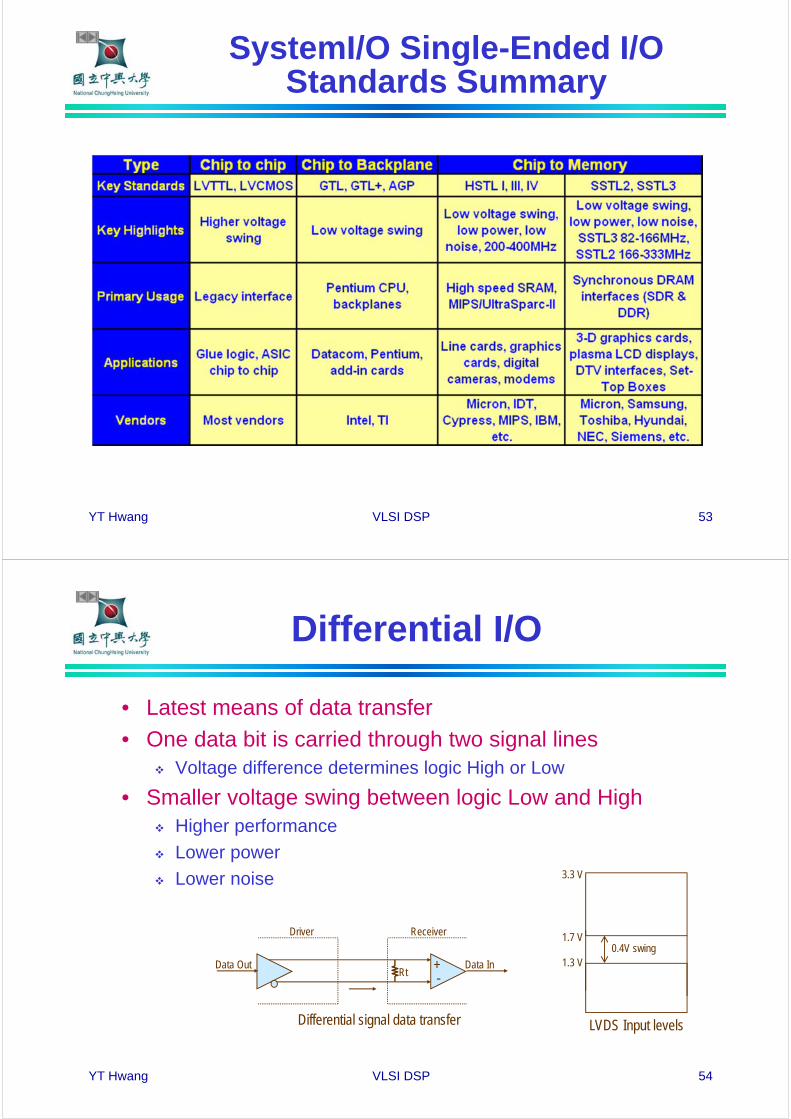
SystemI/O Single-Ended I/O Standards Summary
YT Hwang VLSI DSP 54
Data OutRt
Driver Receiver
Data In-+
LVDS Input levels
0.4V swing1.3 V
1.7 V
3.3 V
Differential signal data transfer
Differential I/O
• Latest means of data transfer
• One data bit is carried through two signal lines Voltage difference determines logic High or Low
• Smaller voltage swing between logic Low and High Higher performance
Lower power
Lower noise

YT Hwang VLSI DSP 55
SelectI/O: Differential I/O Types
• LVDS (Low Voltage Differential Signal) Unidirectional data transfer
• Bus LVDS Bi-directional communication between 2 or more devices
Can transmit and receive LVDS signals through the same pins
• LVPECL (Low Voltage Positive Emitter Coupled Logic) Unidirectional data transfer
Popular industry standard for fast clocking