Atomic-resolution imaging of lattice imperfections in ... Magazine, Vol. 86, Nos. 29–31, 11...
18
Philosophical Magazine, Vol. 86, Nos. 29–31, 11 Oct.–1 Nov. 2006, 4589–4606 Atomic-resolution imaging of lattice imperfections in semiconductors by combined aberration-corrected HRTEM and exit-plane wavefunction retrieval K. TILLMANN*, L. HOUBEN and A. THUST Ernst Ruska–Centre for Microscopy and Spectroscopy with Electrons and Institute of Solid State Research, Research Centre Ju¨lich, D-52425 Ju¨lich, Germany (Received 23 November 2005; in final form 5 March 2006) With improvements in the instrumental information limit and the simultaneous minimization of image delocalization, high-resolution transmission electron microscopy is presently enjoying increased popularity for the atomic-scale imaging of lattice imperfections in solid-state materials. In this study, the benefits of a combination of spherical aberration-corrected imaging and numerical retrieval of the exit-plane wavefunction from a focal series of micrographs are illustrated by highlighting their combined use for atomic-scale characterization of lattice defects frequently observed in common semiconductor materials. Thus, experimental analyses will review the core structure of Lomer dislocations at In 0.3 Ga 0.7 As/GaAs heterointerfaces and focus on atomic lattice displacements associated with extrinsic stacking faults in GaAs, as well as on the core structure of chromium implantation-induced Frank partial dislocations in GaN at directly interpretable contrast features. Supplementary, practical advantages of the retrieval of the exit-plane wavefunction for the subsequent numerical elimination of residual lens aberrations are demonstrated. 1. Introduction Over the past 50 years, transmission electron microscopy has become the technique of choice whenever structural properties associated with lattice imperfections in solid-state materials have been investigated experimentally. Even though enormous progress has been made in the characterization of dislocations, stacking faults and internal boundaries in common semiconductor materials, there is still much to learn about the precise atomic configuration in the vicinity of these structural imperfections. The task is also of technological interest as further developments in applied semiconductor research need a greater understanding of the interaction between structural and electronic properties with advancing miniaturization [1, 2]. In other words, the detailed evaluation of electronic features induced by lattice *Corresponding author. Email: [email protected] Philosophical Magazine ISSN 1478–6435 print/ISSN 1478–6443 online ß 2006 Taylor & Francis http://www.tandf.co.uk/journals DOI: 10.1080/14786430600675763
-
Upload
nguyennhan -
Category
Documents
-
view
217 -
download
1
Transcript of Atomic-resolution imaging of lattice imperfections in ... Magazine, Vol. 86, Nos. 29–31, 11...
Philosophical Magazine,Vol. 86, Nos. 29–31, 11 Oct.–1 Nov. 2006, 4589–4606
Atomic-resolution imaging of lattice imperfections insemiconductors by combined aberration-corrected HRTEM
and exit-plane wavefunction retrieval
K. TILLMANN*, L. HOUBEN and A. THUST
Ernst Ruska–Centre for Microscopy and Spectroscopy with Electronsand Institute of Solid State Research,
Research Centre Julich, D-52425 Julich, Germany
(Received 23 November 2005; in final form 5 March 2006)
With improvements in the instrumental information limit and the simultaneousminimization of image delocalization, high-resolution transmission electronmicroscopy is presently enjoying increased popularity for the atomic-scaleimaging of lattice imperfections in solid-state materials. In this study, the benefitsof a combination of spherical aberration-corrected imaging and numericalretrieval of the exit-plane wavefunction from a focal series of micrographs areillustrated by highlighting their combined use for atomic-scale characterization oflattice defects frequently observed in common semiconductor materials. Thus,experimental analyses will review the core structure of Lomer dislocations atIn0.3Ga0.7As/GaAs heterointerfaces and focus on atomic lattice displacementsassociated with extrinsic stacking faults in GaAs, as well as on the core structureof chromium implantation-induced Frank partial dislocations in GaN at directlyinterpretable contrast features. Supplementary, practical advantages of theretrieval of the exit-plane wavefunction for the subsequent numerical eliminationof residual lens aberrations are demonstrated.
1. Introduction
Over the past 50 years, transmission electron microscopy has become the technique
of choice whenever structural properties associated with lattice imperfections in
solid-state materials have been investigated experimentally. Even though enormous
progress has been made in the characterization of dislocations, stacking faults and
internal boundaries in common semiconductor materials, there is still much to learn
about the precise atomic configuration in the vicinity of these structural
imperfections. The task is also of technological interest as further developments in
applied semiconductor research need a greater understanding of the interaction
between structural and electronic properties with advancing miniaturization [1, 2].
In other words, the detailed evaluation of electronic features induced by lattice
*Corresponding author. Email: [email protected]
Philosophical Magazine
ISSN 1478–6435 print/ISSN 1478–6443 online � 2006 Taylor & Francis
http://www.tandf.co.uk/journals
DOI: 10.1080/14786430600675763
imperfections and the elucidation of the atomic structure of these imperfections are
interdependent [3, 4].Recent fields of interest in high-resolution transmission electron microscopy
(HRTEM) include (i) the pursuit of sub-Angstrom resolution at medium accelerationvoltages [5–7] in association with (ii) the direct interpretability of micrographs [8–10]
characterized by (iii) a rather low image delocalization in the vicinity of latticeimperfections [11, 12]. To realize these objectives simultaneously, two sophisticated
techniques, not available with ‘traditional’ medium voltage instruments equippedwith field emission gun emitters, have attracted much recent interest.
The first, double hexapole corrector elements, enabling compensation fordetrimental lens aberrations, are in practical use [13, 14]. As a result, the aberration
coefficient CS emerges an additional parameter for extending the point resolutionin phase-contrast imaging to the information limit together with simultaneous
maximization of phase contrast and minimization of contrast delocalization [15].Moreover, with a negative CS value combined with a specific overfocus settingZopt>0, a substantial contrast improvement is not only achieved but low-nuclear
charge elements can also be imaged at bright atom contrasts in the vicinity ofhigh-nuclear charge atoms [8, 9].
The other, numerical technique enables restoration of the phase �(r) and
amplitude A(r) of the exit-plane wavefunction from a focal series [16–18] or anillumination tilt direction series [19, 20] of experimental micrographs. Thus, all spatialinformation up to (focal series) or beyond (tilt direction series) the axial information
limit of the instrument can be retrieved, allowing also for subsequent eliminationof residual lens aberrations still present in aberration-corrected microscopy [21–24].
The objective of this contribution is to demonstrate the advantage of combining
these techniques for the atomic scale imaging of structural imperfections insemiconductor materials. Special emphasis is placed on the conceptual advantages
for lattice defect characterization at atomic resolution and the quantification ofatomic column positions in the vicinity of lattice imperfections in semiconductormaterials.
2. Methodical background: Negative spherical aberration-corrected imaging
in tandem with numerical retrieval of exit-plane wavefunction
In aberration-corrected microscopy, a high amount of negative phase-contrast maybe obtained simultaneously with widely minimized image delocalization, when
setting the constant of spherical aberration to an optimized value [9, 15]
CS ¼ �64=27��3g�4max ð1Þ
and choosing an overfocus setting of the objective lens
Zopt ¼ 16=9��1g�2max ð2Þ
with � and 1/gmax denoting the electron wavelength and the information limit ofthe instrument, respectively. A corresponding instrument set-up yields directly
4590 K. Tillmann et al.
interpretable high-resolution micrographs accompanied by residual imagedelocalization of
R ¼ 16=27 g�1max ð3Þ
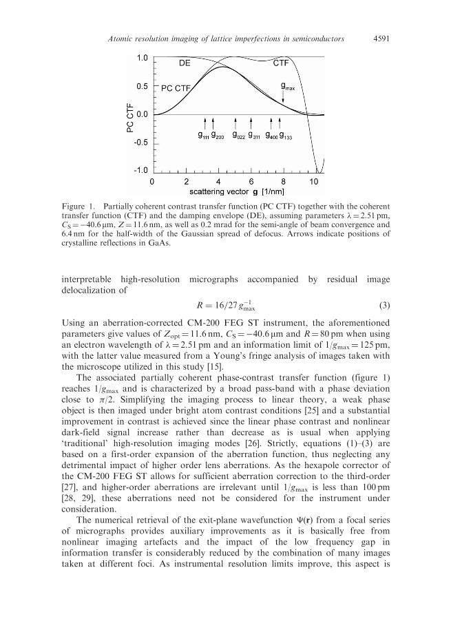
Using an aberration-corrected CM-200 FEG ST instrument, the aforementionedparameters give values of Zopt¼ 11.6 nm, CS¼�40.6mm and R¼ 80 pm when usingan electron wavelength of �¼ 2.51 pm and an information limit of 1/gmax¼ 125 pm,with the latter value measured from a Young’s fringe analysis of images taken withthe microscope utilized in this study [15].
The associated partially coherent phase-contrast transfer function (figure 1)reaches 1/gmax and is characterized by a broad pass-band with a phase deviationclose to �/2. Simplifying the imaging process to linear theory, a weak phaseobject is then imaged under bright atom contrast conditions [25] and a substantialimprovement in contrast is achieved since the linear phase contrast and nonlineardark-field signal increase rather than decrease as is usual when applying‘traditional’ high-resolution imaging modes [26]. Strictly, equations (1)–(3) arebased on a first-order expansion of the aberration function, thus neglecting anydetrimental impact of higher order lens aberrations. As the hexapole corrector ofthe CM-200 FEG ST allows for sufficient aberration correction to the third-order[27], and higher-order aberrations are irrelevant until 1/gmax is less than 100 pm[28, 29], these aberrations need not be considered for the instrument underconsideration.
The numerical retrieval of the exit-plane wavefunction �(r) from a focal seriesof micrographs provides auxiliary improvements as it is basically free fromnonlinear imaging artefacts and the impact of the low frequency gap ininformation transfer is considerably reduced by the combination of many imagestaken at different foci. As instrumental resolution limits improve, this aspect is
Figure 1. Partially coherent contrast transfer function (PC CTF) together with the coherenttransfer function (CTF) and the damping envelope (DE), assuming parameters �¼ 2.51 pm,CS¼�40.6mm, Z¼ 11.6 nm, as well as 0.2 mrad for the semi-angle of beam convergence and6.4 nm for the half-width of the Gaussian spread of defocus. Arrows indicate positions ofcrystalline reflections in GaAs.
Atomic resolution imaging of lattice imperfections in semiconductors 4591
particularly important when imaging common semiconductors at atomic resolutionsince structural information is predominantly obtained from low-frequency {111}reflections. Furthermore, by extracting information from N¼ 20 . . . 30 images, thesignal-to-noise ratio at high spatial frequencies can be substantially increased.Even the application of small CS values, which is a prerequisite for phase contrast,
induces a parasitic delocalization, whereas �(r) is ideally free from anydelocalization-induced artefacts.
Moreover, the availability of �(r) allows for the numerical a posteriormeasurement of residual lens aberrations. This aspect is of special practicalimportance as experience shows that not all microscope aberrations are constantover the period of operation or cannot be determined before the experiment withsufficient accuracy. In other words, the measurement of even aberrations, i.e. thedefocus Z and two-fold astigmatism A1, may be carried out by processing theweak signal originating from amorphous overlayers [21]. The odd aberrations, i.e.the axial coma B2 and three-fold astigmatism A2, may be determined by samplinga variety of discrete aberration azimuths and magnitudes up to twice theirarguable limits, according to [27]. This is followed by handpicking thoseaberrations where the symmetry properties of the corresponding �(r) and A(r)
images correlate best with the supposed lattice structure. Furthermore, even moresophisticated approaches are available to tackle the problem of odd aberrationmeasurements [30].
Finally, since �(r) is a complex parameter, we may evaluate ‘local’ diffractionpatterns from specimen areas as small as desired. When evaluated duringmicroscopic operations, judging the symmetry properties of these ‘local’ diffractionpatterns is a convenient way of correctly orienting the specimen areas underinvestigation. Thus, a proper zone-axis alignment of samples with an accuracy below3 mrad is ensured, whereas the vast majority of samples aligned by ‘traditional’procedures have off-zone-axis orientations >10 mrads [31].
To correct the erroneous belief that the aforementioned benefits of restoration ofexit-plane wavefunction do not necessitate the use of spherical aberration-correctedinstrumentation but an increase in instrumental resolution only, e.g. by mono-chromatization of the electron source, it should be emphasized that the a posteriormeasurement of residual lens aberrations requires sufficient pre-reduction of the verysame aberrations. Moreover, image delocalization in a non-corrected instrument
will, generally, not be less than [11]
RL ¼ CS=4�3g3max ð4Þ
and only to be within reach at Lichte’s defocus of least confusion
ZL ¼ �3=4CS�2g2max ð5Þ
which has the great disadvantage that the phase-contrast transfer function exhibits alarge number of rapid contrast oscillations at medium spatial frequencies, and thecorresponding contrast reversals make the resulting image quite difficult to interpret.Moreover, image delocalization according to equation (4) not only has a detrimentaleffect on the expansion of structural information in the vicinity of lattice
4592 K. Tillmann et al.
imperfections but also on data acquisition at marginal areas of the recordingmedium. In other words, the large image delocalization of uncorrected instrumentsrepresents a serious limitation for the usable field-of-view of a charge-coupled device(CCD) camera detector.
3. Experimental setup
This study utilizes a Philips CM-200 FEG instrument equipped with a computer-controlled electromagnetic hexapole system for correction of the spherical aberrationof the objective lens. A coarse optical adjustment of the hexapole corrector elementswas performed by analyzing Zemlin tableaus taken from amorphous specimen areaswith an incident electron beam tilted up to 20 mrad from the optical axis [32], thusyielding an initial estimate on the quality of higher-order aberration corrections.Setting an optimized negative CS¼�40 mm, the magnitude of residual aberrationcoefficients were limited to A1� 2.0 nm for two-fold astigmatism, A2� 170 nm forthree-fold astigmatism and B2� 55 nm for the axial coma.
Focal series of N¼ 20 . . . 30 images were recorded using a 1k� 1k CCD camerasystem at a sampling rate of �20 pm per picture element. This corresponds to animage discretization well below the Nyquist frequency, with respect to half of theinstrumental information limit 1/(2 gmax)¼ 65 pm, and adequate for sampling the fullinstrument potential, knowing that the modulation transfer function of many CCDcameras exhibit poor transfer at higher spatial frequencies. The focal range of eachseries included the focus setting with Zopt¼ 11.6 nm for optimized phase contrast.From these series, the exit-plane wavefunction was retrieved for the frequency bandbetween 1 and 8 nm�1 applying a doughnut-shaped restoration filter.
4. Atomic resolution imaging at an appropriate signal-to-noise ratio: Core structure
of misfit dislocations at In0.3Ga0.7As/GaAs heterointerfaces
As an initial materials science example of use, we report on the core structure ofLomer-type pure edge dislocations [33] at the heterointerfaces between lattice-mismatched sphalerite semiconductors. In view of the multiplicity of conceivablelattice positions of the pulled-out half-plane’s terminal point, numerous core modelshave been proposed for this type of dislocation [34, 35]. However, owing to hithertoinsufficient instrumental resolution, previous high-resolution analyses requiredelaborate support of numerical image simulations merely to draw indirectconclusions on the corresponding dislocation core structures [36–38].
In the present analysis, we focus on an In0.3Ga0.7As epilayer with a thickness of35 nm, grown by molecular beam epitaxy on a GaAs(001) substrate andsubsequently overgrown with a GaAs capping layer of 55 nm in thickness, asdescribed previously [39].
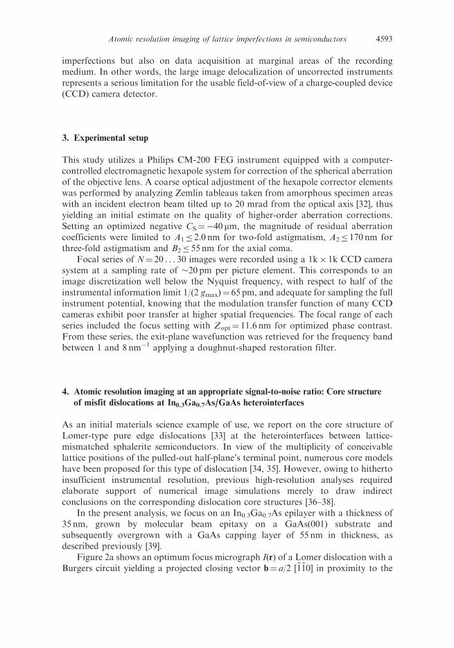
Figure 2a shows an optimum focus micrograph I(r) of a Lomer dislocation with aBurgers circuit yielding a projected closing vector b¼ a/2 ½�1�10� in proximity to the
Atomic resolution imaging of lattice imperfections in semiconductors 4593
interface between the In0.3Ga0.7As epilayer and the GaAs(001) substrate, viewed witha ½1�10� zone-axis orientation of the sample. Far from the dislocation core, the imagecontrast is dominated by clearly separated pairs of contrast dots, constituting atomicdumbbells, at distances of a/4� 141 pm, with a¼ 565 pm denoting the latticeparameter of the substrate material.
However, two conspicuous contrast artefacts become evident fromclose inspection of the Zopt micrograph of the GaAs matrix (Figure 2e).
Figure 2. Analysis of a Lomer-type dislocation with b¼ a/2½�1�10� at an In0.3Ga0.7As/GaAsheterointerface. (a) Optimum focus micrograph I(r) taken along the ½1�10� zone-axis orientationof the sample. (b) ‘Local’ diffraction pattern evaluated from the exit-plane wavefunction of theimage area. (c) Restored phase image �(r). (d) Amplitude image A(r). (e) Magnified clippingof the GaAs-related image area together with the associated phase images �unc(r) and �(r)obtained when neglecting and considering measured residual lens aberrations, respectively.
4594 K. Tillmann et al.
Firstly, non-structure-related spurious intensity peaks are observed between theatomic column positions, which are due to an expanded transfer of low spatialfrequencies at severe phase offsets, especially of the strongly excited {111} beamamplitudes [26]. Secondly, a kidney-shaped distortion of the dumbbells isobserved. As can be seen from quantitative measurements of the associated‘local’ diffraction pattern (figure 2b), these distortions are not due to anypotential misorientation of the sample but instead result from parasitic lensaberrations of A1¼ 2.2 nm (83�), B2¼ 110 nm (83�) and A2¼ 150 nm (43�) withvalues in parentheses indicating the respective azimuth angles inclined in the [001]direction [31]. Thus, the phase �unc(r) of exit-plane wavefunction, retrieved froma focal series of N¼ 30 micrographs and displayed in figure 2e, shows distortionsof the contrast dumbbells when these residual aberrations are not consideredduring the initial step of the reconstruction process. In contrast, the phase image�(r) is free of any distortions after the above-specified aberrations Ai and Bi havebeen eliminated [31].
Moreover, the phase image is also richer in contrast compared to the Zopt
micrograph since there are practically no limitations on temporal and spatialcoherence, thereby providing a superior signal-to-noise ratio at high frequencies upto the information limit. Additionally, the retrieved phase benefits from averaging ofdata from a complete series of micrographs. When quantifying the signal-to-noise-ratios �� and �I of the �(r) and I(r) images, respectively, via the analysis proceduresoutlined in [40], the restoration of the exit-plane wavefunction results in animprovement by a factor of (��/�I)exp¼ 4.1. This value is in excellent agreement withthe ideal factor of (��/�I)th¼
pN/2¼
p30/2¼ 3.9, expected for information retrieval
from a focal series of N¼ 30 micrographs.Also, when determining sample polarity by evaluation of a set of relevant
reciprocal-space amplitudes from the ‘local’ diffraction pattern and subsequenttrimming of simulated data, individual bright contrast dots in the �(r) image may bedirectly associated with gallium and arsenic columns [31]. Corresponding atomicspecies are indicated in figure 2e.
The essential benefit of the combined use of numerical retrieval of the exit-planewavefunction with aberration-corrected imaging, however, becomes evident whenlooking closer at the atomic structure of the dislocation core, which is not resolved inthe single optimum focus image I(r) but only in amplitude and phase images. BothA(r) and �(r) show the atomic arrangement down to the dislocation core and reveala detached atomic column at the intersection of extrapolated lines, indicated by thehorizontal and vertical arrows. Relevant contrast features show mirror symmetrywith respect to the medial (�1�10) lattice plane, indicated by the upright arrows. Thisglobal symmetry continues to the dislocation core.
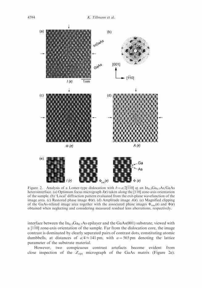
From the exit-plane wavefunction, a core structure model (figure 3a) can bededuced as contrast features are intuitionally interpretable. The dislocation coreshows some similarity to the glide set-type model of a Lomer dislocation,originally proposed by Hornstra [34] which is displayed in figure 3b andcharacterized by an eight-atomic inner ring. The present analysis, however, revealsa less compact core, which is built-up of a 10-sided polygon traversing thedetached atomic column with a different coordination from the surroundingmatrix. This structure also deviates from the complex mirror symmetric
Atomic resolution imaging of lattice imperfections in semiconductors 4595
configurations observed at GaAs/Si interfaces [36, 41] and in Ge/Si heterosystems
[38]. As surface effects in the vicinity of the highly strained dislocation core are
likely to occur in thin electron microscopy specimens, the retrieved core structure
may deviate from that of a dislocation core embedded in bulk material. This
problem, however, exists in any high-resolution analysis involving lattice defects
giving rise to strong lattice distortions.Referring to a detailed discussion in [31], we briefly summarize the causal
connections impeding the resolvability of the dislocation core in the Zopt image but
clearly not in the retrieved exit-plane wavefunction. Numerical image calculations
give clear evidence that this non-resolvability in the single I(r) image is neither due to:
(i) residual image delocalization nor (ii) decreased sample thickness in the vicinity of
the dislocation core. Moreover, the potential impact of (iii) a locally inhomogeneous
strain relaxation of the thin specimen may be ruled out, or, otherwise, the A(r) and
�(r) images would similarly be affected. Instead, the practically improved resolution
of the amplitude and phase images is due to: (iv) increased resistibility against time-
dependant electron beam-induced degeneration of the sample. While numerical
retrieval techniques remove information from intrinsically unstable amorphous
overlayers by averaging, a single Zopt micrograph simply represents a snap-shot of a
Figure 3. Dislocation core models for symmetrical Lomer dislocations. (a) Model retrievedfrom the exit-plane wavefunction displayed in figure 2, together with (b) the symmetrical glide-set-type core model according to Hornstra [34].
4596 K. Tillmann et al.
sample under illumination with a certain probability of an adverse atomic overlayerassembly during the time of exposure [31].
5. Geometric linearity at high-level precession: lattice distortions associated with
dissociated 60� dislocations in GaAs (110)
In sphalerite materials, 60� dislocations with Burgers vectors of type b¼ a/2h0�11imay dissociate into two partials bounding either an intrinsic or extrinsic stackingfault [42–45]. The dissociation reaction is:
a=2½0�11� ! a=6½1�21� þ a=6½�1�12� ð6Þ
with the Burgers vectors of both partials inclining at 30� and 90� to the dislocationline along the ½1�10� direction, respectively. While most analyses of quantitativehigh-resolution microscopy were primarily concerned with distinguishing glide andshuffle set dislocations, i.e. discriminating whether dislocation cores lie on thenarrowly or widely spaced {111} planes by interpreting characteristic contrastfeatures in their vicinity [46–48], it is only recently that efforts have been made toinvestigate the core structure of 30� and 90� partials, both by theoretically applyingab initio calculations [49–51] and experimentally employing advanced electronmicroscopy techniques [53, 53].
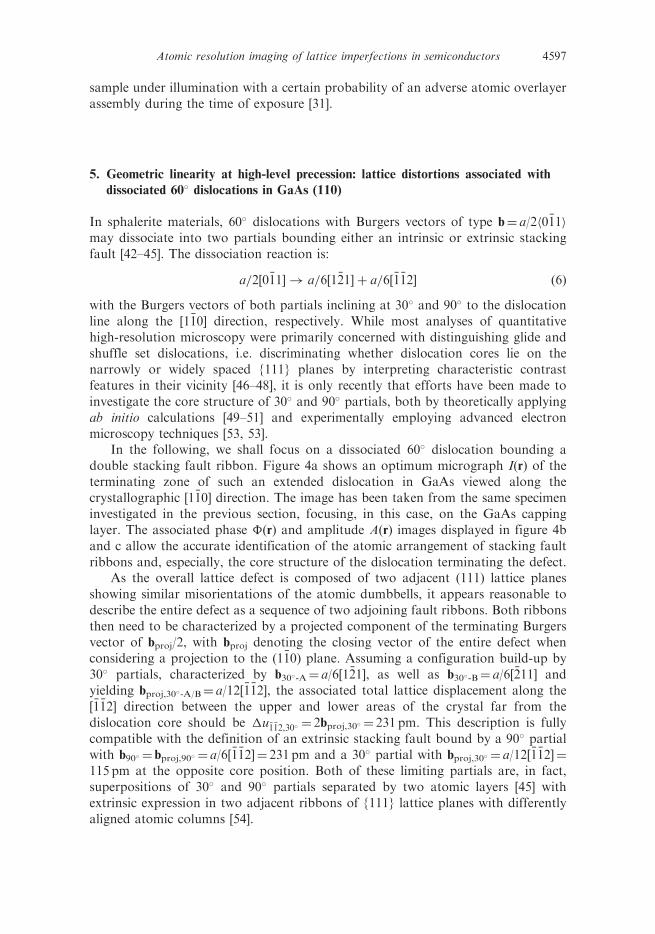
In the following, we shall focus on a dissociated 60� dislocation bounding adouble stacking fault ribbon. Figure 4a shows an optimum micrograph I(r) of theterminating zone of such an extended dislocation in GaAs viewed along thecrystallographic ½1�10� direction. The image has been taken from the same specimeninvestigated in the previous section, focusing, in this case, on the GaAs cappinglayer. The associated phase �(r) and amplitude A(r) images displayed in figure 4band c allow the accurate identification of the atomic arrangement of stacking faultribbons and, especially, the core structure of the dislocation terminating the defect.
As the overall lattice defect is composed of two adjacent (111) lattice planesshowing similar misorientations of the atomic dumbbells, it appears reasonable todescribe the entire defect as a sequence of two adjoining fault ribbons. Both ribbonsthen need to be characterized by a projected component of the terminating Burgersvector of bproj/2, with bproj denoting the closing vector of the entire defect whenconsidering a projection to the (1�10) plane. Assuming a configuration build-up by30� partials, characterized by b30�-A¼ a/6½1�21�, as well as b30�-B¼ a/6½�211� andyielding bproj,30�-A/B¼ a/12½�1�12�, the associated total lattice displacement along the½�1�12� direction between the upper and lower areas of the crystal far from thedislocation core should be �u�1�12,30� ¼ 2bproj,30� ¼ 231 pm. This description is fullycompatible with the definition of an extrinsic stacking fault bound by a 90� partialwith b90� ¼ bproj,90� ¼ a/6½�1�12� ¼ 231 pm and a 30� partial with bproj,30� ¼ a/12½�1�12� ¼115 pm at the opposite core position. Both of these limiting partials are, in fact,superpositions of 30� and 90� partials separated by two atomic layers [45] withextrinsic expression in two adjacent ribbons of {111} lattice planes with differentlyaligned atomic columns [54].
Atomic resolution imaging of lattice imperfections in semiconductors 4597
Figure 4. Analysis of an extrinsic stacking fault in GaAs bound by two adjacent 30� partialdislocations with bproj¼ ½�1�12� in total. (a) High-resolution micrograph I(r) taken under Zopt
conditions. (b) Phase image �(r) and (c) amplitude image A(r) calculated from the associatedfocal series of micrographs. (d) Magnified clipping of �(r) with the positions of atomiccolumns superimposed and the dislocation core positions of 30� partials indicated by redcircles. (e) Contour representation of the lattice displacements along the ½�1�12� direction withreference to the dashed red framed area. (f) Displacement profile measured perpendicular tothe faulted ribbon at the area indicated by the dashed blue frame.
4598 K. Tillmann et al.
To check the validity of this hypothesis, the elastic displacement component u�1�12
along the ½�1�12� direction was evaluated from the �(r) image using geometrical phaseanalysis algorithms [55]. Calculations were performed by applying Gaussian-shapedmasks with decay parameters �¼ |g111|/3 centred around the g111 beams, thusaveraging information over regions of about rdir� 3/(2|g111|)� 490 pm in maximumradius [55]. The correspondingly measured u�1�12(r) distribution is displayed infigure 4e together with a line profile u�1�12(r�1�1�1) extracted from this distribution alongthe ½�1�1�1� direction (figure 4f). For the latter, data values have been averaged over awidth of 1 nm, i.e. over the width of the drawn-in dashed blue frame. The line profileshows two conspicuous plateaus separated by an abrupt discontinuity of�u�1�12 ¼ 234� 60 pm. This value is in excellent agreement with the closing vectorassociated with the 90� partial of an extrinsic stacking fault, for which a total shiftof lattice planes of �u�1�12,30
� ¼ 2bproj,30�-A/B¼ 231 pm is expected (see above). Weemphasize that the specified margin of error in the �u�1�12 value reflectsinhomogeneous lattice distortions of the sample but not the fundamental accuracyto quantify atomic column positions, which may be measured to a precision of abouta few picometres [57, 58].
In figure 4d, single atomic columns, as allocated from the determination of thepolarity of the sample, are superimposed to a magnified clipping of the phase image.Global displacement of the upper and lower crystal areas against each other ismediated by local reorganization of the atomic columns within those two (111)lattice planes, forming the faulted double ribbon. Hence, the associated dislocationcores of both partials, indicated by red circles in the figure, also lie on these (111)planes. As these planes are narrowly spaced, the partial dislocations are of the glideset type. Both dislocation cores are made up of gallium columns leading to aso-called � dislocation [59]. Moreover, the figure also reveals a symmetrical six-foldstructure of the overall dislocation core, which is in perfect agreement with a 90�
partial dislocation composed of two 30� partials separated by two atomic layers [45].Furthermore, we also quantify local distortions of the atomic dumbbells across
the faulted ribbon at some distance of the dislocation core. Thus, contrast dotpositions have been measured from the 5.5� 4.2 nm phase image �(r) area displayedin figure 5a, whose centre is 5.2 nm left of the dislocation core. Therefore, a digitalimage-processing algorithm [60] was applied, which uses: (i) dedicated imageintensity thresholding operations, (ii) a centre-of-mass analysis inside individualbright contrast dots supported by (iii) adequate refining procedures, as specified in[61, 62]. From the measured contrast dot positions, the length and orientation ofindividual dumbbells were calculated and normalized to mean values associated withthe lower (planes # 0–3) and upper (planes # 11–13) areas of the �(r) image. Forstatistical improvement, 15 data points were averaged along the ½�1�12� direction andmedian values plotted in figures 5b and c, dependent on specific (111) lattice planepositions.
As can be seen from both plots, the dumbbells on either side of the double ribbonare rearranged roughly anti-symmetrical in the vicinity of the faulted (111) planes.Thus, the most conspicuous feature is that the dumbbells of the bottom-most latticeplane of the upper crystal domain (plane # 8) are compressed to a length ofhd i¼ 133� 4 pm and turn towards the double ribbon with a misorientation angleh�i� 2.6� 1.3�, compared to the reference lattice planes. In contrast, the uppermost
Atomic resolution imaging of lattice imperfections in semiconductors 4599
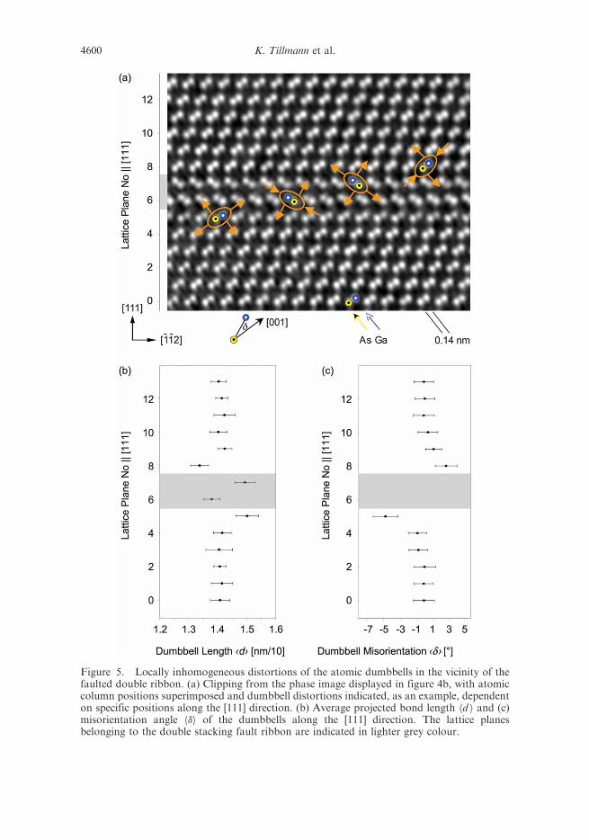
Figure 5. Locally inhomogeneous distortions of the atomic dumbbells in the vicinity of thefaulted double ribbon. (a) Clipping from the phase image displayed in figure 4b, with atomiccolumn positions superimposed and dumbbell distortions indicated, as an example, dependenton specific positions along the [111] direction. (b) Average projected bond length hd i and (c)misorientation angle h�i of the dumbbells along the [111] direction. The lattice planesbelonging to the double stacking fault ribbon are indicated in lighter grey colour.
4600 K. Tillmann et al.
dumbbells of the lower crystal area (plane # 5) are stretched to a length of
hd i¼ 150� 4 pm and bend away from the double ribbon at a misorientation angle of
h�i��4.9� 1.5�.To gauge whether the observed anti-symmetrical distortions represent a genuine
structural property or not, potential implications of scattering and imaging artefacts
need to be eliminated. Since a hypothetic global misalignment of the sample cannot
give rise to any local torsion and dilatation of projected atomic dumbbells, we may
discard this explanation. A similar argument holds true of the potential impact of not
fully compensated aberrations, as they would affect the entire image and, hence,
distort all atomic dumbbells of the same orientation equally. Strictly speaking, any
potential impact of both on-axial and off-axial aberrations needs to be evaluated
separately. In practise, this conceptual differentiation can, however, be ignored due
to the limited field-of-view of the CCD detector and the semi-amplanatic imaging
properties of the double hexapole corrector [13]. Beyond electron-optical analysis, a
supposed strictly anti-symmetric lattice distortion, caused by a dedicated combina-
tion of higher-order aberrations and the faulted ribbon acting incidentally as the
symmetry plane, may be ruled out from a probability point of view due to the large
number of possible combinations, which will not give raise to the observed distortion
behaviour.The observed alteration of atomic dumbbell lengths in the vicinity of stacking
faults ribbons of �10 pm is in fair agreement with recent measurements of lattice
distortions along intrinsic stacking fault ribbons in heavily beryllium-doped GaAs.
This analysis revealed an average expansion of dumbbell lengths up to 158 pm in the
faulted lattice plane, which was explained by segregation of beryllium dopant atoms
and subsequent formation of antisite defects inside of the plane of the faulted ribbon
[53]. Additionally, lattice displacements around the central stacking fault of
Z-shaped dipoles connecting two stair-rod dislocations in indium-doped GaAs
revealed the same anti-symmetric distortion of dumbbell-related contrast dots as
observed in the present analysis. Lateral displacement of gallium and arsenic
atom-pair-related contrast features along the ½�1�12� direction was found to be as much
as 20–50% of the dumbbell length [63].As the specimen in the present study was undoped, we may rule out the
aforementioned explanations, but speculate on indium diffusion from the underlying
In0.3Ga0.7As layer to the GaAs layer along the faulted ribbon. As long as an
inhomogeneous incorporation of indium atoms is not considered, this approach
cannot explain the observed lattice distortions. Admittedly, the anti-symmetric
distortions are perspicuous in elastic distortions associated with the 90� partial
dislocations, which basically follow the measured characteristics of dumbbell
expansion and torsion, but only yield changes in dumbbell lengths smaller than
�3 pm and misorientation angles smaller than � 0.4� for the image area under
investigation [54]. Hence, a more likely explanation could be that the terminating
partial dislocation biases the rearrangement of atomic columns in the vicinity of the
faulted ribbons and that next-but-one neighbour interactions between different
atomic species will play an important role during this process.
Atomic resolution imaging of lattice imperfections in semiconductors 4601
6. Atomic structure of chromium implantation-induced lattice defects in GaN (1120)
As a final example, we report on dislocations introduced by chromium implantation
into GaN. Implantation of transition metals into semiconductors is a candidate
process for the fabrication of diluted magnetic semiconductors for spintronic
applications [64]. A by-product of the implantation is the creation of ion-induced
lattice defects: extrinsic and intrinsic basal plane stacking faults, bounded by Frank
partial or Shockley–Frank partial dislocations, are formed as a result of precipitation
of excess interstitials [54, 65].The GaN films analyzed in this study were grown by metal–organic chemical
vapour deposition on (0001)-oriented sapphire substrates under Si-doping to a
concentration of 2� 1017 cm�3. Crþ ions were implanted with an energy of 200 kV
and a dose of 5� 1016 cm�2 at a temperature of 350�C to avoid amorphization in the
as-implanted samples. A high density of basal plane stacking faults is observed,
besides spherical Cr-rich precipitates, in near-surface regions after chromium
implantation and rapid thermal annealing at 700�C for 5min in N2 atmosphere [66].The majority of basal plane stacking faults are extrinsic bound by Frank partial
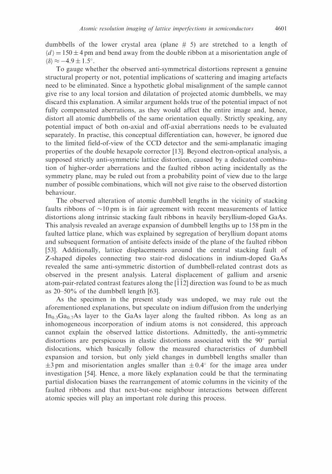
dislocations with Burgers vector b¼ 1/2[0001]. Figure 6 shows the amplitude image
A(r) and phase image �(r) of a perfect nanometre-sized interstitial loop at the
end-range depth of implantation. Gallium and nitrogen columns at a dumbbell
distance of 114 pm, considerably smaller than the information limit of the
instrument, are not fully resolved. Nonetheless, the N-polarity is unambiguously
visible from the directly interpretable bright contrast in the phase image. Tetrahedral
coordination across the faulted layer stacking is confirmed, asserting that no foreign
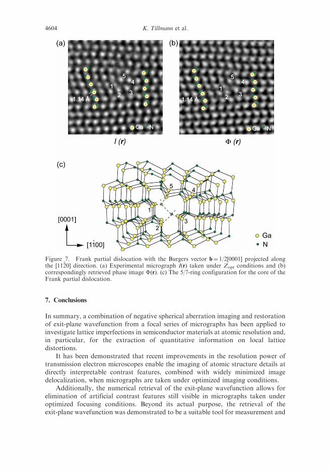
chromium–gallium alloy phase is connected with the planar defects.A magnified view of the core of a Frank partial dislocation at the terminating
zone of several tens of nanometers large dislocation loop is shown in the Zopt and
�(r) images retrieved from a corresponding focal series (figures 7a and b). Although
the I(r) and �(r) appear very similar, the improved signal-to-noise ratio in the phase
image enhances the visibility of the nitrogen positions and dumbbell orientation up
to the core of the dislocation. The phase image �(r) strengthens the presence of
further nitrogen atoms within the core surrounded by the cage of the five marked
gallium columns. The faint phase shift in �(r), in which non-linear image
components and image delocalization are eliminated, indicates a nitrogen-filled
core, in favour of a chromium- or gallium-rich core.Based on these observations, a tentative 5/7 ring configuration for the core is
presented in figure 7c. The nitrogen atoms shared by the five- and seven-membered
rings are three-fold coordinated with Ga and N. Due to the wrong bond and the
presence of unpaired electrons, this structure is not expected to be the most stable
configuration. Since �(r) is retrieved from a focal series taken over a period of a few
ten of seconds, the image conceivably reflects a transient state of the core that gathers
further interstitials during observation. The Zopt image level may, therefore, contain
complementary, but not necessarily identical, information when compared to �(r).
Indeed, in the present case, the Zopt image, with its inferior noise level compared to
�(r), also implies an alternative structure, which contains two wrong Ga–Ga bonds
connecting three-fold coordinated Ga atoms at positions 1–5 and 2–3, respectively.
4602 K. Tillmann et al.
Figure 6. Interstitial loop in Cr-implanted GaN viewed along the ½11�20� direction. (a)Amplitude image A(r) and (b) phase image �(r) calculated from a focal series of micrographs.Simulated images of the periodic N-polarity GaN structure assuming a sample thickness of3.2 nm at a resolution of 7.5 nm�1 are superimposed in the lower left part of the images.The stacking sequence is ABABCABAB, where the underlined section highlights sphaleritestacking.
Atomic resolution imaging of lattice imperfections in semiconductors 4603
7. Conclusions
In summary, a combination of negative spherical aberration imaging and restorationof exit-plane wavefunction from a focal series of micrographs has been applied toinvestigate lattice imperfections in semiconductor materials at atomic resolution and,in particular, for the extraction of quantitative information on local latticedistortions.
It has been demonstrated that recent improvements in the resolution power oftransmission electron microscopes enable the imaging of atomic structure details atdirectly interpretable contrast features, combined with widely minimized imagedelocalization, when micrographs are taken under optimized imaging conditions.
Additionally, the numerical retrieval of the exit-plane wavefunction allows forelimination of artificial contrast features still visible in micrographs taken underoptimized focusing conditions. Beyond its actual purpose, the retrieval of theexit-plane wavefunction was demonstrated to be a suitable tool for measurement and
Figure 7. Frank partial dislocation with the Burgers vector b¼ 1/2[0001] projected alongthe ½11�20� direction. (a) Experimental micrograph I(r) taken under Zopt conditions and (b)correspondingly retrieved phase image �(r). (c) The 5/7-ring configuration for the core of theFrank partial dislocation.
4604 K. Tillmann et al.
numerical correction of residual lens aberrations, as well as for proper orientation ofspecimens during TEM operation.
In addition to the individual advantages of either technique, their combined useallows the accurate identification of lattice imperfections in semiconductor materialsat hitherto unequalled imaging quality. Experimental analyses clearly benefit fromusing aberration-corrected input data, i.e. from an increase in instrumentalinformation limit together with a decrease in image delocalization and a pre-reduction in lens aberrations, as well as from the complete elimination of residualaberrations by numerical retrieval of the exit-plane wavefunction, which is also freefrom non-linear imaging artefacts and yields images characterized by an appropriatesignal-to-noise ratio.
By the deliberate combination of both techniques, Lomer dislocation cores atIn0.3Ga0.7As/GaAs heterointerfaces have been imaged at atomic resolution anddirectly identified as being composed of a mirror symmetric 10-atomic ring, thusrendering extensive image simulations superfluous. Quantification of local latticedistortions in the vicinity of a double stacking fault ribbon in GaAs by analysis ofexperimental phase images �(r) shows clear evidence of anti-symmetric torsion andexpansion of atomic dumbbells with respect to the faulted ribbon. A similarquantitative analysis, focusing on lattice imperfections in GaN at atomic resolutionbased on the synergetic combination of negative spherical aberration-correctedimaging and numerical retrieval of the exit-plane wavefunction, is presentlyhampered by instrumental resolution but will soon be possible with aberration-corrected sub-Angstrom resolution microscopes.
Acknowledgements
The authors are grateful to Arno Forster and Vitaly Guzenko for making availablethe samples investigated in this study, as well as Doris Meertens for specimenpreparation work.
References
[1] H. Alexander and H. Teichler, in Handbook of Semiconductor Technology, edited byK.A. Jackson and W. Schroter, Vol. 1 (Wiley-VCH, New York, 2000), pp. 291–376.
[2] R. Jones, Mater. Sci. Eng. B 71 24 (2000).[3] P.B. Hirsch, Mater. Sci. Technol. 1 666 (1985).[4] S.P. Beckmann and D.C. Chrzan, Physica B 340/342 1001 (2003).[5] C. Kisielowski, C.J.D. Hetherington, Y.C. Wang, et al., Ultramicroscopy 89 243 (2001).[6] M.A. O’Keefe, E.C. Nelson, E.C. Wang, et al., Phil. Mag. B 71 1861 (2001).[7] B. Freitag, S. Kujawa, P.M. Mul, et al., Ultramicroscopy 102 209 (2005).[8] C.L. Jia, M. Lentzen and K. Urban, Science 299 870 (2003).[9] C.L. Jia, M. Lentzen and K. Urban, Microsc. Microanal. 10 174 (2004).[10] J.L. Hutchison, J.M. Titchmarsh, D.J.H. Cockayne, et al., Ultramicroscopy 103 7 (2005).[11] H. Lichte, Ultramicroscopy 38 13 (1991).[12] W. Coene and A.J.E.M. Jansen, Scan. Microsc. Suppl. 6 379 (1992).[13] H. Rose, Optik 85 19 (1990).[14] M. Haider, H. Rose, S. Uhlemann, et al., Nature 392 768 (1998).
Atomic resolution imaging of lattice imperfections in semiconductors 4605
[15] M. Lentzen, B. Jahnen, C.L. Jia, et al., Ultramicroscopy 92 233 (2002).[16] W.M.J. Coene, G. Janssen, M. Op de Beeck, et al., Phys. Rev. Lett. 69 3743 (1992).[17] W.M.J. Coene, A. Thust, M. Op de Beeck, et al., Ultramicroscopy 64 109 (1996).[18] A. Thust, W.M.J. Coene, M. Op de Beeck, et al., Ultramicroscopy 64 211 (1996).[19] A.I. Kirkland, W.O. Saxton, K.L. Chau, et al., Ultramicroscopy 57 355 (1995).[20] A.I. Kirkland, W.O. Saxton and G. Chand, J. Electron Microsc. 1 11 (1997).[21] A. Thust, M.H.F. Overwijk, W.M.J. Coene, et al., Ultramicroscopy 64 249 (1996).[22] A. Thust, C.L. Jia and K. Urban, in Proceedings ICEM-15, edited by R. Cross, Vol. 1
(Microscopy Society of Southern Africa, Durban, 2002), pp. 167–168.[23] R.R. Meyer, A.I. Kirkland and W.O. Saxton, Ultramicroscopy 92 89 (2002).[24] R.R. Meyer, A.I. Kirkland and W.O. Saxton, Ultramicroscopy 99 115 (2004).[25] D.B. Williams and C.B. Carter, Transmission Electron Microscopy (Plenum Press,
New York, 1996).[26] M. Lentzen, Ultramicroscopy 99 211 (2004).[27] S. Uhlemann and M. Haider, Ultramicroscopy 72 109 (1998).[28] M.A. O’Keefe, C.J.D. Hetherington, Y.C. Wang, et al., Ultramicroscopy 89 215 (2001).[29] L.Y. Chang, F.R. Chen, A.I. Kirkland, et al., J. Electron Microsc. 52 359 (2003).[30] R.R. Meyer, A.I. Kirkland and W.O. Saxton, Ultramicroscopy 99 115 (2004).[31] K. Tillmann, A. Thust and K. Urban, Microsc. Microanal. 10 185 (2004).[32] F. Zemlin, K. Weiss, P. Schiske, et al., Ultramicroscopy 3 49 (1978).[33] W.M. Lomer, Phil. Mag. 42 1327 (1951).[34] J. Hornstra, J. Phys. Chem. Solids 5 129 (1958).[35] A. Bourret, J. Dessaux and R. Renault, Phil. Mag. A 45 1 (1982).[36] A. Vila, A. Cornet, J.R. Morante, et al., Phil. Mag. A 75 85 (1995).[37] D. Wang, H. Chen, F.H. Li, et al., Ultramicroscopy 93 139 (2002).[38] J.N. Stirman, P.A. Crozier, D.J. Smith, et al., Appl. Phys. Lett. 84 2530 (2004).[39] K. Tillmann and A. Forster, Thin Solid Films 368 93 (2000).[40] L. Houben, A. Thust and K. Urban, Ultramicroscopy 106 200 (2006).[41] S. Lopatin, S.J. Pennycook, J. Narayan, et al., Appl. Phys. Lett. 81 2728 (2002).[42] F.C. Frank, Phil. Mag. 42 809 (1951).[43] I.L.F. Ray and D.J.H. Cockayne, Proc. R. Soc. A 325 543 (1971).[44] P. Gai and A. Howie, Phil. Mag. 30 939 (1974).[45] S. Amelinckx, in Dislocations in Solids, edited by F.R.N. Nabarro, Vol. 2
(North-Holland, Amsterdam, 1979), pp. 67–460.[46] A. Olsen and J.C.H. Spence, Phil. Mag. A 43 945 (1981).[47] M. Tanaka and B. Jouffrey, Phil. Mag. A 50 733 (1984).[48] B.C. de Cooman and D.B. Carter, Phys. Status Solidi (a) 112 473 (1989).[49] R.W. Nunes, J. Bennetto and D. Vanderbilt, Phys. Rev. B 58 12563 (1998).[50] J.F. Justo, R.W. Nunes and L.V.C. Assali, J. Phys.: Condens. Matter 14 12749 (2002).[51] S.P. Beckman, X. Xu, P. Specht, et al., J. Phys.: Condens. Matter 14 12673 (2002).[52] H.R. Kolar, J.C.H. Spence and H. Alexander, Phys. Rev. Lett. 77 4031 (1996).[53] X. Xu, S.P. Beckmann, P. Specht, et al., Phys. Rev. Lett. 95 145501 (2005).[54] J.P. Hirth and J. Lothe, Theory of Dislocations (McGraw Hill, New York, 1968).[55] M.J. Hytch, E. Snoeck and R. Kilaas, Ultramicroscopy 74 131 (1998).[56] J.L. Rouviere and E. Sarigiannidou, Ultramicroscopy 106 1 (2005).[57] C.L. Jia and A. Thust, Phys. Rev. Lett. 82 5052 (1999).[58] M.J. Hytch, J.L. Putax and J.M. Penisson, Nature 423 279 (2003).[59] A.M. Gomez and P.B. Hirsch, Phil. Mag. A 38 733 (1978).[60] K. Tillmann, M. Lentzen and R. Rosenfeld, Ultramicroscopy 83 111 (2000).[61] R. Kilaas, S. Paciornik, A.J. Schwartz, et al., J. Comput.-Assist. Microsc. 6 129 (1994).[62] H. Seitz, K. Ahlborn, M. Seibt, et al., J. Microsc. 190 184 (1997).[63] S.H. Lim, D. Shindo, I. Yonenaga, et al., Phys. Rev. Lett. 81 5350 (1998).[64] H. Ohno, Science 281 951 (1998).[65] V. Kirchner, H. Heinke, U. Birkle, et al., Phys. Rev. B 58 15749 (1998).[66] V.A. Guzenko, N. Thillosen, A. Dahmen, et al., J. Appl. Phys. 96 5663 (2004).
4606 Atomic resolution imaging of lattice imperfections in semiconductors