Crystal Lattice Imperfections There are four types of crystal lattice imperfections : 1....
16
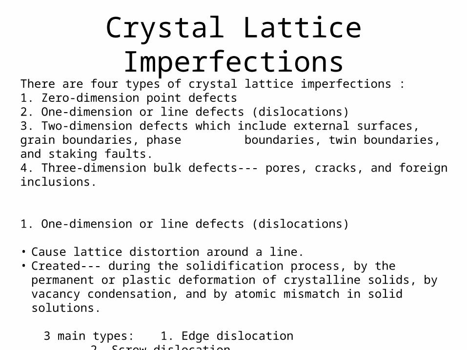
Crystal Lattice Imperfections There are four types of crystal lattice imperfections : 1. Zero-dimension point defects 2. One-dimension or line defects (dislocations) 3. Two-dimension defects which include external surfaces, grain boundaries, phase boundaries, twin boundaries, and staking faults. 4. Three-dimension bulk defects--- pores, cracks, and foreign inclusions. 1. One-dimension or line defects (dislocations) • Cause lattice distortion around a line. • Created--- during the solidification process, by the permanent or plastic deformation of crystalline solids, by vacancy condensation, and by atomic mismatch in solid solutions. 3 main types: 1. Edge dislocation 2. Screw dislocation
-
Upload
cecilia-matis -
Category
Documents
-
view
234 -
download
1
Transcript of Crystal Lattice Imperfections There are four types of crystal lattice imperfections : 1....
Crystal Lattice ImperfectionsThere are four types of crystal lattice imperfections :1. Zero-dimension point defects2. One-dimension or line defects (dislocations)3. Two-dimension defects which include external surfaces, grain boundaries, phase boundaries, twin boundaries, and staking faults.4. Three-dimension bulk defects--- pores, cracks, and foreign inclusions.
1. One-dimension or line defects (dislocations)
• Cause lattice distortion around a line.• Created--- during the solidification process, by the permanent or plastic
deformation of crystalline solids, by vacancy condensation, and by atomic mismatch in solid solutions.
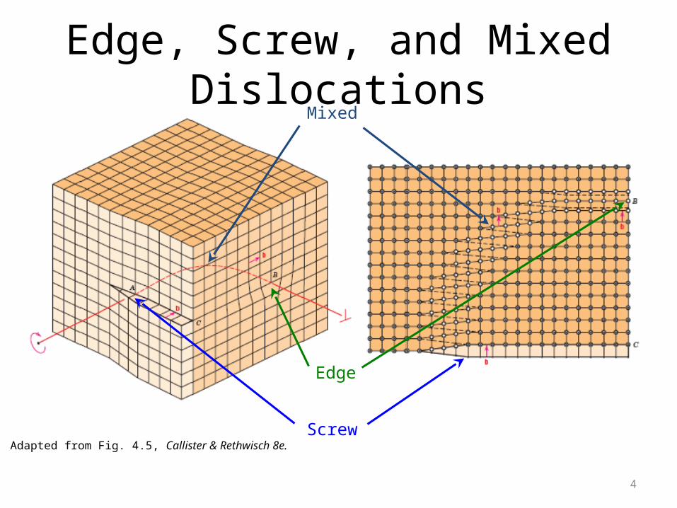
3 main types: 1. Edge dislocation2. Screw dislocation3. Combination of the two--- Mixed dislocation.
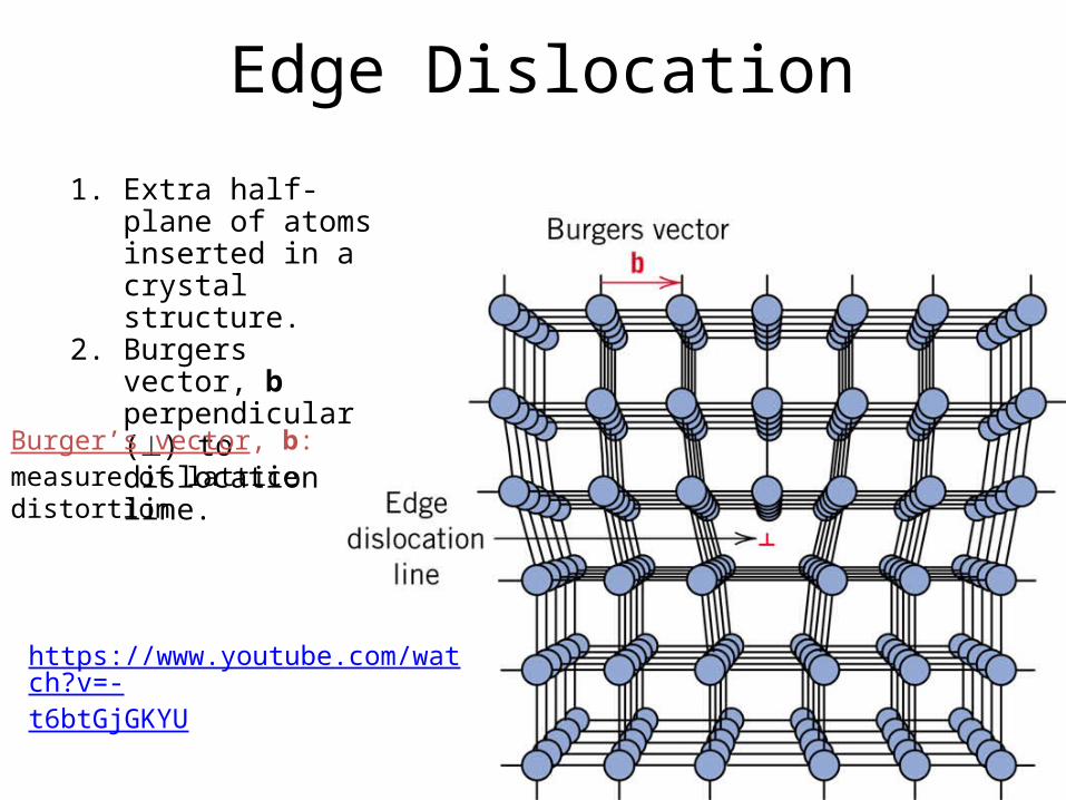
Edge Dislocation
1. Extra half-plane of atoms inserted in a crystal structure.
2. Burgers vector, b perpendicular () to dislocation line.
Burger’s vector, b: measure of lattice distortion
https://www.youtube.com/watch?v=-t6btGjGKYU
3
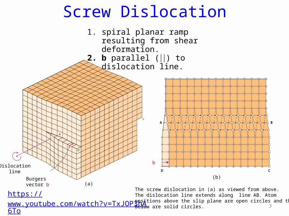
Screw Dislocation
Screw Dislocation
The screw dislocation in (a) as viewed from above.The dislocation line extends along line AB. Atom positions above the slip plane are open circles and those Below are solid circles.
Burgers vector b
Dislocationline
b
(a)(b)
1. spiral planar ramp resulting from shear deformation.
2. b parallel () to dislocation line.
https://www.youtube.com/watch?v=TxJOP3hA6To
4
Edge, Screw, and Mixed Dislocations
Adapted from Fig. 4.5, Callister & Rethwisch 8e.
Edge
Screw
Mixed
5
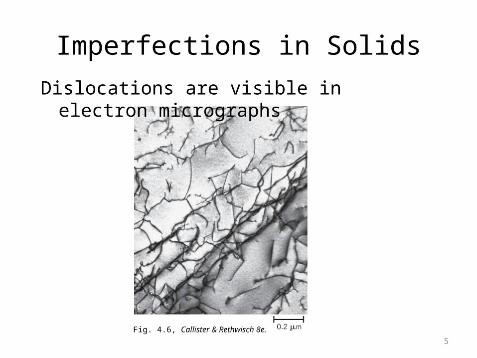
Imperfections in SolidsDislocations are visible in electron micrographs
Fig. 4.6, Callister & Rethwisch 8e.
6
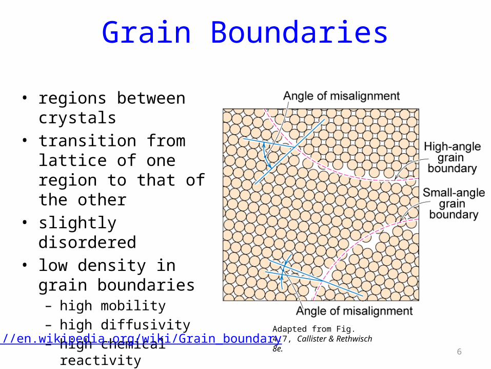
Grain Boundaries
• regions between crystals• transition from lattice of
one region to that of the other
• slightly disordered• low density in grain
boundaries– high mobility– high diffusivity– high chemical reactivity
Adapted from Fig. 4.7, Callister & Rethwisch 8e.http://en.wikipedia.org/wiki/Grain_boundary
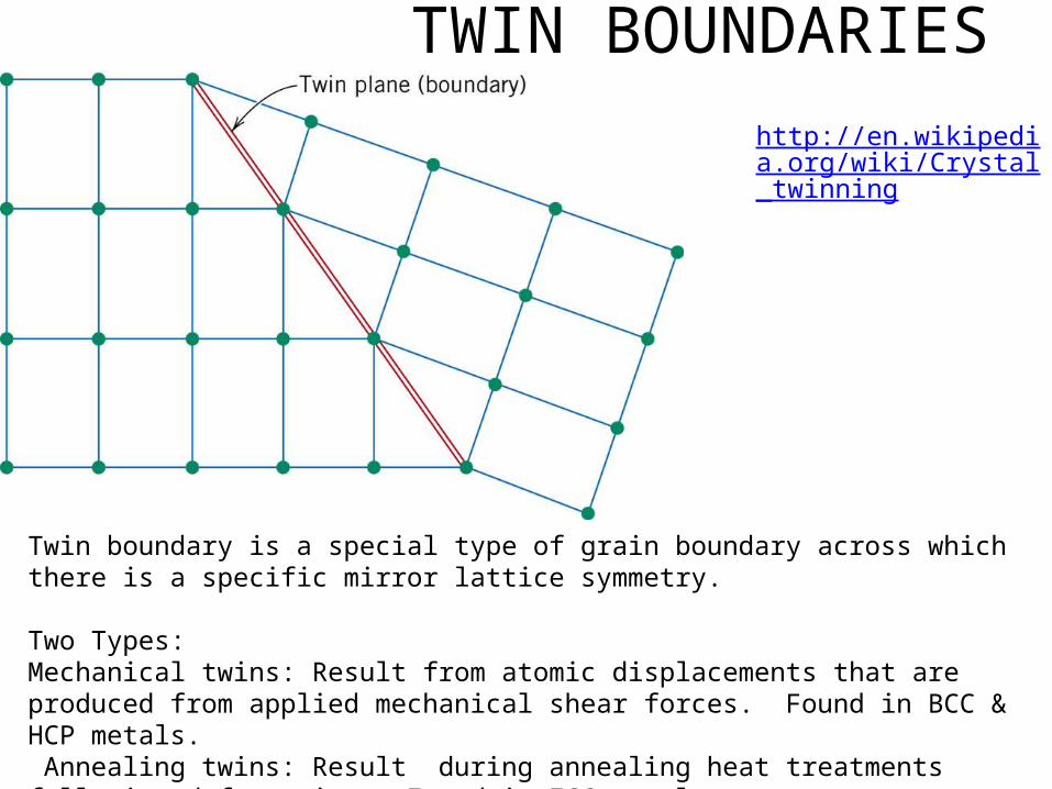
TWIN BOUNDARIES
Twin boundary is a special type of grain boundary across which there is a specific mirror lattice symmetry. Two Types:Mechanical twins: Result from atomic displacements that are produced from applied mechanical shear forces. Found in BCC & HCP metals. Annealing twins: Result during annealing heat treatments following deformation. Found in FCC metals.
http://en.wikipedia.org/wiki/Crystal_twinning

8
Microscopic Examination
• Crystallites (grains) and grain boundaries. Vary considerably in size. Can be quite large.– ex: Large single crystal of quartz or diamond or Si– ex: Aluminum light post or garbage can - see the
individual grains
• Crystallites (grains) can be quite small (mm or less) – necessary to observe with a microscope.
9
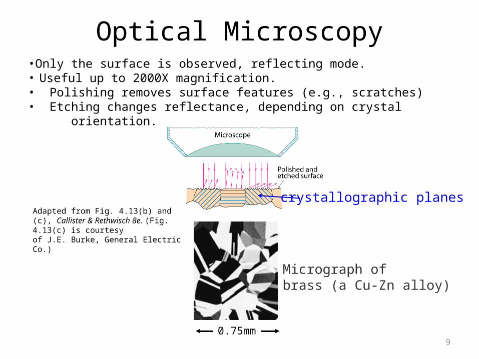
•Only the surface is observed, reflecting mode.• Useful up to 2000X magnification.• Polishing removes surface features (e.g., scratches)• Etching changes reflectance, depending on crystal orientation.
Micrograph ofbrass (a Cu-Zn alloy)
0.75mm
Optical Microscopy
Adapted from Fig. 4.13(b) and (c), Callister & Rethwisch 8e. (Fig. 4.13(c) is courtesyof J.E. Burke, General Electric Co.)
crystallographic planes
10
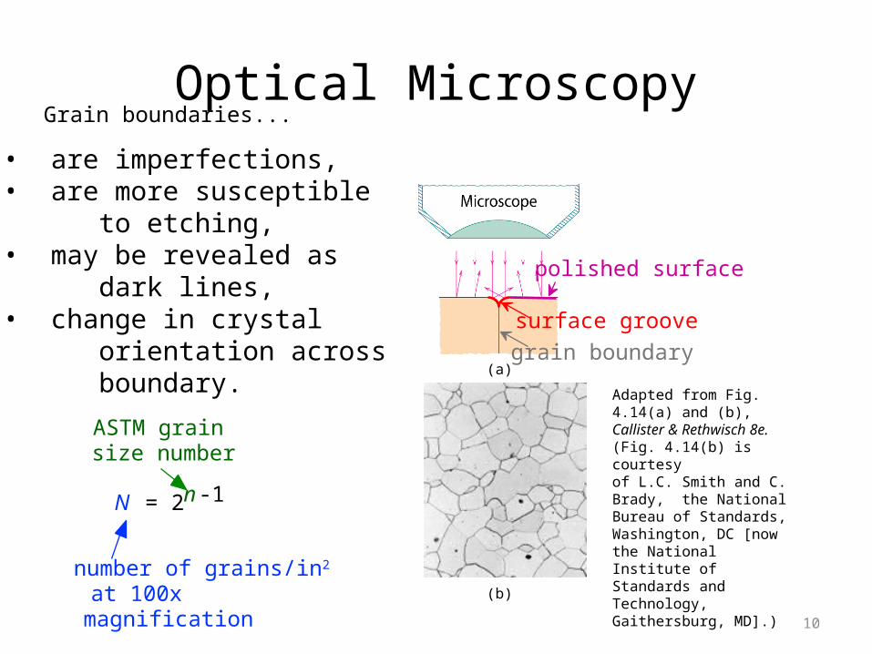
Grain boundaries...
• are imperfections,• are more susceptible to etching,• may be revealed as dark lines,• change in crystal orientation across boundary. Adapted from Fig. 4.14(a) and
(b), Callister & Rethwisch 8e.(Fig. 4.14(b) is courtesyof L.C. Smith and C. Brady, the National Bureau of Standards, Washington, DC [now the National Institute of Standards and Technology, Gaithersburg, MD].)
Optical Microscopy
ASTM grain size number
N = 2 n -1
number of grains/in2 at 100x magnification
Fe-Cr alloy
(b)
grain boundarysurface groove
polished surface
(a)
11
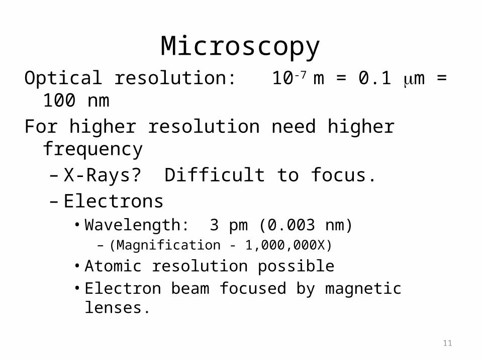
MicroscopyOptical resolution: 10-7 m = 0.1 m = 100 nmFor higher resolution need higher frequency
– X-Rays? Difficult to focus.– Electrons
• Wavelength: 3 pm (0.003 nm) – (Magnification - 1,000,000X)
• Atomic resolution possible• Electron beam focused by magnetic lenses.
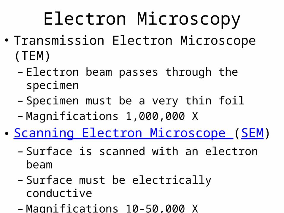
Electron Microscopy• Transmission Electron Microscope (TEM)
– Electron beam passes through the specimen– Specimen must be a very thin foil– Magnifications 1,000,000 X
• Scanning Electron Microscope (SEM)– Surface is scanned with an electron beam– Surface must be electrically conductive– Magnifications 10-50,000 X– Elemental composition of very localized surface areas
are possible• http://www.youtube.com/watch?v=5qcJySNLs84&feature=related• http://www.youtube.com/watch?v=VH5H6uSQUFE
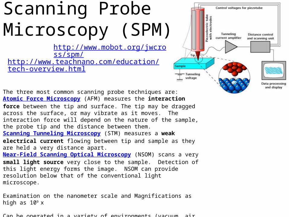
Scanning Probe Microscopy (SPM)
http://www.mobot.org/jwcross/spm/
http://www.teachnano.com/education/tech-overview.html
The three most common scanning probe techniques are: Atomic Force Microscopy (AFM) measures the interaction force between the tip and surface. The tip may be dragged across the surface, or may vibrate as it moves. The interaction force will depend on the nature of the sample, the probe tip and the distance between them. Scanning Tunneling Microscopy (STM) measures a weak electrical current flowing between tip and sample as they are held a very distance apart. Near-Field Scanning Optical Microscopy (NSOM) scans a very small light source very close to the sample. Detection of this light energy forms the image. NSOM can provide resolution below that of the conventional light microscope.
Examination on the nanometer scale and Magnifications as high as 109 x
Can be operated in a variety of environments (vacuum, air, liquid, etc)
14
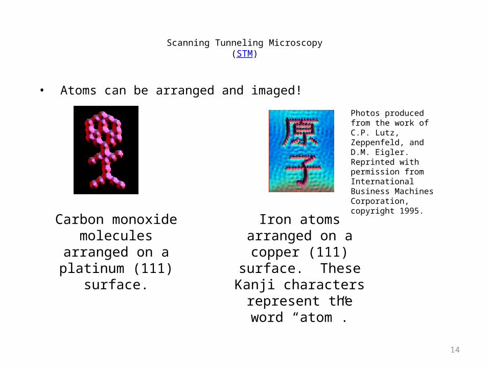
• Atoms can be arranged and imaged!
Carbon monoxide molecules arranged on
a platinum (111) surface.
Photos produced from the work of C.P. Lutz, Zeppenfeld, and D.M. Eigler. Reprinted with permission from International Business Machines Corporation, copyright 1995.
Iron atoms arranged on a copper (111) surface. These Kanji characters
represent the word “atom”.
Scanning Tunneling Microscopy(STM)

16
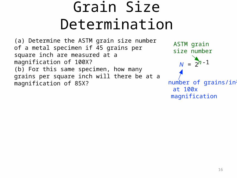
Grain Size Determination
ASTM grain size number
N = 2 n -1
number of grains/in2 at 100x magnification
(a) Determine the ASTM grain size number of a metal specimen if 45 grains per square inch are measured at a magnification of 100X?(b) For this same specimen, how many grains per square inch will there be at a magnification of 85X?


![Crystal Imperfections in Solids [7] - Unesp · Crystal Imperfections in Solids 3> ¾The atomic arrangements in a crystalline lattice is almost always not perfect. ¾There are “defects”](https://static.fdocuments.net/doc/165x107/5eb9eed0c37e1e5d6524b706/crystal-imperfections-in-solids-7-unesp-crystal-imperfections-in-solids-3.jpg)