Amplifier frequency response (part 2)
50
Engr.Tehseen Ahsan Lecturer, Electrical Engineering Department EE-307 Electronic Systems Design HITEC University Taxila Cantt, Pakistan Amplifier Frequency Response (Part 2)
-
Upload
jamil-ahmed-khan -
Category
Engineering
-
view
321 -
download
9
Transcript of Amplifier frequency response (part 2)

Engr.Tehseen Ahsan
Lecturer, Electrical Engineering Department
EE-307 Electronic Systems Design
HITEC University Taxila Cantt, Pakistan
Amplifier Frequency Response
(Part 2)

The Bode Plot A plot of dB voltage gain versus frequency on semilog paper
is called a Bode Plot.
A generalized Bode plot for an RC circuit like that shown in
figure 10-23 (a) appears in part (b)
2

The Bode Plot continue… The ideal response curve is shown in blue. Notice that it is
flat (0 dB) down to critical frequency at which point the gain
drops at -20 dB/decade.
Above fc are the mid range frequencies. The actual response
curve is shown in red.
The actual response curve decreases gradually in midrange
and is down to -3 dB at the critical frequency.
Often, the ideal response is used to simplify amplifier analysis
The critical frequency at which the curve breaks into a -20
dB/decade drop is sometimes called the lower break frequency.
3

Total Low-Frequency Response of an Amplifier
Let’s look at the combined effect of the three High-pass RC
circuits in a BJT amplifier.
Each circuit has a critical frequency determined by R and C
values.
The critical frequencies of the three RC circuits are not
necessarily all equal.
If one of the RC circuits has a critical (break) frequency
higher than the other two then it is the dominant RC circuit.
The dominant circuit determines the frequency at which the
overall gain of amplifier begins to drop at-20 dB/decade.
The other circuits each cause an additional -20 dB/decade
roll-off below their respective critical (break) frequencies.4

Total Low-Frequency Response of an Amplifier continue…
5

Total Low-Frequency Response of an Amplifier continue…
Refer to Bode plot in figure 10-25 which shows the
superimposed ideal responses for three RC circuits (green
Lines) of a BJT amplifier.
Each RC circuit has a different critical frequency.
The input RC circuit is dominant (highest fc ) in this case, and
the bypass RC circuit has the lowest fc . The overall response
is shown as the blue line.
6

Total Low-Frequency Response of an Amplifier continue…
7

Total Low-Frequency Response of an Amplifier continue…
Refer to the Bode plot in figure 10-26 all RC circuits have
the same critical frequency, the response curve has one break
point at that value of fc , and the voltage gain rolls off at -60
dB/decade below that value.
In this case the gain is at -9 dB below the midrange voltage
gain( -3 dB for each RC circuit).
8

9

10

11

10-4 High-Frequency Amplifier Response We have seen the coupling and bypass capacitors affect the
voltage gain of an amplifier at lower frequencies where the
reactances of the coupling and bypass capacitors are
significant.
In midrange of an amplifier, the effects of the capacitors are
minimal and can be neglected.
If the frequency is increased sufficiently, a point is reached
where the transistor’s internal capacitances began to have a
significant effect on the gain.
12

BJT Amplifiers A high-frequency ac equivalent circuit for the BJT amplifier
in fig 10-31(a) is shown in fig10-31(b).
13

BJT Amplifiers continue… Notice that the coupling and bypass capacitors are treated as
effective shorts and don’t appear in equivalent circuit.
The internal capacitances Cbe and Cbc , which are significant
only at high frequencies, do appear in the diagram.
Cbe is sometimes called input capacitance Cib , and Cbc is
sometimes called output capacitance Cob.
Cbe is specified on datasheets at a certain value of VBE.
Often the datasheet will list Cib as Cibo and Cob as Cobo.
The o as the letter in the subscript indicates the capacitance is
measured with the base open.
14

Miller’s Theorem in High-Frequency Analysis
(in BJT Amplifiers) Cin(Miller) = Cbc(Av+1)
Cout(Miller) = Cbc(Av+1/Av)
These two Miller capacitances (Cin(Miller) & Cout(Miller))create a
high-frequency input RC circuit and a high-frequency output
RC circuit.
Because the capacitances go to ground and therefore act as
low-pass filters.
15
Ideal Model because
stray capacitances due to
circuit interconnections
are neglected

The Input RC Circuit At high frequencies, the input circuit is shown in fig 10-33(a)
where Rin(base)= βac r'e
16

The Input RC Circuit continue… As the frequency increases, the capacitive reactance becomes
smaller. This causes the signal voltage at base to decrease, so
the amplifier’s voltage gain decreases.
The reason for this is that the capacitance and resistance act
as a voltage divider and, as the frequency increases, more
voltage is dropped across the resistance and less across
capacitance.
At the critical frequency, the gain is 3 dB less than its
midrange value.
The critical high frequency , fc, is the frequency at which the
capacitive reactance is equal to the total resistance.
XC tot= Rth = Rout= Rs ∥ R1 ∥ R2 ∥ βac r'e17

The Input RC Circuit continue…
18
Upper critical Frequency

19

20

21

Phase Shift of the Input RC Circuit Because the output voltage of a high-frequency input RC
circuit is across the capacitor, the output voltage lags the
input.The phase angle is expressed as
At the critical frequency fc, the phase angle is 45˚ with the
base (output) voltage lagging the input signal.
As the frequency increases above, the phase angle increases
above 45˚ and approaches 90˚ when the frequency is
sufficiently high.
22
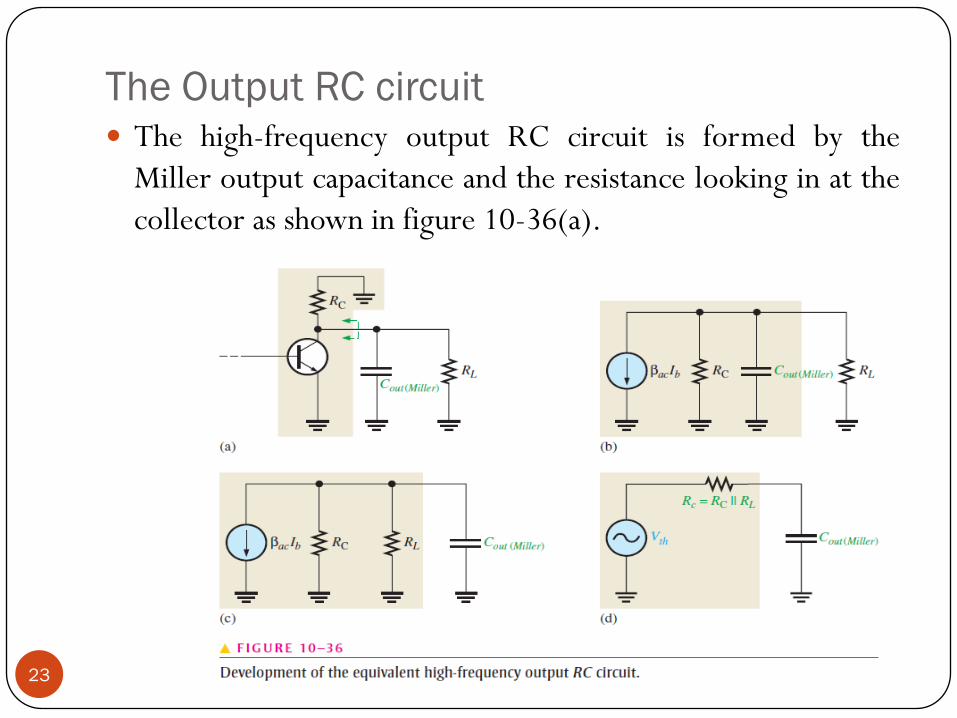
The Output RC circuit The high-frequency output RC circuit is formed by the
Miller output capacitance and the resistance looking in at the
collector as shown in figure 10-36(a).
23

The Output RC circuit continue… Cout(Miller) = Cbc(Av+1/Av)
If the voltage gain is at least 10, then Cout(Miller) ≈ Cbc.
The critical frequency is determined as
Just like input RC circuit, the output RC circuit reduces the
gain by 3 dB at the critical frequency. When the frequency
goes above the critical value, the gain drops at -20 dB/decade
rate.The phase angle introduced by output RC circuit is
24
Where Rc = RC ∥ RL

25

26

FET Amplifiers The approach to the high-frequency analysis of a FET
amplifier is similar to that of a BJT.
The basic differences are the specifications of the internal
FET capacitances and the determination of the input
resistance. Figure 10-39(a) shows a JFET common-source
amplifier used to illustrate high-frequency analysis.
27

FET Amplifiers Continue… A high-frequency equivalent circuit for the amplifier is shown
in figure 10-39(b).
The coupling and bypass capacitors are assumed to have
negligible reactances and are considered to be shorts.
The internal capacitances Cgs and Cgd appear in the equivalent
circuit because their reactances are significant at high
frequencies.
28

Values of Cgs, Cgd, and Cds FET data sheets do not normally provide values for Cgs, Cgd,
or Cds.
Instead three other values are usually specified with the help
of them you can easily calculate Cgs, Cgd, and Cds.
Cgd= Crss Cgs= Ciss - Crss Cds= Coss- Crss
Coss is not specified as often as the other values on data sheets.
In cases where Coss is not available, you must either assume a
value or neglect Cds.
29
Ciss = the input capacitance
Crss = the reverse transfer capacitance
Coss= the output capacitance

Miller’s Theorem in High-Frequency Analysis (in FET
Amplifiers)
Cin(Miller) = Cgd(Av+1)
Cout(Miller) = Cgd(Av+1/Av)
These two Miller capacitances (Cin(Miller) & Cout(Miller))create a
high-frequency input RC circuit and a high-frequency output
RC circuit.
Both are low-pass filters which produce phase lag.
30

The Input RC Circuit The high-frequency input circuit forms a low-pass type of
filter and is shown in fig-10-41(a).
31

The Input RC Circuit Continue… Since both RG and Rin(gate) of FETs are extremely high,
therefore controlling resistance for the input circuit is the
resistance of the input source Rs as long as Rs<< Rin.
This is because Rs appears in parallel with Rin when Thevenin’s
theorem is applied.
The simplified input RC circuit appears in figure 10-41(b).
The critical frequency is :
32

33

34

The Output RC circuit The high-frequency output RC circuit is formed by the
Miller output capacitance and the resistance looking in at the
drain as shown in figure 10-43(a).
35

The Output RC circuit continue… Cout(Miller) = Cgd(Av+1/Av)
If the voltage gain is at least 10, then Cout(Miller) ≈ Cgd.
The critical frequency is determined as
The output circuit produces a phase shift of
36
Where Rd = RD ∥ RL

37

Total High-Frequency Response of an Amplifier
We have already seen that, two RC circuits (Cin(Miller)&
Cout(Miller)) created by the internal transistor capacitances
influence the high-frequency response of both BJT and FET.
As the frequency increases and reaches the high end of its
midrange values, one of the RC circuit will cause the
amplifier’s gain to begin dropping off.
The frequency at which this occurs is the dominant critical
frequency; it is the lower of the two critical frequencies.
An ideal high-frequency Bode plot is shown in figure 10-
44(a) next slide. It shows the first break point at fcu(input)where the voltage gain begins to roll off at -20 dB/decade. At
fcu(output) , the gain begins dropping at -40 dB/decade because
each RC circuit is adding a -20 dB/decade roll-off38

Total High-Frequency Response of an Amplifier continue…
Figure 10-44(b) shows a non-ideal Bode plot where the
voltage gain is actually -3 dB below midrange at fcu(input) .
Other possibilities are that the output RC circuit is dominant
or both circuits have the same critical frequency.
39

10-5 Total Amplifier Frequency Response Figure 10-45(b) next slide shows a generalized ideal Bode plot for
the BJT amplifier in fig 10-45(a) next slide.
The three break points at the lower critical frequencies (fcl1 , fcl2 ,
and fcl3 ) are produced by three low-frequency RC circuits formed
by the coupling and bypass capacitors.
The two break points at the higher critical frequencies (fcu1 and
fcu2) are produced by two high-frequency RC circuits formed by
the transistor's internal capacitances.
The two dominant critical frequencies fcl3 (fcl(dom)) and fcu1 (fcu(dom))
are of our interest in fig 10-45(b).
These two frequencies are where the voltage gain of the amplifier
is 3 dB below its midrange value.
These dominant frequencies are referred to as the lower critical
frequency fcl(dom), and the upper critical frequency, fcu(dom).40

Total Amplifier Frequency Response Continue…
41

Total Amplifier Frequency Response Continue… The upper and lower critical frequencies are sometimes called the
half-power frequencies. This is due to the fact that the output power
of an amplifier at its critical frequencies is one-half of its midrange
power( as discussed previously).
Also starting with the fact that the output voltage is 70.7% of its
midrange value at the critical frequencies.
42

Bandwidth An amplifier normally operates with signal frequencies between
fcl(dom)and fcu(dom).
When the input signal frequency is at fcl(dom) or fcu(dom), the output
signal level is 70.7% of its midrange value.
If the signal frequency drops below fcl(dom), the gain and thus the
output signal level drops 20 dB/decade until the next critical
frequency is reached.
The same occurs when the signal frequency goes above fcu(dom).
The range (band) of frequencies lying between fcl(dom) and fcu(dom) is
defined as the bandwidth of the amplifier as shown in figure 10-
46 next slide.
Only the dominant critical frequencies appear in the response
curve because they determine the bandwidth.
43

Bandwidth Continue… The amplifier’s bandwidth is expressed in units of hertz as
BW= fcu(dom)- fcl(dom)
Ideally, all signal frequencies lying in amplifier’s bandwidth are
amplified equally. i.e, if a 10mV rms signal is applied to an
amplifier with a voltage gain of 20, it is amplified to 200mV rms
for all frequencies in the bandwidth.
44

Unity-Bandwidth Product One characteristic of amplifiers is that the product of voltage gain
and bandwidth is always constant when the roll is -20 dB/decade.
This characteristic is called gain-bandwidth product.
Let’s assume that the lower critical frequency of a particular
amplifier is much less than the upper critical frequency.
fcl(dom)<<fcu(dom)
The bandwidth can be approximated as
BW= fcu(dom)- fcl(dom)≈ fcu
45

Unity-Gain Frequency The simplified Bode plot for the condition ( discussed in previous
slide) is shown in fig 10-47
46

Unity-Gain Frequency Continue… Notice that fcl(dom) is neglected because it is so much smaller than
fcu(dom) , and the bandwidth approximately equals fcu(dom) .
Beginning at fcu(dom), the gain rolls off until unity gain (0 dB) is
reached.
The frequency at which the amplifier’s gain is 1 is called the unity-
gain frequency, fT .
The significance of fT is that it always equals the midrange voltage
gain times the bandwidth and is constant for a given transistor.
fT= AV(mid) BW
For the case shown in fig 10-47,fT= AV(mid) fcu
47

10-6 Frequency Response of Multistage Amplifiers When amplifier stages are cascaded to form a multistage amplifier
( more than one stage amplifier), the dominant frequency
response is determined by the responses of the individual stages.
There are two cases to consider:
1. Each stage has a different lower critical frequency and a different
upper critical frequency.
2. Each Stage has the same lower critical frequency and the same
upper critical frequency.
Different Critical Frequencies
When the lower critical frequency, fcl(dom) , of each amplifier stage is
different, the dominant lower critical frequency, f'cl(dom) , equals the
critical frequency of the stage with the highest fcl(dom) .
When the upper critical frequency, fcu(dom) , of each amplifier stage is
different, the dominant upper critical frequency, f'cu(dom), equals the
critical frequency of the stage with the lowest fcu(dom).48

Frequency Response of Multistage Amplifiers Continue…
Overall Bandwidth
The bandwidth of a multistage amplifier is BW = f'cu(dom) - f'cl(dom)
Equal Critical Frequencies
When each amplifier stage in a multistage arrangement has equal
critical frequencies, you may think that the dominant critical
frequency is equal to the critical frequency of each stage. This is not
the case however.
Same lower critical frequencies
Same Higher critical frequencies
Where “n” is the number of stages of a multistage amplifier.49

50