6. Frequency Response - University of California, San...
40
6. Frequency Response ECE 102, Winter 2011, F. Najmabadi Reading: Sedra & Smith: Chapter 1.6, Chapter 3.6 and Chapter 9 (MOS portions),
Transcript of 6. Frequency Response - University of California, San...

6. Frequency Response
ECE 102, Winter 2011, F. Najmabadi
Reading: Sedra & Smith: Chapter 1.6, Chapter 3.6 and Chapter 9 (MOS portions),

Typical Frequency response of an Amplifier
Up to now we have ignored the capacitors. To include the capacitors, we need to solve the circuit in the frequency domain (or use Phasors). o Lower cut-off frequency: fLo Upper cut-off frequency: fHo Band-width: B = fH − fL

Classification of amplifiers based on the frequency response
AC amplifier (capacitively-coupled) DC amplifier (directly-coupled)fL = 0
Tuned or Band-pass amplifier (High Q)

Cc1vi = 0 → vo = 0Contributes to fL
Example:
How to find which capacitors contribute to the lower cut-off frequency
Consider each capacitor individually. Let f = 0 (capacitor is open circuit):o If vo (or AM) does not change, capacitor does NOT contribute to fL
o If vo (or AM) → 0 or reduced substantially, capacitor contributes to fL
CLNo change in voDoes NOT contribute to fL

How to find which capacitors contribute to the higher cut-off frequency
Cc1No change in voDoes NOT contribute to fH
CLvo = 0Contributes to fH
Consider each capacitor individually. Let f →∞ (capacitor is short circuit):o If vo (or AM) does not change, capacitor does NOT contribute to fH
o If vo (or AM) → 0 or reduced substantially, capacitor contributes to fH
Example:

Example:
How to find “mid-frequency” circuit All capacitors that contribute to low-frequency response should be
short circuit. All capacitors that contribute to high-frequency response should
be open circuit.
Cc1 contributes to fL → short circuitCL contributes to fH → open circuit

Low-Frequency Response

Low-frequency response of a CS amplifier
Each capacitors gives a pole. All poles contribute to fL (exact value of fL from simulation) If one pole is at least two octave (factor of 4) higher than others (e.g., fp2 in the
above figure), fL is approximately equal to that pole (e.g., fL = fp2 in above) A good approximation for design & hand calculations:
fL = fp1 + fp2 + fp3 + …

Low-frequency response of a CS amplifier
Cc1 open:vi = 0 → vo = 0
Cc2 open:vo = 0
Cs open:Gain is reduced substantially(from CS amp. To CS amp. With RS)
)||||(
x x x 321
LDomsigG
GM
pppM
sig
o
RRrgRR
RA
ss
ss
ssA
VV
+−=
+++=
ωωω
See S&S pp689-692 for detailed calculations (S&S assumes ro →∞ and RS →∞ )
,)]/||/1(||[
1
)||(1 ,
)(1
2
23
11
moLDmSsp
LoDcp
sigGcp
grRRgRC
RrRCRRC
+≈
+=
+=
ω
ωω
All capacitors contribute to fL (vo is reduced when f→ 0 or caps open circuit)

Finding poles by inspection
1. Set vsig = 02. Consider each capacitor separately (assume others are short
circuit!), e.g., Cn
3. Find the total resistance seen between the terminals of the capacitor, e.g., Rn (treat ground as a regular “node”).
4. The pole associated with that capacitor is
5. Lower-cut-off frequency can be found from fL = fp1 + fp2 + fp3 + …
nnpn CR
fπ2
1=
* Although we are calculating frequency response in frequency domain, we will use time-domain notation instead of phasor form (i.e., vsig instead of Vsig ) to avoid confusion with the bias values.

Example: Low-frequency response of a CS amplifier
Examination of circuit shows that ALL capacitors contribute to the low-frequency response.
In the following slides with compute poles introduced by each capacitor (compare with the detailed calculations and note that we exactly get the same poles).
Then fL = fp1 + fp2 + fp3

Example: Low-frequency response of a CS amplifier
1. Consider Cc1 :
∞
)( 21
11
sigGcp RRC
f+
=π
2. Find resistance between Capacitor terminals
Terminals of Cc1

Example: Low-frequency response of a CS amplifier
1. Consider CS :
Terminals of CS
)]/||/1(||[ 21
2moLDmSS
p grRRgRCf
+=
π
2. Find resistance between Capacitor terminals
moLD
m
grRRg
/||/1 +
moLD
m
grRRg
/)||(/1 +
moLD
m
grRRg
/)||(/1 +
moLD
m
grRRg
/)||(/1 +

Example: Low-frequency response of a CS amplifier
1. Consider Cc2 : Terminals of Cc2
)||( 21
23
oDLcp rRRC
f+
=π
2. Find resistance between Capacitor terminals

High-Frequency Response
Amplifier gain falls off due to the internal capacitive effects of transistors

Capacitive Effects in pn Junction
Majority Carriers Charge stored is a function of applied
voltage. We can define a “small-signal”
capacitance, Cj
In reverse-bias region, analysis show (see S&S pp154-156):
V0 : Junction built-in voltage Cj0 : Capacitance at zero reversed-bias
voltage. m : grading coefficient (1/2 to 1/3). For forward-bias region: Cj ≈ 2Cj0
QR VVR
Jj dV
dQC=
=
mR
jj VV
CC
)/1( 0
0
+=

Capacitive Effects in pn Junction
Minority Carriers Excess minority carriers are stored in p and n sides of the
junction. The charge depends on the minority carrier “life-time” (i.e.,
how long it would take for them to diffuse through the junction and recombine.
Gives Diffusion Capacitance, Cd
Cd is proportional to current (Cd = 0 for reverse-bias)
T
DTd V
IC ⋅=τ

Small Signal Model for a diode
Reverse Bias Forward Bias
02 jj CC ⋅≈
T
DTd V
IC ⋅=τ
0=dC
mR
jj VV
CC
)/1( 0
0
+=
rD
Cj + Cd
Junction capacitances are small and are given in femto-Farad (fF)
1 fF = 10-12 F

Capacitive Effects in MOS
1. Capacitance between Gate and channel(Parallel-plate capacitor)
3. Junction capacitance between Source and Body(Reverse-bias junction)
4. Junction capacitance between Drain and Body(Reverse-bias junction)
2. Capacitance between Gate & Source and Gate & Drain due to the overlap of gate electrode(Parallel-plate capacitor)

Capacitive Effects in MOS
mSB
sbsb VV
CC)/1( 0
0
+=
“Parallel-Plate” capacitances (depends on the channel shape)
oxovov CLWC ⋅⋅=oxgate CLWC ⋅⋅=Define:
Triode
ovgategs CCC +⋅=21
ovgategd CCC +⋅=21
Saturation
ovgategs CCC +⋅=32
ovgd CC =
Cut-off
ovgdgs CCC ==
gategb CC =
Pinched Channel No Channel
“Junction” capacitances
mDB
dbdb VV
CC)/1( 0
0
+=

Small signal for MOS in high-frequencies
For source connected to body
Saturation
ovgategs CCC +⋅=32
ovgd CC =
mDB
dbdb VV
CC)/1( 0
0
+=

High-frequency response of a CS amplifier
Cdb short:vo = 0
Cgd short:Input is connected to outputGain is reduced to 1
1) MOS “internal” capacitors are shown “outside” of the transistor to see their impact.2) All MOS capacitors contribute to fH (vo is reduced when f→∞ or caps short circuit)3) For f→∞ , all coupling (Cc1 and Cc2 ) and by-pass capacitors are short circuit
For f→∞ Cgs short:vi = 0 → vo = 0

High-frequency response of a CS amplifier
)||||(
/11 x
1
LDomsigG
GM
pM
sig
o
RRrgRR
RA
sA
VV
+−=
+=
ω
See S&S pp712-714 for detailed calculations (S&S assumes Cdb → 0)
)||||1(
,)||||)((
1 ,)||(
121
LDomgdgsin
LDodbgdp
sigGinp
RRrgCCCRRrCCRRC
++=
+== ωω
In General:1) One internal capacitors shorts input to the ground (Cgs here)2) One internal capacitors shorts output to the ground (Cdb here)3) One internal capacitors shorts input to output (Cgd here)
Cgd appears in parallel to Cgs(with a much larger value)
Cgd appears in parallel to Cdb

High-frequency-relevant capacitors
High-frequency-relevant capacitors appear between o input & ground, o output & ground, ando input & output.
Capacitors that are connected between input & output provide feedback. In the case of CS amplifier, we saw that they appeared in the transfer function as capacitors in parallel to input & ground and output & ground capacitors.
We can use Miller’s Theorem to replace capacitors connected between input & output and simplify the analysis.

Miller’s Theorem
12 VAV ⋅=
ZVA
ZVVI 121
1)1( ⋅−
=−
=
)1( ,
)1/( 11
111 A
ZZZV
AZVI
−==
−=
AZZ
ZV
AAZVI
/11 ,
)1/( 22
222 −
==−⋅
=
AZVA
ZVA
ZVVI
⋅−
=−
=−
= 21122
)1()1(
Consider an amplifier with a gain A with an impedance Z attached between input and output
V1 and V2 “feel” the impedance of Z only through I1 and I2 We can replace Z with any circuit as long as a current I1 flows out of
V1 and a current I2 flows out of V2.

Miller’s Theorem
If an impedance Z is attached between input and output an amplifier with a gain A , it can be replaced with two impedances between input & ground and output & ground
12 VAV ⋅=
Other parts of the circuit
A
ZZ 112
−=
AZZ−
=11
12 VAV ⋅=

Example of Miller’s Theorem:Inverting amplifier
nnpo vAvvAv ⋅−=−⋅= 00 )(
1RR
vv f
i
o −=
Recall from ECE 100, if A0 is large
Solution using Miller’s theorem:
ff
f RA
RR ≈
+=
02 /1100
1 1 AR
AR
R fff ≈
+=
11
1
f
f
i
n
RRR
vv
+=
10101
00
11
100 )/()/(
)/(RR
ARRR
ARRARA
RRRA
vvA
vv f
f
f
f
f
f
f
i
n
i
o −≈
+
−=
+
−=
+
−=−=
AZZ
/112 −=
AZZ−
=11

Finding fH by inspection
1. Set vsig = 02. Use Miller’s Theorem to replace capacitor between input &
output with two capacitors at the input and output.3. Consider each capacitor separately (assume others are open
circuit!), e.g., Cn
4. Find the total resistance seen between the terminals of the capacitor, e.g., Rn (treat ground as a regular “node”).
5. Compute the
6. Upper cut-off frequency can be fund from:nn
pn CRf
π21
=
...1111
321
+++=pppH ffff

Caution:
Method in previous slide is called the time-constant approximation to fH(see S&S page 724).
Since , the above formula give
This is the correct formula to find fH
However, S&S gives a different formula in page 722 (contradicting formulas of pp724). Ignore this formula (S&S Eq. 9.68)
nnpn CR
fπ2
1=
...111 21
321n
+++=Σ=ppp
nnH fff
CRf
π
nnH CR
f 21
nΣ
=π (S&S Eq. 9.73)
...111123
22
21
+++=pppH ffff

Applying Miller’s Theorem to Capacitors
A
ZZ 112
−=
AZZ−
=11
12 VAV ⋅=
CACA
ZZ
CACA
ZZ
CjZ
)/11( /11
)1( 1
1
21
11
−=⇒−
=
−=⇒−
=
=ω

Example: High-frequency response of a CS amplifier
o Circuit includes CL which is often used to set the “dominate pole”.o The first step is to identify which capacitors are relevant to high-
frequency response (Cgs ,Cdb , Cgd , and CL ). The other capacitors, Cc1 and Cc2 are relevant to low-frequency response.
o At high frequency, Cc1 and Cc2 will be short.
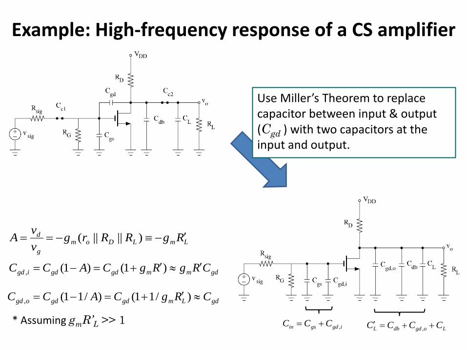
Example: High-frequency response of a CS amplifier
Use Miller’s Theorem to replace capacitor between input & output (Cgd ) with two capacitors at the input and output.
gdmmgdgdigd CRgRgCACC ′≈′+=−= )1()1(,
gdLmgdgdogd CRgCACC ≈′+=−= )/11()/11(,
LmLDomg
d RgRRrgvvA ′−≡−== )||||(
* Assuming gmR’L >> 1igdgsin CCC ,+=
LogddbL CCCC ++=′ ,

Example: High-frequency response of a CS amplifier
1. Consider Cin :
∞
)||( 21
1sigGin
p RRCf
π=
2. Find resistance between Capacitor terminals
Terminals of Cin

Example: High-frequency response of a CS amplifier
1. Consider C’L :
)||||( 21
2LDoL
p RRrCf
′=
π
2. Find resistance between Capacitor terminals
Terminals of C’L

High-frequency response of a CS amplifier
21
21
/1/1/1
)||||1(
)||||( 21/ ),||( 21/
)||||(
ppH
LdbgdL
LDomgdgsin
LDoLpsigGinp
LDomsigG
GM
fffCCCC
RRrgCCCRRrCfRRCf
RRrgRR
RA
+=
++=′
++=
′==
+−=
ππ

Miller’s Theorem vs Miller’s Approximation For Miller Theorem to work, ratio of V2/V1 (amplifier gain) should be
independent of feedback impedance Z.
This was correct for OpAmp example where the gain of the chip, A0 , remains constant when Rf is attached (output resistance of the chip is small).
However, the capacitor that connect the input and output changes the frequency response of the amplifier (i.e., its gain) and so we cannot “strictly” apply Miller’s Theorem.
In our analysis, we used mid-band gain of the transistor and ignored changes in the frequency response due to the feedback capacitor. This is called “Miller’s Approximation.”
Miller’s Approximation only gives “approximate” values of the poles and the higher cut-off frequency.
More importantly, Miller’s Approximation “misses” the zero introduced by the feedback resistor (which can cause “unstable” operation).

Example: High-frequency response of a CG amplifier
o Cdb is ignored in the above. Including body effect, one sees Cdbactually appears between drain and ground (parallel to CL in the above circuit) and is “absorbed” in CL.
o Note that Cgd is also between the drain and the ground and is in parallel to CL.
)( dbLgdL CCCC ++=′

om
LDo
rgRRr ||+
Example: High-frequency response of a CG amplifier
1. Consider Cgs :
]/)||(||[ 21
1omLDosiggs
p rgRRrRCf
+=
π
2. Find resistance between Capacitor terminals
Terminals of Cgs
om
LDo
rgRRr ||+
≈
om
LDo
rgRRr ||+

Example: High-frequency response of a CG amplifier
1. Consider C’L :
)]1(||||[ 21
2sigmoLDL
p RgrRRCf
+′=
π
2. Find resistance between Capacitor terminals
)1( sigmo Rgr +≈
)1( sigmo Rgr +

High-frequency response of a CG amplifier
21
2
1
/1/1/1
)(
)]1(||||[ 2/1
, )||( 2/1/)||(
)||||(
ppH
dbLgdL
sigmoLDLp
isiggsp
omLDoi
LDomsigi
iM
fffCCCC
RgrRRCfRRCf
rgRRrR
RRrgRR
RA
+=
++=′
+′=
=+=
++=
π
π