Frequency Response of Two Stage Rc Coupled Amplifier
38
RC COUPLED AMPLIFIERS
-
Upload
ayesha-gupta -
Category
Documents
-
view
104 -
download
9
description
ppt
Transcript of Frequency Response of Two Stage Rc Coupled Amplifier

RC COUPLED AMPLIFIERS

An electronic amplifier (or amp) is an electronic device made up by a combination of diodes, capacitors, resistors and transistors that increases the power of a signal fed into it.
The power of the signal is amplified by taking energy from a power supply and controlling the output to match the input signal shape but with a larger amplitude.
Thus, an amplifier modulates the output of the power supply.
Amplifier
A common Emitter BJT amplifier

CIRCUIT DESCRIPTION: Resistor and Capacitor are coupled
together in this amplifier. The main purpose of this circuit is
pre-amplification. The CE transistor acts in the active
region. The resistors R1 and R2 are biasing
resistors. Rc is the collector resistor and Re is
the emitter resistor.
RC Coupled Amplifier
Common Emitter RC coupled amplifier

CAPACITORS:
◦ Cin (Capacitor to the Input): The capacitor is used to filter the DC component so as to prevent the alteration of biasing conditions of the transistor and hence reduce the performance.
◦ Cout (Capacitor to the Output): This capacitor is the output DC decoupling capacitor. It prevents any DC voltage from entering into the succeeding stage from the present stage. If this capacitor is not used the output of the amplifier will be clamped by the DC level present at the transistors collector.
◦ Ce (Emitter by-pass Capacitor): When there is no input only the quiescent current set by the biasing resistors R1 and R2 flows through Re. This current is a direct current (a few mA) and Ce does nothing. When input signal is applied, the transistor amplifies it and as a result a corresponding alternating current flows through the Re. The job of Ce is to bypass this alternating component of the emitter current. If Ce is not there , the entire emitter current will flow through Re and that causes a large voltage drop across it. This voltage drop gets added to the Vbe of the transistor and the bias settings will be altered. It is just like giving a heavy negative feedback and so it drastically reduces the gain.

RESISTORS:
The biasing resistors provide the transistor Q1 s base with the necessary bias ′voltage to drive it into the active region. The region of operation where the transistor is completely switched off ( an open switch) is called CUT OFF REGION and the region of operation where the transistor is completely switched on ( a closed switch) is called SATURATION REGION. The region in between cut-off and saturation is called active region. For a transistor amplifier to function properly, it should operate in the active region.
Vce

Values of Rc and Re are so selected that 50% of Vcc gets dropped across the collector & emitter of the transistor.
◦ Rc (Collector resistor) : The value of Re or the collector resistor is selected to be 40% of Vcc. This is done to ensure that the operating point is positioned at the centre of the load line.
◦ Re (Emitter resistor) : The value of Re or the emitter resistor is selected to be 10% of Vcc. This is done to take care that the operating point is positioned at the center of the load line. A higher voltage drop across Re will reduce the output voltage swing and so it is a common practice to keep the voltage drop across Re = 10%Vcc .

INPUT OUTPUT IMPEDENCE OF 2-STAGE RC COUPLED AMPLIFIER
7

CH 11 Frequency Response8
Input Capacitance of Emitter/Source Follower
Lm
GSGDin Rg
CCCCC
1
//
Or

CH 11 Frequency Response9
Example: Source Follower Input Capacitance
1211
1 ||1
1GS
OOmGDin C
rrgCC

CH 11 Frequency Response10
Output Impedance of Emitter Follower
1
sCr
RrsCrR
I
V SS
X
X

CH 11 Frequency Response11
Output Impedance of Source Follower
mGS
GSS
X
X
gsC
sCR
I
V
1

CH 11 Frequency Response12
Active Inductor
The plot above shows the output impedance of emitter and source followers. Since a follower’s primary duty is to lower the driving impedance (RS>1/gm), the “active inductor” characteristic on the right is usually observed.
CH 11 Frequency Response13
Example: Output Impedance
33
321 1||
mGS
GSOO
X
X
gsC
sCrr
I
V
Or

FREQUENCY RESPONSE OF a TWO STAGE RC COUPLED AMPLIFIER

As the gain provided by a single stage amplifier is usually not sufficient to drive the load, so to achieve extra gain multi-stage amplifier are used. In multi-stage amplifiers output of one stage is coupled to the input of the next stage. The coupling of one stage to another is done with the help of some coupling devices. If it is coupled by RC then the amplifier is called RC-coupled amplifier.

OPERATION When ac signal is applied to the base
of the first transistor , it appears in the amplified form across its collector load Rc. the amplified signal developed across Rc is given to base of next stage through coupling capacitor Cc. the second stage does further amplification of the signal. In this way , the cascaded(one after another) stages amplify the signal and the overall gain is considerably increased

FREQUENCY RESPONSE Frequency response of an amplifier is defined as the
variation of gain with respective frequency. The gain of the amplifier increases as the frequency increases from zero till it becomes maximum at lower cut-off frequency and remains constant till higher cut-off frequency and then it falls again as the frequency increases.
AT LOW FREQUENCIES At low frequencies the reactance of coupling capacitor
Cc is quite high and hence very small part of signal will pass from one stage to the next stage. Moreover, Ce cannot shunt the emitter resistance Re effectively because of its large reactance at low frequencies. These two factors cause a falling of voltage gain at low frequencies.
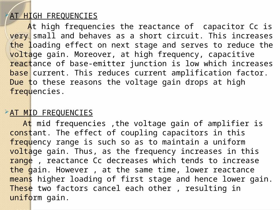
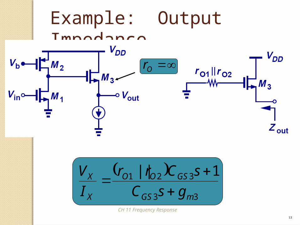
AT HIGH FREQUENCIES At high frequencies the reactance of capacitor Cc is very
small and behaves as a short circuit. This increases the loading effect on next stage and serves to reduce the voltage gain. Moreover, at high frequency, capacitive reactance of base-emitter junction is low which increases base current. This reduces current amplification factor. Due to these reasons the voltage gain drops at high frequencies.
AT MID FREQUENCIES At mid frequencies ,the voltage gain of amplifier is
constant. The effect of coupling capacitors in this frequency range is such so as to maintain a uniform voltage gain. Thus, as the frequency increases in this range , reactance Cc decreases which tends to increase the gain. However , at the same time, lower reactance means higher loading of first stage and hence lower gain. These two factors cancel each other , resulting in uniform gain.
FREQUENCY RESPONSE CURVE

Diode clipper circuits

Contents
This presentation explains the working of different diode clipper circuits like Positive and Negative Diode Clippers, Biased Clipper circuit, and Combinational Clipper Circuit with the help of circuit diagrams and waveforms.

introductionThe basic components required for a clipping
circuit are – an ideal diode and a resistor.In order to fix the clipping level to the
desired amount, a dc battery must also be included.
When the diode is forward biased, it acts as a closed switch, and when it is reverse biased, it acts as an open switch.
Different levels of clipping can be obtained by varying the amount of voltage of the battery and also interchanging the positions of the diode and resistor.

Classification: There are two general categories of
clippers: series and parallel (or shunt). The series configuration is defined as one where diode is in series with the load, while the shunt clipper has the diode in a branch parallel to the load.
Depending on the features of the diode, the positive or negative region of the input signal is “clipped” off and accordingly the diode clippers may be positive or negative clippers.

Positive Diode ClipperIn a positive clipper, the positive half
cycles of the input voltage will be removed.
POSITIVE SERIES CLIPPER: the diode is kept in series with the load.

E(i)
E(o)=0 V
• During the positive half cycle of the input waveform, the diode ‘D’ is reverse biased, which maintains the output voltage at 0 Volts. Thus causes the positive half cycle to be clipped off.

During the negative half cycle of the input, the diode is forward biased and so the negative half cycle appears across the output.

• POSITIVE SHUNT CLIPPER: the diode is kept in parallel with the load.• During the positive half cycle, the diode ‘D’ is forward biased and the diode acts as a closed switch. This causes the diode to conduct heavily. This causes the voltage drop across the diode or across the load resistance RL to be zero. Thus output voltage during the positive half cycles is zero, as shown in the output waveform.

• During the negative half cycles of the input signal voltage, the diode D is reverse biased and behaves as an open switch. Consequently the entire input voltage appears across the diode or across the load resistance RL if R is much smaller than RL

Negative Diode ClipperThe negative clipping circuit is almost
same as the positive clipping circuit, with only one difference. If the diode is reconnected with reversed polarity, the circuits will become for a negative series clipper and negative shunt clipper respectively. The negative series and negative shunt clippers are shown:


In all the above discussions, the diode is considered to be ideal one. In a practical diode, the breakdown voltage will exist (0.7 V for silicon and 0.3 V for Germanium). When this is taken into account, the output wave forms for positive and negative clippers will be of the shape shown in the figure below.

Biased Negative Clipper A biased clipper comes in handy when a small portion
of positive or negative half cycles of the signal voltage is to be removed. When a small portion of the negative half cycle is to be removed, it is called a biased negative clipper.
In a biased clipper, when the input signal voltage is positive, the diode ‘D’ is reverse-biased. This causes it to act as an open-switch. Thus the entire positive half cycle appears across the load.
When the input signal voltage is negative but does not exceed battery the voltage ‘V’, the diode ‘D’ remains reverse-biased and most of the input voltage appears across the output.
When during the negative half cycle of input signal, the signal voltage becomes more than the battery voltage V, the diode D is forward biased and so conducts heavily.

• The output voltage is equal to ‘- V’ and stays at ‘- V’ as long as the magnitude of the input signal voltage is greater than the magnitude of the battery voltage, ‘V’. Thus a biased negative clipper removes input voltage when the input signal voltage becomes greater than the battery voltage.
E(i)= Vmax E(o) = Vmax
E(i)= -Vmax
E(o
) = -V
max

E(o) = -VE(i) = -Vmax
Vmax > V

Biased Positive ClipperClipping can be changed by reversing
the battery and diode connections

Combination clipper
When a portion of both positive and negative of each half cycle of the input voltage is to be clipped (or removed), combination clipper is employed.

Drawbacks In series clippers, when the diode is in ‘OFF’
position, there will be no transmission of input signal to output. But in case of high frequency signals transmission occurs through diode capacitance which is undesirable. This is the drawback of using diode as a series element in such clippers.
In shunt clippers, when diode is in the ‘off condition, transmission of input signal should take place to output. But in case of high frequency input signals, diode capacitance affects the circuit operation adversely and the signal gets attenuated (that is, it passes through diode capacitance to ground).

THANK YOU