
Chapter 23 Transistor Amplifier Low Frequency...
62
_____________________________________________________________________________________________________________________ © 2009 Strangeway, Lokken, Petersen, and Gassert ch. 23 page 1 Chapter 23 Transistor Amplifier Low Frequency Analysis * by Robert Strangeway, Richard Lokken, Owe Petersen, and John Gassert 23.1 Bipolar Junction Transistor Low Frequency Analysis...................................................2 23.1.1 The Need for Low Frequency Response Analysis in BJT CE Amplifiers ..............2 23.1.2 Highpass Effects of the Coupling Capacitors ..........................................................3 23.1.3 Highpass Effect of the Emitter-Bypass Capacitor .................................................11 23.2 Field Effect Transistor Low Frequency Analysis .........................................................17 23.2.1 The Need for Low Frequency Response Analysis in FET CS Amplifiers ............17 23.2.2 Highpass Effects of the Coupling Capacitors ........................................................18 23.2.3 Highpass Effect of the Source-Bypass Capacitor ..................................................24 23.3 Chapter Appendix: Development of the 3 dB Point for Two Closely-Spaced Break Frequencies .......................................................................30 23.4 Class Notes ........................................................................................................................32 23.5 Homework Problems .......................................................................................................59 Note: The order of coverage of sections 23.1 and 23.2, and the corresponding sub-sections of class notes within section 23.4, may be swapped—they are independent sections. Pedagogy (for the instructor): DC bias analysis reinforces and extends mastery of Kirchhoff’s laws DC analysis introduces the concept of an electron device that does not have an ohm’s law type of i-v relationship AC midband analysis introduces dependent sources in a two-port “input-output” context AC midband analysis reinforces/extends mastery of two-port circuit analysis that was begun with first-order filters and in previous electronics courses Frequency response analysis reinforces/extends mastery of transfer functions and break frequencies that was begun with first-order filters * This chapter may be copied and distributed during the 2008-9 academic year to students in the Electrical/Electronics Technology and Engineering Technology programs at College of Lake County, Fox Valley Technical College, Gateway Technical College, Madison Area Technical College, Milwaukee Area Technical College, Milwaukee School of Engineering, Northeast Wisconsin Technical College, Waukesha County Technical College, and Western Technical College, all in the states of Wisconsin or Illinois. Any other reproduction or distribution is prohibited without the express written consent of the first or the second named authors.
Transcript of Chapter 23 Transistor Amplifier Low Frequency...

_____________________________________________________________________________________________________________________
© 2009 Strangeway, Lokken, Petersen, and Gassert ch. 23 page 1
Chapter 23 Transistor Amplifier Low Frequency Analysis*
by Robert Strangeway, Richard Lokken, Owe Petersen, and John Gassert 23.1 Bipolar Junction Transistor Low Frequency Analysis...................................................2
23.1.1 The Need for Low Frequency Response Analysis in BJT CE Amplifiers ..............2
23.1.2 Highpass Effects of the Coupling Capacitors ..........................................................3
23.1.3 Highpass Effect of the Emitter-Bypass Capacitor .................................................11
23.2 Field Effect Transistor Low Frequency Analysis .........................................................17
23.2.1 The Need for Low Frequency Response Analysis in FET CS Amplifiers ............17
23.2.2 Highpass Effects of the Coupling Capacitors ........................................................18
23.2.3 Highpass Effect of the Source-Bypass Capacitor ..................................................24
23.3 Chapter Appendix: Development of the 3 dB Point for Two Closely-Spaced
Break Frequencies .......................................................................30
23.4 Class Notes ........................................................................................................................32
23.5 Homework Problems .......................................................................................................59 Note: The order of coverage of sections 23.1 and 23.2, and the corresponding sub-sections of class notes within section 23.4, may be swapped—they are independent sections. Pedagogy (for the instructor):
DC bias analysis reinforces and extends mastery of Kirchhoff’s laws
DC analysis introduces the concept of an electron device that does not have an ohm’s law type of i-v relationship
AC midband analysis introduces dependent sources in a two-port “input-output” context
AC midband analysis reinforces/extends mastery of two-port circuit analysis that was begun with first-order filters and in previous electronics courses
Frequency response analysis reinforces/extends mastery of transfer functions and break frequencies that was begun with first-order filters
* This chapter may be copied and distributed during the 2008-9 academic year to students in the Electrical/Electronics Technology and Engineering Technology programs at College of Lake County, Fox Valley Technical College, Gateway Technical College, Madison Area Technical College, Milwaukee Area Technical College, Milwaukee School of Engineering, Northeast Wisconsin Technical College, Waukesha County Technical College, and Western Technical College, all in the states of Wisconsin or Illinois. Any other reproduction or distribution is prohibited without the express written consent of the first or the second named authors.
_____________________________________________________________________________________________________________________
© 2009 Strangeway, Lokken, Petersen, and Gassert ch. 23 page 2
Outcomes: As a result of studying this chapter and working the homework problems, the student should be able to:
Explain each step in the development of the transfer functions and the break frequencies that are utilized to determine the low frequency response of a CE/CS transistor amplifier.
Select and utilize the proper results for the determination of the low frequency response of a CE/CS transistor amplifier.
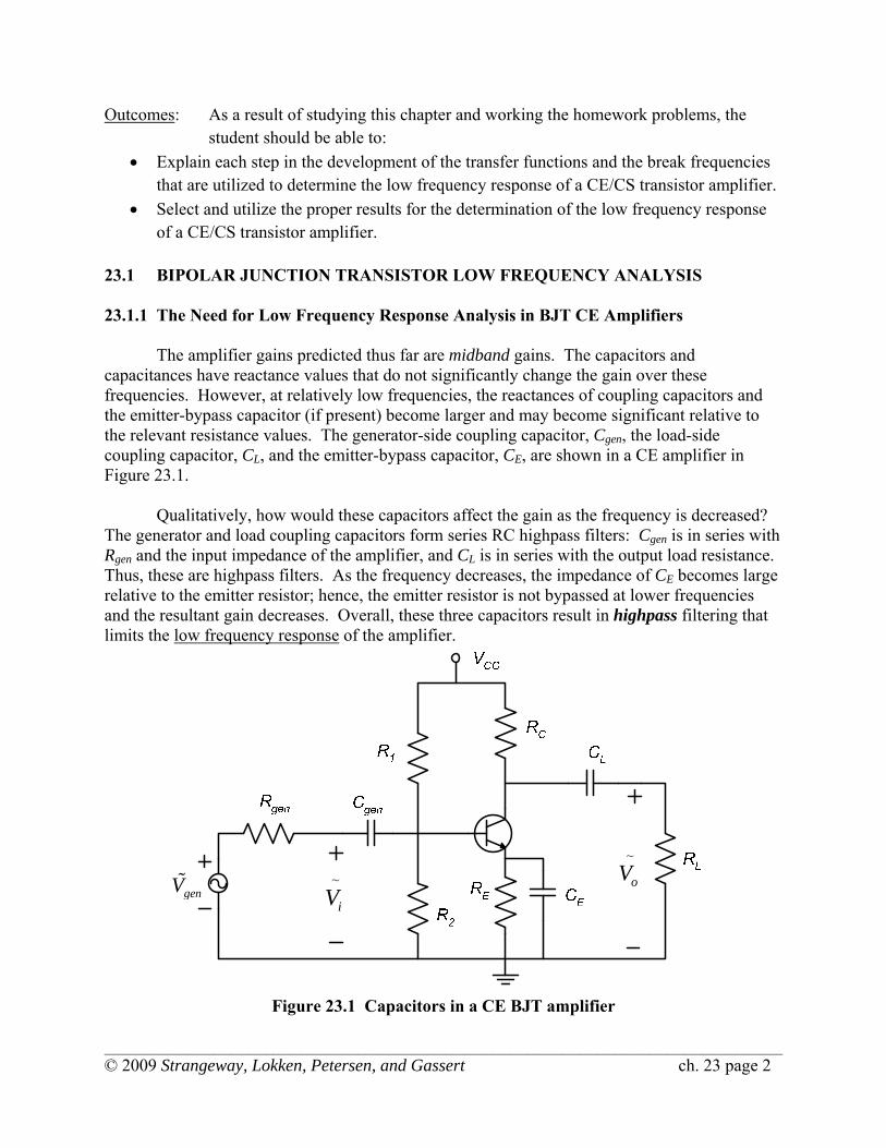
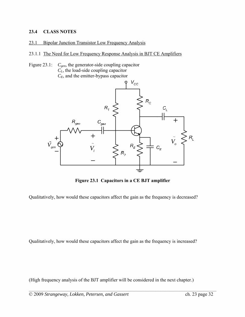
23.1 BIPOLAR JUNCTION TRANSISTOR LOW FREQUENCY ANALYSIS 23.1.1 The Need for Low Frequency Response Analysis in BJT CE Amplifiers The amplifier gains predicted thus far are midband gains. The capacitors and capacitances have reactance values that do not significantly change the gain over these frequencies. However, at relatively low frequencies, the reactances of coupling capacitors and the emitter-bypass capacitor (if present) become larger and may become significant relative to the relevant resistance values. The generator-side coupling capacitor, Cgen, the load-side coupling capacitor, CL, and the emitter-bypass capacitor, CE, are shown in a CE amplifier in Figure 23.1.
Qualitatively, how would these capacitors affect the gain as the frequency is decreased? The generator and load coupling capacitors form series RC highpass filters: Cgen is in series with Rgen and the input impedance of the amplifier, and CL is in series with the output load resistance. Thus, these are highpass filters. As the frequency decreases, the impedance of CE becomes large relative to the emitter resistor; hence, the emitter resistor is not bypassed at lower frequencies and the resultant gain decreases. Overall, these three capacitors result in highpass filtering that limits the low frequency response of the amplifier.
genV ~
iV
~
oV
Figure 23.1 Capacitors in a CE BJT amplifier

_____________________________________________________________________________________________________________________
© 2009 Strangeway, Lokken, Petersen, and Gassert ch. 23 page 3
At high frequencies, the coupling and emitter bypass capacitors have reactance values that are much smaller than the resistance levels and hence, are insignificant. These frequencies are in the passband of the corresponding highpass filters. However, there are other capacitances that become significant at higher frequencies. The effects of these capacitances on the high frequency response of a transistor amplifier will be examined in the next chapter.
How does one approach the analysis of an amplifier at very low frequencies, that is, below the midband frequency range? Fortunately, you already have the tools: frequency response (transfer function) and Bode plot analysis. The overall strategy is:
1) identify the equivalent RC networks formed by the capacitances and resistances in the circuit,
2) determine the transfer function of each RC network, as is done in Bode plot analysis, and 3) modify the midband gain frequency response using the break frequencies and filtering
type (highpass in the low frequency analysis).
There is a hidden assumption in the strategy above: it is assumed that each frequency roll-off effect is independent of the others, that is, that they do not interact. This is not technically true, but usually is “true enough” to give good frequency response predictions. If more exacting predictions are required, one can simulate using the more complicated transistor models that are contained in software packages. Again, the purpose of manual circuit analysis (analysis by hand calculations) is to form starting points for designs and to make reasonable but not exact predictions. The low frequency response of a BJT CE amplifier is examined in this section. The low frequency analysis of an FET CS amplifier is examined in section 23.3. The high frequency responses will be examined in chapter 24. Review transfer function and Bode plot analysis techniques as needed in order to understand the application of the techniques to determine the low frequency response of these amplifiers. 23.1.2 Highpass Effects of the Coupling Capacitors The highpass effects of the coupling capacitors are considered first. The AC model of the BJT with the coupling capacitances is shown in Figure 23.2. The emitter resistance is assumed to be bypassed per the assumption of “non-interacting” capacitances (the effect of CE will be analyzed after the coupling capacitances analysis). The “generator” is the circuit that drives the input of the amplifier. Often, it is the previous stage in the circuit. The load resistance is often either the next stage in the circuit or the device or component that is driven by the amplifier stage. The series Rgen – Cgen – Ri circuit forms a highpass filter, as does the series Ro – CL – RL circuit. Note that Ri is the midband input impedance (resistance) of the BJT amplifier and Ro is the midband output impedance. Also note that even though Rgen is not part of the amplifier, it cannot be ignored because it will affect the value of the break frequency on the generator side.

_____________________________________________________________________________________________________________________
© 2009 Strangeway, Lokken, Petersen, and Gassert ch. 23 page 4
iVgenV
bI
c bI I
oV
Figure 23.2 BJT amplifier model with coupling capacitances
Determine the transfer function. Note how the generator is incorporated into the analysis:
geno o
i i gen
VV VH j
V V V
(23.1)
A crucial step is now performed: the generator resistance-input resistance voltage divider is defined to be at midband (Cgen is effectively a short). The reason for this step is to incorporate
the effects of the generator in the frequency response via o
gen
V
V
while maintaining the transfer
function as o
i
V
V
because these variables define the actual input and the actual output of the
amplifier stage. Thus, the generator resistance-input resistance voltage divider at midband is:
gen i gen gen ii
gen i i i
V R V R RV
R R V R
(23.2)
where i B eR R r . Substitute Eq. (23.2) into Eq. (23.1):
gen gen io o o
i i gen i gen
V R RV V VH j
V V V R V
(23.3)
Use the current divider rule to determine the load current from bI . Multiply by the
load resistance to obtain the output voltage:
1
Co L L b L
C LL
RV I R I R
R R +j C
(23.4)

_____________________________________________________________________________________________________________________
© 2009 Strangeway, Lokken, Petersen, and Gassert ch. 23 page 5
Determine bI from genV by Ohm’s law and the current divider rule:
1
genB Bb gen
B e B egen i
gen
VR RI I
R + r R + rR + R j C
(23.5)
Insert Equation (23.5) into (23.4) and this result into (23.3):
1 1
gen CBo L
B egen i C L
gen L
V RRV R
R + rR + R R R +j C j C
(23.6)
1 1gen C LB
B egen i C L
gen Lgen i
i gen
V R RRR + rR + R R R +
j C j CR RH j
R V
(23.7)
Substitute B eB e
B e
R rR r
R r
for iR in the first factor and simplify:
11 1
gen i C LB
B e B egen i C L
gen LB e
R R R RRH j
R r R + rR + R R R +j C j CR r
(23.8)
11 1
gen i C L
egen i C L
gen L
R R R RH j
r R R R R j C j C
(23.9)
Clear compound fractions:
11 1
gen i gen C L L
e gen Lgen i C L
gen L
R R j C R R j CH j
r j C j CR R R R j C j C
(23.10)
1
1 1gen i gen C L L
e gen i gen C L L
j R R C j R R CH j
r j R R C j R R C
(23.11)

_____________________________________________________________________________________________________________________
© 2009 Strangeway, Lokken, Petersen, and Gassert ch. 23 page 6
The next step is taken in order to simplify the final results of this analysis (trust us!). Factor out
the constant C L
C L
R R
R R
from the numerator of the last factor in order to make the break
frequencies of the numerator and denominator equal:
1 1
gen i gen C L LC L
gen i gen e C L C L L
j R R C j R R CR RH j
j R R C r R R j R R C
(23.12)
Recall the midband gain of the BJT CE amplifier:
C Lb
C Lo C Lv
i b e e C L
R RI
R RV R RA
V I r r R R
(23.13)
1 1gen i gen C L L
vgen i gen C L L
j R R C j R R CH j A
j R R C j R R C
(23.14)
The real parts of the complex numbers are already equal to one. Thus proceed to the next step of
b
j
form:
1 1
1 11 1
gen i gen C L Lv
C L Lgen i gen
j j
R R C R R CH j A
j j
R R CR R C
(23.15)
1 1
bg bLv
bg bL
j j
H j Aj j
(23.16)
where 1 1
and bg bLC L Lgen i gen R R CR R C
are the break frequencies of the highpass
transfer function factors. Note how the generator resistance affects the generator-side break frequency, as does the load resistance on the load-side break frequency. Thus, the entire amplifier transfer function including the effects of the generator and load coupling capacitors is

_____________________________________________________________________________________________________________________
© 2009 Strangeway, Lokken, Petersen, and Gassert ch. 23 page 7
( ) ( )og v L
i
VH j H j A H j
V
(23.17)
1 1
1 1midband1 1 loaded
voltagehighpass highpass gain
gen i gen C L L
v
C L Lgen i gen
Lg
j j
R R C R R CH j A
j j
R R CR R C
H jH j
(23.18)
Thus, the approach to analyze the highpass filtering of the low frequency response of a BJT CE amplifier due to the coupling capacitors is to determine the midband loaded amplifier gain. Then determine the transfer functions of the generator-side and load-side highpass filters:
1
, where 1
bgg bg
gen i gen
bg
j
H jR R Cj
(23.19)
1
, where 1
bLL bL
C L L
bL
j
H jR R Cj
(23.20)
The total amplifier transfer function then is:
( ) ( )og v L
i
VH j H j A H j
V
(23.21)
Thus, the amplifier low frequency response due to the coupling capacitors is obtained by modifying the midband loaded voltage gain with the highpass responses of the generator and load coupling capacitances (via the break frequencies). This realization is important because one can straightforwardly determine the highpass transfer functions of the RC sections on the input and output of the amplifier circuit and, consequently, the low frequency response of the BJT CE amplifier due to the coupling capacitors. This approach is illustrated in Example 23.1.1.

_____________________________________________________________________________________________________________________
© 2009 Strangeway, Lokken, Petersen, and Gassert ch. 23 page 8
Example 23.1.1 Determine the midband and low frequency response for the BJT amplifier shown in Figure 23.3. Consider only the coupling capacitors in the low frequency response (assume the emitter resistor is bypassed).
VCC = +15 V
Cgen
R1RC
CL = 10 μF
RER2
CE
Rgen
RL
genV ~
iV
~
oV200 Ω 10 μF
50μF
1200 Ω
3300 Ω
20 kΩ
2 kΩ120Ω
Figure 23.3 Amplifier for Examples 23.1.1 and 2
Strategy: Determine bias current IE re = 0.026/IE Build the midband amplifier model Determine Av Build the coupling capacitors low frequency amplifier model Determine the high pass break frequencies Sketch and label the midband and low frequency magnitude Bode Plot.
Solution:
Determine the bias conditions, IE , and re
2
1 2
15 20001.3636 V
20k 2000CC
Th
V RV
R R
1 2
1 2
20k 20001.818 k
20k 2000Th
R RR
R R

_____________________________________________________________________________________________________________________
© 2009 Strangeway, Lokken, Petersen, and Gassert ch. 23 page 9
KVL: 1 0
E
Th B Th BE B E
I
V I R V I R
1.3636 0.737.837 A
1 1818 131 120Th BE
BTh E
V VI
R R
1 131 37.837 A 4.9567 mAE BI I
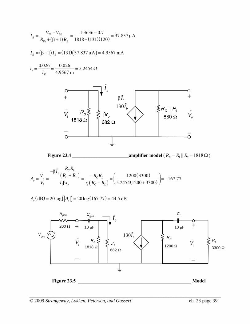
0.026 0.026
5.24544.9567 me
E
rI
Build the midband amplifier model (Figure 23.4); 1 2|| 1818BR R R
~
oV~
iV
bI
130 bIbI
Figure 23.4 Midband amplifier model Determine Av
1200 3300167.77
5.2454 1200 3300
dB 20log 20log 167.77 44.5 dB
C Lb
C Lo C Lv
i b e e C L
v v
R RI
R RV R RA
V I r r R R
A A
Build the coupling capacitor low frequency model (Figure 23.5)

_____________________________________________________________________________________________________________________
© 2009 Strangeway, Lokken, Petersen, and Gassert ch. 23 page 10
RB
CLCgen
~
oV~
iV
Rgen
genVRLre
RC
bI
130 bI200 Ω
1200 Ω 3300 Ω1818 Ω682 Ω
10 μF10 μF
Figure 23.5 Coupling Capacitors Low Frequency Model
Determine the highpass break frequencies
The input of the amplifier is a Rgen-Cgen-Ri highpass filter with 496i e BR r R .
1 1
, 144 rad/s , 23 Hz200 496 101
bgg bg bg
gen i gen
bg
j
H j fR R Cj
The output of the amplifier is a RC-CL-RL highpass filter :
1 1
, 22 rad/s , 3.5 Hz1200 3300 101
bLL bL bL
C L L
bL
j
H j fR R Cj
The total amplifier transfer function then is:
( ) ( )og v L
i
VH j H j A H j
V
23 3.5, 44.5 dB, and 1 1
23 3.5
g v L
f fj j
H j A H jf f
j j
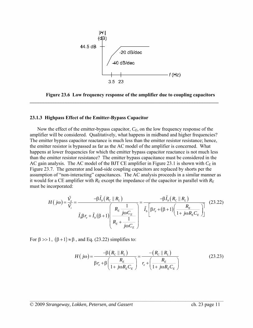
The 23 Hz highpass break frequency dominates the low frequency response (Figure 23.6)
_____________________________________________________________________________________________________________________
© 2009 Strangeway, Lokken, Petersen, and Gassert ch. 23 page 11
Figure 23.6 Low frequency response of the amplifier due to coupling capacitors ____________________________________________________________________________ 23.1.3 Highpass Effect of the Emitter-Bypass Capacitor
Now the effect of the emitter-bypass capacitor, CE, on the low frequency response of the amplifier will be considered. Qualitatively, what happens in midband and higher frequencies? The emitter bypass capacitor reactance is much less than the emitter resistor resistance; hence, the emitter resistor is bypassed as far as the AC model of the amplifier is concerned. What happens at lower frequencies for which the emitter bypass capacitor reactance is not much less than the emitter resistor resistance? The emitter bypass capacitance must be considered in the AC gain analysis. The AC model of the BJT CE amplifier in Figure 23.1 is shown with CE in Figure 23.7. The generator and load-side coupling capacitors are replaced by shorts per the assumption of “non-interacting” capacitances. The AC analysis proceeds in a similar manner as it would for a CE amplifier with RE except the impedance of the capacitor in parallel with RE must be incorporated:
|| ||
11
111
b C L b C Lo
i EE b e
E E Eb e b
EE
I R R I R RVH j
V RR I rj C j R CI r I
Rj C
(23.22)
For 1, 1 , and Eq. (23.22) simplifies to:
|| ||
1 1
C L C L
E Ee e
E E E E
R R R RH j
R Rr r
j R C j R C
(23.23)

_____________________________________________________________________________________________________________________
© 2009 Strangeway, Lokken, Petersen, and Gassert ch. 23 page 12
genViV oV
bIiI
c bI I
Figure 23.7 AC BJT model with RE and CE Recall from a previous example that the midband un-bypassed amplifier voltage gain is:
||C L
v unbypassede E
R RA
r R
(23.24)
A strategic algebraic manipulation at this point can again simplify the final results of this analysis. Factor out a constant such that the remainder is the bypassed voltage gain:
|| ||c L c Le e
v unbypassed v bypassede E e E e e E
v bypassedA
R R R Rr rA A
r R r R r r R
(23.25)
Similarly, algebraically manipulate Eq. (23.23) to show Av-unbypassed and Av-bypassed :
|| || 11
1 11
C L C L E EE E
E E E e E E Ee
E E
R R R R j R Cj R CH j
R j R C r j R C Rr
j R C
(23.26)
|| 1C L E E
e E e E E
R R j R CH j
r R j r R C
(23.27)

_____________________________________________________________________________________________________________________
© 2009 Strangeway, Lokken, Petersen, and Gassert ch. 23 page 13
11
|| 1 ||
11
E EC L E E C L
e E E e Ee E
e Ee E v unbypassed
e E E
A
j
R CR R j R C R RH j
r R C r Rjr R j
r Rr Rr R C
(23.28)
3 3
4 4
1 1
1 1
o b e bv unbypassed v bypassed
s e E
b b
H jE
j jV r
H j A AV r Rj j
(23.29)
where the break frequencies are:
3
1b
E ER C (23.30)
4
1e Eb
e Ee E EE
e E
r Rr Rr R C
Cr R
(23.31)
and the portion of the transfer function due to the emitter bypass capacitor, EH j , is indicated
in Equation (23.29). Note that ωb3 < ωb4 because the total resistance of is re||RE is less than RE. Thus, the transfer function shows the “flat/increasing/flat” highpass response due to CE , as shown in Figure 23.8. If the gain above ωb4 is equal to the gain with the bypassed emitter resistor, what is the gain below ωb3? It must be the gain without the bypassed emitter resistor! Note that ωb3 often occurs below the break frequencies in the highpass responses due to the coupling capacitors.
no thru e EI Call thru e EI C
Figure 23.8 Frequency response due to CE
_____________________________________________________________________________________________________________________
© 2009 Strangeway, Lokken, Petersen, and Gassert ch. 23 page 14
Thus, the low frequency response must include the midband amplifier gain, the highpass effects due to the coupling capacitors, and the highpass effect due to the emitter-bypass capacitor:
( ) ( )og v bypassed E L
i
VH j H j A H j H j
V (23.32)
where:
1
, where 1
bgg bg
gen i gen
bg
j
H jR R Cj
(23.33)
||c L C L
v bypassede e L L
R R R RA
r r R R
(23.34)
33 4
4
11
, where and 1
e b e EE b b
e E E E e E E
b
jr r R
H jr R R C r R Cj
(23.35)
1
, where 1
bLL bL
C L L
bL
j
H jR R Cj
(23.36)
Thus, the amplifier low frequency response is obtained by modifying the midband loaded voltage gain with the highpass responses of the generator and load coupling capacitors and the highpass response of the emitter-bypass capacitor (via the break frequencies). Again, this realization is important because it makes the determination of the low frequency response of a BJT CE amplifier straightforward. The effect with the highest break frequency dominates the low frequency response of the amplifier. The previous example is now reconsidered in Example 23.1.2 to include the effect of the emitter-bypass capacitor.

_____________________________________________________________________________________________________________________
© 2009 Strangeway, Lokken, Petersen, and Gassert ch. 23 page 15
Example 23.1.2 Determine the low frequency response for the BJT amplifier shown in Figure 23.3 of Example 23.1.1. Include the effect of the emitter-bypass capacitor.
Strategy: Determine bias current IE re = 0.026/IE Build the midband amplifier model Determine Av Build the low frequency amplifier model Determine the high pass break frequencies Sketch and label the midband and low frequency magnitude Bode Plot.
The first four steps and part of the fifth and sixth steps were performed in Example 23.1.1. Build the low frequency model with CE (Figure 23.9).
re
RCRB
RE
RL
Rgen
CE
genViV oV
bIiI
c bI I 200 Ω
50 μF
1818 Ω
120 Ω
1200 Ω
CL
10 μF
Cgen
10μF
3300 Ω
682 Ω 130 bI
Figure 23.9 Low frequency BJT amplifier model The RC circuits on the input and the output were already analyzed in Example 23.1.1. Thus, proceed to the amplifier transfer function analysis with CE (Figure 23.10). Note that the generator and load coupling capacitors have been replaced with shorts.

_____________________________________________________________________________________________________________________
© 2009 Strangeway, Lokken, Petersen, and Gassert ch. 23 page 16
iV oV
bI
130 bI
Figure 23.10 Model for HE(jω) determination
3
4
1
1
e bE
e E
b
jr
H jr R j
3 3
1 1166.7 rad/s , 26.5 Hz
120 50b bE E
fR C
4 4
5.2454 1203979.5 rad/s , 633 Hz
5.2454 120 50e E
b be E E
r Rf
r R C
Note that ωb4 dominates the low frequency response because it has the largest frequency. It is also much larger than ωbg and ωbL. Hence, ωb4 dominates the entire low frequency response of the amplifier. It is shown in Figure 23.11.
Figure 23.11. The low frequency amplifier response for Example 23.1.2

_____________________________________________________________________________________________________________________
© 2009 Strangeway, Lokken, Petersen, and Gassert ch. 23 page 17
23.2 FIELD EFFECT TRANSISTOR LOW FREQUENCY ANALYSIS 23.2.1 The Need for Low Frequency Response Analysis in FET CS Amplifiers The FET amplifier gains predicted thus far are midband gains. The capacitors and capacitances have reactance values that do not significantly change the gain over these frequencies. However, at relatively low frequencies, the reactances of coupling capacitors and the source-bypass capacitor (if present) become larger and may become significant relative to the relevant resistance values. The generator-side coupling capacitor, Cgen , the load-side coupling capacitor, CL, and the source-bypass capacitor, CS , are shown in a CS amplifier in Figure 23.12.
Qualitatively, how would these capacitors affect the gain as the frequency is decreased? The generator and load coupling capacitors form series RC highpass filters: Cgen is in series with Rgen and the input impedance of the amplifier, and CL is in series with the output load resistance. Thus, these are highpass filters. As the frequency decreases, the impedance of CS becomes large relative to the source resistor; hence, the source resistor is not bypassed at lower frequencies and the resultant gain decreases. Overall, these three capacitors result in highpass filtering that limits the lower frequency response of the amplifier.
iVoVgenV
Figure 23.12 Capacitors in a CS FET amplifier
At high frequencies, the coupling and source-bypass capacitors have reactance values that are much smaller than the resistance levels and hence, are insignificant. These frequencies are in the passband of the corresponding highpass filters. However, there are other capacitances that become significant at higher frequencies. The effects of these capacitances on the high frequency response of a transistor amplifier will be examined in the next chapter. How does one approach the analysis of an amplifier at very low frequencies, that is, below of the midband frequency range? Fortunately, you already have the tools: frequency response (transfer function) and Bode plot analysis. The overall strategy is:
_____________________________________________________________________________________________________________________
© 2009 Strangeway, Lokken, Petersen, and Gassert ch. 23 page 18
1) identify the equivalent RC networks formed by the capacitances and resistances in the circuit,
2) determine the transfer function of each RC network, as is done in Bode plot analysis, and 3) modify the midband gain frequency response using the break frequencies and filtering
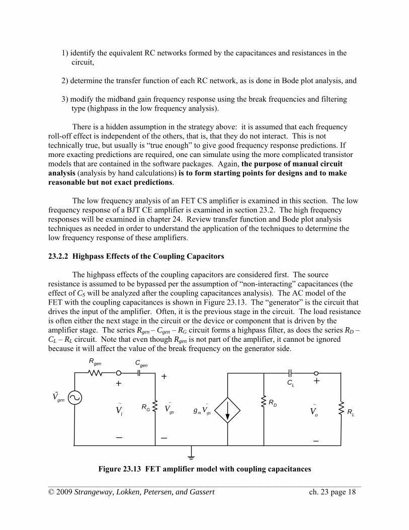
type (highpass in the low frequency analysis). There is a hidden assumption in the strategy above: it is assumed that each frequency roll-off effect is independent of the others, that is, that they do not interact. This is not technically true, but usually is “true enough” to give good frequency response predictions. If more exacting predictions are required, one can simulate using the more complicated transistor models that are contained in the software packages. Again, the purpose of manual circuit analysis (analysis by hand calculations) is to form starting points for designs and to make reasonable but not exact predictions. The low frequency analysis of an FET CS amplifier is examined in this section. The low frequency response of a BJT CE amplifier is examined in section 23.2. The high frequency responses will be examined in chapter 24. Review transfer function and Bode plot analysis techniques as needed in order to understand the application of the techniques to determine the low frequency response of these amplifiers. 23.2.2 Highpass Effects of the Coupling Capacitors The highpass effects of the coupling capacitors are considered first. The source resistance is assumed to be bypassed per the assumption of “non-interacting” capacitances (the effect of CS will be analyzed after the coupling capacitances analysis). The AC model of the FET with the coupling capacitances is shown in Figure 23.13. The “generator” is the circuit that drives the input of the amplifier. Often, it is the previous stage in the circuit. The load resistance is often either the next stage in the circuit or the device or component that is driven by the amplifier stage. The series Rgen – Cgen – RG circuit forms a highpass filter, as does the series RD – CL – RL circuit. Note that even though Rgen is not part of the amplifier, it cannot be ignored because it will affect the value of the break frequency on the generator side.
RG
RD
CL
Cgen
~
oV~
iV~
gsV~
m gsg V
Rgen
genV
RL
Figure 23.13 FET amplifier model with coupling capacitances

_____________________________________________________________________________________________________________________
© 2009 Strangeway, Lokken, Petersen, and Gassert ch. 23 page 19
Determine the transfer function. Note how the generator is incorporated into the analysis:
geno o
i i gen
VV VH j
V V V
(23.37)
The generator resistance-gate resistor voltage divider is defined to be at midband (Cgen is effectively a short):
i
i i
gengeni i
gen gen i
R RVV R
V R R V R
(23.38)
where
i GR R in this FET CS amplifier.
gen gen io o o
i i gen i gen
V R RV V VH j
V V V R V
(23.39)
As with the BJT amplifier analysis, use the current divider rule to determine the load
current from m gsg V . Multiply by the load resistance to obtain the output voltage:
1
Do L L m gs L
D LL
RV I R g V R
R R +j C
(23.40)
Use the voltage divider rule on the input to relate gsV to genV :
1
gen igs
gen igen
V RV
R R +j C
(23.41)
Insert Equation (23.5) into (23.40) and this result into Equation (23.3):
1 1
gen i Do m L
gen i D Lgen L
V R RV g R
R R + R R +j C j C
(23.42)
1 1gen i D L
m
gen i D Lgen Lgen io
i i gen
V R R Rg
R R + R R +j C j CR RV
H jV R V
(23.43)
_____________________________________________________________________________________________________________________
© 2009 Strangeway, Lokken, Petersen, and Gassert ch. 23 page 20
The numerator of the generator-side voltage divider can be multiplied by the gen i
i
R R
R
factor.
Then clear compound fractions:
1 1
gen i gen D L Lm
gen Lgen i D L
gen L
R R j C R R j CH j g
j C j CR R + R R +j C j C
(23.44)
11
gen i gen D L Lm
D L Lgen i gen
j R R C j R R CH j g
j R R C j R R C
(23.45)
In a manner similar to the BJT low frequency amplifier analysis, factor out the constant
D L
D L
R R
R R
from the numerator in order to make the break frequencies of the numerator and
denominator equal:
11
gen i gen D L LD Lm
D L D L Lgen i gen
j R R C j R R CR RH j g
R R j R R C j R R C
(23.46)
11
gen i gen D L LD Lm
D L D L Lgen i gen
j R R C j R R CR RH j g
R R j R R C j R R C
(23.47)
Recall the midband gain of the FET CS amplifier:
D Lv m
D L
R RA g
R R
(23.48)
11
gen i gen D L Lv
D L Lgen i gen
j R R C j R R CH j A
j R R C j R R C
(23.49)
The real part is already equal to one. Thus proceed to the next step of b
j
form:

_____________________________________________________________________________________________________________________
© 2009 Strangeway, Lokken, Petersen, and Gassert ch. 23 page 21
1 1
1 11 1
gen i gen D L Lv
D L Lgen i gen
j j
R R C R R CH j A
j j
R R CR R C
(23.50)
1 1
bg bLv
bg bL
j j
H j Aj j
(23.51)
where 1 1
and bg bLD L Lgen i gen R R CR R C
are the break frequencies of the highpass
transfer functions. Thus, the entire amplifier transfer function including the effects of the generator and load coupling capacitors is:
( ) ( )og v L
i
VH j H j A H j
V
(23.52)
1 1
1 1midband1 1 loaded
voltagehighpass highpass gain
gen i gen D L Lv
D L Lgen i gen
Lg
j j
R R C R R CH j A
j j
R R CR R C
H jH j
(23.53)
Thus, the approach to analyze the highpass filtering at the low frequency response of a FET CS amplifier due to the coupling capacitors is to determine the midband loaded amplifier gain. Then determine the transfer functions of the generator-side and load-side highpass filters:
1
, where 1
bgg bg
gen i gen
bg
j
H jR R Cj
(23.54)

_____________________________________________________________________________________________________________________
© 2009 Strangeway, Lokken, Petersen, and Gassert ch. 23 page 22
1
, where 1
bLL bL
D L L
bL
jH j
R R Cj
(23.55)
The total amplifier transfer function then is:
1 1
bgo bLv
i
bg bL
j jV
H j AV j j
(23.56)
( ) ( )og v L
i
VH j H j A H j
V
(23.57)
Thus, the amplifier low frequency response due to the coupling capacitors is obtained by modifying the midband loaded voltage gain with the highpass responses of the generator and load coupling capacitors (via the break frequencies). Again, this realization is important because it makes the determination of the low frequency response due to the coupling capacitors in a FET CS amplifier straightforward. This approach is illustrated in Example 23.2.1. Example 23.2.1 For the FET common source amplifier shown in Figure 23.14, determine
the midband gain and the low frequency response due to the coupling capacitors, given IDSS = 7 mA and gm = 4 mS. (Note the source bypass capacitor is not considered in the low frequency response yet—it will be considered in the next section and used in the next example.)
iVoV
genV
Figure 23.14 FET amplifier circuit for Examples 23.2.1 and 2

_____________________________________________________________________________________________________________________
© 2009 Strangeway, Lokken, Petersen, and Gassert ch. 23 page 23
Given: The FET circuit in Figure 23.14 IDSS = 7 mA gm = 4 mS
Desired: Av Low frequency response due to the coupling capacitors
Strategy: Determine Av Determine the high pass break frequency for each coupling capacitor Sketch and label the midband and low frequency magnitude Bode plot.
Solution: CS bypasses the source resistor, so the midband voltage gain is determined
in the same manner that it was in Example 23.3.2:
3 1500 2,0004 10 5.33 14.5 dB
1500 2,000o D L
v mi D L
V R RA g
V R R
The AC low frequency model with the coupling capacitors is shown in Figure 23.13. The transfer function due to the midband amplifier gain and the coupling capacitors was determined to be
1 1
bgo bLv
i
bg bL
j jV
H j AV j j
1
where bg
gen i genR R C
and
1
bLD L LR R C
Calculate the generator and load break frequencies:
6
1 10.333 rad/s
100 300k 10 10bg
gen i genR R C
6
1 17.41 rad/s
1500 12k 10 10bL
D L LR R C
Thus the transfer function and low frequency response due to the coupling capacitors is
_____________________________________________________________________________________________________________________
© 2009 Strangeway, Lokken, Petersen, and Gassert ch. 23 page 24
0.333 7.415.331 1 1 1
0.333 7.41
bgo bLv
i
bg bL
j j j jVH j A
V j j j j
This transfer function is plotted in Figure 23.15.
Figure 23.15 Low frequency response due to the coupling capacitors in Example 23.2.1 23.2.3 Highpass Effect of the Source-Bypass Capacitor
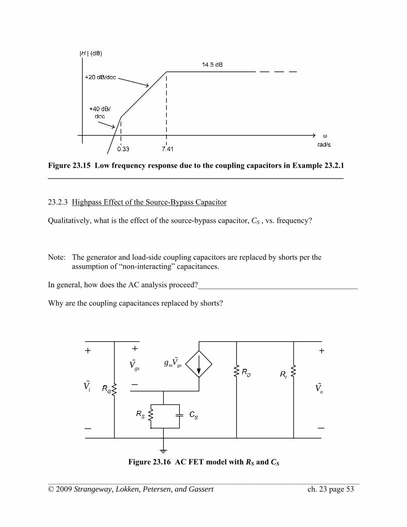
Now the effect of the source-bypass capacitor, CS, on the low frequency response of the amplifier will be considered. Qualitatively, what happens at midband and higher frequencies? The source-bypass capacitor reactance is much less than the source resistor resistance; hence, the source resistor is bypassed as far as the AC model of the amplifier is concerned. What happens at lower frequencies for which the source-bypass capacitor reactance is not much less than the source resistor resistance? Then the source-bypass capacitance must be considered in the AC gain analysis. The AC model of the FET CS amplifier in Figure 23.12 is shown with CS in Figure 23.16. Again, the coupling capacitances are replaced by shorts due to the “non-interacting” capacitors assumption. The AC analysis proceeds in a similar manner as it would for a CS amplifier with RS except the impedance of the capacitor in parallel with RS must be incorporated.

_____________________________________________________________________________________________________________________
© 2009 Strangeway, Lokken, Petersen, and Gassert ch. 23 page 25
iV
gsV
oV
m gsg V
Figure 23.16 AC FET model with RS and CS
Determine the transfer function for the amplifier shown in Figure 23.16. The dependent source current flows through ||D LR R to give the output voltage. The input voltage is the
voltage from the gate to the source plus the voltage across the parallel combination of the source resistor and source-bypass capacitor:
1
1
D Lm gs
D Lo
iS
Sgs m gs
SS
R Rg V
R R VH j
VR
j CV g V
Rj C
(23.58)
The numerator is recognized as the midband voltage gain if RS is bypassed (the same Av that was used in the previous analysis). Clear compound fractions:
1
11
v bypassedo
iS
S Sm
SS
S
AVH j
VR
j C j Cg
j CRj C
(23.59)
1
11
1
v bypassedo S S
Si S Sm
S S
AV j R CH j
RV j R Cg
j R C
(23.60)

_____________________________________________________________________________________________________________________
© 2009 Strangeway, Lokken, Petersen, and Gassert ch. 23 page 26
1 1
1 1S S S S
v bypassed v bypassedS S m S m S S S
j R C j R CH j A A
j R C g R g R j R C
(23.61)
Make the real part equal to one:
1
11
1
v bypassed S S
S Sm S
m S
A j R CH j
R Cg Rj
g R
(23.62)
The constant 1
v bypassed
m S
A
g R
is recognized as the midband amplifier gain if RS is not bypassed.
Proceed to the next step of b
j
form:
11
11
1
v bypassed S S
m S
m S
S S
j
A R CH j
g Rj
g R
R C
(23.63)
3
4
11
1 1
o bv bypassed
i m S
b
jV
H j AV g R j
H jS
(23.64)
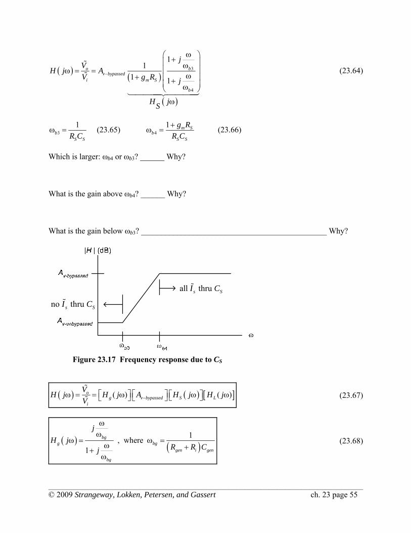
where the break frequencies are:
3
1b
S SR C (23.65)
4
1 m Sb
S S
g R
R C
(23.66)
and the portion of the transfer function due to the source-bypass capacitor, SH j , is indicated
in Eq. (23.64). Note that ωb4 > ωb3 because the numerator of Eq. (23.66) is greater than the numerator of Eq. (23.65), and the denominators are equal. Thus, similar to the transfer function with the emitter bypass capacitor in the BJT CE amplifier, the transfer function shows the “flat/increasing/flat” highpass response due to CS , as shown in Figure 23.17. If the gain above ωb4 is equal to the gain with the bypassed source resistor, what is the gain below ωb3? It must be
_____________________________________________________________________________________________________________________
© 2009 Strangeway, Lokken, Petersen, and Gassert ch. 23 page 27
the gain without the bypassed source resistor! Note that ωb3 often occurs below the break frequencies in the highpass responses due to the coupling capacitors.
b3 b4
no thru s SI C
|H | (dB)
Av-bypassed
all thru s SI C
Av-unbypassed
Figure 23.17 Frequency response due to CS
Thus, the low frequency response must include the midband amplifier gain, the highpass effects due to the coupling capacitors, and the highpass effect due to the source-bypass capacitor:
( ) ( )og v bypassed S L
i
VH j H j A H j H j
V (23.67)
where:
1
, where 1
bgg bg
gen i gen
bg
j
H jR R Cj
(23.68)
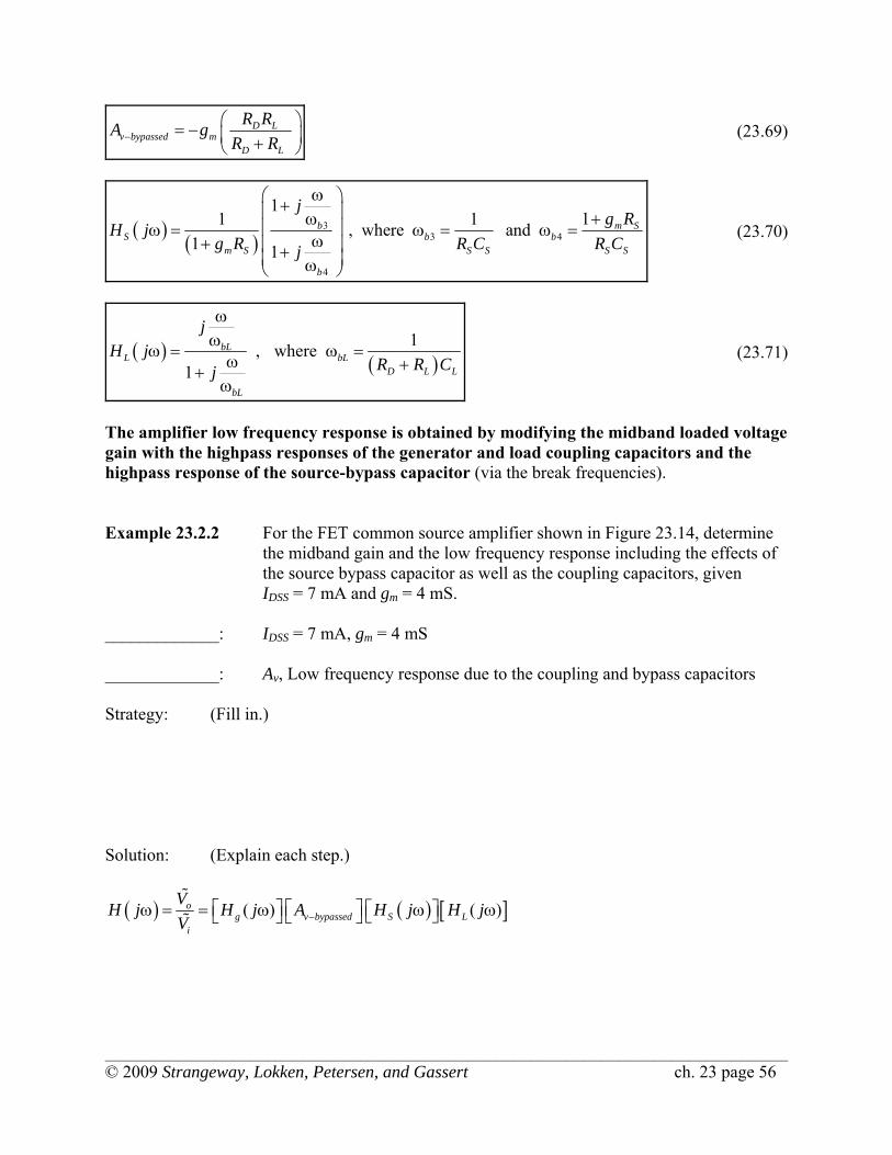
D Lv bypassed m
D L
R RA g
R R
(23.69)
33 4
4
111 1
, where and 1 1
b m SS b b
m S S S S S
b
jg R
H jg R R C R Cj
(23.70)
_____________________________________________________________________________________________________________________
© 2009 Strangeway, Lokken, Petersen, and Gassert ch. 23 page 28
1
, where 1
bLL bL
D L L
bL
jH j
R R Cj
(23.71)
Thus, the amplifier low frequency response is obtained by modifying the midband loaded voltage gain with the highpass responses of the generator and load coupling capacitors and the highpass response of the source-bypass capacitor (via the break frequencies). Again, this realization is important because it makes the determination of the low frequency response in a FET CS amplifier straightforward. The effect with the highest break frequency dominates the low frequency response of the amplifier. The previous example is now reconsidered including the effect of the source-bypass capacitor. Example 23.2.2 For the FET common source amplifier shown in Figure 23.14, determine
the midband gain and the low frequency response including the effects of the source bypass capacitor as well as the coupling capacitors, given IDSS = 7 mA and gm = 4 mS.
Given: The FET circuit in Figure 23.14
IDSS = 7 mA gm = 4 mS
Desired: Av Low frequency response due to the coupling and bypass capacitors
Strategy: Determine Av Determine the high pass break frequencies due to each coupling capacitor
and the source-bypass capacitor Sketch and label the midband and low frequency magnitude Bode plot.
Solution: The overall transfer function for the low frequency response is
( ) ( )og v bypassed S L
i
VH j H j A H j H j
V
3
4
11
11 1 1
bg b bLv bypassed
m S
bg b bL
j j j
H j Ag Rj j j
Av-bypassed, ωbg, and ωbL were determined in Example 23.2.1:

_____________________________________________________________________________________________________________________
© 2009 Strangeway, Lokken, Petersen, and Gassert ch. 23 page 29
3 1500 12,000
4 10 5.33 14.54 dB1500 12,000
o D Lv bypassed m
i D L
V R RA g
V R R
6
1 10.333 rad/s
100 300k 10 10bg
gen i genR R C
6
1 17.41 rad/s
1500 12k 10 10bL
D L LR R C
The break frequencies due to the source-bypass capacitor are
3 6
1 151.3 rad/s
390 50 10b
S SR C
4 6
1 1 0.004 390131.3 rad/s
390 50 10m S
bS S
g R
R C
1 1
0.3906 8.16 dB1 1 0.004 390m Sg R
1
20log 14.54 8.16 dB 6.4 dB1v unbypassed v bypassed
m S
A Ag R
Insert these values into the transfer function and plot the response (Figure 23.18):
3
4
11
11 1 1
bg b bLv bypassed
m S
bg b bL
j j j
H j Ag Rj j j
14.5 dB
2.08 6.4 dB
10.333 51.3 7.415.33 0.3906
1 1 10.333 131.3 7.41
j j jH j
j j j
One notes that the source-bypass capacitor break frequency, 4b , is the largest
highpass frequency in the low frequency response of this FET CS amplifier. Hence, this break frequency sets the low frequency end of the midband amplifier response.

_____________________________________________________________________________________________________________________
© 2009 Strangeway, Lokken, Petersen, and Gassert ch. 23 page 30
Figure 23.18 Low frequency response of the FET CS amplifier in Example 23.2.2 23.3 CHAPTER APPENDIX: Development of the 3 dB Point for Two Closely-Spaced
Break Frequencies
Often the high-end lowpass break frequencies are within one decade of each other in transistor amplifiers. Consider two break frequencies in a lowpass filter that are “closely spaced,” that is, they are less than one decade apart. Both lowpass responses must be considered in the determination of the 3 dB frequency because they are so close together. The magnitude of the transfer function for those terms (a portion of the total transfer function magnitude in dB form) is
2 2
1 2
1 120log 20log
1 1b b
f ff f
(23.72)
The sum of two logarithms is the log of the product:
2 2
1 2
120log
1 1b b
f ff f
(23.73)
Combine the square roots: 2 2
1 2
120log
1 1b b
f ff f
(23.74)
The desired quantity is the frequency at which the previous expression equals -3 dB:

_____________________________________________________________________________________________________________________
© 2009 Strangeway, Lokken, Petersen, and Gassert ch. 23 page 31
2 2
1 2
120log 3 dB
1 1b b
f ff f
(23.75)
Solve for f: 3
20
2 2
1 2
110 0.70795
1 1b b
f ff f
(23.76)
Note that an equation solver (calculator or software) could be utilized at this point to solve for f. Instead, a convenient expression will be developed. Invert and square both side:
2 2
1 2
1 1 1.9953b b
f f
f f
(23.77)
22 2 2
1 2 1 2
1 1.9953b b b b
f f f
f f f f
(23.78)
Multiply through by the common denominator and re-arrange:
24 2 2 21 2 1 20.9953 0b b b bf f f f f f (23.79)
Use the quadratic formula to solve for f 2 :
2 22 2 2 2
1 2 1 2 1 224 0.9953
2b b b b b bf f f f f f
f
(23.80)
2 22 2 2 2 21 2 1 2 1 20.5 0.25 0.9953b b b b b bf f f f f f f (23.81)
Only the plus square root will give a positive value for f 2 (can you explain why?), and only the positive root of f 2 results in a real number. Thus, the frequency at which the lowpass response drops 3 dB when the two break frequencies are within one decade of each other is
2 22 2 2 21 2 1 2 1 20.5 0.25 0.9953b b b b b bf f f f f f f (23.82)
Actually, this equation is also valid for break frequencies spaced farther than one decade, but normal Bode plot approximations are valid in those cases.
_____________________________________________________________________________________________________________________
© 2009 Strangeway, Lokken, Petersen, and Gassert ch. 23 page 32
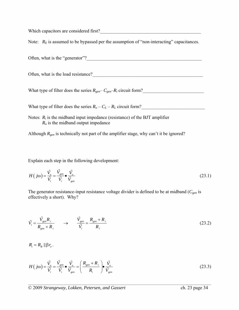
23.4 CLASS NOTES 23.1 Bipolar Junction Transistor Low Frequency Analysis 23.1.1 The Need for Low Frequency Response Analysis in BJT CE Amplifiers Figure 23.1: Cgen, the generator-side coupling capacitor CL, the load-side coupling capacitor CE, and the emitter-bypass capacitor
genV ~
iV
~
oV
Figure 23.1 Capacitors in a CE BJT amplifier
Qualitatively, how would these capacitors affect the gain as the frequency is decreased? Qualitatively, how would these capacitors affect the gain as the frequency is increased? (High frequency analysis of the BJT amplifier will be considered in the next chapter.)

_____________________________________________________________________________________________________________________
© 2009 Strangeway, Lokken, Petersen, and Gassert ch. 23 page 33
What general approach can be taken to analyze an amplifier at very low (or very high) frequencies? Overall strategy:
1) Identify the equivalent RC networks formed by the capacitances and resistances in the circuit,
2) Determine the transfer function of each RC network, as is done in Bode plot analysis, and 3) Modify the midband gain frequency response using the break frequencies and filtering type
(highpass in the low frequency analysis). Assumption: Each frequency roll-off effect is independent of the others (they do not interact).
Technically not true, but usually “true enough” for good frequency response predictions. For more exacting predictions, simulate using the more complicated transistor models
that are contained in software packages. The purpose of manual circuit analysis (analysis by hand calculations) is to form
starting points for designs and to make reasonable but not exact predictions. 23.1.2 Highpass Effects of the Coupling Capacitors What is the circuit in Figure 23.2?____________________________________________
iVgenV
bI
c bI I
oV
Figure 23.2
_____________________________________________________________________________________________________________________
© 2009 Strangeway, Lokken, Petersen, and Gassert ch. 23 page 34
Which capacitors are considered first?___________________________________________ Note: RE is assumed to be bypassed per the assumption of “non-interacting” capacitances. Often, what is the “generator”?_________________________________________________ Often, what is the load resistance?_______________________________________________ What type of filter does the series Rgen– Cgen–Ri circuit form?__________________________ What type of filter does the series Ro – CL – RL circuit form?___________________________ Notes: Ri is the midband input impedance (resistance) of the BJT amplifier Ro is the midband output impedance Although Rgen is technically not part of the amplifier stage, why can’t it be ignored? Explain each step in the following development:
geno o
i i gen
VV VH j
V V V
(23.1)
The generator resistance-input resistance voltage divider is defined to be at midband (Cgen is effectively a short). Why?
gen i gen gen ii
gen i i i
V R V R RV
R R V R
(23.2)
i B eR R r .
gen gen io o o
i i gen i gen
V R RV V VH j
V V V R V
(23.3)

_____________________________________________________________________________________________________________________
© 2009 Strangeway, Lokken, Petersen, and Gassert ch. 23 page 35
1C
o L L b L
C LL
RV I R I R
R R +j C
(23.4)
1genB B
b genB e B e
gen igen
VR RI I
R + r R + rR + R j C
(23.5)
1 1gen CB
o LB e
gen i C Lgen L
V RRV R
R + rR + R R R +j C j C
(23.6)
1 1gen C LB
B egen i C L
gen Lgen i
i gen
V R RRR + rR + R R R +
j C j CR RH j
R V
(23.7)
What does B eB e
B e
R rR r
R r
equal?______________________________________________
11 1
gen i C LB
B e B egen i C L
gen LB e
R R R RRH j
R r R + rR + R R R +j C j CR r
(23.8)
11 1
gen i C L
egen i C L
gen L
R R R RH j
r R R R R j C j C
(23.9)
11 1
gen i gen C L L
e gen Lgen i C L
gen L
R R j C R R j CH j
r j C j CR R R R j C j C
(23.10)

_____________________________________________________________________________________________________________________
© 2009 Strangeway, Lokken, Petersen, and Gassert ch. 23 page 36
1
1 1gen i gen C L L
e gen i gen C L L
j R R C j R R CH j
r j R R C j R R C
(23.11)
The next step simplifies the final results: Factor out the constant C L
C L
R R
R R
from the numerator
of the last factor to make the break frequencies of the numerator and denominator equal. Explain how this was accomplished in the next equation:
1 1
gen i gen C L LC L
gen i gen e C L C L L
j R R C j R R CR RH j
j R R C r R R j R R C
(23.12)
What is
C Lb
C Lo C Lv
i b e e C L
R RI
R RV R RA
V I r r R R
? (23.13)
1 1gen i gen C L L
vgen i gen C L L
j R R C j R R CH j A
j R R C j R R C
(23.14)
Why was the constant C L
C L
R R
R R
factored from the numerator?
1 1
1 11 1
gen i gen C L Lv
C L Lgen i gen
j j
R R C R R CH j A
j j
R R CR R C
(23.15)
1 1
bg bLv
bg bL
j j
H j Aj j
1 1
, bg bLC L Lgen i gen R R CR R C
(23.16)

_____________________________________________________________________________________________________________________
© 2009 Strangeway, Lokken, Petersen, and Gassert ch. 23 page 37
Does the generator resistance affect the generator-side break frequency?__________________ Does the load resistance affect the load-side break frequency?__________________________
( ) ( )og v L
i
VH j H j A H j
V
(23.17)
1 1
1 1midband1 1 loaded
voltagehighpass highpass gain
gen i gen C L L
v
C L Lgen i gen
Lg
j j
R R C R R CH j A
j j
R R CR R C
H jH j
(23.18)
Explain the general approach to analyze the highpass filtering of the low frequency response of a BJT CE amplifier due to the coupling capacitors: Av
1
, where 1
bgg bg
gen i gen
bg
j
H jR R Cj
(23.19)
1
, where 1
bLL bL
C L L
bL
j
H jR R Cj
(23.20)
( ) ( )og v L
i
VH j H j A H j
V
(23.21)
The amplifier low frequency response due to the coupling capacitors is obtained by
modifying the midband loaded voltage gain with the highpass responses of the generator and load coupling capacitances (via the break frequencies).
Where did the break frequencies come from? ________________________________________
_____________________________________________________________________________________________________________________
© 2009 Strangeway, Lokken, Petersen, and Gassert ch. 23 page 38
Example 23.1.1 Determine the midband and low frequency response for the BJT amplifier shown in Figure 23.3. Consider only the coupling capacitors in the low frequency response (assume the emitter resistor is bypassed).
VCC = +15 V
Cgen
R1RC
CL = 10 μF
RER2
CE
Rgen
RL
genV ~
iV
~
oV200 Ω 10 μF
50μF
1200 Ω
3300 Ω
20 kΩ
2 kΩ120Ω
Figure 23.3 Amplifier for Examples 23.1.1 and 2 Strategy: (Fill in.)
Solution: (Explain each step.)
2
1 2
15 20001.3636 V
20k 2000CC
Th
V RV
R R
1 2
1 2
20k 20001.818 k
20k 2000Th
R RR
R R
KVL: 1 0
E
Th B Th BE B E
I
V I R V I R
_____________________________________________________________________________________________________________________
© 2009 Strangeway, Lokken, Petersen, and Gassert ch. 23 page 39
1.3636 0.7
37.837 A1 1818 131 120
Th BEB
Th E
V VI
R R
1 131 37.837 A 4.9567 mAE BI I
0.026 0.026
5.24544.9567 me
E
rI
~
oV~
iV
bI
130 bIbI
Figure 23.4 _______________________amplifier model ( 1 2|| 1818BR R R )
1200 3300167.77
5.2454 1200 3300
dB 20log 20log 167.77 44.5 dB
C Lb
C Lo C Lv
i b e e C L
v v
R RI
R RV R RA
V I r r R R
A A
RB
CLCgen
~
oV~
iV
Rgen
genVRLre
RC
bI
130 bI200 Ω
1200 Ω 3300 Ω1818 Ω682 Ω
10 μF10 μF
Figure 23.5 ______________________________________________ Model
_____________________________________________________________________________________________________________________
© 2009 Strangeway, Lokken, Petersen, and Gassert ch. 23 page 40
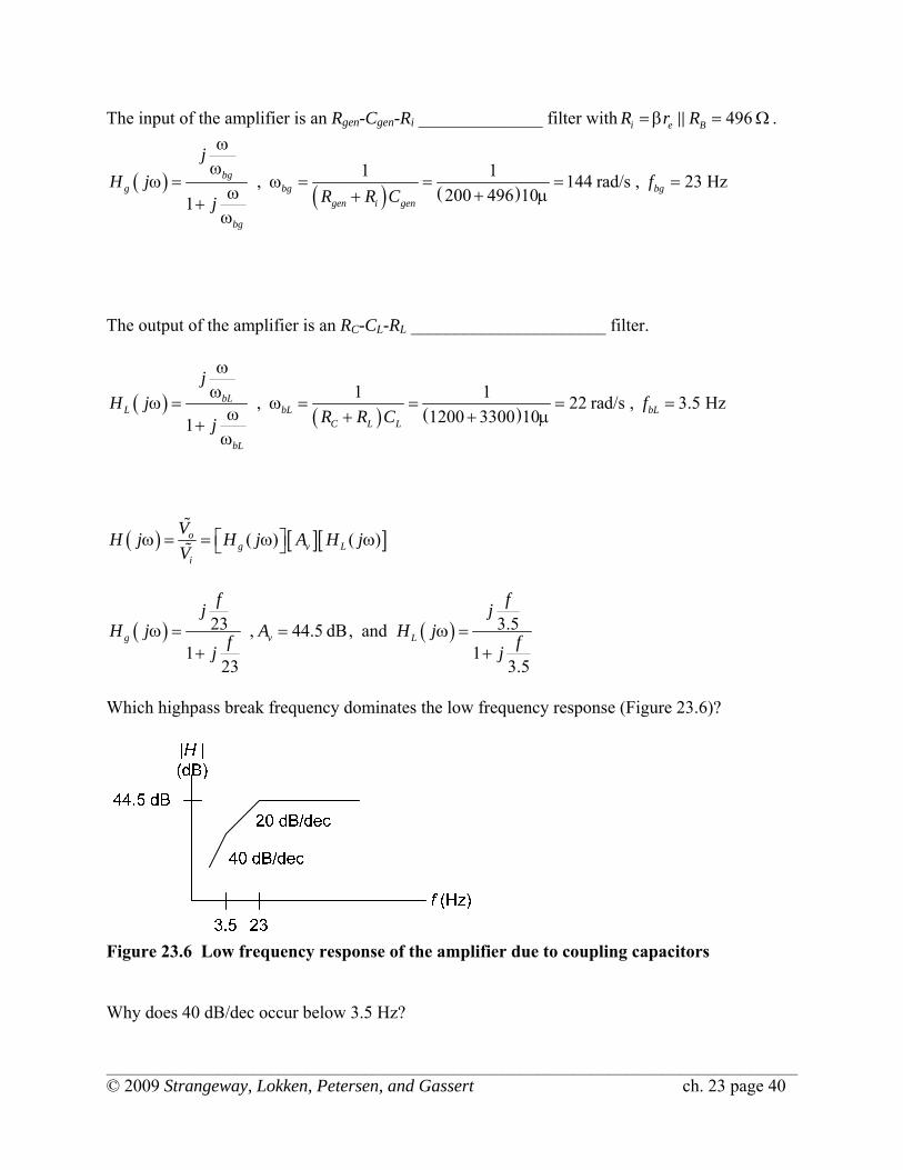
The input of the amplifier is an Rgen-Cgen-Ri ______________ filter with 496i e BR r R .
1 1
, 144 rad/s , 23 Hz200 496 101
bgg bg bg
gen i gen
bg
j
H j fR R Cj
The output of the amplifier is an RC-CL-RL ______________________ filter.
1 1
, 22 rad/s , 3.5 Hz1200 3300 101
bLL bL bL
C L L
bL
j
H j fR R Cj
( ) ( )og v L
i
VH j H j A H j
V
23 3.5, 44.5 dB, and 1 1
23 3.5
g v L
f fj j
H j A H jf f
j j
Which highpass break frequency dominates the low frequency response (Figure 23.6)?
Figure 23.6 Low frequency response of the amplifier due to coupling capacitors Why does 40 dB/dec occur below 3.5 Hz?

_____________________________________________________________________________________________________________________
© 2009 Strangeway, Lokken, Petersen, and Gassert ch. 23 page 41
23.1.3 Highpass Effect of the Emitter-Bypass Capacitor Qualitatively, what is the effect of the emitter-bypass capacitor, CE , vs. frequency? Note: The generator and load-side coupling capacitors are replaced by shorts per the
assumption of “non-interacting” capacitances. In general, how does the AC analysis proceed?________________________________________
genViV oV
bIiI
c bI I
Figure 23.7 AC BJT model with RE and CE
Explain each step:
|| ||
11
111
b C L b C Lo
i EE b e
E E Eb e b
EE
I R R I R RVH j
V RR I rj C j R CI r I
Rj C
(23.22)
|| ||
1 1
C L C L
E Ee e
E E E E
R R R RH j
R Rr r
j R C j R C
(23.23)
||C Lv unbypassed
e E
R RA
r R
(23.24)

_____________________________________________________________________________________________________________________
© 2009 Strangeway, Lokken, Petersen, and Gassert ch. 23 page 42
What algebraic strategy is performed in the next step:
|| ||c L c Le ev unbypassed v bypassed
e E e E e e E
v bypassedA
R R R Rr rA A
r R r R r r R
(23.25)
Similarly, algebraically manipulate Eq. (23.23) to show Av-unbypassed and Av-bypassed :
|| || 11
1 11
C L C L E EE E
E E E e E E Ee
E E
R R R R j R Cj R CH j
R j R C r j R C Rr
j R C
(23.26)
|| 1C L E E
e E e E E
R R j R CH j
r R j r R C
(23.27)
11
|| 1 ||
11
E EC L E E C L
e E E e Ee E
e Ee E v unbypassed
e E E
A
j
R CR R j R C R RH j
r R C r Rjr R j
r Rr Rr R C
(23.28)
3 3
4 4
1 1
1 1
o b e bv unbypassed v bypassed
s e E
b b
H jE
j jV r
H j A AV r Rj j
(23.29)
3
1b
E ER C (23.30) , 4
1e Eb
e Ee E EE
e E
r Rr Rr R C
Cr R
(23.31)
What is EH j ?______________________________________________________________
Which is larger, ωb3 or ωb4? Why? _________________________________________________ What is the gain above ωb4? ______________________________________________________ What is the gain below ωb3? ______________________________________________________

_____________________________________________________________________________________________________________________
© 2009 Strangeway, Lokken, Petersen, and Gassert ch. 23 page 43
Comment: Break frequency ωb3 often (but not always) occurs below the break frequencies in the highpass responses due to the coupling capacitors.
b3 b4
no thru e EI C
|H | (dB)
Av-bypassed
all thru e EI C
Av-unbypassed
Figure 23.8 Frequency response due to CE
( ) ( )og v bypassed E L
i
VH j H j A H j H j
V (23.32)
1
, where 1
bgg bg
gen i gen
bg
j
H jR R Cj
(23.33)
||c L C Lv bypassed
e e C L
R R R RA
r r R R
(23.34)
33 4
4
11
, where and 1
e b e EE b b
e E E E e E E
b
jr r R
H jr R R C r R Cj
(23.35)
1
, where 1
bLL bL
C L L
bL
j
H jR R Cj
(23.36)
The amplifier low frequency response is obtained by modifying the midband loaded voltage gain with the highpass responses of the generator and load coupling capacitors and the highpass response of the emitter-bypass capacitor (via the break frequencies).

_____________________________________________________________________________________________________________________
© 2009 Strangeway, Lokken, Petersen, and Gassert ch. 23 page 44
Example 23.1.2 Determine the low frequency response for the BJT amplifier shown in Figure 23.3 of Example 23.1.1. Include the effect of the emitter-bypass capacitor.
Reminder: Strategy that was executed in Ex. 23.1.1:
Determine bias current IE re = 0.026/IE Build the midband amplifier model Determine Av Build the low frequency amplifier model Determine the high pass break frequencies Sketch/label midband and low freq. magnitude Bode plot.
What additional analysis needs is required to complete the low frequency analysis?
genViV oV
bIiI
c bI I
130 bI
Figure 23.9 Low frequency BJT amplifier model
iV oV
bI
130 bI
Figure 23.10 Model for HE(jω) determination

_____________________________________________________________________________________________________________________
© 2009 Strangeway, Lokken, Petersen, and Gassert ch. 23 page 45
From Ex. 23.1.1:
1200 3300167.77
5.2454 1200 3300
dB 44.5 dB
C Lb
C Lo C Lv
i b e e C L
v
R RI
R RV R RA
V I r r R R
A
1 1
, 144 rad/s , 23 Hz200 496 101
bgg bg bg
gen i gen
bg
j
H j fR R Cj
1 1
, 22 rad/s , 3.5 Hz1200 3300 101
bLL bL bL
C L L
bL
j
H j fR R Cj
Explain the steps in the rest of this example:
3
4
1
1
e bE
e E
b
jr
H jr R j
3 3
1 1166.7 rad/s , 26.5 Hz
120 50b bE E
fR C
4 4
5.2454 1203979.5 rad/s , 633 Hz
5.2454 120 50e E
b be E E
r Rf
r R C
Which break frequency (ωb3 , ωb4 , ωbg or ωbL) dominates the low frequency response? Why?
Figure 23.11. The low frequency amplifier response for Example 23.1.2

_____________________________________________________________________________________________________________________
© 2009 Strangeway, Lokken, Petersen, and Gassert ch. 23 page 46
23.2 Field Effect Transistor Low Frequency Analysis 23.2.1 The Need for Low Frequency Response Analysis in FET CS Amplifiers Which capacitances in Figure 23.12 affect the low frequency response of the FET amplifier? Qualitatively, how would these capacitors affect the gain as the frequency is decreased? Why? Thus, the generator and load coupling capacitors form ___________________________ filters. How does CS affect the amplifier gain as frequency decreases? Why?
iVoVgenV
Figure 23.12 Capacitors in a CS FET amplifier What is the effect of the coupling and source-bypass capacitors at high frequencies? (High frequency analysis of the FET amplifier will be considered in the next chapter.)

_____________________________________________________________________________________________________________________
© 2009 Strangeway, Lokken, Petersen, and Gassert ch. 23 page 47
What general approach can be taken to analyze an amplifier at very low (or very high) frequencies? Overall strategy:
1) Identify the equivalent RC networks formed by the capacitances and resistances in the circuit,
2) Determine the transfer function of each RC network, as is done in Bode plot analysis, and 3) Modify the midband gain frequency response using the break frequencies and filtering type
(highpass in the low frequency analysis). Assumption: Each frequency roll-off effect is independent of the others (they do not interact).
Technically not true, but usually “true enough” for good frequency response predictions. For more exacting predictions, simulate using the more complicated transistor models
that are contained in software packages. The purpose of manual circuit analysis (analysis by hand calculations) is to form
starting points for designs and to make reasonable but not exact predictions. 23.2.2 Highpass Effects of the Coupling Capacitors
RG
RD
CL
Cgen
~
oV~
iV~
gsV~
m gsg V
Rgen
genV
RL
Figure 23.13 FET amplifier model with coupling capacitances
Which capacitors are considered first?___________________________________________ Note: RS is assumed to be bypassed per the assumption of “non-interacting” capacitances.

_____________________________________________________________________________________________________________________
© 2009 Strangeway, Lokken, Petersen, and Gassert ch. 23 page 48
What type of filter does the series Rgen– Cgen–RG circuit form?__________________________ What type of filter does the series RD – CL – RL circuit form?___________________________ Notes: Ri is the midband input impedance (resistance) of the FET amplifier Ro is the midband output impedance Although Rgen is technically not part of the amplifier stage, why can’t it be ignored? Explain each step in the following development:
geno o
i i gen
VV VH j
V V V
(23.37)
i
i i
gengeni i
gen gen i
R RVV R
V R R V R
(23.38)
i GR R
gen gen io o o
i i gen i gen
V R RV V VH j
V V V R V
(23.39)
1D
o L L m gs L
D LL
RV I R g V R
R R +j C
(23.40)
1gen i
gs
gen igen
V RV
R R +j C
(23.41)
1 1gen i D
o m L
gen i D Lgen L
V R RV g R
R R + R R +j C j C
(23.42)

_____________________________________________________________________________________________________________________
© 2009 Strangeway, Lokken, Petersen, and Gassert ch. 23 page 49
1 1gen i D L
m
gen i D Lgen Lgen io
i i gen
V R R Rg
R R + R R +j C j CR RV
H jV R V
(23.43)
1 1
gen i gen D L Lm
gen Lgen i D L
gen L
R R j C R R j CH j g
j C j CR R + R R +j C j C
(23.44)
11
gen i gen D L Lm
D L Lgen i gen
j R R C j R R CH j g
j R R C j R R C
(23.45)
11
gen i gen D L LD Lm
D L D L Lgen i gen
j R R C j R R CR RH j g
R R j R R C j R R C
(23.46)
11
gen i gen D L LD Lm
D L D L Lgen i gen
j R R C j R R CR RH j g
R R j R R C j R R C
(23.47)
D Lv m
D L
R RA g
R R
(23.48)
11
gen i gen D L Lv
D L Lgen i gen
j R R C j R R CH j A
j R R C j R R C
(23.49)

_____________________________________________________________________________________________________________________
© 2009 Strangeway, Lokken, Petersen, and Gassert ch. 23 page 50
1 1
1 11 1
gen i gen D L Lv
D L Lgen i gen
j j
R R C R R CH j A
j j
R R CR R C
(23.50)
1 1
bg bLv
bg bL
j j
H j Aj j
1 1
, bg bLD L Lgen i gen R R CR R C
(23.51)
( ) ( )og v L
i
VH j H j A H j
V
(23.52)
1 1
1 1midband1 1 loaded
voltagehighpass highpass gain
gen i gen D L Lv
D L Lgen i gen
Lg
j j
R R C R R CH j A
j j
R R CR R C
H jH j
(23.53)
1
, where 1
bgg bg
gen i gen
bg
j
H jR R Cj
(23.54)
1
, where 1
bLL bL
D L L
bL
jH j
R R Cj
(23.55)

_____________________________________________________________________________________________________________________
© 2009 Strangeway, Lokken, Petersen, and Gassert ch. 23 page 51
1 1
bgo bLv
i
bg bL
j jV
H j AV j j
(23.56)
( ) ( )og v L
i
VH j H j A H j
V
(23.57)
The amplifier low frequency response due to the coupling capacitors is obtained by modifying the midband loaded voltage gain with the highpass responses of the generator and load coupling capacitors (via the break frequencies). Example 23.2.1 For the FET common source amplifier shown in Figure 23.14, determine the
midband gain and the low frequency response due to the coupling capacitors, given IDSS = 7 mA and gm = 4 mS. (Assume the source resistor is bypassed.)
iVoV
genV
Figure 23.14 FET amplifier circuit for Example 23.2.1 and 2
__________: IDSS = 7 mA, gm = 4 mS __________: Av, Low frequency response due to the coupling capacitors

_____________________________________________________________________________________________________________________
© 2009 Strangeway, Lokken, Petersen, and Gassert ch. 23 page 52
Strategy: (Fill in.) Solution: (Explain each step.)
3 1500 2,0004 10 5.33 14.5 dB
1500 2,000o D L
v mi D L
V R RA g
V R R
1 1
bgo bLv
i
bg bL
j jV
H j AV j j
1
where bg
gen i genR R C
and
1
bLD L LR R C
6
1 10.333 rad/s
100 300k 10 10bg
gen i genR R C
6
1 17.41 rad/s
1500 12k 10 10bL
D L LR R C
0.333 7.415.331 1 1 1
0.333 7.41
bgo bLv
i
bg bL
j j j jVH j A
V j j j j
Which highpass frequency dominates the low frequency response of this FET amplifier? Why?
_____________________________________________________________________________________________________________________
© 2009 Strangeway, Lokken, Petersen, and Gassert ch. 23 page 53
Figure 23.15 Low frequency response due to the coupling capacitors in Example 23.2.1 __________________________________________________________________________ 23.2.3 Highpass Effect of the Source-Bypass Capacitor Qualitatively, what is the effect of the source-bypass capacitor, CS , vs. frequency? Note: The generator and load-side coupling capacitors are replaced by shorts per the
assumption of “non-interacting” capacitances. In general, how does the AC analysis proceed?________________________________________ Why are the coupling capacitances replaced by shorts?
iV
gsV
oV
m gsg V
Figure 23.16 AC FET model with RS and CS

_____________________________________________________________________________________________________________________
© 2009 Strangeway, Lokken, Petersen, and Gassert ch. 23 page 54
1
1
D Lm gs
D Lo
iS
Sgs m gs
SS
R Rg V
R R VH j
VR
j CV g V
Rj C
(23.58)
1
11
v bypassedo
iS
S Sm
SS
S
AVH j
VR
j C j Cg
j CRj C
(23.59)
1
11
1
v bypassedo S S
Si S Sm
S S
AV j R CH j
RV j R Cg
j R C
(23.60)
1 1
1 1S S S S
v bypassed v bypassedS S m S m S S S
j R C j R CH j A A
j R C g R g R j R C
(23.61)
1
11
1
v bypassed S S
S Sm S
m S
A j R CH j
R Cg Rj
g R
(23.62)
The constant 1
v bypassed
m S
A
g R
is recognized as ____________________________________________
11
11
1
v bypassed S S
m S
m S
S S
j
A R CH j
g Rj
g R
R C
(23.63)
_____________________________________________________________________________________________________________________
© 2009 Strangeway, Lokken, Petersen, and Gassert ch. 23 page 55
3
4
11
1 1
o bv bypassed
i m S
b
jV
H j AV g R j
H jS
(23.64)
3
1b
S SR C (23.65) 4
1 m Sb
S S
g R
R C
(23.66)
Which is larger: ωb4 or ωb3? ______ Why? What is the gain above ωb4? ______ Why? What is the gain below ωb3? ______________________________________________ Why?
no thru s SI Call thru s SI C
Figure 23.17 Frequency response due to CS
( ) ( )og v bypassed S L
i
VH j H j A H j H j
V (23.67)
1
, where 1
bgg bg
gen i gen
bg
j
H jR R Cj
(23.68)
_____________________________________________________________________________________________________________________
© 2009 Strangeway, Lokken, Petersen, and Gassert ch. 23 page 56
D Lv bypassed m
D L
R RA g
R R
(23.69)
33 4
4
111 1
, where and 1 1
b m SS b b
m S S S S S
b
jg R
H jg R R C R Cj
(23.70)
1
, where 1
bLL bL
D L L
bL
jH j
R R Cj
(23.71)
The amplifier low frequency response is obtained by modifying the midband loaded voltage gain with the highpass responses of the generator and load coupling capacitors and the highpass response of the source-bypass capacitor (via the break frequencies). Example 23.2.2 For the FET common source amplifier shown in Figure 23.14, determine
the midband gain and the low frequency response including the effects of the source bypass capacitor as well as the coupling capacitors, given IDSS = 7 mA and gm = 4 mS.
_____________: IDSS = 7 mA, gm = 4 mS _____________: Av, Low frequency response due to the coupling and bypass capacitors Strategy: (Fill in.)
Solution: (Explain each step.)
( ) ( )og v bypassed S L
i
VH j H j A H j H j
V

_____________________________________________________________________________________________________________________
© 2009 Strangeway, Lokken, Petersen, and Gassert ch. 23 page 57
3
4
11
11 1 1
bg b bLv bypassed
m S
bg b bL
j j j
H j Ag Rj j j
Av-bypassed, ωbg, and ωbL were determined in Example 23.2.1:
3 1500 12,0004 10 5.33 14.54 dB
1500 12,000o D L
v bypassed mi D L
V R RA g
V R R
6
1 10.333 rad/s
100 300k 10 10bg
gen i genR R C
6
1 17.41 rad/s
1500 12k 10 10bL
D L LR R C
Calculate the remaining pertinent quantities for this example and insert into H(jω). (The results are on the next page.)

_____________________________________________________________________________________________________________________
© 2009 Strangeway, Lokken, Petersen, and Gassert ch. 23 page 58
Results: 3 51.3 rad/sb , 4 131.3 rad/sb ,
10.3906 8.16 dB
1 m Sg R
1
20log 6.4 dB1v unbypassed v bypassed
m S
A Ag R
3
4
11
11 1 1
bg b bLv bypassed
m S
bg b bL
j j j
H j Ag Rj j j
14.5 dB
2.08 6.4 dB
10.333 51.3 7.415.33 0.3906
1 1 10.333 131.3 7.41
j j jH j
j j j
Figure 23.18 Low frequency response of the FET CS amplifier in Example 23.2.2 Which break frequency dominates the low frequency response of this amplifier? _____________ Why?
_____________________________________________________________________________________________________________________
© 2009 Strangeway, Lokken, Petersen, and Gassert ch. 23 page 59
23.5 HOMEWORK PROBLEMS 1. How are coupling and bypass capacitors modeled within midband in a small signal
analysis of a transistor amplifier? 2. How are coupling and bypass capacitors modeled above midband in a small signal
analysis of a transistor amplifier? 3. How are coupling and bypass capacitors modeled below midband in a small signal
analysis of a transistor amplifier? 4. What is the criterion to determine which break frequency dominates the low frequency
response of a transistor amplifier? 5. What key assumption was made about the roll-off effect of each break frequency?

_____________________________________________________________________________________________________________________
© 2009 Strangeway, Lokken, Petersen, and Gassert ch. 23 page 60
6. For the circuit in Figure 23.6, a) determine the break frequencies and sketch/label the magnitude Bode plot showing the
dominant highpass break frequency (note: the bias solution was determined in Problem 6 of Ch. 21, and the midband analysis was performed in Problem 6 of Ch. 22),
b) simulate with a 2N3904 BJT to determine both the magnitude and phase low and
midband frequency responses, c) compare the results to parts a) and b), especially any differences (explain why), d) remove CE and re-simulate, and e) compare the results of parts b) and d) to determine the effects of CE on the frequency
response. Include a comparison of the practical bandwidth over which the phase is relatively constant.
NOTE: The phase response in MultiSIM often “jumps” between -180° and +180°. This
action is due to the method that the phase response is calculated (and is common in many programs and instrument readouts). Actually, the phase is continuing below -180° and is not to be construed as a sudden phase change.
R1 = 6.8 kΩ R2 = 1 kΩ RC = 560 Ω RE = 120 Ω RL = 820 Ω Cgen = 1 μF CL = 1 μF CE = 22 μF VCC = 9 V Rgen = 50 Ω β = 165
VCC
Cgen
R1
RC
CL
RER2CE
Rgen
RL
genV ~
iV
~
oV
Figure P23.6 BJT amplifier circuit for Problem 6
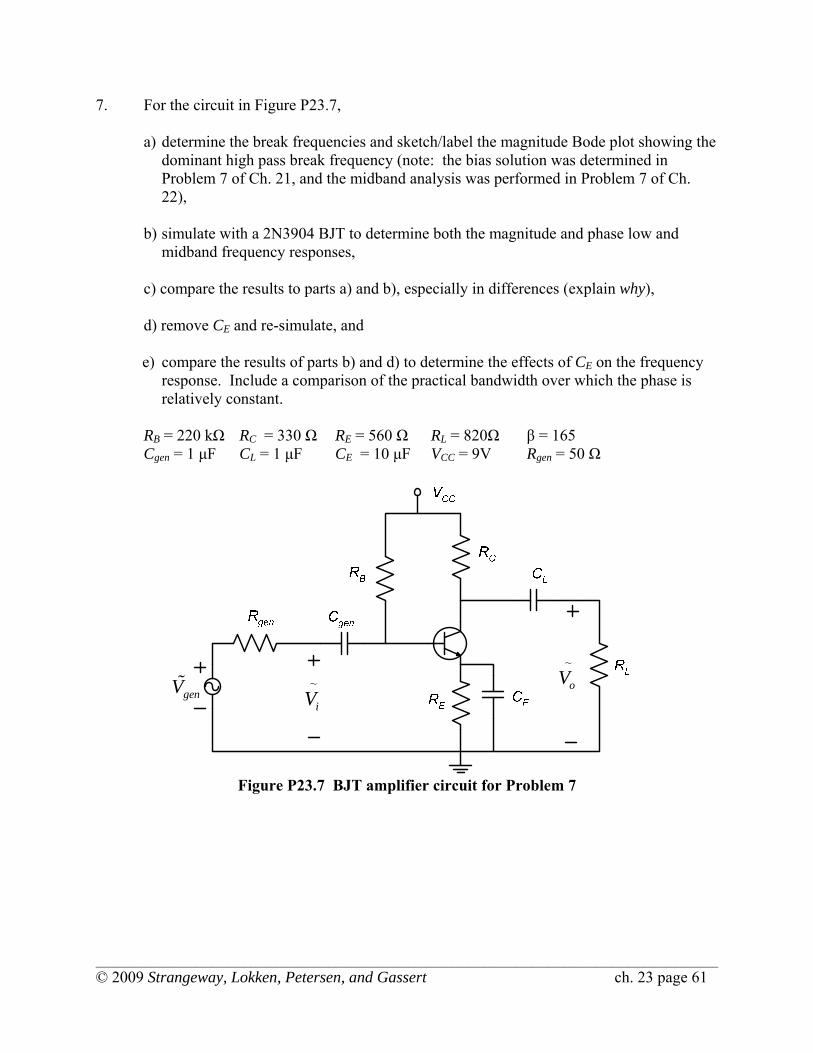
_____________________________________________________________________________________________________________________
© 2009 Strangeway, Lokken, Petersen, and Gassert ch. 23 page 61
7. For the circuit in Figure P23.7,
a) determine the break frequencies and sketch/label the magnitude Bode plot showing the dominant high pass break frequency (note: the bias solution was determined in Problem 7 of Ch. 21, and the midband analysis was performed in Problem 7 of Ch. 22),
b) simulate with a 2N3904 BJT to determine both the magnitude and phase low and
midband frequency responses, c) compare the results to parts a) and b), especially in differences (explain why), d) remove CE and re-simulate, and e) compare the results of parts b) and d) to determine the effects of CE on the frequency
response. Include a comparison of the practical bandwidth over which the phase is relatively constant.
RB = 220 kΩ RC = 330 Ω RE = 560 Ω RL = 820Ω β = 165 Cgen = 1 μF CL = 1 μF CE = 10 μF VCC = 9V Rgen = 50 Ω
genV ~
iV
~
oV
Figure P23.7 BJT amplifier circuit for Problem 7

_____________________________________________________________________________________________________________________
© 2009 Strangeway, Lokken, Petersen, and Gassert ch. 23 page 62
8. For the circuit in Figure P23.8,
a) determine the break frequencies and sketch/label the magnitude Bode plot showing the dominant high pass break frequency (note: the bias solution was determined in Problem 8 of Ch. 21, and the midband analysis was performed in Problem 8 of Ch. 22),
b) simulate with a 2N4393 JFET to determine both the magnitude and phase low and
midband frequency responses, c) compare the results to parts a) and b), especially any differences (explain why), d) remove CS and re-simulate, and e) compare the results of parts b) and d) to determine the effects of CS on the frequency
response. RG = 510 kΩ RD = 1 kΩ RS = 560 Ω RL = 1 kΩ IDSS = 20 mA
VDD = 9V Rgen = 50 Ω VGS(off) = -1.5 V Cgen = 1 μF CL = 1 μF CS = 10 μF
iVoVgenV
Figure P23.8 FET amplifier circuit for Problem 8
9. How are the low-frequency response analyses of BJT and FET amplifiers similar?
Different?


![POWER AMPLIFIER KAC-7204 - ePanorama · KAC-7204 POWER AMPLIFIER Stereo/Bridgeable Power Amplifier BASS BOOST LEVEL[dB] LPF FREQUENCY[Hz] HPF FREQUENCY[Hz] INPUT SENSITIVITY[V] [MIN]](https://static.fdocuments.net/doc/165x107/5f0714757e708231d41b33c5/power-amplifier-kac-7204-epanorama-kac-7204-power-amplifier-stereobridgeable.jpg)