
A CMOS power amplifier in nanometer technology for ...
108
This document is downloaded from DR‑NTU (https://dr.ntu.edu.sg) Nanyang Technological University, Singapore. A CMOS power amplifier in nanometer technology for portable applications Xiao, Fei 2016 https://hdl.handle.net/10356/69246 https://doi.org/10.32657/10356/69246 Downloaded on 18 Mar 2022 15:02:38 SGT
Transcript of A CMOS power amplifier in nanometer technology for ...

This document is downloaded from DR‑NTU (https://dr.ntu.edu.sg)Nanyang Technological University, Singapore.
A CMOS power amplifier in nanometer technologyfor portable applications
Xiao, Fei
2016
https://hdl.handle.net/10356/69246
https://doi.org/10.32657/10356/69246
Downloaded on 18 Mar 2022 15:02:38 SGT

A CMOS POWER AMPLIFIER IN NANOMETER
TECHNOLOGY FOR PORTABLE APPLICATIONS
XIAO FEI
SCHOOL OF ELECTRICAL AND ELECTRONIC
ENGINEERING
2016
A CMOS Power Amplifier in Nanometer Technology
for Portable Applications
Xiao Fei
School of Electrical and Electronic Engineering
A thesis submitted to the Nanyang Technological University
in partial fulfilment of the requirement for the degree of
Master of Engineering
2016
i
Acknowledgment
I would like to take this opportunity to express my warm thanks to my supervisor,
Associate Prof Chan Pak Kwong, for his kindly help and patient guidance. He gave
me the valuable instructions and suggestions when doing this project. I leant a lot of
important fundamental design techniques from Prof Chan. Without the patient
guidance from Prof Chan, I would not finish the work in given milestones for review,
design, simulations and measurement.
I am also thankful to the PhD candidates, Mr. Koay Kuan Chuang and Wang Dong,
for introducing a complete integrated design flow and suggesting me when facing
with some difficulties in the chip design and measurement. I would also like to thank
the PhD graduate, Dr Tan Xiao Liang, for teaching me the beauty of IC design and
answering many questions patiently. He also explained to me a lot of technologies
about analog integrated circuit design.
Lastly, I would like to express my thanks to MediaTek, Singapore for providing me
the MEng scholarship and chip fabrication opportunity.

ii
Table of Contents
ACKNOWLEDGMENT .................................................................................................. I
TABLE OF CONTENTS ................................................................................................ II
ABSTRACT .................................................................................................................. IV
LIST OF FIGURES ...................................................................................................... VI
LIST OF TABLES ........................................................................................................ IX
LIST OF GLOSSARY .................................................................................................... X
CHAPTER 1 INTRODUCTION .................................................................................... 1
1.1. Motivations .......................................................................................................... 1
1.2. Objectives ............................................................................................................ 4
1.3. Contributions ....................................................................................................... 5
1.4. Organizations ....................................................................................................... 6
CHAPTER 2 LITERATURE REVIEW ......................................................................... 7
2.1. Introduction.......................................................................................................... 7
2.2. Review of Class-AB Audio Power Amplifier ..................................................... 9
2.2.1. Dhanasekaran’s Circuit [3]........................................................................... 11
2.2.2. Mohan’s Circuit [5] ...................................................................................... 14
2.3. Review of Low Offset Techniques .................................................................... 18
2.3.1. Yu’s Circuit [28] .......................................................................................... 21
2.4. Review of Frequency Compensation Techniques ............................................. 25
CHAPTER 3 ARCHITECTURE AND CIRCUIT DESIGN........................................ 30
3.1. Proposed Digitally-Assisted Offset Calibration Circuit .................................... 30
3.1.1. Architecture of Proposed Digitally-Assisted Low-offset Headphone
Amplifier ................................................................................................................ 30
3.1.2. Transistor Level of Digitally-Assisted Offset Calibration Circuit ............... 34
3.1.2.1. Balanced Offset Compensation Current Injection Circuit ..................... 34
3.1.2.2. Other Circuit Blocks of the Offset Calibration Circuit .......................... 37
3.1.3. Influence of Input-offset, Temperature and Power Transistors Leakage
Current on Quiescent Power Consumption of Headphone Amplifier.................... 42
3.1.4. Advantages of Balanced Low-impedance Node Current Injection Circuit .. 45
3.2. Proposed Frequency Compensation Topology .................................................. 47
3.3. Transistor Level Realization of Headphone Amplifier ..................................... 55

iii
3.3.1. Realization of Input Stage of Headphone Amplifier .................................... 55
3.3.2. Realization of Second Stage of Headphone Amplifier ................................ 57
3.3.3. Realization of Output Stage of Headphone Amplifier ................................. 59
3.3.4. CLM-Reduced Class-AB Bias Generation Circuit ...................................... 60
3.3.5. Bias Generation and Start-up Circuit ........................................................... 68
3.4. Noise Analysis of Proposed Headphone Amplifier ........................................... 71
CHAPTER 4 MEASURED RESULTS AND DISCUSSIONS.................................... 74
4.1. Measured Input-referred Offset and Quiescent Power ...................................... 76
4.2. Measured THD+N and SNR Results ................................................................. 78
4.3. Measured PSRR Results .................................................................................... 80
4.4. Measured Pulse Response.................................................................................. 81
4.5. Performance Comparison .................................................................................. 83
CHAPTER 5 CONCLUSIONS AND FUTURE WORKS ........................................... 85
5.1. Conclusions ....................................................................................................... 85
5.2. Future Work ....................................................................................................... 86
AUTHOR’S PUBLICATION ....................................................................................... 87
REFERENCES ............................................................................................................. 88

iv
Abstract
In recent years, the demand for the battery-powered devices has been increasing
rapidly. At the same time, the requirements for the audio power amplifier (APA) also
extend to hi-fi quality music playback. In order to achieve high run time per charge
for the portable devices, the quiescent power consumption of APA should be made as
low as possible. As such, the quiescent power consumption, harmonic distortion and
dynamic range become the most significant performance parameters in the design of
high-performance headphone amplifiers. Compared to the class-D amplifier, class-
AB amplifier has the key advantages of high PSRR, low THD+N, no switching noise
and no electro-magnetic interference.
In this thesis, a low-quiescent class-AB headphone driver, which is powered by dual
supplies of ±1V, is presented and analyzed. Due to the small resistive load of APA,
the mismatch-induced quiescent current caused by the input-referred offset voltage
becomes a significant effect on the quiescent power consumption. It is evident that
the mismatch-induced quiescent current of APA will be substantially increased with
the increase of amplifier offset. A new balanced offset compensation current
approach is presented. Through the aid of digitally-assisted calibration design, the
input-referred offset can be substantially reduced while avoiding the unnecessary
increase of quiescent power. Since the compensation current is injected into the low
impedance nodes of the front-end gain stage, there is no significant degradation in
terms of DC gain and power supply rejection ratio (PSRR) of the amplifier. This has
demonstrated the robustness of calibration circuit.

v
An improved compensation technique called NMCFNR2, which is the Type-II
implementation of nested Miller compensation with feedforward and nulling resistor
(NMCFNR) amplifier, is proposed. It offers the technical advantages of simplicity as
well as low-quiescent operation. Besides, the modified frequency compensation
permits the APA to drive the worst-case load of 16Ω//2nF whilst sustaining good
stability and offering good and balanced performance metrics.
Together with the channel-length modulation (CLM) reduced class-AB bias
generation circuit dedicated to the push-pull output stage, the auto-calibrated APA
will reduce the input-referred offset of amplifier down to about 85µV while the total
quiescent power is only 0.4mW and the GBW is of about 1.78 MHz. The APA can
deliver a peak power of 35mW (1.5Vpp swing) to the worse case load of (16Ω//2nF)
with -89dB THD+N and 93.5dB SNR. The extensive measurement results have
suggested that the proposed amplifier has achieved the best Figure-of-Merit FOM1=
(Peak load power/Quiescent power) and the best FOM2= [Peak load
power/Quiescent power*(THD+N)%] when compared with other representative
state-of-the-art works.

vi
List of Figures
Figure 1.1 The configuration of headphone amplifier with differential inputs and input-
referred offset in DC-coupled topology. ............................................................................ 2
Figure 2.1 A two-stage class-AB audio power amplifier with folded-cascode input
stage and conventional bias generation circuit. ................................................................. 9
Figure 2.2 Transistor level of the 16Ω driver proposed by Dhanasekaran [3]. ............... 12
Figure 2.3 The circuit concept of the compensation scheme proposed by Dhanasekaran
[3]. .................................................................................................................................... 13
Figure 2.4 Architecture of the three-stage audio power amplifier proposed by Mohan
[5]. .................................................................................................................................... 14
Figure 2.5 Simplified schematic of PMOS input fully differential amplifier
implemented in the second stage proposed by Mohan [5]. .............................................. 15
Figure 2.6 The architecture of a chopped amplifier. ........................................................ 18
Figure 2.7 Concept of offset calibration circuit proposed in [28]. ................................... 20
Figure 2.8 Topology of ping-pong operational amplifier proposed in [28]. .................... 21
Figure 2.9 Offset adjustable two-stage CMOS op-amp with a programmable current
mirror proposed by Yu [28]. ............................................................................................ 23
Figure 2.10 Topology of three-stage NMC amplifier [37]. ............................................. 25
Figure 2.11 Topology of three-stage NMCFNR amplifier [51]. ..................................... 28
Figure 3.1 The headphone amplifier with the proposed digitally-assisted offset
calibration circuit. ............................................................................................................ 31
Figure 3.2 Simulated transient response of the important signals in the offset
calibration system. ........................................................................................................... 33
Figure 3.3 Concept of balanced offset compensation current injected into differential
input stage. ....................................................................................................................... 34
Figure 3.4 Transistor level of four current sources for balanced current injection. ......... 35
Figure 3.5 Power-on reset circuit. .................................................................................... 38
Figure 3.6 Transient response of the power-on reset circuit when the amplifier starts up.
.......................................................................................................................................... 38
Figure 3.7 Zero-crossing detection logic. ........................................................................ 39
Figure 3.8 Transient responses of the signals in zero-crossing detection logic. .............. 40

vii
Figure 3.9 The quiescent power consumption of proposed power amplifier under
different temperature and input-referred offset voltage. .................................................. 43
Figure 3.10 Temperature variation of power transistors leakage current with in
different corners. .............................................................................................................. 44
Figure 3.11 Comparative simulation results of PSRR for the current injection offset
compensation amplifier and the benchmark headphone amplifier: (a) using proposed
balanced low-impedance node injection circuit, (b) using single-ended high-impedance
node injection circuit. ....................................................................................................... 46
Figure 3.12 Topology of proposed three-stage NMCFNR2 amplifier. ........................... 47
Figure 3.13 Simulated open-loop gain and phase with different nulling resistors for (a)
NMCFNR2 amplifier and (b) NMCFNR amplifier. ........................................................ 49
Figure 3.14 Process Monte Carlo histograms for phase and gain margins with the
respective load of 16Ω//0pF and 16Ω//2nF. .................................................................... 52
Figure 3.15 Simulated PM for RL=16Ω, 32Ω and 50Ω when sweeping the CL from 0pF
to 2nF. .............................................................................................................................. 53
Figure 3.16 The approximated headphone impedance model [69]. ................................. 54
Figure 3.17 The simulated open-loop gain and phase for headphone amplifier using the
approximated headphone impedance load model. ........................................................... 54
Figure 3.18 The simplified schematic of the APA with embodiment of proposed
balanced offset compensation circuit and CLM-reduced class-AB bias generation
circuit. .............................................................................................................................. 56
Figure 3.19 Illustration of biasing current flow in one of floating biasing transistors
when the output voltage of APA goes positive. ............................................................... 58
Figure 3.20 CLM-reduced class-AB bias generation circuit. .......................................... 61
Figure 3.21 Monte Carlo simulation results for offset current using the CLM-reduced
bias generation circuit. ..................................................................................................... 62
Figure 3.22 Monte Carlo simulation results for offset current using the conventional
bias generation circuit. ..................................................................................................... 62
Figure 3.23 The schematic of APA with high-voltage CLM-reduced bias generation
circuit in ±1.5V supply. ................................................................................................... 64
Figure 3.24 Monte Carlo simulation for offset current using the high-voltage CLM-
reduced bias generation circuit with ±1.5V supply. ........................................................ 65
viii
Figure 3.25 Monte Carlo simulation for offset current using the conventional high-
voltage bias generation circuit with ±1.5V supply. ......................................................... 66
Figure 3.26 The total quiescent power versus the input offset of amplifier under two
different biasing circuits. ................................................................................................. 66
Figure 3.27 Constant transconductance bias circuit with startup circuit. ........................ 68
Figure 3.28 The temperature variation of DC current for bias circuit. ............................ 69
Figure 3.29 The folded-cascode stage of the proposed headphone amplifier. ................. 71
Figure 3.30 Input-referred noise of amplifier versus the input pair channel length. ....... 73
Figure 4.1 The micrograph of the proposed headphone amplifier in 65-nm CMOS. ...... 74
Figure 4.2 The Cadence layout drawing of the proposed headphone amplifier in UMC
65-nm CMOS. .................................................................................................................. 75
Figure 4.3 Measured input-referred offset of ten chips with/without offset calibration. . 76
Figure 4.4 Measured quiescent power consumption of ten chips with/without offset
calibration. ....................................................................................................................... 77
Figure 4.5 Measured output signal in FFT with the 1.5VPP 1 kHz input sinusoidal wave.
.......................................................................................................................................... 78
Figure 4.6 Measured THD+N versus output amplitude for 1 kHz input signal. ............. 79
Figure 4.7 Measured THD+N versus signal frequency with 1.5VPP input sine-wave
signal. ............................................................................................................................... 79
Figure 4.8 Measured PSRR+ at 217Hz with 700mVPP on the 1V positive supply. ......... 80
Figure 4.9 Measured PSRR- at 217Hz with 700mVPP on the 1V negative supply. ......... 80
Figure 4.10. Measurement result of a rectangular input waveforms of 50kHz and
500mV with the load of 1nF//16Ω. .................................................................................. 81
Figure 4.11 The pulse response of the headphone amplifier with the respective load of
16Ω//8pF, 16Ω//300pF, 16Ω//1nF and 16Ω//2nF. ........................................................... 82

ix
List of Tables
Table 3.1 The Offset-induced Quiescent Power Consumption Study of Headphone
Amplifier .......................................................................................................................... 42
Table 3.2 Comparison of poles and zeros for two frequency compensation techniques . 51
Table 3.3 Comparison of APAs with the conventional biasing circuit and the improved
biasing circuit for the push-pull output stage. .................................................................. 67
Table 4.1 Performance comparison of reported prior-art results. .................................... 84
x
List of Glossary
APA Audio Power Amplifier
CLM Channel Length Modulation
CMFB Common Mode Feedback
COX Gate Oxide Capacitance
DAC Digital to Analog Converter
DFCFC Damping Factor Control Frequency Compensation
FFT Fast Fourier Transform
FOM Figure of Merit
GBW Gain Bandwidth Product
KFn Flicker Noise coefficient for NMOS
KFp Flicker Noise coefficient for PMOS
LDO Low Dropout
LHP Left-Hand Plane
LPF Low Pass Filter
LSB Least Significant Bit
MNMC Multipath Nested Miller Compensation
MSB Most Significant Bit
NMC Nested Miller Compensation
NMCFNR Nested Miller Compensation with Feedforward Stage and Nulling
Resistor
OTA Operational Transconductance Amplifier
PM Phase Margin
PoR Power-on Reset

xi
PSRR Power Supply Rejection Ratio
PTAT Proportional to Absolute Temperature
RHP Right-Hand Plane
SNR Signal-to-Noise Ratio
THD Total Harmonic Distortion
THD+N Total Harmonic Distortion and Noise
UGF Unity Gain Frequency
hi-fi high-fidelity
k Boltzmann Constant
µ Mobility Carrier

1
Chapter 1 Introduction
1.1. Motivations
For the past few years, the development of portable mobile devices has leaded to the
requirement for more features such as low-power consumption and high integration.
With the rapid development of smartphones in recent years, it has demonstrated
sophisticated features. As one of the most important components in headphone, audio
power amplifiers (APA) are widely used in music player, video player and hand-free
calls. Therefore, the high performance audio power amplifiers will be another demand
in research. Total harmonic distortion (THD), signal-to-noise ratio (SNR) and power
supply rejection ratio (PSRR) are the key parameters that qualify the performance
metrics of an audio power amplifier. Meanwhile, the total quiescent power
consumption of amplifier should be minimized for the purpose of extending the service
life of battery [1].
Class-AB power amplifier is one of common architectures which is regularly used in
the design of headphone amplifier [2]–[8]. It has some technical advantages over other
types of power amplifiers. Compared to the switching amplifier (i.e., class-D
amplifier), the linear amplifier can achieve high PSRR, low total harmonic distortion
plus noise (THD+N), no switching noise and no electro-magnetic interference [9]–[11]
whilst featuring with low power attribute. Therefore, the class-AB topology will be
suitable for the low-quiescent high performance headphone amplifier design. In order
to achieve a fully integrated circuit, a DC-coupled topology is applied. The example is
shown in Fig. 1.1.

2
Driver
R1
R2
R3
R4
CL RL
VOUT
VDD
VSS
VOFF
VIN-
VIN+
Figure 1.1 The configuration of headphone amplifier with differential inputs and
input-referred offset in DC-coupled topology.
Although class-AB power amplifiers can achieve high performance with less quiescent
power, there are several factors that may degrade the quiescent power in class-AB
headphone amplifiers.
Firstly, the input-referred offset for a DC-coupled power amplifier will have a
mismatch-induced quiescent current up to hundreds of µA, which is undesirable for a
low-power design. With the continual decrease in device sizes, the input-referred offset
becomes larger due to the random mismatch in the differential input stage. Refer to
Fig. 1.1, in the presence of input-referred offset, the output voltage is obtained as
2 4 2 4
1 3 1 3
1OUT IN IN OFF
R R R RV V V V
R R R R
(1.1)
where the symbols have their usual meanings. When the four resistors are assumed
identical in design, the input offset will be amplified by two times.
Secondly, the continual decrease in device sizes and supply voltage in nanometer
CMOS technologies will cause the decrease of per-stage gain. As a result, multistage
3
amplifier topologies are required to achieve sufficient DC gain and linearity. Since the
headphone amplifiers should be able to drive the cable capacitance with at least few
hundreds of pF or above [12]–[14], the frequency compensation technique must
guarantee the stability of headphone amplifier in the context of low resistive load in
parallel with high capacitive load. Due to this reason, the frequency compensation
becomes crucial because it directly affects the quiescent power of the amplifier for
given bandwidth in design. In addition, since the output stage accounts for the majority
of the quiescent power in the amplifier, the total quiescent power may increase a lot if
the output stage is not well controlled by the bias generation circuit. Several circuit
techniques will be proposed in this project to design a low-quiescent power class-AB
headphone amplifier. They permit the total harmonic distortion better than or at least
comparable to the recently-published works. More importantly, the best Figure-of-
Merit (FOM) pertaining to the ratio of peak load power to quiescent power is obtained.

4
1.2. Objectives
The objectives of this thesis are given as follows:
(i) To investigate a low offset calibration circuit to eliminate the mismatch-
induced current in the headphone amplifier without degrading other
performance metrics;
(ii) To conduct the small-signal analysis of headphone amplifier and devising an
improved frequency compensation to drive hundreds of pF capacitive load with
good power-bandwidth efficiency;
(iii) To exploit an improved class-AB bias generation circuit to control the
quiescent current of the output stage;
(iv) To conduct the measurement of the test chips which are fabricated using UMC
65nm CMOS technology.
5
1.3. Contributions
The main contributions of the research work are summarized as follows:
(i) By proposing a new offset calibration circuit to reduce the input-referred offset
and the mismatch-induced current of headphone amplifier, the input-referred
offset can be less than 85µV whilst the other performance metrics of
headphone amplifier are not degraded.
(ii) By investigating an improved frequency compensation topology applicable for
low-resistive and high-capacitive load driven power amplifier, the
compensation technique permits the headphone amplifier to drive a capacitive
load range of 0-2nF with good power-bandwidth efficiency.
(iii) By designing a low-quiescent power class-AB headphone amplifier with
dedicated class-AB output stage bias generation circuit, the headphone
amplifier consumes lower power than the recently-published state-of-art works
whilst offering good power-bandwidth and comparable performance metrics
such as THD+N, SNR and PSRR.
6
1.4. Organizations
This thesis consists of six chapters as follows.
Chapter one introduces the background and defines the objectives as well as the main
contributions of the thesis.
Chapter two reviews the representative class-AB headphone amplifier circuit, low-
offset design techniques, multistage amplifier frequency compensation techniques and
the recently-published state-of-the-art works. These will serve as the benchmarks for
this project.
Chapter three describes the design procedures and design considerations pertaining to
the proposed headphone amplifier. The working principle of circuit design techniques
are discussed and analysed in details.
Chapter four presents the extensive measurement results and discusses the
performance aspects of the circuit and the performance comparison with the recently-
published state-of-art works, demonstrating the effectiveness of the amplifier.
Chapter five gives the concluding remarks and the recommendations for future
improvements.
7
Chapter 2 Literature Review
The conventional class-AB headphone amplifier design techniques and low-offset
circuit techniques will be reviewed in this chapter. The working principle of the
recently-published works will be studied and discussed. This is then followed by the
discussion of the representative multistage amplifier frequency compensation
topologies.
2.1. Introduction
The audio power amplifier is widely used in our daily life. It is used to amplify the
low-power audio signal which is in the frequency range of 20-20kHz to drive a
loudspeaker. It is widely used in public address systems, home stereo system and
concert sound reinforcement systems. Headphone amplifier is an audio power
amplifier that is usually used in the portable devices. While the requirements for the
headphone amplifier are different from other audio systems, especially the quiescent
power consumption for the portable headphone amplifier should be made preferably
low whenever possible.
For DC-coupled headphone amplifier, the input offset will be amplified. It induces the
offset mismatch-induced current at the output node [15]–[17]. Input offset voltage
becomes a significant problem for headphone amplifier when decreasing the total
quiescent power consumption is one of primary design objectives. This is mainly
because the mismatch-induced quiescent current caused by the input offset voltage
tends to be very high if the offset of amplifier is not effectively nulled. Besides, the use
of small transistor sizes will degrade the offset performance due to the increase of

8
random mismatches as well as the channel length modulation effect in nanometer
CMOS technology. This may not be mitigated by only layout strategies. Therefore, the
offset metric is an important parameter for the headphone amplifier. In order to
achieve high-precision amplifiers, three different offset cancellation techniques can be
implemented. They are chopping technique, auto-zeroing technique and trimming
technique. Chopping and auto-zeroing techniques are common dynamic approaches
that they can effectively reduce the offset of amplifiers. Some exemplary dynamic
offset cancellation circuits have been reported in [18]–[27]. However, the big power
filtering becomes the challenging issue for these techniques to be applied in APA
design. Turning to the trimming technique, it is regarded as a static approach through
which the input offset is usually calibrated before the main circuit start working.
Several offset trimming circuits have been reported in [28]–[36]. This becomes the key
focus of this work.
Consider the frequency compensation techniques for the multistage headphone
amplifiers, they are similar to that of the capacitive driven op-amp. However, the main
issue is that the different types of driven load have caused significant impact on the
effectiveness of frequency compensation. A lot of works [37]–[66] are reported on the
frequency compensation circuit techniques which are used to stabilize the multistage
amplifiers whilst improving the power-bandwidth efficiency. In order to explore the
appropriate frequency compensation techniques for use in the headphone amplifier,
several representative works [37]–[66] will be reviewed in this chapter.

9
2.2. Review of Class-AB Audio Power Amplifier
Class-AB headphone amplifier has been widely implemented in many recently-
published works [2]–[8]. Most of the architectures in these works are largely based on
two-stage or three-stage design.
Vin+Vin-
VDD
VSS
M1 M2
M3 M4
M5 M6
M8
MP
MN
VOUT
I1 I2 I3
MN'
M7'
IB MP'
IB
Differential Input Stage Output StageBias Generation circuit
M8'
M7 Cm
Cm
Figure 2.1 A two-stage class-AB audio power amplifier with folded-cascode input
stage and conventional bias generation circuit.
A high-gain APA topology can be configured as shown in Fig. 2.1, which is a two-
stage design. It features a high gain folded-cascode input stage and an inverting push-
pull output stage. Frequency compensation can be achieved by means of Miller
compensation. Refer to the two-stage amplifier example in Fig. 2.1, the output stage
biasing circuit makes use of conventional bias generation circuit [67] to bias the
NMOS output transistor by two diode-connected transistors having the gate-source
tracking relationship that VGSN' = VGSN and VGSM8' = VGSM8. However, it suffers from the
problem that the drain-source voltage of the replica transistor MN' is different from that
of the output transistor MN. In addition, due to the high-drive requirement, the channel
10
length of output transistor MN is made small, and hence its replica MN' follows the
same for tracking reason. As a consequence, the channel length modulation effect
becomes a serious problem because this leads to the current matching issue between
the bias generation circuit and the output stage. The same goes for PMOS counterpart.
In order to achieve sufficiently high gain, most of audio power amplifiers are three-
stage topology [2]–[7]. It is common to see that the same bias generation circuit of Fig.
2.1 is utilized in [3], [7], [8]. In a general three-stage audio power amplifier, the first
stage is a differential high-gain stage. The output node of the first stage usually defines
the dominant pole of audio power amplifier. The cascode configuration can provide
high DC gain and high input common mode level. To further increase the gain, the
regulated cascode configuration [2] can be applied. Besides, the folded cascode
configuration is commonly used as the front-end stage in other audio power amplifiers
[3], [8]. Regarding the second gain stage, it is usually achieved with the non-inverting
gain topology having the current mirror active load. It stems from that the fact it
permits the ease with the use of Miller frequency compensation for the last inverting
driving stage. Finally, the third gain stage consists of an NMOS and PMOS to form the
push-pull structure to provide sufficient driving current to the resistive load.
Unfortunately, all the reported works [2]–[8] may exhibit high quiescent current in the
topologies. To stabilize a three-stage circuit architecture with minimum quiescent
current, an effective frequency compensation technique is required in the design of
headphone amplifier.
In view of these pitfalls, the bias generation circuit and frequency compensation
technique are needed to be explored.

11
2.2.1. Dhanasekaran’s Circuit [3]
Of the performance metrics for headphone amplifiers, the quiescent power
consumption, THD+N, PSRR and SNR are identified as the important parameters.
Many studies of the class-AB headphone amplifiers are focused on these metrics.
Dhanasekaran presents a class-AB headphone amplifier in 0.13µm technology. It can
drive 1pF to 22nF capacitive load and achieve -84.8dB THD while consuming a power
of 1.2mW [3]. Fig. 2.2 shows the transistor level of Dhanasekaran’s headphone
amplifier circuit which employs a folded-cascode topology as the input differential
stage, a non-inverting second gain stage with current mirror as active load and a push-
pull output stage. For the output stage, the conventional floating bias network for push-
pull output stage is applied.
Dhanasekaran suggests the frequency compensation scheme which can adjust the
damping factor automatically according to the load capacitance. Most of the three-
stage frequency compensation techniques are based on Miller compensation, in which
the value of damping factor determines the stability of the circuit [50]. Since the
damping factor of a nested Miller compensated (NMC) amplifier is inversely
proportional to LC , it can only drive small capacitive load. On the contrary, the
damping factor of a damping factor control frequency compensated (DFCFC)
amplifier is proportional to LC . This means that it is suitable for large capacitive
load. In order to handle wide range of capacitive load, Dhanasekaran presents a three-
stage amplifier with approximately constant damping factor based on DFCFC and
NMC, which is illustrated in Fig. 2.3. Since the damping factor of DFCFC is
proportional to mD LG C , an approximately constant damping factor can be achieved if

12
Vin+Vin-
VDD
VSS
M13
M9 M9
M10 M10
M2
M1
VOUT
LS
LSM14
M12
VB3
VB2
VB1
Rf Rf
M7 M7'
M8RB
CD
M6
M3M4
M5
M1c
M2c
CD2
VDDD
VSSD
CC RC
CC2
VB6
VB4 VB5
CD
RB
VB
VB
Input Stage Non-inverting Gain Stage Output Stage
M12
M11M11
M13
GmD
GmD
Figure 2.2 Transistor level of the 16Ω driver proposed by Dhanasekaran [3].
13
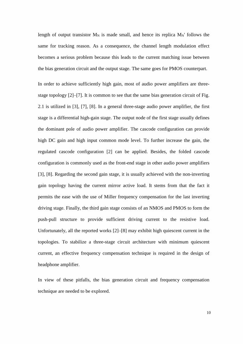
1/GmD can be replaced with a resistor that is proportional toLC . The equivalent
damping resistance RD1 due to CD2 and Gm3 becomes
1
3 2*
LD
m D
CR
G C (2.1)
The total damping resistance of amplifier is given as
1
1||D D
mD
R RG
(2.2)
where GmD is the transconductance of transistor M5 or M6. The resulting damping
resistance is approximately proportional to LC so that the proposed amplifier is able
to drive wide range of capacitive load.
CC
CC2
RC
Gm2 Gm3
VO2VO
CL
CD2CD
GmD
RBVB
Ceq1 Ceq2
1/GmD CL/Gm3CD2
Vi Gm1
Figure 2.3 The circuit concept of the compensation scheme proposed by
Dhanasekaran [3].
14
However, the circuit architecture will consume extra quiescent power consumption by
the active damping stage and the input-referred offset arising from the mismatches in
the amplifier.
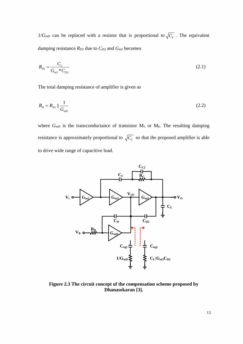
2.2.2. Mohan’s Circuit [5]
The conventional class-AB power amplifier topology shown in Fig. 2.1 is one of the
most popular topologies in the implementation of class-AB headphone amplifier. The
circuit proposed in [5] applies fully differential internal stages to achieve relatively
high output swing and cancel the even-order harmonics. Multiple compensation
networks are adopted to guarantee the stability when driving the capacitive load range
of 10pF ~ 5nF. The peak load power of the reported headphone amplifier delivered to
the 16Ω resistive load is 93.8mW. The peak THD+N is obtained as -77.9dB.
Vin+
Vin-
A1
A2N
A2P
Vo1+
Vo1-
Cc3
Cc3
2Cc3
2Cc3
Cc2
Cc2
-A3P
Rc2
Cc1 Rc1
-A3N
Vout
Vo2N+
Vo2P+
Figure 2.4 Architecture of the three-stage audio power amplifier proposed by
Mohan [5].
15
VB1
VB2
VB3
VB1
VB2
VB3
M6M5
M4M3
M10
M12
M13 M14
M11
M7
M8
M2 M9
M16
M15
M1
R2R2
Vo1-
Vo2P+
VR
VSS
VDD
VC
VB1
VB2M18
M17
MRN
Vo1+
Vo2P-
Cc3 Cc3CS CS
IB
Figure 2.5 Simplified schematic of PMOS input fully differential amplifier
implemented in the second stage proposed by Mohan [5].
Fig. 2.4 shows the architecture of the reported headphone amplifier in [5]. The outputs
of the first fully differential stage are Vo1+ and Vo1-, which have the common mode
voltage of 0V. In the fully differential amplifier shown in Fig. 2.5, the first amplifier
serves as the input differential amplifier whereas the second amplifier provides the
feedback function. There are two fully differential amplifiers implemented in the
second stage, with PMOS input pair as shown in Fig. 2.5 and an NMOS counterpart to
drive the N-type and P-type output transistors in the output stage, respectively. This
architecture can provide same gains and poles frequency at the output nodes of the
second stage. The two resistors R2 and the transistors M9-M14 in the circuit form the
common mode feedback (CMFB) networks. The common mode output voltage of the
fully differential stage is determined by the reference voltage VR in the second
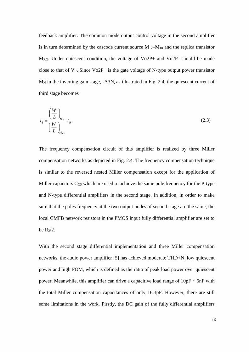
16
feedback amplifier. The common mode output control voltage in the second amplifier
is in turn determined by the cascode current source M17‒M18 and the replica transistor
MRN. Under quiescent condition, the voltage of Vo2P+ and Vo2P- should be made
close to that of VR. Since Vo2P+ is the gate voltage of N-type output power transistor
MN in the inverting gain stage, -A3N, as illustrated in Fig. 2.4, the quiescent current of
third stage becomes
3
N
RN
M
B
M
W
LI I
W
L
(2.3)
The frequency compensation circuit of this amplifier is realized by three Miller
compensation networks as depicted in Fig. 2.4. The frequency compensation technique
is similar to the reversed nested Miller compensation except for the application of
Miller capacitors CC3 which are used to achieve the same pole frequency for the P-type
and N-type differential amplifiers in the second stage. In addition, in order to make
sure that the poles frequency at the two output nodes of second stage are the same, the
local CMFB network resistors in the PMOS input fully differential amplifier are set to
be R2/2.
With the second stage differential implementation and three Miller compensation
networks, the audio power amplifier [5] has achieved moderate THD+N, low quiescent
power and high FOM, which is defined as the ratio of peak load power over quiescent
power. Meanwhile, this amplifier can drive a capacitive load range of 10pF ~ 5nF with
the total Miller compensation capacitances of only 16.3pF. However, there are still
some limitations in the work. Firstly, the DC gain of the fully differential amplifiers
17
are limited by the resistors, which are used in the common mode feedback circuits.
Secondly, based on the fact that the channel length of output transistor is set to be
small to sink or source large DC current, the channel length modulation effect will lead
to large current mismatch in the last stage. It means that the quiescent current of the
output stage cannot be well defined. Lastly, the fully differential amplifiers double the
area of the first two stages.

18
2.3. Review of Low Offset Techniques
Offset and flicker noise are the dominant error sources for operational amplifiers,
especially for CMOS technology. The works proposed in [18]-[36] present many
different circuit techniques to minimize the offset of amplifiers or ADCs. Most of the
circuit techniques can be classified into the two types of offset cancellation technique:
dynamic offset cancellation technique and static offset calibration technique. Chopping
and auto-zeroing techniques are the two types of dynamic approaches to reduce the
offset continuously and discrete time, respectively.
Fig. 2.6 shows the architecture of a chopped amplifier. Firstly, the input signal is
modulated by a chopper at a clock frequency of fch. Then the modulated signal will be
amplified by the amplifier together with the input offset. The output of the amplifier is
then modulated by the second chopper so that the amplified input signal can be
demodulated back to DC whilst the offset will be modulated to the odd harmonics of
fch. The low-pass filter (LPF) removes the unwanted high-frequency signal. As a result,
it leads to an amplified signal without offset.
VIN
fch
fch'
fch'
fch
VOS
DC AC
DC DC AC
DCAC
VOUTV1 V2
+
-
-
++
- -
+
~ 0
fch
fch'
fch'
fch
Gm1
LPF
Figure 2.6 The architecture of a chopped amplifier.
Although the dynamic offset cancellation circuit can reduce the offset down to
microvolt level, it tends to increase the circuit complexity, resulting in the spurious
signals at the amplifiers’ output. For audio power amplifiers, they are not feasible
19
because of the need of external filter to handle big power. The same goes for the
sampled-data based dynamic offset cancellation technique. Therefore, the static
trimming offset cancellation technique becomes more suitable for the audio power
amplifier to achieve low-quiescent power despite of the fact that it is usually
implemented in production at the expense of increased test cost due to the additional
trimming procedures.
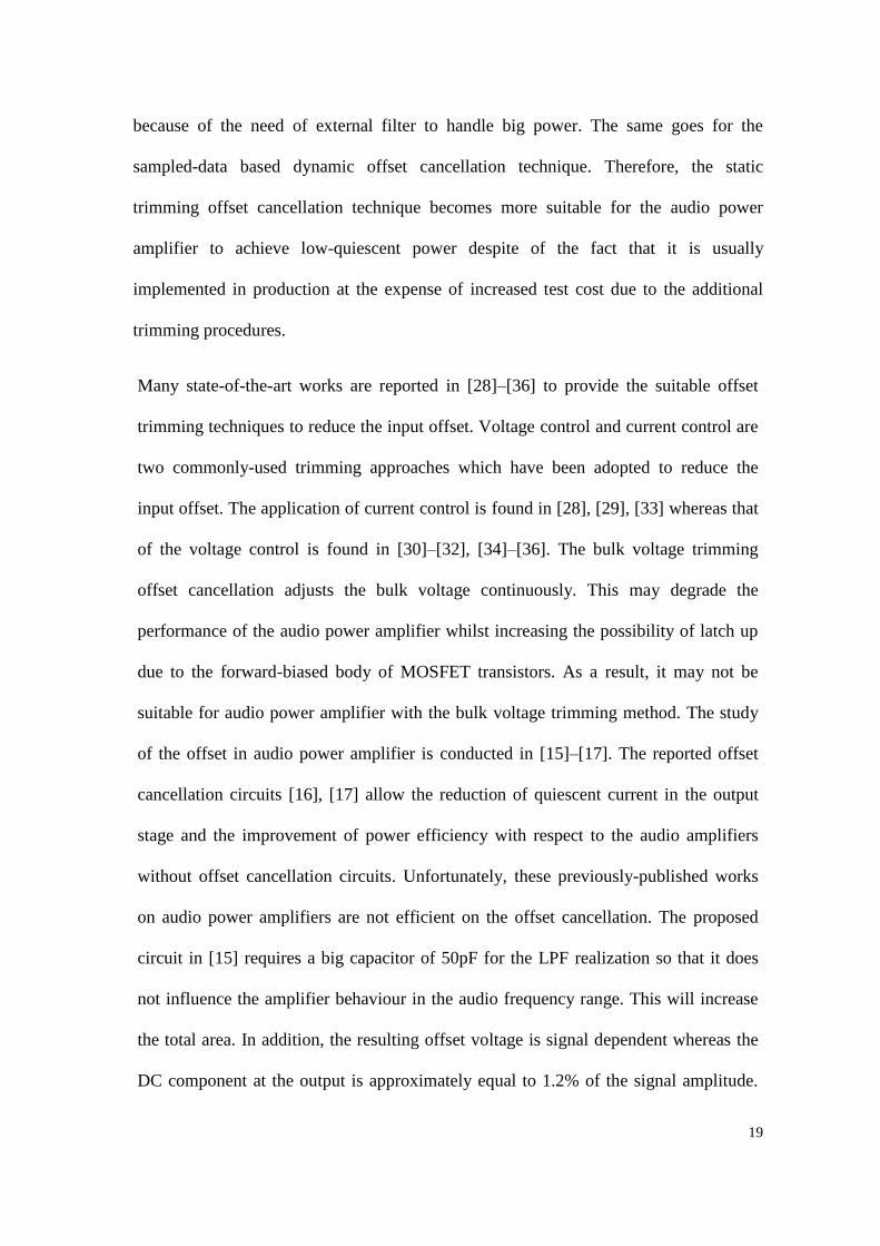
Many state-of-the-art works are reported in [28]–[36] to provide the suitable offset
trimming techniques to reduce the input offset. Voltage control and current control are
two commonly-used trimming approaches which have been adopted to reduce the
input offset. The application of current control is found in [28], [29], [33] whereas that
of the voltage control is found in [30]–[32], [34]–[36]. The bulk voltage trimming
offset cancellation adjusts the bulk voltage continuously. This may degrade the
performance of the audio power amplifier whilst increasing the possibility of latch up
due to the forward-biased body of MOSFET transistors. As a result, it may not be
suitable for audio power amplifier with the bulk voltage trimming method. The study
of the offset in audio power amplifier is conducted in [15]–[17]. The reported offset
cancellation circuits [16], [17] allow the reduction of quiescent current in the output
stage and the improvement of power efficiency with respect to the audio amplifiers
without offset cancellation circuits. Unfortunately, these previously-published works
on audio power amplifiers are not efficient on the offset cancellation. The proposed
circuit in [15] requires a big capacitor of 50pF for the LPF realization so that it does
not influence the amplifier behaviour in the audio frequency range. This will increase
the total area. In addition, the resulting offset voltage is signal dependent whereas the
DC component at the output is approximately equal to 1.2% of the signal amplitude.

20
The full analog approach [16] requires an external capacitor to realize the LPF.
Alternatively, a cross offset cancellation technique [17] can reduce the offset for class-
D amplifier but it is not suitable for class-AB application.
Control Signal
DAC
OPA
CO= 1 Yes
DOWN
No
UP
Up/Down
Counter
Cross Zero?
Comp
VOUT
Yes
Stop
Figure 2.7 Concept of offset calibration circuit proposed in [28].
For the headphone amplifier offset reduction, the automatic trimming offset
cancellation technique is more efficient than other mentioned techniques. Fig. 2.7
shows the exemplary signal flow of offset calibration circuit with current control.
However, the architecture has suffered from two disadvantages. The first one is that
the amplifier requires a ping-pong topology as shown in Fig. 2.8 to obtain the
continuous-time output signal. Unfortunately, it doubles the silicon area and power
consumption. The second one is that the ping-pong circuit architecture will contribute
additional switching noise which may not be desirable in high-performance audio
amplifier application. Due to this reason, there is a need to investigate an alternative
offset calibration scheme that overcomes the key disadvantages of the aforementioned
scheme.

21
OPA2
Control Signal 2 Control Signal 1
Vconf
Vin-
Vin+
Vout
Vot
P1
P1'
P1
P2
P2'
P2
P4
P4'
P4
P3
P3'
P3
P3
P3'
P3
P1
P1'
P1
OPA1
Figure 2.8 Topology of ping-pong operational amplifier proposed in [28].
2.3.1. Yu’s Circuit [28]
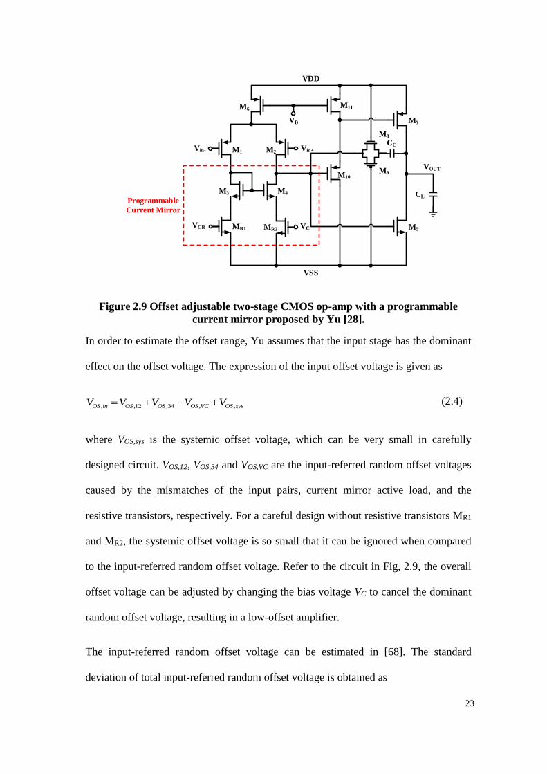
The main idea of Yu’s circuit is to digitally adjust the bias voltage of a programmable
current mirror, which serves as the active load of input pairs. Although the bias voltage
is changed to reduce the offset, it should be treated as current control like approach
[29], [33] since they all modify the offset by changing the biasing current of input
stage. The proposed amplifier by Yu is depicted in Fig. 2.9, in which the current mirror
is programmable and controllable by the output signal. The current mirror gain can be
digitally adjusted by changing the voltage of VCB and VC. This will adjust the input
offset consequently. The basic concept of the offset tuning architecture is illustrated in
Fig. 2.7. It consists of a comparator, an up-down-counter and a digital-to-analog
converter (DAC). Compared to other adjustable current mirror circuits, the digital

22
scheme can achieve relatively low offset and avoid charge injection problems. The
working principle of the calibration procedures are summarized as follows:
1) The output of the main amplifier is compared to a zero voltage when the two
terminals are connected to ground.
2) Then, the output of the comparator will be used to control the bias voltage VC
through an up-down-counter and a DAC to reduce the input offset of the main
amplifier.
3) Repeat procedure 1) and 2) until the output of the main amplifier crosses zero.
This algorithm is straight-forward and it can be applied in many offset cancellation
circuits. The resolution of the offset cancellation is limited by range of the bias voltage
VC and the comparator. In general, the resolution of the bias voltage is more important
than that of the comparator since the tuning block usually requires more power and
large area. The offset range of the main amplifier is determined firstly whilst the
cancellation should cover the whole offset range. Then the number of bits can be
determined to accomplish a specific resolution.
23
Vin+Vin-
VDD
VSS
M1 M2
M7
M5
VOUT
M6M11
M3 M4
MR1 MR2VCB VC
M10
M8
M9
CL
CC
VB
Programmable
Current Mirror
Figure 2.9 Offset adjustable two-stage CMOS op-amp with a programmable
current mirror proposed by Yu [28].
In order to estimate the offset range, Yu assumes that the input stage has the dominant
effect on the offset voltage. The expression of the input offset voltage is given as
, ,12 ,34 , ,OS in OS OS OS VC OS sysV V V V V (2.4)
where VOS,sys is the systemic offset voltage, which can be very small in carefully
designed circuit. VOS,12, VOS,34 and VOS,VC are the input-referred random offset voltages
caused by the mismatches of the input pairs, current mirror active load, and the
resistive transistors, respectively. For a careful design without resistive transistors MR1
and MR2, the systemic offset voltage is so small that it can be ignored when compared
to the input-referred random offset voltage. Refer to the circuit in Fig, 2.9, the overall
offset voltage can be adjusted by changing the bias voltage VC to cancel the dominant
random offset voltage, resulting in a low-offset amplifier.
The input-referred random offset voltage can be estimated in [68]. The standard
deviation of total input-referred random offset voltage is obtained as

24
gs1,2 T1,2 2 2
VOS L W2 2 2 2 2 2
1,2 3,4 VC 1,2 3,4 VC
2 2 2
VT1,2 VT3,4 VT,VC 1/2
2 2 2
gs,VC T,VCgs1,2 T1,2 gs3,4 T3,4
| V V | 1 1 1 1 1 1σ [σ σ
L L L W W W2
4σ 4σ σ]
(V V )V V V V
(2.5)
where Vgs1,2, VT1,2, L1,2 and W1,2 are the gate-source voltage, the threshold voltage, the
channel length and the width of transistors M1 and M2, respectively. Based on the
transistors size and [68], the input-referred random offset voltage can be estimated
with value of σVOS = 12.2mV. 3σVOS almost can cover 99.7% of the offset and it is
selected as the compensation range of offset cancellation.
Meanwhile, the range of the bias voltage can be determined by simulation, which is
accomplished by a resistor ladder based digital-to-analog converter. In order to achieve
full duty cycle, a ping-pong structure is applied in Yu’s circuit. It is made up of two
identically op-amps shown in Fig. 2.9. When one op-amp works in the normal
amplifying mode, the other one will operate in the offset cancellation mode. By
changing the operating mode of the two op-amps, a low-offset amplifier can be
obtained with the ping-pong topology.

25
2.4. Review of Frequency Compensation Techniques
An effective frequency compensation scheme plays one of the key roles in low-
quiescent headphone amplifier design. The frequency compensation of a headphone
amplifier has displayed some differences with that of a capacitive load driven
operational amplifier (op-amp). It is mainly because that the DC gain of last stage of
headphone amplifier is usually smaller than or close to unity in the presence of very
small resistive load. Besides, the output pole frequency contributed by the effective
load is usually located at high frequency which is above the audio band. As such, it can
be ignored in the frequency compensation analysis. Nevertheless, the frequency
compensation techniques used for capacitive load driven op-amp can also be extended
or used in headphone amplifier. For better low-quiescent performance, the frequency
compensation needs to be addressed.
-gm1 -gm3+gm2
Cm1
Cm2
Cp1ro1 ro2 Cp2 RL CL
Vin Vout
Figure 2.10 Topology of three-stage NMC amplifier [37].
The nested Miller compensation (NMC) amplifier [37], [50] is the foundation circuit
which serves as the benchmark for other multistage amplifiers. The small-signal
analysis of headphone amplifier is similar to that of the capacitive driven op-amp
except that the third-stage gain of headphone amplifier tends to be small due to very

26
low resistive load. The following assumptions are made when analysing the small-
signal behaviour of NMC headphone amplifier:
1) The first two stages have gain much higher than one (gmiroi »1) whereas the gain of
output stage is lower than one (gm3*RL «1).
2) The loading capacitance CL is much larger than all of the other capacitances (CL »
Cpi, Cmi), including the compensation capacitors and the lumped capacitances. The
lumped parasitic capacitance of the first stage is much smaller than the
compensation capacitance (Cm1 » Cp1).
3) The interstage capacitances can be ignored.
The output resistances, equivalent transconductance and lumped parasitic capacitances
of each gain stage are denoted by roi, gmi and Cpi, respectively. Cm1 and Cm2 are the
Miller capacitors. RL is the resistive load. The transfer function of NMC amplifier is
obtained as
22 1 2
3 2 3
23 2 2 2 2
3 2 3 2 3
1
(1 )(1 )
m m m
m m mdc
L m m m m L m
dB m m m m
C C Cs s
g g gA s A
g g C g C C Css s
p g g g g
(2.6)
1 2 3 1 2dc m m m o o LA g g g r r R (2.7)
3
1 2 3 1 2
1dB
m m m o o L
pC g g r r R
(2.8)
It shows that the headphone amplifier frequency response has the same dominant pole
expression as that of the capacitive driven op-amp. The expressions of the first zero
and non-dominant pole are obtained as follows:
27
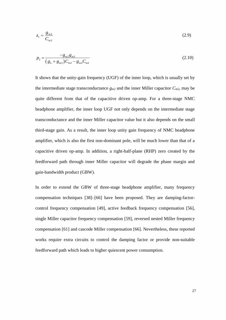
31
2
m
m
gz
C (2.9)
2 3
2
3 2 2 2
m m
L m m m m
g gp
g g C g C
(2.10)
It shows that the unity-gain frequency (UGF) of the inner loop, which is usually set by
the intermediate stage transconductance gm2 and the inner Miller capacitor Cm2, may be
quite different from that of the capacitive driven op-amp. For a three-stage NMC
headphone amplifier, the inner loop UGF not only depends on the intermediate stage
transconductance and the inner Miller capacitor value but it also depends on the small
third-stage gain. As a result, the inner loop unity gain frequency of NMC headphone
amplifier, which is also the first non-dominant pole, will be much lower than that of a
capacitive driven op-amp. In addition, a right-half-plane (RHP) zero created by the
feedforward path through inner Miller capacitor will degrade the phase margin and
gain-bandwidth product (GBW).
In order to extend the GBW of three-stage headphone amplifier, many frequency
compensation techniques [38]–[66] have been proposed. They are damping-factor-
control frequency compensation [49], active feedback frequency compensation [56],
single Miller capacitor frequency compensation [59], reversed nested Miller frequency
compensation [61] and cascode Miller compensation [66]. Nevertheless, these reported
works require extra circuits to control the damping factor or provide non-suitable
feedforward path which leads to higher quiescent power consumption.
28
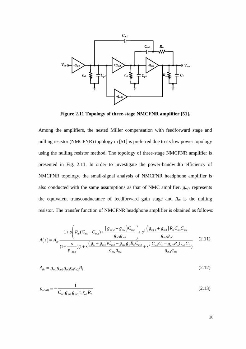
-gm1 -gm3+gm2
Cm1
Cm2 Rm
Cp1ro1 ro2 Cp2RL CL
Vin Vout
-gmf2
Figure 2.11 Topology of three-stage NMCFNR amplifier [51].
Among the amplifiers, the nested Miller compensation with feedforward stage and
nulling resistor (NMCFNR) topology in [51] is preferred due to its low power topology
using the nulling resistor method. The topology of three-stage NMCFNR amplifier is
presented in Fig. 2.11. In order to investigate the power-bandwidth efficiency of
NMCFNR topology, the small-signal analysis of NMCFNR headphone amplifier is
also conducted with the same assumptions as that of NMC amplifier. gmf2 represents
the equivalent transconductance of feedforward gain stage and Rm is the nulling
resistor. The transfer function of NMCFNR headphone amplifier is obtained as follows:
2 2 2 2 3 1 22
1 2
3 2 2 3
23 2 2 2 2 2 2
3 2 3 2 3
1 ( )
(1 )(1 )
mf m m mf m m m m
m m m
m m m m
dc
L m m m L m m m L m m m L
dB m m m m
g g C g g R C Cs R C C s
g g g gA s A
g g C g g R C C C g R C Css s
p g g g g
(2.11)
1 2 3 1 2dc m m m o o LA g g g r r R (2.12)
3
1 2 3 1 2
1dB
m m m o o L
pC g g r r R
(2.13)

29
where Adc and p-3dB have the same expressions as that of the NMC amplifier. Since the
non-dominant high frequency zeros and poles are far away from the UGF, one can
obtain the first zero and second pole as follows:
2 3
1
2 3 1 2 2 2 2
m m
m m m m m mf m m
g gz
g g R C C g g C
(2.14)
2 3
2
3 2 2 2
m m
L m m m L m m
g gp
g g C g g R C
(2.15)
For the feedforward transconductance gmf2 > gm2 in (2.14), the left-half-plane (LHP)
zero is created. The price paid for the large gmf2 is that it will increase the power
consumption. If gmf2 < gm2 is made for low-power criteria, the control of LHP zero will
rely on the increased value of nulling resistor Rm [51]. However, the disadvantage of
NMCFNR topology is that the LHP pole in (2.14) has the possibility to become a RHP
pole when there is a substantial increase of the product gLRm. To avoid the formation of
RHP pole and permit the better placement of the second pole close to the first zero, a
three-stage NMCFNR headphone amplifier will be resorted to the tradeoff design
among the extra power needed for gmf2 and the allowable resistance range of Rm. As a
result, the constraint value for Rm will result in the decrease of the GBW. The outcome
is the increase of Miller compensation capacitors, Cm1 and Cm2, to guarantee the
stability if low-power design is of concern.

30
Chapter 3 Architecture and Circuit Design
3.1. Proposed Digitally-Assisted Offset Calibration Circuit
3.1.1. Architecture of Proposed Digitally-Assisted Low-offset
Headphone Amplifier
Of particular design criteria, it is important that the performance parameters, such as
THD+N, SNR, PSRR and so forth remain unchanged when the offset calibration
techniques are applied. The widely used dynamic offset techniques may not be
appropriate for implementation because the smoothing filter needs to handle high
power in the APA. For this reason, the automatic control that deals with active load
trimming [28] or current injection [29] with ping-pong topology will be suitable to
reduce the input-referred offset of headphone amplifier. However, the single-ended
high-impedance node current injection circuit [29] degrades the PSRR due to the
unbalanced supply noise path and reduces the effective DC gain of first gain stage.
Although the active load trimming with ping-pong topology provides another means to
counteract the offset problem, it is at the expense of doubling the silicon area and
power consumption. In addition, the ping-pong topology may introduce additional
switching noise in the continuous-time process of swap action on the two amplifiers.
This is considered undesirable effect in headphone amplifier design. In order to tackle
these problems, Fig. 3.1 depicts a digitally-assisted low-offset headphone amplifier
incorporating the proposed offset calibration circuit.

31
R2=R3=R4=10kΩ R1'=9.8kΩ R1"=200Ω
VOUT
VIN-
R2R1"R1'
Y
X
R3
R4
VOFF
S1
S2
Digitally-assisted
Offset Calibration
Circuit
Balanced Offset Compensation Current (IB4 - IB2)
Dummy Current (IB3 - IB1)
Done
`
VOUT Offset Compensation
Current DAC
Power-On
Reset CircuitEnable
<7:0>
Up/Down
PoR
VCOMP
Done
Balanced Offset
Compensation
Current
Dummy
CurrentComparator
RL CL
VIN+
CAL_CLK
Up/Down
Counter
Preset
CLK
Zero-Crossing
Detection Logic
CAL_En
Input
Comparator
Spike Removal
Circuit
VCOMP'
Cal_on_Req
Figure 3.1 The headphone amplifier with the proposed digitally-assisted offset
calibration circuit.
Refer to the offset calibration circuit in Fig. 3.1, it consists of a comparator, a
comparator spike removal circuit, a zero-crossing detection logic, a power-on reset
circuit, an up-down-counter, a balanced offset compensation current injection circuit
and some control logic gates. The offset voltage is calibrated through digitally
adjusting the current injected into a pair of low impedance nodes in the differential
input stage on the basis of balance design approach.
As shown in Fig. 3.1, Cal_on_Req (Calibration on Request) is a user-demand or
system control signal. Since the proposed offset calibration circuit cannot eliminate the
effect of the temperature on the offset voltage, the Cal_on_Req signal may be used by
system to activate the offset calibration when there is a need to reduce the increase of

32
offset under the temperature variation. It is applied in a form of signal pulse format.
When the pulse's logic is at high value, it enables the zero-crossing detection logic by
setting the logic high output. When the pulse’s logic is at low value, it enables the up-
down-counter of the system. Normally, this input control signal remains at logic zero.
The offset calibration system is automatically started in the beginning of power-up
action. During the start-up transition of the amplifier, the power-on reset circuit goes
logic high. Since the Cal_on_Req remains at logic low, the output of zero-crossing
detection logic is set to logic high through the internal edge-triggered flip flop as the
memory. Meanwhile, the digital outputs of the up-down-counter are in preset state
having the middle logic value of 1000,0000. When the startup has completed in a short
duration, the power-on reset circuit gives logic low output. Then, the up-down-counter
carries out the offset calibration task, dependent upon the up/down‾‾‾‾ control signal
whilst the Cal_on_Req remains low. In the offset calibration mode, the two switches,
S1 and S2, are closed while the amplifier is set to have the default DC gain of about 51
with respect to the unknown amplifier’s input offset voltage to be calibrated. This DC
gain is chosen so that the input offset can be amplified so that the resolution of the
offset calibration is not significantly degraded by the comparator’s offset. In the
process of offset calibration, the up-down-counter controls the digitally injecting
current into the differential stage. As a result, the input-referred offset and the
headphone amplifier output are digitally reduced to the resolution of design. The
comparator spike removal circuit is responsible to remove the false analog signal
caused by the spike appeared at the analog output of headphone amplifier during the
switching action of offset current injection circuit. During calibration, there is no
polarity change at the output of comparator. When the zero-crossing detection logic

33
detects the transition change, either from logic high to low or from logic low to high at
the output of comparator, its output goes low to terminate the offset calibration process.
Finally, in the normal operation mode, the two switches, S1 and S2 open and the up-
down-counter is disabled. At this juncture, the headphone amplifier will serve as a
driver.
0.0 1.0m 2.0m 3.0m 4.0m
-1.2
-0.6
0.0
0.6
1.2
-1.0-0.50.00.51.0
-0.4-0.20.00.20.4
Don
e (V
)
Time (s)
Power-on Reset Period
VC
OM
P (
V)
t = 2.96ms
NormalOperation
OffsetCalibration
VO
UT (
V)
t = 20s t = 2mst = 2.96ms
t = 2.96ms
Figure 3.2 Simulated transient response of the important signals in the offset
calibration system.
Fig. 3.2 shows the simulated transient response of the key signals in the offset
calibration system. After the power-on reset period from 20µs-2ms, the output-referred
offset of the amplifier is automatically trimmed from about 2ms to 2.96ms. The zoom-
in view of the output signal shows that VOUT settles to the value of −4.1mV under
which the offset calibration stops. This is translated to the input offset voltage of
−80.4µV based on the closed-loop gain of 51 in offset calibration mode. For the VCOMP,
there exists several transition waveforms in the form of either short pulse or periodic

34
transient output response. They come from (i) the system start-up with the short
duration pulse at time 20µs, (ii) the completion of the first offset calibration with the
short duration pulse at about 2.96ms and (iii) the output response of comparison based
on the periodical input signal after 2.96ms. In this design, when the zero-crossing
detection logic detects the transition change of signal VCOMP at about 2.96ms which is
the end time of offset calibration, the Done‾‾‾‾ signal becomes asserted low. Other
subsequent change of transitions from VCOMP will not influence the status of Done‾‾‾‾
signal.
3.1.2. Transistor Level of Digitally-Assisted Offset Calibration Circuit
3.1.2.1. Balanced Offset Compensation Current Injection Circuit
VDD
Vin+Vin-
VSS
M1
M3 M4
M6 M7
M5
VBP2
VBN2
VBN1
VBP1
Differential Input Stage
M2
M10 M11
M9M8
IB2
IB4
IB1
IB3
YX
IX IY
Digitally Programmable
Current Source
Figure 3.3 Concept of balanced offset compensation current injected into
differential input stage.
The key idea for obtaining low offset circuit is to inject balanced offset compensation
current into the differential stage of the amplifier in order to digitally adjust the input-

35
referred offset voltage of the amplifier system. Refer to Fig. 3.3, IB1 ~ IB3 represent
three constant current sources, which have the same value. IB4 is a digitally
programmable current source that can be digitally adjusted by the outputs of the up-
down-counter. IX and IY represent the current injected into the node X and Y,
respectively. Since IB1 and IB3 have the same value, the current injected into node Y
will be almost zero. The main function of this dummy signal path is used to cancel the
supply noise from node X, which will be further explained in the following part.
B0 B2 B4 B6B1 B3 B5 B7
I0 2 I0 8 I0 32 I04 I0 16 I0 64 I0 128 I0 IB3=128 I0
I0
IB1=128 I0IB2=128 I0
VDD
VSS
YX
VBN5 VBN6
Current Source Array for LSB Current Source Array for MSB
LSB MSB
×1 ×2 ×4 ×8×1 ×1 ×2 ×4 ×8 ×8
Figure 3.4 Transistor level of four current sources for balanced current injection.
Fig. 3.4 shows the transistor level of the balanced offset compensation current
injection circuit. The value of three constant current sources IB1 ~ IB3 are equal to
128I0. The digitally programmable current source, IB4, consists of two current source
arrays, which are controlled by a total of eight switches. The eight-bit current control is
chosen such that it can cover a wide range of the input-referred offset value. IB4 can
vary from 0 to 255I0. At this juncture, it is set to be 128I0 as a default value from the
outputs of up-down-counter before the start of offset calibration process. VBN5 and
VBN6 are the bias voltages for the LSB current source array and MSB current source
array, respectively. In each array, the transistor current sources are binary weighted in
36
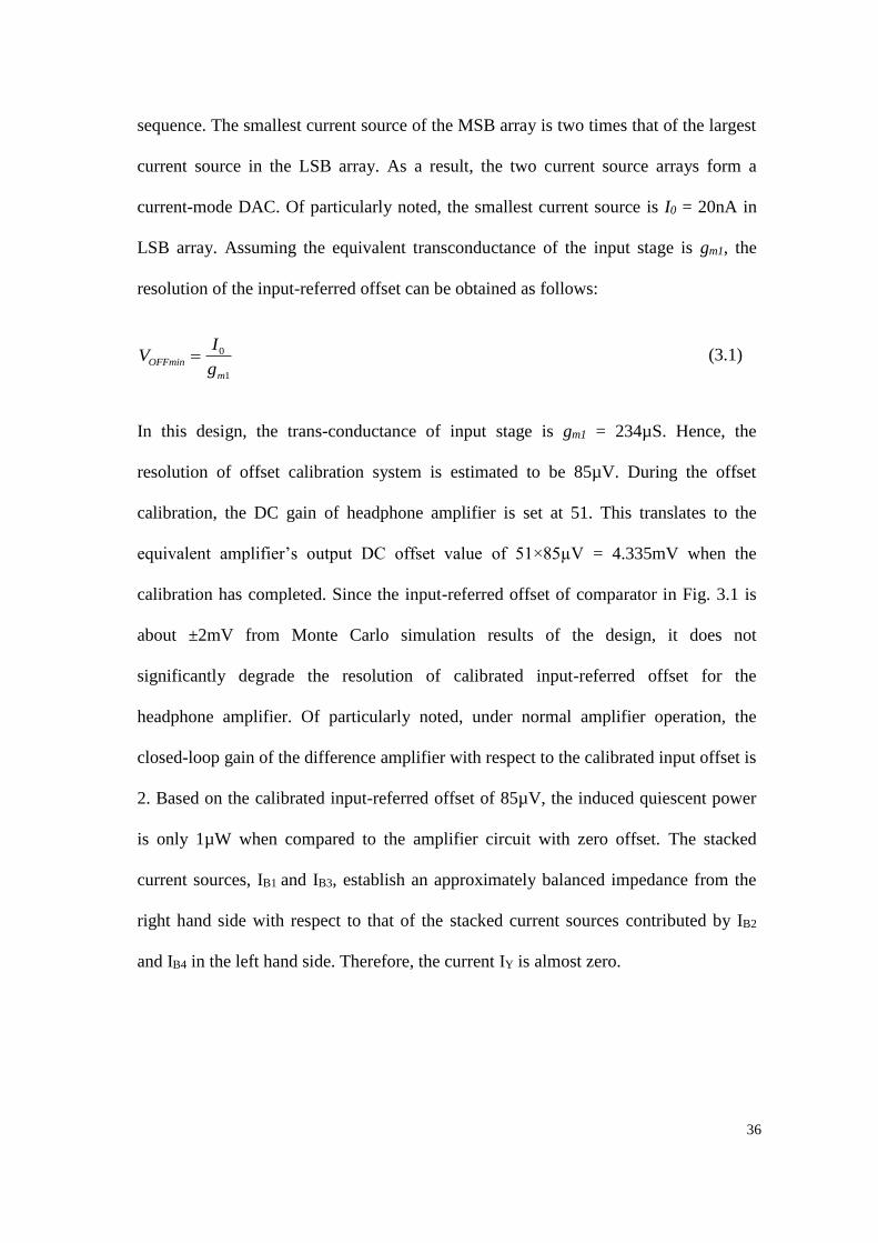
sequence. The smallest current source of the MSB array is two times that of the largest
current source in the LSB array. As a result, the two current source arrays form a
current-mode DAC. Of particularly noted, the smallest current source is I0 = 20nA in
LSB array. Assuming the equivalent transconductance of the input stage is gm1, the
resolution of the input-referred offset can be obtained as follows:
0
1
OFFmin
m
IV
g (3.1)
In this design, the trans-conductance of input stage is gm1 = 234µS. Hence, the
resolution of offset calibration system is estimated to be 85µV. During the offset
calibration, the DC gain of headphone amplifier is set at 51. This translates to the
equivalent amplifier’s output DC offset value of 51×85µV = 4.335mV when the
calibration has completed. Since the input-referred offset of comparator in Fig. 3.1 is
about ±2mV from Monte Carlo simulation results of the design, it does not
significantly degrade the resolution of calibrated input-referred offset for the
headphone amplifier. Of particularly noted, under normal amplifier operation, the
closed-loop gain of the difference amplifier with respect to the calibrated input offset is
2. Based on the calibrated input-referred offset of 85µV, the induced quiescent power
is only 1µW when compared to the amplifier circuit with zero offset. The stacked
current sources, IB1 and IB3, establish an approximately balanced impedance from the
right hand side with respect to that of the stacked current sources contributed by IB2
and IB4 in the left hand side. Therefore, the current IY is almost zero.
37
3.1.2.2. Other Circuit Blocks of the Offset Calibration Circuit
Except for the balanced offset compensation current injection circuit, the offset
calibration circuit also consists of five major circuit blocks. They are comparator,
comparator spike removal circuit, zero-crossing detection logic, power-on reset and
up-down-counter. The comparator is realized by a simple operational transconductance
amplifier (OTA), which supports rail-to-rail output. The positive and negative
terminals of the OTA are connected to the output of headphone amplifier and the
ground at 0V, respectively. The comparator is designed to ensure that the resolution of
offset calibration circuit is not greatly degraded. The function of comparator spike
removal circuit aims to remove the spikes produced from the headphone amplifier
output signal that will falsely trigger the zero-crossing detection logic to produce the
false digital output in a form of short duration transition pulse. The comparator spike
removal detector circuit is realized by an edge-triggered D-type flip-flop. This is used
to synchronize with the long duration calibration clock so as to discriminate against the
false digital signal in a form of short transition pulses which are caused by the analog
spikes at the input of the comparator. The up-down-counter is a conventional
bidirectional counter which comprises eight JK flip-flops and other necessary logic
gates. When the amplifier works in the offset calibration mode, the up-down-counter
and the amplifier generates an eight-bit digital signal to adjust the weighted current
injected into the differential stage. Shown in Fig. 3.5, the power-on reset is made up of
a voltage divider, an RC circuit, a comparator and a digital buffer. In order to realize a
large time constant and save the silicon area, a pseudo resistor is employed to achieve
a high resistance value.

38
VDD
R1
R2
VSS
RM1
C
ComparatorBuffer
PoR
V1VR
Figure 3.5 Power-on reset circuit.
0.0 1.0m 2.0m 3.0m 4.0m
-1.0
-0.5
0.0
0.5
1.0
-0.9
-0.6
-0.3
0.0
PoR
(V)
Time(s)
V1(V
)
Figure 3.6 Transient response of the power-on reset circuit when the amplifier
starts up.
The transient response of the power-on reset circuit is illustrated in Fig. 3.6. At the
beginning of the startup, the momentary negative pulse generated from VSS couples to
the negative input V1 of comparator, it forces the reset circuit output PoR to go high.
V1 gradually settles to a constant voltage VR of 200mV defined by the voltage divider.
When V1 is smaller than 0V, the comparator output, VOUT, gives logic “0”, which is
−1V. When V1 reaches above 0V, the VOUT turns to logic “1” which is 1V. It is noted

39
that the choice of 200mV is to allow a suitable pulse width of about 2ms to be
generated from the power-on reset circuit output. During this startup period, the zero-
crossing detection logic is enabled whereas the up-down-counter is in preset state.
Immediately after the period, the offset calibration process will be started in the APA.
Fig. 3.7 shows the circuit of zero-crossing detection logic, which is realized using a
complementary delay generation circuit, an XNOR gate, a D-type flip-flop and an
inverting output buffer. Whenever any logic transition appears at the output of
comparator, it is sensed by the single input of zero-crossing detection logic. On the
other hand, the output “Done‾‾‾‾ ” of zero-detector, which comes from the cascade of
inverting buffer and D-type flip flop, is set to logic high by the Cal_Enable signal prior
to start the offset calibration.
VCOMP
VDDDone
VDD
VSS
VIN INV Buf
CAL_Enable
VXNOR
D Q
Clk
QCLR
MZ,1 MZ,3 MZ,5
MZ,2 MZ,4 MZ,6 MZ,8
MZ,9MZ,7
MZ,10
MZ,11
MZ,13 MZ,14 MZ,19
MZ,18
MZ,20
MZ,17
MZ,15MZ,16
MZ,12
MZ,21
MZ,22
VCOMP
Figure 3.7 Zero-crossing detection logic.

40
0.0 1.0m 2.0m 3.0m 4.0m
-1.0-0.50.00.51.0
-1.0-0.50.00.51.0
-1.0-0.50.00.51.0
Do
ne
(V)
Time (s)
VX
NO
R (
V)
CalibrationOffset
Power-on Reset Period
VC
OM
P'
(V)
t = 20s t = 2ms t = 2.96ms
t = 2.96ms
t = 2.96ms
OperationNormal
Figure 3.8 Transient responses of the signals in zero-crossing detection logic.
Fig. 3.8 shows the transient responses of some signals in zero-crossing detection logic.
The complementary delay generation circuit within the detector produces the dual
logic signals which have the complementary and delay characteristics. The signals
VCOMP is the output of the comparator spike removal circuit shown in Fig. 3.1 and
VCOMP‾‾‾‾‾ is the delayed inverting value of VCOMP. The VCOMP and VCOMP‾‾‾‾‾ are tied to the
inputs of XNOR gate. The XNOR gate generates a short pulse signal if the comparator
spike removal circuit outputs the real detected transition. When the positive transition
of the short pulse appears at the clock input of D flip flop, the output signal Done‾‾‾‾ of
the zero-crossing detection logic changes from logic high to logic low, indicating that
the calibration has completed. At this juncture, the Done‾‾‾‾ signal opens the amplifier
switches as depicted in Fig. 3.1 and stops the up-down-counter. The amplifier goes
into normal operation mode. Fig. 3.8 shows the comparator spike removal circuit
output, VCOMP, in response to the application of a 1kHz sinusoidal input signal to the
41
APA with 2mV input offset, starting from the system power up at time 20µs to the
power-on reset period 20µs-2ms. Then, this is followed by the offset calibration period
between 2ms-2.96ms and the normal operation mode after 2.96ms. It is important to
note that the calibration period depends on the input offset of APA. When the zero-
crossing detection logic in Fig. 3.7 detects the transition change of signal VCOMP, it
generates a pulse signal VXNOR. The Done‾‾‾‾ signal, which is obtained from the inverting
buffer output of the D-type flip-flop, is only asserted one time when the offset
calibration has completed. It remains active low until the Cal_on_Req signal has been
triggered to initiate another offset calibration by system or user demand. Other
transition changes do not influence the status of Done‾‾‾‾ signal.

42
3.1.3. Influence of Input-offset, Temperature and Power Transistors
Leakage Current on Quiescent Power Consumption of Headphone
Amplifier
The quiescent power consumption of a power amplifier is mainly influenced by the
input- referred offset, temperature and power transistors leakage current. In order to
study the influence of input-referred offset voltage and temperature on the quiescent
power consumption without offset calibration, the quiescent power of this amplifier
under different temperatures and VOFFSET values is used as example to illustrate the
effects. The simulation results are obtained and summarized in Table 3.1 and Fig. 3.9.
Table 3.1 The Offset-induced Quiescent Power Consumption Study of Headphone
Amplifier
VOFFSET
Offset-
Induced
Current
(mA)
Total
Quiescent
Power (mW)
Quiescent Power Increase
with respect to APA with
0mV Offset
0mV 0 0.4295 0%
1mV 0.125 0.4811 12.01%
2mV 0.25 0.5798 34.99%
3mV 0.375 0.6931 61.37%
4mV 0.5 0.8119 89.03%
5mV 0.625 0.9330 117.2%
It can be observed that the total quiescent power consumption increases with the input-
referred offset voltage. The simulation results have revealed that the quiescent power
consumption will increase by 117.2% for a 5mV input-referred offset. This suggests
that the offset-related quiescent power becomes a significant part in the total power
consumption. The offset-induced quiescent power study has confirmed the fact that the
low-offset metric is necessary for a low-quiescent power amplifier design.

43
-5.00m -2.50m 0.00 2.50m 5.00m
400.0μ
600.0μ
800.0μ
1.0m
Tota
l Q
uie
scen
t P
ow
er (
W)
Input Offset (V)
T = 85 oC
T = 27 oC
T = -40 oC
Figure 3.9 The quiescent power consumption of proposed power amplifier under
different temperature and input-referred offset voltage.
The dependence of total quiescent power consumption of the headphone amplifier on
temperature is mainly determined by the biasing circuit. A constant-gm bias generation
circuit is used in the amplifier. According to the working principle of constant-gm
circuit, the dependence of current on temperature is determined by carrier mobility,
threshold voltage and resistor value. Fig. 3.9 shows that the quiescent power
consumption will increase with temperature. It is mainly because the threshold voltage
is the dominant factor which decreases with temperature, causing the increase of gate-
source difference voltage bias on the resistor.
The leakage current may be another factor that may affect the total quiescent power
consumption of headphone amplifier in nano-scaled technology. Power transistors with
large aspect ratio will become the dominant sources for the leakage current. In the
quiescent condition of headphone amplifier, the drain voltage of the power transistors
are 0V. In order to identify the value of leakage current and understand its variation

44
with temperature, the gates of the power transistors are connected to the positive
supply and negative supply, respectively.
-40 -20 0 20 40 60 80 100
0
100n
200n
300n
400n
Lea
ka
ge
Cu
rren
t (A
)
Temperature (oC)
Power Transistors in FF Corners
Power Transistors in TT Corners
Power Transistors in SS Corners
Figure 3.10 Temperature variation of power transistors leakage current with in
different corners.
Fig. 3.10 shows the temperature variation of power transistors leakage current in
different corners. It shows that the leakage current of power transistors in fast-fast (FF)
corner is much higher than that of other corners. It is because the threshold voltage of
transistors in FF corners is smaller. The leakage current increases rapidly with
temperature and it is much smaller than the quiescent power consumption of headphone
amplifier. Therefore, we can conclude that the leakage current will not degrade the
quiescent power consumption of power amplifier despite leakage current is often as one
of the main issues in VLSI system.

45
3.1.4. Advantages of Balanced Low-impedance Node Current
Injection Circuit
Compared to the conventional single-ended high impedance node current injection, the
proposed balanced topology in this work has offered two key advantages.
Firstly, since the high-impedance offset compensation current sources are injected into
two low-impedance nodes of folded-cascode input stage, it will not significantly
degrade the gain of first stage. Secondly, when the current injection circuit is coupled
to the output of first stage, it may jeopardize the PSRR significantly due to the
unbalanced topology. Fig. 3.11 shows the PSRR simulation results for the amplifiers
designed with two different current injection circuits. The amplifier design without any
current injection circuit serves as the benchmark. Fig. 3.11 (a) compares the PSRR
plots for the amplifier with/without balanced offset current injection compensation. It
shows that the PSRR obtained from the proposed balanced offset compensated
amplifier approximately maintains similar low-frequency PSRR characteristic with
reference to that of the benchmark. By comparison, the low frequency PSRR of
conventional offset current injection compensation is much lower than that of the
benchmark shown in Fig. 3.11 (b). For the critical frequency of 217Hz in mobile
applications, the current injection network causes the drop of 13dB in PSRR. It is
mainly because the conventional current injection circuit yields an additional supply
noise path from the supply to the critical node X in the input differential stage. The
implementation of balanced circuit topology introduces a dummy current branch,
which not only provides a symmetrical signal path for cancelling the supply noise but
it also balances the impedances associated with the critical nodes X and Y.
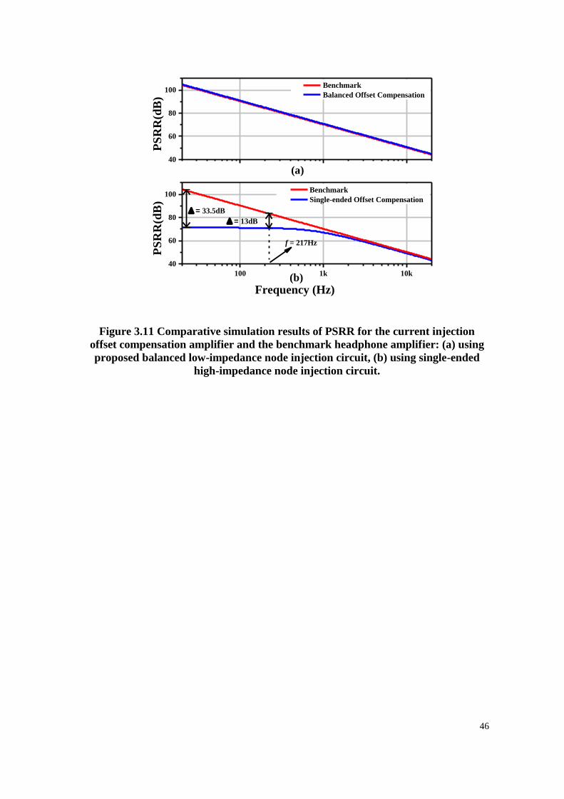
46
100 1k 10k
40
60
80
100
40
60
80
100
(b)
PS
RR
(dB
)
Frequency (Hz)
(a)
= 33.5dB
f = 217Hz
= 13dB
Benchmark
Single-ended Offset Compensation
Benchmark
Balanced Offset Compensation
PS
RR
(dB
)
Figure 3.11 Comparative simulation results of PSRR for the current injection
offset compensation amplifier and the benchmark headphone amplifier: (a) using
proposed balanced low-impedance node injection circuit, (b) using single-ended
high-impedance node injection circuit.
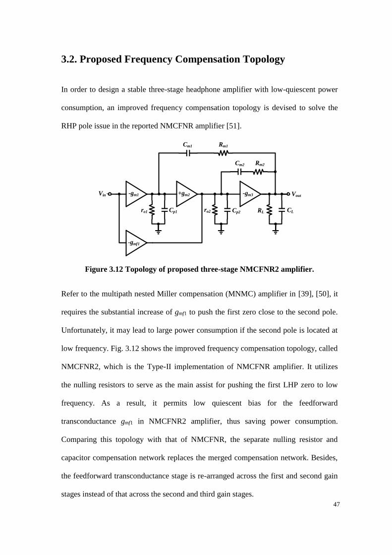
47
3.2. Proposed Frequency Compensation Topology
In order to design a stable three-stage headphone amplifier with low-quiescent power
consumption, an improved frequency compensation topology is devised to solve the
RHP pole issue in the reported NMCFNR amplifier [51].
-gm1 -gm3+gm2
-gmf1
Cm1
Cm2
Rm1
Rm2
Cp1ro1 ro2 Cp2 RL CL
Vin Vout
Figure 3.12 Topology of proposed three-stage NMCFNR2 amplifier.
Refer to the multipath nested Miller compensation (MNMC) amplifier in [39], [50], it
requires the substantial increase of gmf1 to push the first zero close to the second pole.
Unfortunately, it may lead to large power consumption if the second pole is located at
low frequency. Fig. 3.12 shows the improved frequency compensation topology, called
NMCFNR2, which is the Type-II implementation of NMCFNR amplifier. It utilizes
the nulling resistors to serve as the main assist for pushing the first LHP zero to low
frequency. As a result, it permits low quiescent bias for the feedforward
transconductance gmf1 in NMCFNR2 amplifier, thus saving power consumption.
Comparing this topology with that of NMCFNR, the separate nulling resistor and
capacitor compensation network replaces the merged compensation network. Besides,
the feedforward transconductance stage is re-arranged across the first and second gain
stages instead of that across the second and third gain stages.
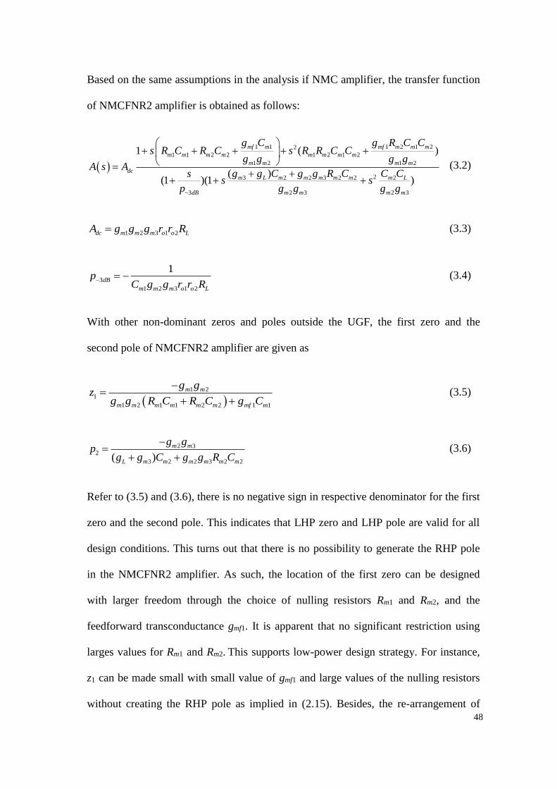
48
Based on the same assumptions in the analysis if NMC amplifier, the transfer function
of NMCFNR2 amplifier is obtained as follows:
1 1 1 2 1 22
1 1 2 2 1 2 1 2
1 2 1 2
23 2 2 3 2 2 2
3 2 3 2 3
1 ( )
( )(1 )(1 )
mf m mf m m m
m m m m m m m m
m m m m
dcm L m m m m m m L
dB m m m m
g C g R C Cs R C R C s R R C C
g g g gA s A
g g C g g R C C Css s
p g g g g
(3.2)
1 2 3 1 2dc m m m o o LA g g g r r R (3.3)
3
1 2 3 1 2
1dB
m m m o o L
pC g g r r R
(3.4)
With other non-dominant zeros and poles outside the UGF, the first zero and the
second pole of NMCFNR2 amplifier are given as
1 2
1
1 2 1 1 2 2 1 1
m m
m m m m m m mf m
g gz
g g R C R C g C
(3.5)
2 32
3 2 2 3 2 2( )
m m
L m m m m m m
g gp
g g C g g R C
(3.6)
Refer to (3.5) and (3.6), there is no negative sign in respective denominator for the first
zero and the second pole. This indicates that LHP zero and LHP pole are valid for all
design conditions. This turns out that there is no possibility to generate the RHP pole
in the NMCFNR2 amplifier. As such, the location of the first zero can be designed
with larger freedom through the choice of nulling resistors Rm1 and Rm2, and the
feedforward transconductance gmf1. It is apparent that no significant restriction using
larges values for Rm1 and Rm2. This supports low-power design strategy. For instance,
z1 can be made small with small value of gmf1 and large values of the nulling resistors
without creating the RHP pole as implied in (2.15). Besides, the re-arrangement of

49
feedforward topology in APA design causes gmf1Cm1/gm1gm2 in (3.5) > (gmf2-
gm2)Cm2/gm2gm3 in (2.14). Therefore, smaller Miller capacitor Cm1 can be employed for
defining the first LHP zero location according to (3.5). This gives the advantages of
small compensation capacitance as well as improved GBW.
100m 1 10 100 1k 10k 100k 1M 10M 100M
0
90
180
270
360
-80
-40
0
40
80
120
15k
5k
10k
0
20k
Ph
ase
(D
eg)
Frequency (Hz)
20k
0
5k
15k
Ga
in (
dB
)
10k
100m 1 10 100 1k 10k 100k 1M 10M 100M
-45
0
45
90
135
180
-80
-40
0
40
80
120
0
20k15k
10k
5k
Ph
ase
(D
eg)
Frequency (Hz)
5k
15k
10k
20k
Gain
(d
B)
0
(a)
(b)
Figure 3.13 Simulated open-loop gain and phase with different nulling resistors for
(a) NMCFNR2 amplifier and (b) NMCFNR amplifier.
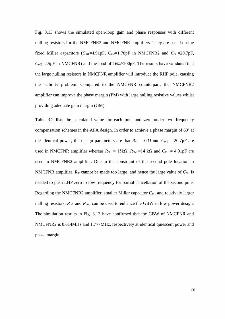
50
Fig. 3.13 shows the simulated open-loop gain and phase responses with different
nulling resistors for the NMCFNR2 and NMCFNR amplifiers. They are based on the
fixed Miller capacitors (Cm1=4.91pF, Cm2=1.78pF in NMCFNR2 and Cm1=20.7pF,
Cm2=2.5pF in NMCFNR) and the load of 16Ώ//200pF. The results have validated that
the large nulling resistors in NMCFNR amplifier will introduce the RHP pole, causing
the stability problem. Compared to the NMCFNR counterpart, the NMCFNR2
amplifier can improve the phase margin (PM) with large nulling resistive values whilst
providing adequate gain margin (GM).
Table 3.2 lists the calculated value for each pole and zero under two frequency
compensation schemes in the APA design. In order to achieve a phase margin of 60º at
the identical power, the design parameters are that Rm = 5kΩ and Cm1 = 20.7pF are
used in NMCFNR amplifier whereas Rm1 = 15kΩ, Rm2 =14 kΩ and Cm1 = 4.91pF are
used in NMCFNR2 amplifier. Due to the constraint of the second pole location in
NMCFNR amplifier, Rm cannot be made too large, and hence the large value of Cm1 is
needed to push LHP zero to low frequency for partial cancellation of the second pole.
Regarding the NMCFNR2 amplifier, smaller Miller capacitor Cm1 and relatively larger
nulling resistors, Rm1 and Rm2, can be used to enhance the GBW in low power design.
The simulation results in Fig. 3.13 have confirmed that the GBW of NMCFNR and
NMCFNR2 is 0.614MHz and 1.777MHz, respectively at identical quiescent power and
phase margin.
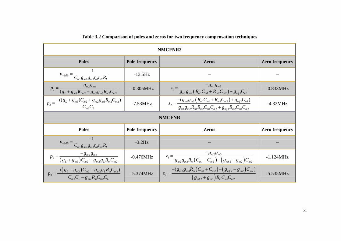
51
Table 3.2 Comparison of poles and zeros for two frequency compensation techniques
NMCFNR2
Poles Pole frequency Zeros Zero frequency
3
1 2 3 1 2
1dB
m m m o o L
pC g g r r R
-13.5Hz − −
2 32
3 2 2 3 2 2( )
m m
L m m m m m m
g gp
g g C g g R C
- 0.305MHz
1 2
1
1 2 1 1 2 2 1 1
m m
m m m m m m mf m
g gz
g g R C R C g C
-0.833MHz
3 2 2 3 2 23
2
(( ) )L m m m m m m
m L
g g C g g R Cp
C C
-7.53MHz
1 2 1 1 2 2 1 1
2
1 2 1 2 1 2 1 2 1 2
( )m m m m m m mf m
m m m m m m mf m m m
g g R C R C g Cz
g g R R C C g R C C
-4.32MHz
NMCFNR
Poles Pole frequency Zeros Zero frequency
3
1 2 3 1 2
1dB
m m m o o L
pC g g r r R
-3.2Hz − −
2 3
2
3 2 2 2
m m
L m m m L m m
g gp
g g C g g R C
-0.476MHz
2 3
1
2 3 1 2 2 2 2
m m
m m m m m mf m m
g gz
g g R C C g g C
-1.124MHz
3 2 2 2
3
2 2 2
( )L m m m L m m
m L m m m L
g g C g g R Cp
C C g R C C
-5.374MHz
2 3 1 2 2 2 2
2
2 3 1 2
( )m m m m m mf m m
mf m m m m
g g R C C g g Cz
g g R C C
-5.535MHz
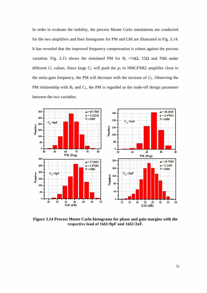
52
In order to evaluate the stability, the process Monte Carlo simulations are conducted
for the two amplifiers and their histograms for PM and GM are illustrated in Fig. 3.14.
It has revealed that the improved frequency compensation is robust against the process
variation. Fig. 3.15 shows the simulated PM for RL =16Ω, 32Ω and 50Ω under
different CL values. Since large CL will push the p3 in NMCFNR2 amplifier close to
the unity-gain frequency, the PM will decrease with the increase of CL. Observing the
PM relationship with RL and CL, the PM is regarded as the trade-off design parameter
between the two variables.
Figure 3.14 Process Monte Carlo histograms for phase and gain margins with the
respective load of 16Ω//0pF and 16Ω//2nF.

53
0.0 500.0p 1.0n 1.5n 2.0n
10
20
30
40
50
60
70
80
RL=32
RL=50
Ph
ase
Margin
(D
eg)
CL(F)
RL=16
Figure 3.15 Simulated PM for RL=16Ω, 32Ω and 50Ω when sweeping the CL from
0pF to 2nF.
A headphone load will display both inductive and capacitive effect in a form of
resonant circuit which is reported as the approximated headphone load model [69]. In
this design, the impedance of 16Ω headphone model, having a resonant frequency of
2MHz, is adopted. The circuit model is shown in Fig. 3.16, with RA=5Ω, CL=332pF,
RL=17Ω, RB=340Ω, LL=20µH. To assess the stability, Fig. 3.17 depicts the simulated
open-loop gain and phase responses of amplifier with the approximated headphone
load, yielding GBW=6.7MHz, PM=41º and GM=9.5dB. This amplifier system is
considered stable because of having adequate GM. Of particular interest, the GBW is
enhanced due to the additional high-frequency zero caused by the inductive effect. To
further improve the PM by 10º at the expense of silicon area, a 20pF can be added
across the feedback resistor R2 in Fig. 3.1.

54
CL
RL
LL
RB
RA
Figure 3.16 The approximated headphone impedance model [69].
100m 1 10 100 1k 10k 100k 1M 10M 100M
-90
0
90
180
-40
0
40
80
120
Ph
ase
(D
eg
)
Frequency (Hz)
Ga
in (
dB
)
Figure 3.17 The simulated open-loop gain and phase for headphone amplifier
using the approximated headphone impedance load model.
The simulation result of NMCFNR2 amplifier correlates well with the theory. Due to
the relaxation in the design tradeoff, this explains why the GBW can be enhanced with
the improved scheme.

55
3.3. Transistor Level Realization of Headphone Amplifier
Fig. 3.18 depicts the simplified schematic of the proposed class-AB headphone
amplifier circuit with the balanced offset compensation circuit for the differential input
stage and the channel-length modulation (CLM) reduced class-AB bias generation
circuit for the push-pull output stage. This is a three-stage amplifier topology which
employs an improved compensation topology, called NMCFNR2 to drive a parallel
resistive and capacitive load. As mentioned above, the topology works along with the
offset calibration system to reduce the offset arising from the difference amplifier
topology. The use of CLM-reduced bias generation circuit offers an improved
quiescent bias control in the class-AB push-pull output stage with respect to that of the
conventional bias circuit. The employment of improved frequency compensation in the
APA design permits low quiescent power consumption whilst yielding adequate gain-
bandwidth metric and small compensation capacitors for audio applications in the
context of stability against very low resistive load drive. The proposed three-stage
amplifier is mainly made up of a folded-cascode differential input stage, a non-
inverting gain stage and a push-pull output stage. The detailed design considerations of
each stage are discussed in the following sub-sections.
3.3.1. Realization of Input Stage of Headphone Amplifier
The first stage is realized with folded-cascode topology, which is formed by transistors
M1-M11. An input stage determines the performance of the APA in many aspects,
including DC gain, input-referred offset, GBW, input-referred noise and so forth.

56
Vin+Vin-
VDD
VSS
M1
M3 M4
M6 M7
VOUT
M5
VBP2
VBN2
VBN1
M14 M15
M12
M17
VBP1
Differential Input Stage Non-inverting Gain Stage Output Stage
M2
M10 M11
M9M8
M18
M19
Rm2
Rm2
Cm2
Cm2
Cm1
RL CL
IB1
IB3
IB1
IB2
Digitally Programmable
Current Source
YX
Balanced Offset Compensation Current DAC
M16
M13
Rm1
gmf1
CLM-reduced
class-AB bias
generation circuit
Figure 3.18 The simplified schematic of the APA with embodiment of proposed balanced offset compensation circuit and CLM-
reduced class-AB bias generation circuit.

57
Since the first stage is one of the major stages to contribute high DC gain in the APA,
the equivalent trans-conductance (gm1) should be maximized whilst the equivalent
output impedance of first stage should be made high. For obtaining high current
efficiency of gm, the input transistors M1 and M2 are biased in the sub-threshold region
with large aspect ratio. The folded cascode topology can enhance the equivalent output
resistance of the first stage. The DC gain of first stage can be as high as 90dB.
The input-referred offset voltage and noise of an amplifier are dictated by the first gain
stage. Therefore, the size of the differential input transistor pair is made large for
biasing in subthreshold region whereas the respective transconductance for current
source pair transistors, M3 and M4 and the mirror active load transistors, M10 and M11,
is made small through the use of longer channel length. Not only does this arrangement
increase the device matching characteristics, it also reduces both thermal and flicker
noise. The noise analysis of the headphone amplifier will be presented in details in the
following section. The use of folded-cascode topology provides high output swing as
well as high input common-mode range. The bias voltages VBP1, VBP2, VBN1 and VBN2
are generated by the simple low-voltage cascode bias generators (not shown in Fig.
3.18).
3.3.2. Realization of Second Stage of Headphone Amplifier
The second gain stage of APA is made up of transistors M12-M17, which realizes a
dual-input non-inverting gain stage with current mirror active load, M14 and M15, as
shown in Fig. 3.19. The transistors M16 and M17 form the floating voltage biasing
source. They are of great importance for biasing the output stage. In this circuit, they
will be used to bias the CLM-reduced class-AB bias generation circuit. The gain of this

58
second stage is much lower than that of the first stage since it is a common source
amplifier without employing cascode topology to enhance the output impedance.
Consider the output voltage of APA increases from 0V, the source-gate voltage of
PMOS output transistor increases continuously. At this juncture, ID,M16 drops since the
its source voltage decreases with the gate voltage being constant. As illustrated in Fig.
3.19, when the transistor M16 enters the cut-off region, all the biasing current of M13
will be steered towards the current flow in the floating biasing transistor M17. This
leads to increase its source voltage because the gate voltage is kept constant by the
CLM-reduced bias generation circuit. As a result, the gate-source voltage of NMOS
output transistor significantly drops to almost cutting off state. The similar operation
goes for the floating biasing transistor M16 for the negative going output voltage of
APA.
M14 M15
M12
M13
M17M16VP VN
Non-inverting
Gain Stage
V1
VBP4
VDD
VSS
I2
ID17 = I2ID16 = 0
I2
Figure 3.19 Illustration of biasing current flow in one of floating biasing transistors
when the output voltage of APA goes positive.
59
3.3.3. Realization of Output Stage of Headphone Amplifier
The transistors M18 and M19 realize the third stage gm3 as shown in Fig. 3.18. Since the
amplifier is required to drive very small resistive load and large capacitive load, the
aspect ratio for M18 and M19 should be made big to provide enough current for
sourcing to or sinking from the load. The quiescent current of output transistors are
determined by the DC conditions of the previously mentioned CLM-reduced bias
generation circuit. If each current of M16 or M17 is designed with half of that in the
current source transistor M13, the respective gate voltage of the output transistor can be
well-defined. Hence, their corresponding quiescent current is under good control. In
order to implement a low-power amplifier design, the quiescent current of output
transistors needs to be optimised to balance the quiescent power and the distortion.
Since the mobility of electrons is about three times of the holes in 65-nm CMOS
technology, the width of p-type output transistor is set to be three times of the n-type
output transistor for a symmetrical output swing. The large transistor size of the third
stage results in large parasitic capacitance in the output node of second stage. This
implies that the non-dominant pole arising from the second stage may be pushed
towards low frequency. This may jeopardize the frequency compensation of amplifier.
Therefore, the smallest channel length of the output stage is commonly utilized to
minimize the silicon area as well as the parasitic capacitances. However, the price paid
for small channel length transistors is that of the increase of channel length modulation
effect, causing the inaccuracy of the biasing current in the output transistors. The
employment of CLM-reduced bias generation circuit will relax the drawback.
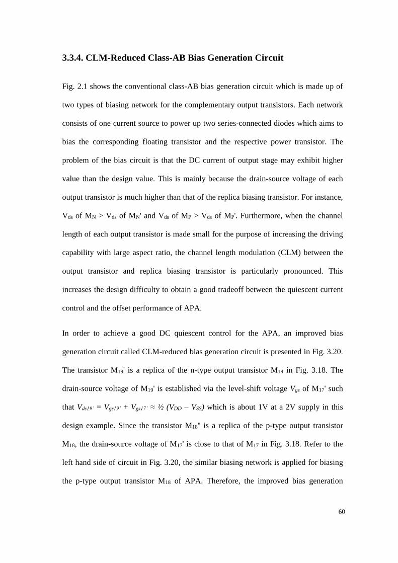
60
3.3.4. CLM-Reduced Class-AB Bias Generation Circuit
Fig. 2.1 shows the conventional class-AB bias generation circuit which is made up of
two types of biasing network for the complementary output transistors. Each network
consists of one current source to power up two series-connected diodes which aims to
bias the corresponding floating transistor and the respective power transistor. The
problem of the bias circuit is that the DC current of output stage may exhibit higher
value than the design value. This is mainly because the drain-source voltage of each
output transistor is much higher than that of the replica biasing transistor. For instance,
Vds of MN > Vds of MN' and Vds of MP > Vds of MP'. Furthermore, when the channel
length of each output transistor is made small for the purpose of increasing the driving
capability with large aspect ratio, the channel length modulation (CLM) between the
output transistor and replica biasing transistor is particularly pronounced. This
increases the design difficulty to obtain a good tradeoff between the quiescent current
control and the offset performance of APA.
In order to achieve a good DC quiescent control for the APA, an improved bias
generation circuit called CLM-reduced bias generation circuit is presented in Fig. 3.20.
The transistor M19' is a replica of the n-type output transistor M19 in Fig. 3.18. The
drain-source voltage of M19' is established via the level-shift voltage Vgs of M17' such
that Vds19’ = Vgs19’ + Vgs17’ ≈ ½ (VDD – VSS) which is about 1V at a 2V supply in this
design example. Since the transistor M18'' is a replica of the p-type output transistor
M18, the drain-source voltage of M17' is close to that of M17 in Fig. 3.18. Refer to the
left hand side of circuit in Fig. 3.20, the similar biasing network is applied for biasing
the p-type output transistor M18 of APA. Therefore, the improved bias generation
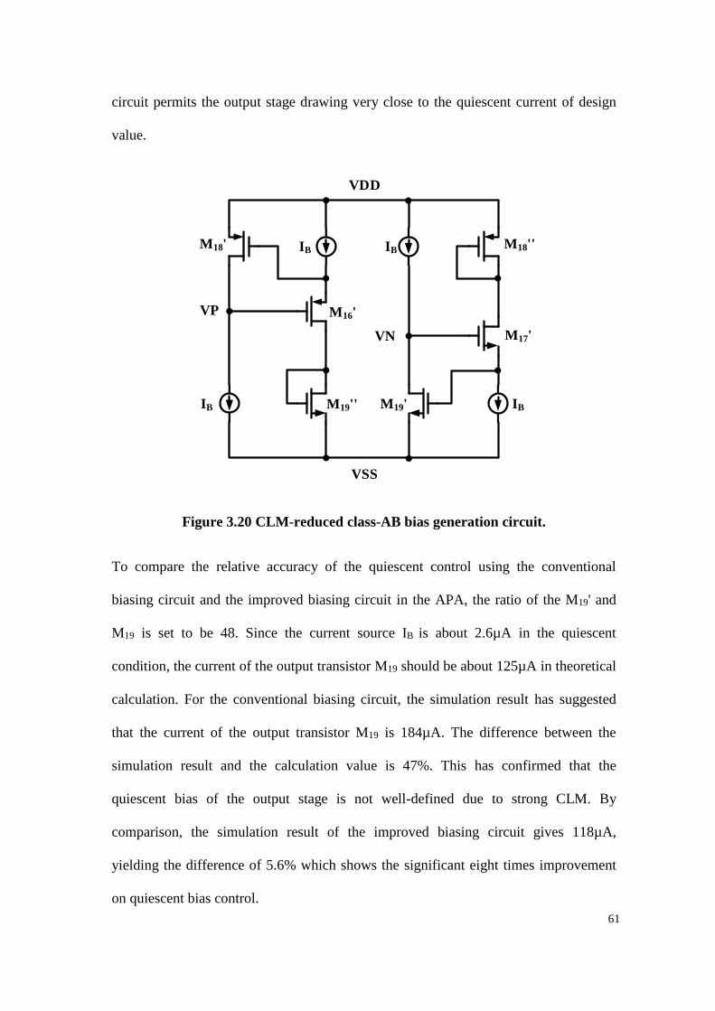
61
circuit permits the output stage drawing very close to the quiescent current of design
value.
IB
IB IB
IBM19'
M17'
M18'
M16'
VDD
VSS
M18''
M19''
VP
VN
Figure 3.20 CLM-reduced class-AB bias generation circuit.
To compare the relative accuracy of the quiescent control using the conventional
biasing circuit and the improved biasing circuit in the APA, the ratio of the M19' and
M19 is set to be 48. Since the current source IB is about 2.6µA in the quiescent
condition, the current of the output transistor M19 should be about 125µA in theoretical
calculation. For the conventional biasing circuit, the simulation result has suggested
that the current of the output transistor M19 is 184µA. The difference between the
simulation result and the calculation value is 47%. This has confirmed that the
quiescent bias of the output stage is not well-defined due to strong CLM. By
comparison, the simulation result of the improved biasing circuit gives 118µA,
yielding the difference of 5.6% which shows the significant eight times improvement
on quiescent bias control.

62
For further illustration of the performance of two bias generation circuits, the Monte
Carlo simulation results are conducted. The offset current is defined as the current
difference between the output stage simulation results and the theoretical design values
on the basis of the transistor size ratio of the output transistors and their replica biasing
transistors.
-200.0μ-100.0μ 0.0 100.0μ 200.0μ 300.0μ 400.0μ 500.0μ
0
50
100
150
200
250
300
350
400 mu=21.73u
sd=80.51u
N=1000
Nu
mb
er
Offset Current (A)
Figure 3.21 Monte Carlo simulation results for offset current using the CLM-
reduced bias generation circuit.
-100.0μ 0.0 100.0μ 200.0μ 300.0μ 400.0μ 500.0μ
0
50
100
150
200
250
300
350
400 mu=82.25u
sd=79.07u
N=1000
Nu
mb
er
Offset Current (A)
Figure 3.22 Monte Carlo simulation results for offset current using the
conventional bias generation circuit.

63
Fig. 3.21 and Fig. 3.22 show the Monte Carlo simulation results of the offset current
for the two bias generation circuits. The biasing currents for each bias generation
circuit are designed with the same values. The offset current reveals the actual
variation of the output stage biasing current with respect to the target design value.
From the simulation results, it can be seen that the mean value of the offset current for
the proposed CLM-reduced bias generation circuit is 21µA whilst the standard
deviation is about 78µA. In comparison, the conventional bias generation circuit
contributes similar value of standard deviation but having the mean value of 82µA,
which is about 4 times larger than that of the improved bias circuit. This has confirmed
that the APAs are subject to higher variation of bias current in the output transistor
when using the conventional bias generation circuit. On the contrary, the CLM-
reduced bias circuit offers relative lower sensitivity to the DC quiescent current
variation.
The offset current in the proposed CLM-reduced bias generation circuit mainly comes
from the threshold voltage variation and gate-source mismatch between the power
transistors and the corresponding replica biasing transistors. Compared to the
conventional bias generation circuit, the proposed CLM-reduced bias generation
circuit provides better drain-source voltage matching, thus reducing the offset current.
In general, the APA should provide the immunity against the supply variation. The
same goes for the bias generation circuit. For the intentional variation of ±10% in the
APA powered by the ±1V supplies, the Monte Carlo simulation results have indicated
that the standard deviation of both the bias generation circuits do not change
significantly. However, the mean value of the bias current of conventional bias circuit
changes to about 100µA. This is about 4 times larger than that of CLM-reduced bias

64
circuit which has a mean value of 28µA. For this observation, it can conclude that the
CLM-reduced bias generation circuit is relatively insensitive to the change of power
supply voltage.
In the context of delivering higher power output for the APA, the supply voltage needs
to be increased. For instance, the supply voltage is increased from ±1V to ±1.5V. The
bias generation circuit should be able to support higher supply APA design. This is
achieved by adding two diode-connected transistors M20 and M21 for additional voltage
level shift in the bias generation circuit. Fig. 3.23 depicts the simplified schematic of
APA having a modified CLM-reduced bias generation circuit dedicated to ±1.5V
supply. Since the CLM-reduced bias generation circuit can still provide similar level of
drain-source voltages for the respective output transistor and the corresponding replica
biasing transistors, the quiescent current of output stage can be well-defined. The
similar change will be applied for the conventional bias circuit powered by ±1.5V
supply for comparative study.
VDD
VSS
VOUT
M15
M13
M17
M16
Output Stage
M18
M19
Rm2
Rm2
Cm2
Cm2
IB
IB IB
IBM19'
M17'
M18'
M16'
CLM-Reduced Class-AB Bias Generation
Circuit
VB1
VIN2
IB
M16'
IB
M17'
M18''M18''
M19'' M19''
M20M20
M21
M21
Level Shifter for Output Stage
RL CL
Figure 3.23 The schematic of APA with high-voltage CLM-reduced bias
generation circuit in ±1.5V supply.

65
Fig. 3.24 and Fig. 3.25 present the Monte Carlo simulation results of the offset current
for the two bias generation circuits in ±1.5V supply. It can be found that the mean
offset current value of conventional bias circuit is double when the supply is increased
from ±1V to ±1.5V. It is also about 8 times larger than that of the improved bias circuit.
On the other hand, the quiescent control in the improved circuit remains the same
regardless of the supply being increased from ±1V to ±1.5V. The improved bias circuit
displays robust characteristic in APA design.
-200.0μ-100.0μ 0.0 100.0μ 200.0μ 300.0μ 400.0μ 500.0μ
0
50
100
150
200
250
300
350
400 mu=19.26u
sd=76.02u
N=1000
Nu
mb
er
Offset Current (A)
Figure 3.24 Monte Carlo simulation for offset current using the high-voltage
CLM-reduced bias generation circuit with ±1.5V supply.

66
-200.0μ-100.0μ 0.0 100.0μ 200.0μ 300.0μ 400.0μ 500.0μ
0
50
100
150
200
250
300
350
400 mu=161.30u
sd=80.90u
N=1000
Nu
mb
er
Offset Current (A)
Figure 3.25 Monte Carlo simulation for offset current using the conventional
high-voltage bias generation circuit with ±1.5V supply.
-5.00m -2.50m 0.00 2.50m 5.00m
400.0μ
600.0μ
800.0μ
1.0m
CLM-reduced Biasing Circuit
Tota
l Q
uie
scen
t P
ow
er (
W)
Input Offset (V)
Conventional Biasing Circuit
Figure 3.26 The total quiescent power versus the input offset of amplifier under
two different biasing circuits.
Fig. 3.26 shows the plot of the quiescent power against the input-referred offset with
two types of bias generation circuit. It can be seen that the total quiescent power in
both circuits will increase with the increase of offset voltage. Table 3.3 shows the

67
value of the total quiescent power with the change of input-referred offset for two
different bias generation circuits.
Table 3.3 Comparison of APAs with the conventional biasing circuit and the
improved biasing circuit for the push-pull output stage.
Parameters VOFFSET
(mV)
Total
Quiescent
Power (mW)
Relative Quiescent
Power Error
(with respect to the 0mV)
Conventional
Bias
Generation
Circuit
0 mV 0.5505 mW + 28.17%
1 mV 0.5795 mW + 34.92%
2 mV 0.6565 mW + 52.85%
3 mV 0.7566 mW + 76.16%
4 mV 0.8673 mW +101.9%
5 mV 0.9831 mW +128.9%
CLM-
Reduced
Bias
Generation
Circuit
0 mV 0.4295 mW + 0%
1 mV 0.4811 mW + 12.01%
2 mV 0.5798 mW + 34.99%
3 mV 0.6931 mW + 61.37%
4 mV 0.8119 mW + 89.03%
5 mV 0.9330 mW + 117.2%
For APA with the CLM-reduced bias generation circuit at ideal zero offset condition,
the total quiescent power consumption is about 0.43mW. With the employment of the
proposed calibration system for non-ideal offset nulling, the absolute offset value
becomes less than 85µV which accounts to the total quiescent power increase by only
0.23%. However, for a class-AB APA with the conventional bias generation circuit
without the offset nulling system at ideal zero offset condition, the total quiescent
power will increase by 28.17%. The CLM-reduced bias generation circuit is effective
for APA with the offset voltage less than 3mV. With the increase of input offset

68
voltage, the mismatch-induced current will be quite large and the effect of CLM-
reduced bias generation circuit on quiescent power consumption will be smaller.
3.3.5. Bias Generation and Start-up Circuit
M21 M22
M23
M25 M26
M27
M24
R
M28
CS
VDD
VSS
VBP1
VBN3
Figure 3.27 Constant transconductance bias circuit with startup circuit.
The biasing voltage in the proposed amplifier in Fig. 3.18 is generated by the constant
transconductance bias circuit shown in Fig. 3.27. In this circuit, the DC current in M25
and M26 are the same but the transistor channel width has a ratio of W25:W26 = 1:4. The
gate-source voltage of M25 and M26 are related by
, 25 , 26 , 26gs M gs M D MV V I R (3.7)
69
Since M25 and M26 have the same threshold voltage, the equation can be rewritten as
, 25 , 26
, 26
25 26
2 2D M D M
D M
n n
M M
I II R
W WK K
L L
(3.8)
With the identical DC current in M25 and M26 and the transistor ratio of 1:4, the
equation can be simplified as
, 25
25
1
*2 n D M
M
RW
K IL
(3.9)
Due to , 25 , 25
25
2 *m M n D M
M
Wg K I
L
. it turns out that
, 25 1/m Mg R . Therefore, the
biasing DC current ID,M25 is well defined at a constant temperature. In order to
investigate the temperature dependence of biasing current on the temperature, the
simulation is conducted.
-60 -40 -20 0 20 40 60 80 100
4.6μ
4.8μ
5.0μ
5.2μ
5.4μ
Bia
sin
g C
urr
en
t (A
)
Temperature (oC)
Figure 3.28 The temperature variation of DC current for bias circuit.

70
Fig. 3.28 shows the simulated results for the change of biasing current with
temperature. It can be observed that the biasing current continuously increases with
temperature until reaching the saturation at 70 ºC. This can be explained by the
temperature dependence of the resistor and transistor parameters in the relationship as
follows:
2
25
1
2 ( )( )D
n ox
M
IW
µ C R TL
T
(3.10)
Equation (3.10) shows that the biasing current depends on the process constant, the
design parameter, the temperature-dependent carrier mobility and the thermal behavior
of resistor. With the increase of temperature, the lattice scattering will be increased and
the electron mobility will be lower. On the other hand, for the N-well resistor adopted
in the amplifier, its value will increase with the temperature. As a result, there is a
slight partial cancellation of thermal effect between the two parameters. The simulated
results have revealed that the dependence of biasing current on temperature is
dominated by the electron mobility in the temperature range of -40 ºC to 70 ºC, in
which the biasing current increases with temperature. For the temperature range of 70
ºC to 90 ºC, the biasing current is almost constant with the change of temperature,
which indicates that both the thermal effects between the electron mobility and the
resistor are comparable. Of particularly interest, the biasing current stays fairly
constant. Finally, other device parameters, such as threshold voltage mismatch and DC
current mismatch may also influence the bias current variation with temperature, but
they are not the main contributing factors for the thermal effect on the biasing current.

71
3.4. Noise Analysis of Proposed Headphone Amplifier
The headphone amplifier is conducted with the noise analysis. The total input-referred
noise of a CMOS headphone amplifier is mainly dominated by the flicker and thermal
noise in the first stage. The noise in the second stage and output stage can be ignored
due to the high gain of first stage. For the APA, the flicker noise is the dominant noise
source, and hence the thermal noise is neglected.
Vin+Vin-
VDD
VSS
M1
M3 M4
M6 M7
M5
VBP2
VBN2
VBN1
VBP1
M2
M10 M11
M9M8
IB1
IB3
IB1
IB2
Digitally Programmable
Current Source
YX
Balanced Offset Compensation Current DAC
Figure 3.29 The folded-cascode stage of the proposed headphone amplifier.
Fig. 3.29 shows the folded-cascode stage of headphone amplifier. The p-channel input
pairs are adopted for low noise design because the flicker noise coefficient, KF, of
PMOS transistor is smaller than that of NMOS [70]. The flicker noise is inversely
proportional to the frequency and transistor area. As mentioned in the previous section,
the gate area of input pair and the active loads are made large. In addition, the balanced
offset compensation current sources IB1 ~ IB4 will also contribute to the input-referred
noise since they directly inject current into the input stage. Nevertheless, since the DC
72
current of the four current sources are injected at the low impedance nodes in the first
stage, the noise contribution of these current sources becomes negligible. As a result,
the total input-referred noise of the amplifier mainly depends on the transistor M1- M4,
M10 and M11 whilst the noise contribution of cascade transistors is very small to be
ignored.
Based on the Gray and Meyer noise model [71] and neglecting the thermal noise, the
total noise current of a single transistor is approximated as
2 2
t F m
OX
i K g
f C WLf
(3.11)
where Δf is the bandwidth and other symbols have their usual meanings. Therefore, the
equivalent noise voltage at the gate of the single transistor can be written in a form of
2
eq F
OX
V K
f C WLf
(3.12)
Regarding the amplifier design in [71], the input-referred noise voltage of amplifier are
determined by the transconductance ratio between the input pair and the active load
together with the process and design parameters. In the headphone amplifier, ID3 =
5ID10 and ID1 = 4ID10. According to the folded-cascode noise analysis in [70], the
equivalent input-referred noise of amplifier can be approximated as follows:
2 2 2_ 10 3
2 2
1 1 10 10 1 3 3 1
2( )eq APA Fp Fp m Fn m
OX OX m OX m
V K K g K g
f C W L f C W L f g C W L f g
(3.13)
Substituting gmi by 2 ii OXi Di
i
Wµ C I
L, the equation (3.13) can be simplified as

73
2
_ 11
2 2
1 1 10 3
2 51( )
4 4
eq APA Fp Fn n
OX Fp p
V K K LL
f C W f L L K L
(3.14)
In general, the mobility of electron is about three times that of holes whereas KFn is
larger than KFp. In order to find the appropriate input pair channel length and simplify
the analysis, one can ignore the flicker noise contributed by M10 and M11 due to L1 <<
L10. From the equation (3.14), there exists an optimised channel length for input pair
such that the amplifier can offer the minimum input-referred noise with respective to
the given design parameters.
0.2 0.4 0.6 0.8 1.0 1.2
120.00n
121.20n
122.40n
123.60n
124.80n
Inp
ut-
refe
rred
No
ise @
1k
Hz
(V/√
Hz)
Channel Length (m)
Figure 3.30 Input-referred noise of amplifier versus the input pair channel length.
Fig. 3.30 shows the simulated input-referred noise of amplifier with different input pair
channel length. It shows that the optimized channel length for the input pair is about
0.5µm to 0.6µm. In order to minimize the parasitic capacitances of the input pair, the
channel length of 0.5µm is used in the headphone amplifier.

74
Chapter 4 Measured Results and Discussions
Implemented and fabricated in 65-nm CMOS technology, the micrograph and Cadence
layout drawing of the headphone amplifier is shown in Fig. 4.1 and Fig. 4.2,
respectively. The total active area of the circuit is about 0.15mm2 (480µm×320µm), in
which the digital blocks and the power transistors contribute to about two thirds. Since
the power transistors sink or source large current, they are placed close to the pad
whilst far away from the core amplifier. In order to confirm the APA’s performance
from the design, the crucial parameters of headphone amplifiers are measured, which
includes input-referred offset, THD+N, SNR, PSRR and pulse response.
CC1 & CC2
Gm3P
Gm3N
480µm
32
0µ
m
Power PMOS
Power NMOS
Bias Generator
Core Amplifier
R1-R4
Digital-Assisted Offset
Calibration Circuit
Figure 4.1 The micrograph of the proposed headphone amplifier in 65-nm CMOS.

75
Figure 4.2 The Cadence layout drawing of the proposed headphone amplifier in
UMC 65-nm CMOS.
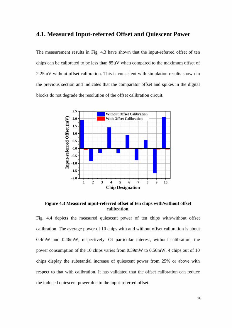
76
4.1. Measured Input-referred Offset and Quiescent Power
The measurement results in Fig. 4.3 have shown that the input-referred offset of ten
chips can be calibrated to be less than 85µV when compared to the maximum offset of
2.25mV without offset calibration. This is consistent with simulation results shown in
the previous section and indicates that the comparator offset and spikes in the digital
blocks do not degrade the resolution of the offset calibration circuit.
1 2 3 4 5 6 7 8 9 10-2.0
-1.5
-1.0
-0.5
0.0
0.5
1.0
1.5
2.0
2.5
Inp
ut-
refe
rred
Off
set
(mV
)
Chip Designation
Without Offset Calibration
With Offset Calibration
Figure 4.3 Measured input-referred offset of ten chips with/without offset
calibration.
Fig. 4.4 depicts the measured quiescent power of ten chips with/without offset
calibration. The average power of 10 chips with and without offset calibration is about
0.4mW and 0.46mW, respectively. Of particular interest, without calibration, the
power consumption of the 10 chips varies from 0.39mW to 0.56mW. 4 chips out of 10
chips display the substantial increase of quiescent power from 25% or above with
respect to that with calibration. It has validated that the offset calibration can reduce
the induced quiescent power due to the input-referred offset.

77
1 2 3 4 5 6 7 8 9 10
400
450
500
550
Qu
iesc
net
Pow
er
Con
sum
pti
on
(
W)
Chip Designation
Without Offset Calibration
With Offset Calibration
Figure 4.4 Measured quiescent power consumption of ten chips with/without
offset calibration.

78
4.2. Measured THD+N and SNR Results
The test chips are measured by the Stanford Research System (SRS) SR1 audio
analyzer. Fig. 4.5 shows the FFT output signal of the amplifier with the 1 kHz
sinusoidal input signal of 1.5Vpp. It is noted that 0dBr in the vertical axis represents
1Vrms (0dB). All the harmonics are less than -100dB. The headphone amplifier has
achieved -91dB THD at peak load power. Finally, the A-weighted THD+N and SNR at
peak load power in the 20Hz-20kHz bandwidth are measured with -89dB and 93.5dB,
respectively.
Figure 4.5 Measured output signal in FFT with the 1.5VPP 1 kHz input sinusoidal
wave.
Fig. 4.6 shows the measured A-weighted THD+N versus the output amplitude for 1
kHz input signal. It shows that the THD+N for the headphone amplifier decreases with
the input signal level until 1.5Vpp, which confirms that the peak output voltage is
1.5Vpp. The THD+N for small signal input is high because the SNR will drop for low
level input signal. With the increase of input signal, the SNR will increase, thus
resulting in lower THD+N. Fig. 4.7 shows the A-weighted THD+N having different
signal frequencies at peak load power. For the low frequency signal, the flicker noise
of amplifier deteriorates the SNR, but displaying better linearity. The combined effect

79
results in lower THD+N at low frequencies. On the other hand, with increasing the
input signal frequency, the distortion increases due to the drop of open-loop gain.
Finally, the high-frequency harmonics in the audio band decreases with the increasing
frequency, thus contributing to the improved THD+N if the distortion does not
significantly degrade the SNR [3], [72].
Figure 4.6 Measured THD+N versus output amplitude for 1 kHz input signal.
Figure 4.7 Measured THD+N versus signal frequency with 1.5VPP input sine-wave
signal.

80
4.3. Measured PSRR Results
Fig. 4.8 shows the FFT plot of the amplifier’s output in response to the 700mVPP 217
Hz input signal which is applied on the positive power supply of amplifier. The
measured PSRR+ can be obtained with the ratio of the input and output AC signal at
217 Hz, which has the value of 84dB. Similar measurement is also conducted on the
negative power supply of amplifier. Fig. 4.9 shows that the PSRR- is 105dB at 217 Hz.
PSRR@217Hz
=84dB
VOUT
VDD
Figure 4.8 Measured PSRR+ at 217Hz with 700mVPP on the 1V positive supply.
PSRR@217Hz
=105dB
VOUT
VSS
Figure 4.9 Measured PSRR- at 217Hz with 700mVPP on the 1V negative supply.

81
4.4. Measured Pulse Response
The simulation results for the frequency response in previous section have indicated
that the proposed APA can drive a capacitive load range of 0-2nF. Fig. 4.10 shows the
measurement result of a rectangular input waveforms of 50kHz and 500mV with the
load of 1nF//16Ω. In order to verify the driving capability of the proposed headphone
amplifier, the large-signal pulse responses of the amplifier at different capacitive loads
in parallel with the resistive load are compared and shown in Fig. 4.11. There is no
significant peaking or ringing in the measured pulse response. This means that the
amplifier can drive the maximum load of 2nF//16Ω. The measured results also show
that the proposed APA can achieve the slew rate of 1.1V/µs.
Figure 4.10 Measurement result of a rectangular input waveforms of 50kHz and
500mV with the load of 1nF//16Ω.

82
-0.4
0.0
0.4
-0.4
0.0
0.4
-0.4
0.0
0.4
-0.4
0.0
0.4
-40.0μ -20.0μ 0.0 20.0μ 40.0μ
-0.4
0.0
0.4
Input
16//2nF
16//1nF
16//8pF
16//300pF
Time (s)
Inp
ut
an
d O
utp
ut
Sig
nal
(V)
Figure 4.11 The pulse response of the headphone amplifier with the respective
load of 16Ω//8pF, 16Ω//300pF, 16Ω//1nF and 16Ω//2nF.

83
4.5. Performance Comparison
Table 4.1 shows the performance comparison of the headphone amplifier with the
recently-published state-of-the-art works. Among the topologies, the proposed
amplifier consumes the quiescent power of 0.4mW and requires a total compensation
capacitance of 8.5pF, which are considered as the lowest values. The peak THD+N is -
89dB, which is higher most of the recently-published state-of-the-art works. The PSRR
is 84dB and it is comparable to [5] and the product in [12]. The work in [8] is powered
by LDO so that it can provide a high PSRR of 110dB. At the same juncture, it also
provides the comparable performance metrics such as A-weighted SNR, GBW and
slew rate. The capacitive load range is 0-2nF, which is lower than [2], [3], [5] but
higher than the product in [12]. The FOM1, which is defined as the ratio of the peak
power over the quiescent power, is obtained as 87.9. Another figure of merit FOM2,
which is defined as the ratio of FOM1 over THD+N in percentage, is compared. Both
FOM1 and FOM2 have displayed the highest values among those of the reported
works, demonstrating the effectiveness of two circuit techniques in the low-quiescent
high-performance headphone amplifier design.

84
Table 4.1 Performance comparison of reported prior-art results.
Parameters
[12]
Maxim
2002
[2]
ESSCIRC
2006
[3]
JSSC
2009
[5]
TCASII
2012
[6]
VLSIC
2012
[7]
JSSC
2012
[8]
JSSC
2014
This work
Process (nm) NA 65 130 500 40 130 40 65
Supply (V) 3.0 2.5 1.2/2.0 3.0 1.1/1.8 1.5 3.1/4.5 2.0
Resistive load (Ω) 16 16 16 16 16 16 16 16
Capacitive Load (F) 0-300p 0-12n 1pF-22n 10p-5n NA NA NA 0-2n
Gain (dB) 60 NA NA 51.5 NA NA NA 113
Phase Margin (º) 40 NA >45 72 NA NA NA > 45
GBW (MHz) 2.5 NA 4 1.23 NA NA NA 1.78
PSRR@ 217Hz (dB) 90 NA NA 70 92 NA 110* 84
Slew Rate (V/µs) 0.8 NA 0.4 1.2 NA NA NA 1.1
Quiescent Power (mW) 12.0 12.5 1.2 1.43 5.2 1.5 3.8 0.4
Output Voltage (VPP) 2.5 1.85 1.6 2.45 1.41 2.5 3.24 1.5
A-weighted SNR (dB) 95 NA 92 79.9 100 98 100 93.5
Peak THD+N (dB) -90 -68 -84 -77.9 -91 -72 -84 -89
Total Compensation
Capacitance (pF) NA 35 14 16.3 NA NA NA 8.5
FOM1 & 8.1 4.3 33.3 65.8 6 65.3 43.4 87.9
FOM2# 2561 108 5278 5167 2129 2600 6878 24774
*: Powered by LDO regulator and charge pump &: FOM1=(Peak load power )/(Quiescent power) #: FOM2=(Peak load power )/(Quiescent power*THD+N (%))
85
Chapter 5 Conclusions and Future Works
5.1. Conclusions
A low-offset low-quiescent power class-AB headphone amplifier has been proposed
and discussed together with the measurement results and the detailed analysis in this
thesis. Two key low-quiescent design techniques for headphone amplifier have been
introduced.
Firstly, the digitally-assisted offset calibration circuit architecture is able to reduce the
mismatch-induced quiescent current caused by the input-referred offset of amplifier
without jeopardizing the PSRR as well as DC gain. The reduction of the input–referred
offset is achieved by digitally injecting current into the differential stage. Several
digital blocks are implemented to detect the offset value and control the injected
current. The low-offset technique is of great importance for power amplifier with the
decreasing of the device size in advanced CMOS technologies.
Secondly, the improved frequency compensation permits the amplifier to drive the
worst case load of 16Ω//2nF whilst sustaining good stability and providing good GBW
at low power. In the conventional frequency compensation topology, the assumption
about the third-stage gain is not applicable for headphone amplifier. Therefore, an
improved frequency compensation technique called NMCFNR2 that can be applied in
the power amplifier is introduced. Other performance metrics like PSRR, THD+N,
SNR are obtained with comparable performance. The amplifier outperforms the prior-
art works by achieving the best power-related FOM1 and power-(THD+N) related
FOM2, demonstrating the efficiency from quiescent state to full power state.

86
5.2. Future Work
For the power supplies of headphone amplifier, the voltage ripple of the switching
noise at 217Hz can be as high as several hundreds of mV. The proposed headphone
amplifier in this circuit has achieved positive PSRR of 84dB@217Hz, which is
comparable with other works. Nevertheless, the PSRR should be improved further to
minimise the impact of the supply noise over the output signal.
The offset calibration circuit proposed in this thesis has achieved relatively low offset.
However, the architecture of the calibration circuit produces glitches in the amplifier
output signal during the offset calibration period. Future work will focus on the glitch
reduction circuit techniques for the power-on start-up and the calibration circuit. In
addition, the successive approximation algorithm can be used in the circuit to generate
the approximate offset cancellation current after eight clock cycles. Not only does this
algorithm save the required offset calibration time, it also reduces the dynamic leakage
current.

87
Author’s Publication
1) F. Xiao and P. K. Chan, “A Performance-Aware Low-Quiescent Headphone
Amplifier in 65-nm CMOS” accepted by IEEE Journal of Solid-State Circuits,
2016

88
References
[1] R. Becker and W. H. Groeneweg, “An Audio Amplifier Providing Up to 1 Watt in
Standard Digital 90-nm CMOS,” IEEE J. Solid-State Circuits, vol. 41, no. 7, pp.
1648–1653, Jul. 2006.
[2] P. Bogner, H. Habibovic, and T. Hartig, “A high signal swing Class AB earpiece
amplifier in 65nm CMOS Technology,” in IEEE European Solid-State Circuits
Conference, 2006, pp. 372–375.
[3] V. Dhanasekaran, J. Silva-Martinez, and E. Sanchez-Sinenco, “Design of three-
stage class-AB 16Ω headphone driver capable of handling wide range of load
capacitance,” IEEE J. Solid-State Circuits, vol. 44, no. 6, pp. 1734–1744, 2009.
[4] W. H. Groeneweg, B. Pilloud, F. Neri, G. Notermans, M. Balucani, and M.
Helfenstein, “A class-AB/D audio power amplifier for mobile applications
integrated into a 2.5G/3G baseband processor,” IEEE Trans. Circuits Syst. I Regul.
Pap., vol. 57, no. 5, pp. 1003–1016, 2010.
[5] C. Mohan and P. M. Furth, “A 16-Ω Audio Amplifier With 93.8-mW Peak Load
Power and 1.43-mW Quiescent Power Consumption,” IEEE Trans. Circuits Syst.
II Express Briefs, vol. 59, no. 3, pp. 133–137, 2012.
[6] S. H. Wen and C. C. Yang, “A 5.2mW, 0.0016% THD up to 20kHz, ground-
referenced audio decoder with PSRR-enhanced class-AB 16Ω headphone
amplifiers,” in IEEE Symposium on VLSI Circuits, Digest of Technical Papers,
2012, pp. 20–21.
[7] X. Jiang, J. Song, J. Chen, V. Chandrasekar, S. Galal, F. Y. L. Cheung, D. Cheung,
and T. L. Brooks, “A low-power, high-fidelity stereo audio codec in 0.13 μm
CMOS,” IEEE J. Solid-State Circuits, vol. 47, no. 5, pp. 1221–1231, 2012.
[8] K. Abdelfattah, S. Galal, I. Mehr, A. J. Chen, C. Yu, M. Tjie, A. Tekin, X. Jiang,
and T. L. Brooks, “A 40 nm fully integrated 82 mW stereo headphone module for
mobile applications,” IEEE J. Solid-State Circuits, vol. 49, no. 8, pp. 1702–1714,
2014.
[9] J. Torres, A. Colli-Menchi, M. A. Rojas-Gonzalez, and E. Sanchez-Sinencio, “A
Low-Power High-PSRR Clock-Free Current-Controlled Class-D Audio Amplifier,”
IEEE J. Solid-State Circuits, vol. 46, no. 7, pp. 1553–1561, 2011.

89
[10] A. I. Colli-Menchi, J. Torres, and E. Sanchez-Sinencio, “A feed-forward power-
supply noise cancellation technique for single-ended class-D audio amplifiers,”
IEEE J. Solid-State Circuits, vol. 49, no. 3, pp. 718–728, 2014.
[11] X. Jiang, J. Song, D. Cheung, M. Wang, and S. K. Arunachalam, “Integrated
Class-D Audio Amplifier With 95% Efficiency and 105 dB SNR,” IEEE J. Solid-
State Circuits, vol. 49, no. 11, pp. 2387–2396, 2014.
[12] Maxim, “80mW , DirectDrive Stereo Headphone Driver with Shutdown,” 2002.
[Online]. Available: https://datasheets.maximintegrated.com/en/ds/MAX4410.pdf.
[13] T. Instrument, “80-mW DIRECTPATH TM STEREO HEADPHONE DRIVER,”
2008. [Online]. Available: http://www.ti.com.cn/cn/lit/ds/symlink/tpa4411.pdf.
[14] On Semiconductor, “NOCAP Advanced Stereo Headphone Amplifier,” 2010.
[Online]. Available: http://www.onsemi.cn/pub_link/Collateral/NCP2811-D.PDF.
[15]R. J. Wiegerink, E. Seevinck, and W. De Jager, “Offset cancelling circuit,” IEEE J.
Solid-State Circuits, vol. 24, no. 3, pp. 651–658, 1989.
[16]C. Azzolini and A. Boni, “A 1-V CMOS audio amplifier for low cost hearing aids,”
in IEEE International Conference on Electronics, Circuits and Systems, 2008, pp.
562–565.
[17] Y.-W. Chou, M.-W. Chien, S.-C. Chen, K.-H. Chen, Y.-H. Lin, T.-Y. Tsai, C.-C.
Huang, C.-C. Lee, Z. H. Tai, Y. H. Cheng, C. C. Tsai, H.-Y. Luo, S.-M. Wang, L.-
D. Chen, C.-C. Yang, and H. T. Hui, “A low THD clock-free Class-D audio
amplifier with an increased damping resistor and cross offset cancellation
technique,” in IEEE International Symposium on Circuits and Systems, 2014, pp.
2680–2683.
[18] S. Wong and C. Salama, “A switched differential op-amp with low offset and
reduced 1/f noise,” IEEE Trans. Circuits Syst., vol. 33, no. 11, 1986.
[19] I. G. Finvers, J. W. Haslett, and F. N. Trofimenkoff, “High temperature precision
amplifier,” IEEE J. Solid-State Circuits, vol. 30, no. 2, pp. 120–128, 1995.
[20] M. Sanduleanu, B. Nauta, and H. Wallinga, “Low-power low-voltage chopped
transconductance amplifier for noise and offset reduction,” IEEE Eur. Solid-State
Circuits Conf., pp. 13–16, 1997.
[21] A. Bakker, K. Thiele, and J. H. Huijsing, “CMOS nested-chopper instrumentation
amplifier with 100-nV offset,” IEEE J. Solid-State Circuits, vol. 35, no. 12, pp.
1877–1883, Dec. 2000.

90
[22] Seung-Chul Lee, Gyu-Hyun Kim, Jong-Kee Kwon, Jongdae Kim, and Seung-
Hoon Lee, “Offset and dynamic gain-mismatch reduction techniques for 10b
200MS/s parallel pipeline ADCs,” in IEEE European Solid-State Circuits
Conference, 2005, pp. 531–534.
[23] J. F. Witte, J. H. Huijsing, and K. A. A. Makinwa, “A current-feedback
instrumentation amplifier with 5µv offset for bidirectional high-side current-
sensing,” in IEEE Journal of Solid-State Circuits, 2008, vol. 43, no. 12, pp. 2769–
2775.
[24] M. a P. Pertijs and W. J. Kindt, “A 140 dB-CMRR current-feedback
instrumentation amplifier employing ping-pong auto-zeroing and chopping,” IEEE
J. Solid-State Circuits, vol. 45, no. 10, pp. 2044–2056, 2010.
[25] Y. Kusuda, “Auto correction feedback for ripple suppression in a chopper
amplifier,” IEEE J. Solid-State Circuits, vol. 45, no. 8, pp. 1436–1445, 2010.
[26] M. M. J. Herath and P. K. Chan, “A dynamic comparator with analog offset
calibration for biomedical SAR ADC applications,” in IEEE International
Symposium on Integrated Circuits, 2011, no. 1, pp. 309–312.
[27] C. H. Chan, Y. Zhu, U. F. Chio, S. W. Sin, U. Seng-Pan, and R. P. Martins, “A
reconfigurable low-noise dynamic comparator with offset calibration in 90nm
CMOS,” in IEEE Asian Solid-State Circuits Conference, 2011, pp. 233–236.
[28] C. G. Yu and R. L. Geiger, “Automatic offset compensation scheme with ping-
pong control for CMOS operational amplifiers,” IEEE J. Solid-State Circuits, vol.
29, no. 5, pp. 601–610, 1994.
[29] M. Kayal, R. T. L. Saez, and M. Declercq, “An automatic offset compensation
technique applicable to existing operational amplifier core cell,” IEEE Cust. Integr.
Circuits Conf., pp. 419–422, 1998.
[30] C. H. Chan, Y. Zhu, U. F. Chio, S. W. Sin, S. P. U, and R. P. Martins, “A voltage-
controlled capacitance offset calibration technique for high resolution dynamic
comparator,” in IEEE International SoC Design Conference, 2009, pp. 392–395.
[31] A. Pullia and F. Zocca, “Automatic offset cancellation and time-constant reduction
in charge-sensitive preamplifiers,” IEEE Trans. Nucl. Sci., vol. 57, no. 2 PART 2,
pp. 732–736, Apr. 2010.

91
[32] J. Yao, J. Liu, and H. Lee, “Bulk voltage trimming offset calibration for high-
speed flash ADCs,” IEEE Trans. Circuits Syst. II Express Briefs, vol. 57, no. 2, pp.
110–114, 2010.
[33] M. Bolatkale, M. a P. Pertijs, W. J. Kindt, J. H. Huijsing, and K. a a Makinwa, “A
Single-Temperature Trimming Technique for MOS-Input Operational Amplifiers
Achieving 0.33 V/ C Offset Drift,” IEEE J. Solid State Circuits IF - 3.226, vol.
46, no. 9, pp. 2099–2107, 2011.
[34] S. Babayan-Mashhadi and R. Lotfi, “An offset cancellation technique for
comparators using body-voltage trimming,” Analog Integrated Circuits and Signal
Processing, pp. 1–10, 2012.
[35] C. Vassou, L. Mountrichas, and S. Siskos, “A NMOS bulk voltage trimming offset
calibration technique for a 6-bit 5GS/s Flash ADC,” in IEEE International
Instrumentation and Measurement Technology Conference, 2012, pp. 5–8.
[36] J. Lu and J. Holleman, “A low-power high-precision comparator with time-
domain bulk-tuned offset cancellation,” IEEE Trans. Circuits Syst. I Regul. Pap.,
vol. 60, no. 5, pp. 1158–1167, 2013.
[37] J. H. Huijsing and D. Linebarger, “Low-voltage operational amplifier with rail-to-
rail input and output ranges,” IEEE J. Solid-State Circuits, vol. 20, no. 6, pp.
1144–1150, 1985.
[38] W. Sansen and Z. Y. Chang, “Feedforward compensation techniques for high-
frequency CMOS amplifiers,” IEEE J. Solid-State Circuits, vol. 25, no. 6, pp.
1590–1595, 1990.
[39] R. G. H. Eschauzier, L. P. T. Kerklaan, and J. H. Huijsing, “A 100-MHz 100-dB
operational amplifier with multipath nested Miller compensation structure,” IEEE
J. Solid-State Circuits, vol. 27, no. 12, pp. 1709–1717, 1992.
[40] R. G. H. Eschauzier and J. H. Huijsing, “An Operational Amplifier with Multipath
Miller Zero Cancellation for RHP Zero Removal,” Eur. Solid-State Circuits Conf.,
vol. 1, pp. 122–125, 1993.
[41] J. H. Huijsing, R. Hogervorst, and K.-J. de Langen, “Low-power low-voltage
VLSI operational amplifier cells,” IEEE Trans. Circuits Syst. I Fundam. Theory
Appl., vol. 42, no. 11, pp. 841–852, 1995.

92
[42] E. M. Cherry, J. H. Huijsing, and R. J. H. Eschauzier, “Comments on "A 100-
MHz 100 dB operational amplifier with multipath nested Miller compensation
structure,” IEEE J. Solid-State Circuits, vol. 31, no. 5, pp. 1992–1993, 1996.
[43] J. Huijsing and R. Eschauzier, “Multistage amplifier with hybrid nested miller
compensation,” 1996.
[44] F. You, S. H. K. Embabi, and E. Sánchez-Sinencio, “Multistage amplifier
topologies with nested Gm-C compensation,” IEEE J. Solid-State Circuits, vol. 32,
no. 12, pp. 2000–2011, 1997.
[45] H. T. Ng, R. M. Ziazadeh, and D. J. Allstot, “A Multistage Amplifier Technique
with Embedded Frequency Compensation,” IEEE J. Solid-State Circuits, vol. 34,
no. 3, pp. 339–347, 1999.
[46] A. K. N. Leung, P. K. T. Mok, W. H. K. W. H. Ki, and J. K. O. Sin, “Damping-
factor-control frequency compensation technique for low-voltage low-power large
capacitive load applications,” IEEE Int. Solid-State Circuits Conf., pp. 7–8, 1999.
[47] K. N. L. K. N. Leung, P. K. T. Mok, W.-H. K. W.-H. Ki, and J. K. O. Sin,
“Analysis on an alternative structure of damping-factor-control frequency
compensation,” IEEE Int. Symp. Circuits Syst., vol. 2, pp. 545–548, 2000.
[48] G. a Rincon-Mora, “Active capacitor multiplier in Miller-compensated circuits,”
IEEE J. Solid-State Circuits, vol. 35, no. 1, pp. 26–32, 2000.
[49] K. N. Leung, P. K. T. Mok, W. H. Ki, and J. K. O. Sin, “Three-stage large
capacitive load amplifier with damping-factor-control frequency compensation,”
IEEE J. Solid-State Circuits, vol. 35, no. 2, pp. 221–230, 2000.
[50] K. N. Leung and P. K. T. Mok, “Analysis of multistage amplifier-frequency
compensation,” IEEE Trans. Circuits Syst. I Fundam. Theory Appl., vol. 48, no. 9,
pp. 1041–1056, 2001.
[51] K. N. Leung and P. K. T. Mok, “Nested Miller compensation in low-power CMOS
design,” IEEE Trans. Circuits Syst. II Analog Digit. Signal Process., vol. 48, no. 4,
pp. 388–394, 2001.
[52] G. Palumbo and S. Pennisi, “Design methodology and advances in nested-Miller
compensation,” IEEE Trans. Circuits Syst. I Fundam. Theory Appl., vol. 49, no. 7,
pp. 893–903, 2002.

93
[53] R. Mita, G. Palumbo, and S. Pennisi, “Design guidelines for reversed nested miller
compensation in three-stage amplifiers,” IEEE Trans. Circuits Syst. II Analog
Digit. Signal Process., vol. 50, no. 5, pp. 227–233, May 2003.
[54] H. Lee, K. N. Leung, and P. K. T. Mok, “A Dual-Path Bandwidth Extension
Amplifier Topology with Dual-Loop Parallel Compensation,” IEEE J. Solid-State
Circuits, vol. 38, no. 10, pp. 1739–1744, 2003.
[55] K. N. Leung and P. K. T. Mok, “A Capacitor-Free CMOS Low-Dropout Regulator
With Damping-Factor-Control Frequency Compensation,” IEEE J. Solid-State
Circuits, vol. 38, no. 10, pp. 1691–1702, 2003.
[56] H. Lee and P. K. T. Mok, “Active-feedback frequency-compensation technique for
low-power multistage amplifiers,” IEEE J. Solid-State Circuits, vol. 38, no. 3, pp.
511–520, 2003.
[57] J. Ramos and M. S. J. Steyaert, “Positive feedback frequency compensation for
low-voltage low-power three-stage amplifier,” IEEE Trans. Circuits Syst. I Regul.
Pap., vol. 51, no. 10, pp. 1967–1974, 2004.
[58] X. Peng and W. Sansen, “AC boosting compensation scheme for low-power
multistage amplifiers,” IEEE J. Solid-State Circuits, vol. 39, no. 11, pp. 2074–
2079, 2004.
[59] X. Fan, C. Mishra, and E. Sánchez-Sinencio, “Single miller capacitor frequency
compensation technique for low-power multistage amplifiers,” IEEE J. Solid-State
Circuits, vol. 40, no. 3, pp. 584–592, 2005.
[60] Q. Li, J. Yi, B. Zhang, and Z. Li, “A dual complex pole-zero cancellation
frequency compensation with gain-enhanced stage for three-stage amplifier,”
Analog Integr. Circuits Signal Process., vol. 48, no. 3, pp. 175–180, 2006.
[61] A. D. Grasso, G. Palumbo, and S. Pennisi, “Advances in reversed nested Miller
compensation,” IEEE Trans. Circuits Syst. I Regul. Pap., vol. 54, no. 7, pp. 1459–
1470, 2007.
[62] S. Guo and H. Lee, “Single-Capacitor Active-Feedback Compensation for Small-
Capacitive-Load Three-Stage Amplifiers,” IEEE Trans. Circuits Syst. II Express
Briefs, vol. 56, no. 10, pp. 758–762, 2009.
[63] S. Guo and H. Lee, “Dual Active-Capacitive-Feedback Compensation for Low-
Power Large-Capacitive-Load Three-Stage Amplifiers,” IEEE J. Solid-State
Circuits, vol. 46, no. 2, pp. 452–464, 2011.

94
[64] X. Peng, W. Sansen, L. Hou, J. Wang, and W. Wu, “Impedance adapting
compensation for low-power multistage amplifiers,” IEEE J. Solid-State Circuits,
vol. 46, no. 2, pp. 445–451, 2011.
[65] S. S. Chong and P. K. Chan, “Cross feedforward cascode compensation for low-
power three-stage amplifier with large capacitive load,” IEEE J. Solid-State
Circuits, vol. 47, no. 9, pp. 2227–2234, 2012.
[66] M. Tan and W. Ki, “A Cascode Miller-Compensated Three-Stage Amplifier with
Local Impedance Attenuation for Optimized Complex-Pole Control,” IEEE J.
Solid-State Circuits, vol. 50, no. Major Revision, pp. 440–449, 2015.
[67] D. Monticelli, “A quad CMOS single-supply op amp with rail-to-rail output
swing,” IEEE Journal of Solid-State Circuits, vol. 21, no. 6. pp. 1026–1034, 1986.
[68] C. G. Yu and R. L. Geiger, “Nonideality consideration for high-precision
amplifiers. Analysis of random common-mode rejection ratio,” IEEE Trans.
Circuits Syst. I Fundam. Theory Appl., vol. 40, no. 1, pp. 1–12, 1993.
[69] J. Caldwell, “Headphone Amplifier for Voltage-Output Audio DACs Reference
Design,” 2015. [Online]. Available: http://www.ti.com/lit/ug/tiduaw1/tiduaw1.pdf.
[70] P. K. Chan, L. S. Ng, L. Siek, and K. T. Lau, “Designing CMOS folded-cascode
operational amplifier with flicker noise minimization,” Microelectronics J., vol.
32, no. 1, pp. 69–73, 2001.
[71] P. R. Gray and R. G. Meyer, “Analysis and Design of Analog Integrated Circuits,”
2nd ed., Wiley, New York, 1984, pp. 750 – 752.
[72] R. Palmer, “Guidelines for Measuring Audio Power Amplifier Performance,”
Texas Instruments, 2001. [Online]. Available:
http://www.ti.com.cn/cn/lit/an/sloa068/sloa068.pdf.


![Operational Transconductance Amplifier (OTA) in 45nm CMOS · Amplifier (OTA) in 45nm CMOS YOUNGSEOK LEE ... Design of Analog CMOS Integrated Circuits. McGraw-Hill, 2002. [2] B. Ahuja,](https://static.fdocuments.net/doc/165x107/5fbfc7035b7a87264a188ff5/operational-transconductance-amplifier-ota-in-45nm-cmos-amplifier-ota-in-45nm.jpg)