56 Gb/s PAM-4 Driver IC for Long-Wavelength VCSEL Transmitters · approach6,7, PAM-4 optical...
3
56 Gb/s PAM-4 Driver IC for Long-Wavelength VCSEL Transmitters Wouter Soenen (1) , Renato Vaernewyck (1) , Xin Yin (1) , Silvia Spiga (2) , Markus-Christian Amann (2) , Geert Van Steenberge (3) , Elad Mentovich (4) , Paraskevas Bakopoulos (5) and Johan Bauwelinck (1) (1) INTEC, Ghent University-iMinds-imec, Technologiepark-Zwijnaarde 15, 9052 Gent-Zwijnaarde, Belgium, [email protected] (2) Walter Schottky Institute, Technische Universität München, Munich 80333, Germany (3) CMST, Ghent University-imec, Technologiepark-Zwijnaarde 15, 9052 Gent-Zwijnaarde, Belgium (4) Mellanox Technologies, Hakidma 26, Yokneam, 2069200 Israel (5) National Technical University of Athens, Iroon Polytechniou 9, 15780 Athens, Greece Abstract We present the first 56 Gb/s PAM-4 driver IC, developed in 130 nm SiGe BiCMOS, for long- wavelength VCSEL transmitters. Efficiency of the integrated 4-tap FFE driving a state-of-the-art 1.5 μm VCSEL is verified, showing back-to-back BER below 10 -6 . Introduction Datacenter optical links will soon evolve from 100 Gb/s Ethernet to the rate of 400 Gb/s as targeted by the IEEE 802.3 task force. In order to achieve 400 Gb/s transmission across link lengths up to 2 km or longer, a transition is occurring from OM3/OM4 multi-mode fiber to single-mode fiber (SMF) optical links. Operating at long wavelengths has the additional advantage that wavelength division multiplexing can be used to reduce the fiber count. A significant amount of power can be saved by modulating long-wavelength Vertical Cavity Surface Emitting Lasers (VCSELs) instead of distributed feedback lasers that are currently used in transceivers at this wavelength. Recently, these VCSELs have significantly improved in performance with bandwidths ranging from 15 to 22 GHz 1,2,3,4,5 . Although 50 Gb/s NRZ was shown to be a viable approach 6,7 , PAM-4 optical modulation format is gaining a lot of interest for next generation standards by taking advantage of already defined 50 Gb/s PAM-4 electrical interfaces. So far, most long-wavelength VCSEL link experiments achieving 50-56 Gb/s with PAM-4 were using instruments to drive the VCSELs, combined with offline equalization at the receiver side 2,3,4 . However, to verify the real performance and power consumption trade-offs, experiments using dedicated driver ICs to generate the PAM-4 signal and directly modulate the laser are desired. A recently reported long-wavelength VCSEL driver, combining two synchronized NRZ data streams on-chip into a PAM-4 drive signal, used 2-tap feed-forward equalization (FFE) to achieve 40 Gb/s for a single-mode VCSEL link up to 1 km 5 . In this paper, we present the first PAM-4 SiGe BiCMOS driver IC for 56 Gb/s long- wavelength VCSEL links. This result is made possible by a combination of a dedicated 4-tap symbol-spaced FFE driver and a state-of-the-art long-wavelength VCSEL 1 . PAM-4 driver IC The reported VCSEL driver is an improved and more versatile version of the 40 Gb/s PAM-4 driver 5 . The block diagram of the data path is shown in Figure 1. Two single-ended binary data streams MSB and LSB are synchronized with each other through retiming flip-flops before they are combined at the output stage. Dimensioning the tap coefficients A 0 to A 3 in the MSB path twice as large as in the LSB path creates the multi-level current. This current can be predistorted by changing the magnitude and the sign of the coefficients A 0 to A 3 . Each tap can be enabled and configured on demand. This allows us to determine the optimal topology based on power efficiency and bit-error rate (BER) measurements. The delay between consecutive FFE taps is derived from a cascade of flip-flops and corresponds to one symbol period. The effectiveness of the equalization is therefore independent of the data rate. Moreover, this topology consumes less power and area than a fractionally-spaced symbol delay implemented with delay cells 6,7 . Setup and hold time violations are resolved by preceding the FFE chain with an additional flip-flop and programmable delay cells. The reference clock is converted and amplified to a differential signal to drive the MSB and LSB flip-flops. The back termination resistor is changed from 50 Ω 5 to 160 Ω to increase the drive efficiency and dampen the peaking in the optoelectronic response. The driver can deliver a total average current of 29 mA into a 50 Ω equivalent load if the settings for the bias current (i bias ) and the FFE coefficients are maximized. 980 ECOC 2016 42nd European Conference and Exhibition on Optical Communications ∙ September 18 – 22, 2016 ∙ Düsseldorf ISBN 978-3-8007-4274-5 © VDE VERLAG GMBH ∙ Berlin ∙ Offenbach
Transcript of 56 Gb/s PAM-4 Driver IC for Long-Wavelength VCSEL Transmitters · approach6,7, PAM-4 optical...

56 Gb/s PAM-4 Driver IC for Long-Wavelength VCSEL Transmitters Wouter Soenen(1), Renato Vaernewyck(1), Xin Yin(1), Silvia Spiga(2), Markus-Christian Amann(2), Geert Van Steenberge(3), Elad Mentovich(4), Paraskevas Bakopoulos(5) and Johan Bauwelinck(1)
(1) INTEC, Ghent University-iMinds-imec, Technologiepark-Zwijnaarde 15, 9052 Gent-Zwijnaarde, Belgium, [email protected] (2) Walter Schottky Institute, Technische Universität München, Munich 80333, Germany (3) CMST, Ghent University-imec, Technologiepark-Zwijnaarde 15, 9052 Gent-Zwijnaarde, Belgium (4) Mellanox Technologies, Hakidma 26, Yokneam, 2069200 Israel (5) National Technical University of Athens, Iroon Polytechniou 9, 15780 Athens, Greece
Abstract We present the first 56 Gb/s PAM-4 driver IC, developed in 130 nm SiGe BiCMOS, for long-wavelength VCSEL transmitters. Efficiency of the integrated 4-tap FFE driving a state-of-the-art 1.5 µm VCSEL is verified, showing back-to-back BER below 10-6.
Introduction
Datacenter optical links will soon evolve from 100 Gb/s Ethernet to the rate of 400 Gb/s as targeted by the IEEE 802.3 task force. In order to achieve 400 Gb/s transmission across link lengths up to 2 km or longer, a transition is occurring from OM3/OM4 multi-mode fiber to single-mode fiber (SMF) optical links. Operating at long wavelengths has the additional advantage that wavelength division multiplexing can be used to reduce the fiber count. A significant amount of power can be saved by modulating long-wavelength Vertical Cavity Surface Emitting Lasers (VCSELs) instead of distributed feedback lasers that are currently used in transceivers at this wavelength. Recently, these VCSELs have significantly improved in performance with bandwidths ranging from 15 to 22 GHz1,2,3,4,5.
Although 50 Gb/s NRZ was shown to be a viable approach6,7, PAM-4 optical modulation format is gaining a lot of interest for next generation standards by taking advantage of already defined 50 Gb/s PAM-4 electrical interfaces. So far, most long-wavelength VCSEL link experiments achieving 50-56 Gb/s with PAM-4 were using instruments to drive the VCSELs, combined with offline equalization at the receiver side2,3,4. However, to verify the real performance and power consumption trade-offs, experiments using dedicated driver ICs to generate the PAM-4 signal and directly modulate the laser are desired. A recently reported long-wavelength VCSEL driver, combining two synchronized NRZ data streams on-chip into a PAM-4 drive signal, used 2-tap feed-forward equalization (FFE) to achieve 40 Gb/s for a single-mode VCSEL link up to 1 km5. In this paper, we present the first PAM-4 SiGe BiCMOS driver IC for 56 Gb/s long-
wavelength VCSEL links. This result is made possible by a combination of a dedicated 4-tap symbol-spaced FFE driver and a state-of-the-art long-wavelength VCSEL1.
PAM-4 driver IC
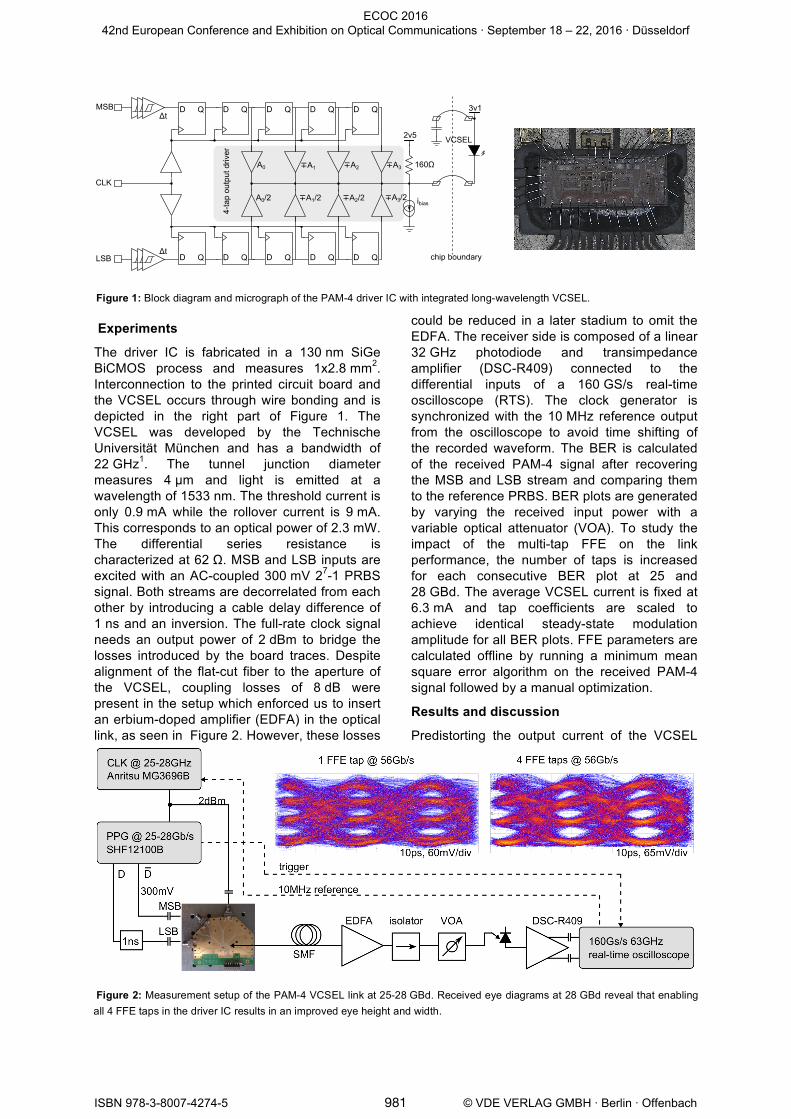
The reported VCSEL driver is an improved and more versatile version of the 40 Gb/s PAM-4 driver5. The block diagram of the data path is shown in Figure 1. Two single-ended binary data streams MSB and LSB are synchronized with each other through retiming flip-flops before they are combined at the output stage. Dimensioning the tap coefficients A0 to A3 in the MSB path twice as large as in the LSB path creates the multi-level current. This current can be predistorted by changing the magnitude and the sign of the coefficients A0 to A3. Each tap can be enabled and configured on demand. This allows us to determine the optimal topology based on power efficiency and bit-error rate (BER) measurements. The delay between consecutive FFE taps is derived from a cascade of flip-flops and corresponds to one symbol period. The effectiveness of the equalization is therefore independent of the data rate. Moreover, this topology consumes less power and area than a fractionally-spaced symbol delay implemented with delay cells6,7. Setup and hold time violations are resolved by preceding the FFE chain with an additional flip-flop and programmable delay cells. The reference clock is converted and amplified to a differential signal to drive the MSB and LSB flip-flops. The back termination resistor is changed from 50 Ω5 to 160 Ω to increase the drive efficiency and dampen the peaking in the optoelectronic response. The driver can deliver a total average current of 29 mA into a 50 Ω equivalent load if the settings for the bias current (ibias) and the FFE coefficients are maximized.
980
ECOC 2016 42nd European Conference and Exhibition on Optical Communications ∙ September 18 – 22, 2016 ∙ Düsseldorf
ISBN 978-3-8007-4274-5 © VDE VERLAG GMBH ∙ Berlin ∙ Offenbach
Experiments
The driver IC is fabricated in a 130 nm SiGe BiCMOS process and measures 1x2.8 mm2. Interconnection to the printed circuit board and the VCSEL occurs through wire bonding and is depicted in the right part of Figure 1. The VCSEL was developed by the Technische Universität München and has a bandwidth of 22 GHz1. The tunnel junction diameter measures 4 µm and light is emitted at a wavelength of 1533 nm. The threshold current is only 0.9 mA while the rollover current is 9 mA. This corresponds to an optical power of 2.3 mW. The differential series resistance is characterized at 62 Ω. MSB and LSB inputs are excited with an AC-coupled 300 mV 27-1 PRBS signal. Both streams are decorrelated from each other by introducing a cable delay difference of 1 ns and an inversion. The full-rate clock signal needs an output power of 2 dBm to bridge the losses introduced by the board traces. Despite alignment of the flat-cut fiber to the aperture of the VCSEL, coupling losses of 8 dB were present in the setup which enforced us to insert an erbium-doped amplifier (EDFA) in the optical link, as seen in Figure 2. However, these losses
could be reduced in a later stadium to omit the EDFA. The receiver side is composed of a linear 32 GHz photodiode and transimpedance amplifier (DSC-R409) connected to the differential inputs of a 160 GS/s real-time oscilloscope (RTS). The clock generator is synchronized with the 10 MHz reference output from the oscilloscope to avoid time shifting of the recorded waveform. The BER is calculated of the received PAM-4 signal after recovering the MSB and LSB stream and comparing them to the reference PRBS. BER plots are generated by varying the received input power with a variable optical attenuator (VOA). To study the impact of the multi-tap FFE on the link performance, the number of taps is increased for each consecutive BER plot at 25 and 28 GBd. The average VCSEL current is fixed at 6.3 mA and tap coefficients are scaled to achieve identical steady-state modulation amplitude for all BER plots. FFE parameters are calculated offline by running a minimum mean square error algorithm on the received PAM-4 signal followed by a manual optimization.
Results and discussion
Predistorting the output current of the VCSEL
Figure 2: Measurement setup of the PAM-4 VCSEL link at 25-28 GBd. Received eye diagrams at 28 GBd reveal that enabling all 4 FFE taps in the driver IC results in an improved eye height and width.
D Q D QD Q D Q D Q
D Q D QD Q D Q D Q
2v5
ibias
160ΩA0
A0/2 ∓A1/2 ∓A2/2 ∓A3/2
∓A1 ∓A2 ∓A3
MSB
CLK
LSB
VCSEL
4-ta
p ou
tput
driv
er
chip boundary
Δt
Δt
3v1
Figure 1: Block diagram and micrograph of the PAM-4 driver IC with integrated long-wavelength VCSEL.
981
ECOC 2016 42nd European Conference and Exhibition on Optical Communications ∙ September 18 – 22, 2016 ∙ Düsseldorf
ISBN 978-3-8007-4274-5 © VDE VERLAG GMBH ∙ Berlin ∙ Offenbach

driver with a 4-tap FFE significantly reduces the inter-symbol interference of the PAM-4 signal as can be noticed in the 28 GBd eye diagrams of Figure 2. This statement can also be derived from the BER plots at 25 and 28 GBd in Figure 3. Considering a RS(544,514) code with a pre-FEC BER limit of 5.2x10⁻⁴, sensitivity is improved by 1.4 dB at 25 GBd and 3.8 dB at 28 GBd. Performance at 0 dBm is well below FEC limit with a BER smaller than 10-6 and error free at 25 GBd. With a record length of 2.8x10⁷
bits, this corresponds to an upper BER limit of 1.7x10⁻⁷ at a 95 % confidence level. At both data rates, the optimization of the 2-tap FFE forces coefficient A1 to zero thereby behaving identical as the 1 tap topology while the transition from 3 to 4 taps leads to a marginal improvement. This small difference is the result of coefficient A2 dominating A3 in a back-to-back link as
summarized in Table 1. Opting for a 3-tap FFE at 56 Gb/s results in 9.6 pJ/bit, which is twice as efficient as recent 56 Gb/s NRZ drivers6,7.
Conclusion
We have developed a BiCMOS PAM-4 driver IC with an integrated 4-tap symbol-spaced FFE that is almost twice as efficient than recent 50 and 56 Gb/s NRZ drivers, favouring PAM-4 over NRZ. Experiments at these data rates with a 22 GHz 1.5 µm VCSEL revealed that the 3-tap configuration is most effective in reducing the BER in a back-to-back link. However, the 4th tap could become crucial when compensating chromatic dispersion in longer SMF links and should be further investigated.
Acknowledgments
The authors would like to thank D. Frederickx and L. Viaene from imec for wire bonding the driver board. This work was supported by the European project MIRAGE (Contr. No.318228).
References
[1] S. Spiga et al., “Single-Mode 1.5-µm VCSELs with 22-
GHz Small-Signal Bandwidth,” Proc. OFC, Paper Tu3D.4, Anaheim, 2016.
[2] F. Karinou et al., “Experimental performance evaluation of equalization techniques for 56 Gb/s PAM-4 VCSEL-based optical interconnects,” Proc. ECOC, pp. 1–3., Valencia, 2015.
[3] R. Rodes et al., “High-Speed 1550 nm VCSEL Data Transmission Link Employing 25 GBd 4-PAM Modulation and Hard Decision Forward Error Correction,” J. Light. Technol., vol. 31, no. 4, pp. 689–695, 2013.
[4] F. Karinou et al., “Directly PAM-4 Modulated 1530-nm VCSEL Enabling 56 Gb/s/λ Data-Center Interconnects,” IEEE Photonics Technol. Lett., vol. 27, no. 17, pp. 1872–1875, Sep. 2015.
[5] W. Soenen et al., “40 Gb/s PAM-4 Transmitter IC for Long-Wavelength VCSEL Links,” IEEE Photonics Technol. Lett., vol. 27, no. 4, pp. 344–347, Feb. 2015.
[6] D. Kuchta et al., “Error-free 56 Gb/s NRZ Modulation of a 1530 nm VCSEL Link,” J. Light. Technol., vol. PP, no. 99, pp. 1–1, 2016.
[7] D. Kuchta et al., "A 50 Gb/s NRZ Modulated 850 nm VCSEL Transmitter Operating Error Free to 90 °C," J. Light. Technol., vol. 33, no. 4, pp. 802-810, 2015
Table 1: Overview of normalized FFE coefficients relative to A0 in a 1-tap configuration and transmitter power dissipation.
25 GBd 28 GBd
A0 A1 A2 A3 P (mW) A0 A1 A2 A3 P (mW)
1,2 taps 1 0 0 0 449 1 0 0 0 469
3 taps 1.11 0 -0.11 0 527 1.11 -0.035 -0.14 0 537
4 taps 1.11 -0.035 -0.07 -0.015 567 1.11 0 -0.14 0.035 560
�7 �6 �5 �4 �3 �2 �1 0
10�1
10�2
10�3
10�4
10�5
10�6
10�7
Average input power (dBm)
BE
R
4 taps3 taps1,2 tapsFEC
�7 �6 �5 �4 �3 �2 �1 0
10�2
10�3
10�4
10�5
10�6
10�7
10�8
Average input power (dBm)
BE
R
4 taps3 taps1,2 tapsFEC
Figure 3: BER plots vs. number of FFE taps at 25 GBd (top) and 28 GBd (bottom).
982
ECOC 2016 42nd European Conference and Exhibition on Optical Communications ∙ September 18 – 22, 2016 ∙ Düsseldorf
ISBN 978-3-8007-4274-5 © VDE VERLAG GMBH ∙ Berlin ∙ Offenbach