


Languages
Pages
Legal

(19) United States (12) Patent Application Publication (10) Pub. No.: US 2012/02484.16 A1
Zhou et al.
US 2012O248416A1
(43) Pub. Date: Oct. 4, 2012
(54)
(75)
(73)
(21)
(22)
(60)
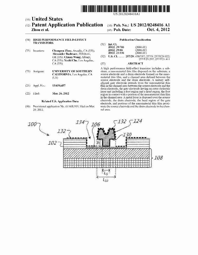
HIGH PERFORMANCE FIELD-EFFECT TRANSISTORS
Inventors: Chongwu Zhou, Arcadia, CA (US); Alexander Badmaev, Hillsboro, OR (US); Chuan Wang, Albany, CA (US); Yuchi Che, Los Angeles, CA (US)
Assignee: UNIVERSITY OF SOUTHERN CALIFORNLA, Los Angeles, CA (US)
Appl. No.: 13/430,457
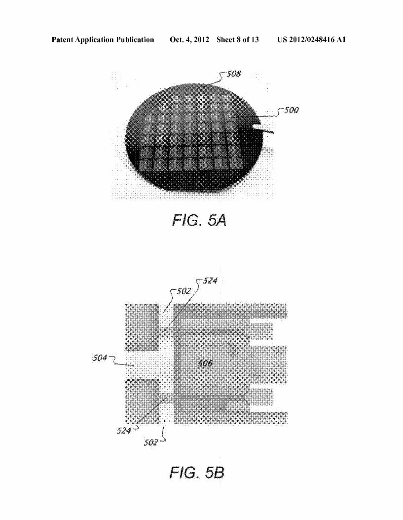
Filed: Mar. 26, 2012
Related U.S. Application Data
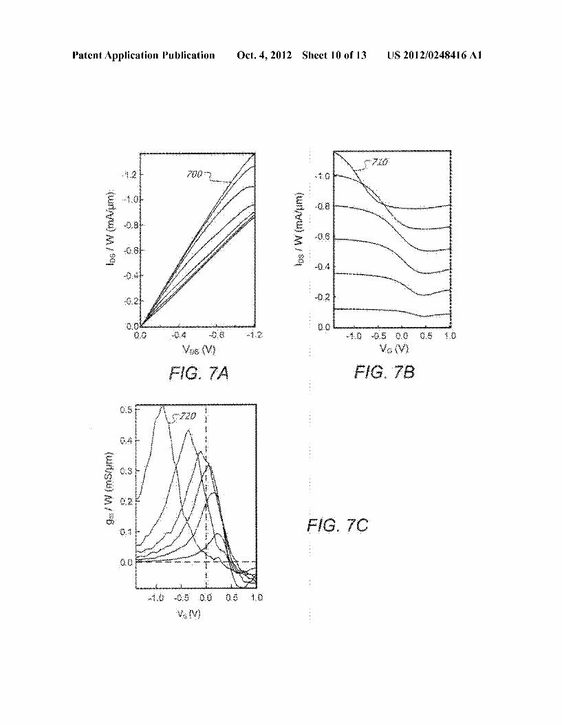
Provisional application No. 61/468,993, filed on Mar. 29, 2011.
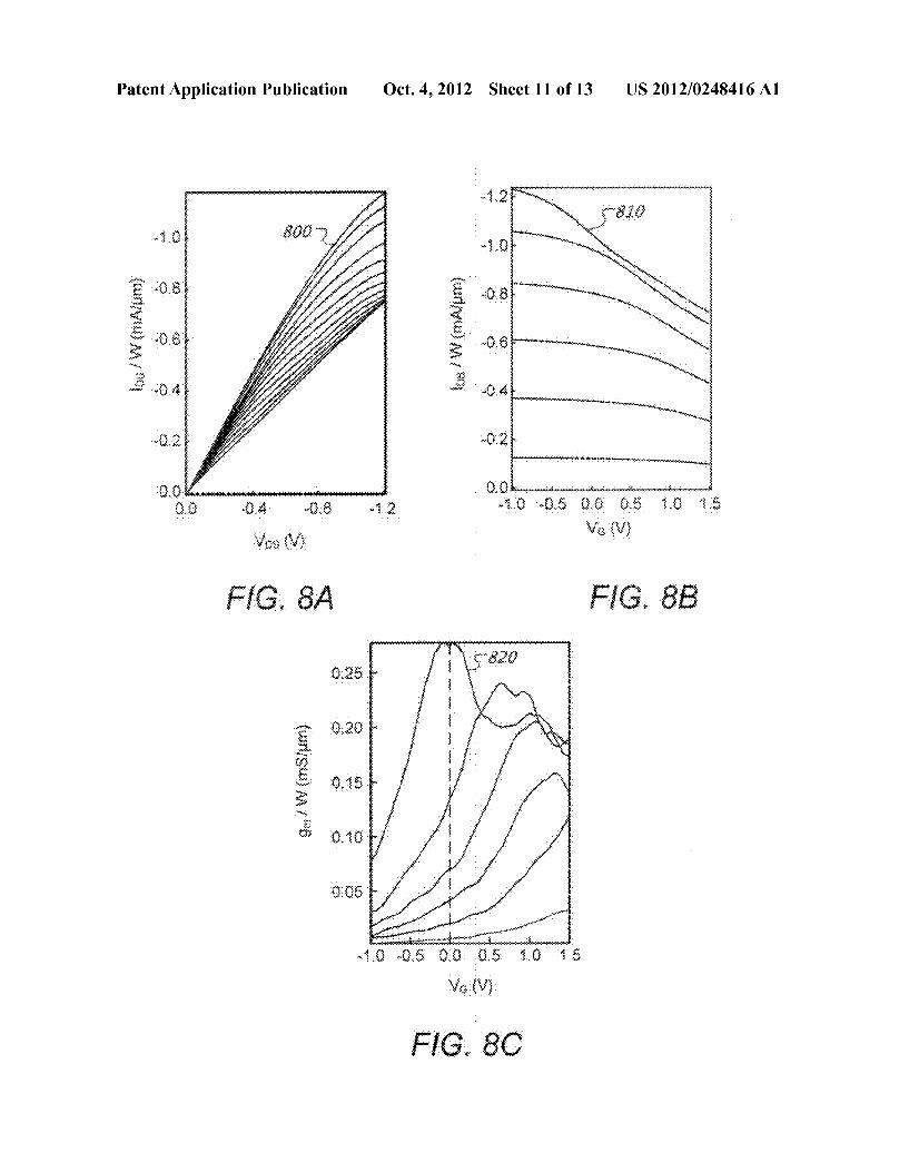
Publication Classification
(51) Int. Cl. HOIL 29/786 (2006.01) HOIL 29/06 (2006.01) HOIL 2/336 (2006.01)
(52) U.S. Cl. ........ 257/29; 438/197; 257/9; 257/E29.022; 257/E29.297; 257/E21.411
(57) ABSTRACT
A high performance field-effect transistor includes a sub strate, a nanomaterial thin film disposed on the Substrate, a Source electrode and a drain electrode formed on the nano material thin film, and a channel area defined between the source electrode and the drain electrode. A unitary self aligned gate electrode extends from the nanomaterial thin film in the channel area between the source electrode and the drain electrode, the gate electrode having an outer dielectric layer and including a foot region and a head region, the foot region in contact with a portion of the nanomaterial thin film in the channel area. A metal layer is disposed over the Source electrode, the drain electrode, the head region of the gate electrode, and portions of the nanomaterial thin film proxi mate the source electrode and the drain electrode in the chan nel area.
E::::::::::::: 8:::::::::::::::::
88:

Patent Application Publication Oct. 4, 2012 Sheet 1 of 13 US 2012/024841.6 A1
106 high - 4 c is i : MMX - - -
s:
S 104
8.
8. :
FIG. 1B
Patent Application Publication Oct. 4, 2012 Sheet 2 of 13 US 2012/024841.6 A1
iii. ::::::::: iii. :::::::::::::::::::::::::::
fg: . . . ... y y t
iii. . :::::::::::::::::::::::::::

Patent Application Publication Oct. 4, 2012 Sheet 3 of 13 US 2012/024841.6 A1
Patent Application Publication Oct. 4, 2012 Sheet 4 of 13 US 2012/024841.6 A1
so so too so go too loo . .
wave eigti in
Patent Application Publication Oct. 4, 2012 Sheet 5 of 13 US 2012/024841.6 A1
FIG. 2B
Patent Application Publication Oct. 4, 2012 Sheet 6 of 13 US 2012/024841.6 A1
Patent Application Publication Oct. 4, 2012 Sheet 7 of 13 US 2012/024841.6 A1
FIG. 4A
S&S&SSS:
420.
FIG. 4C
-----------------------
3.23 3888 3.333 24.30 88:
Patent Application Publication Oct. 4, 2012 Sheet 8 of 13 US 2012/024841.6 A1
FIG. 5A
3.
so

Patent Application Publication Oct. 4, 2012 Sheet 9 of 13 US 2012/024841.6 A1
US 2012/024841.6 A1 Oct. 4, 2012 Sheet 10 of 13 Patent Application Publication
: & ves
FIG 73 was .
FG. 7A
F.G. 7C
kis.
Patent Application Publication Oct. 4, 2012 Sheet 11 of 13 US 2012/024841.6 A1
88: s:
s.
vs. v.
FIG. 8B
o is f / i
7. f
o / ? / Y /
8.
/ /
/ / / / / / / 11
^
M
X -* - M
ww. a- a
sm is xis {w}
FIG. 8C

Patent Application Publication Oct. 4, 2012 Sheet 12 of 13 US 2012/024841.6 A1
i
F.G. 1 O **8388xy 3-ix:
frC. 9

Patent Application Publication Oct. 4, 2012 Sheet 13 of 13 US 2012/024841.6 A1
* 3:38 is: r
root . l ...k.&M ispose atonatesia this iiii or a sixstate
*38 sex.38icia exc3dies - if: ; :8:383 it is
: Apply resist, expose to radiation to form opening, -1206
ii.
Lift of resist, eaving gate electrode between - iii. $83.8fi &is 8
eiectories, with the gate eiectrode asking a rix portion of the aircrateria this in rear the foot of the gate electrode
FIG. 12

US 2012/024841.6 A1
HIGH PERFORMANCE FIELD-EFFECT TRANSISTORS
CROSS-REFERENCE TO RELATED APPLICATION
0001. This application claims priority to U.S. Application Ser. No. 61/468,993, filed on Mar. 29, 2011, and entitled “Design and scalable fabrication approach for high perfor mance field-effect transistors based on carbon nanomateri als, which is incorporated by reference herein in its entirety.
FEDERALLY SPONSORED RESEARCHOR DEVELOPMENT
0002 This invention was made with government support under Grant No. 53-4502-6301 awarded by the National Sci ence Foundation. The government has certain rights in the invention.
FIELD OF THE INVENTION
0003. This invention is related to scalable high perfor mance field-effect transistors.
BACKGROUND
0004 Nanomaterials, such as graphene and carbon nano tubes (CNTs), hold great potential as materials for electronic components, due to remarkable properties such as extremely high charge carrier mobilities and current densities. Single atomic layer thickness provides ultimate electrostatic geom etry for scaling down field-effect transistors (FETs). FETs fabricated with graphene and CNTs have shown improved performance compared to conventional semiconductor devices of the same size, but the performance of FETs fabri cated with these carbon nanomaterials is far from their theo retical potential.
SUMMARY
0005. In a first aspect, fabricating a high performance self aligned field-effect transistor (FET) with a T-shaped gate electrode includes forming a source electrode and a drain electrode on a nanomaterial thin film, thereby defining a channel area between the source electrode and the drain elec trode. The nanomaterial thin film is disposed on a Substrate, and at least a portion of the nanomaterial thin film located outside the channel area is removed from the substrate. A resist is disposed over the source electrode, the drain elec trode, and the nanomaterial thin film in the channel area, and a portion of the resist between the source electrode and the drain electrode is removed, thereby forming an opening in the resist between the source electrode and the drain electrode. The resist is developed, and an electrically conductive mate rial is applied over the developed resist, thereby forming a gate electrode in the opening. The gate electrode includes a head region and a foot region. The foot region is in contact with a portion of the nanomaterial thin film in the channel area and has a length parallel to the Surface of the nanomaterial thin film shorter than the maximum length of the head region parallel to the surface of the nanomaterial thin film. The developed resist is removed, and a dielectric layer is formed on the outer Surface of the gate electrode. A metal layer is deposited over the source electrode, the drain electrode, the head region of the gate electrode, and a second portion of the nanomaterial thin film in the channel area. The head region of
Oct. 4, 2012
the gate electrode inhibits deposition of the metal layer over a third portion of the nanomaterial thin film proximate the foot region of the gate electrode (e.g., when the metal is deposited in a direction normal to the Surface of the nanomaterial thin film.) 0006 Implementations may include one or more of the following features. For example, the opening in the resist is a T-shaped opening, and forming the gate electrode includes forming a T-shaped gate electrode. Forming the Source elec trode and the drain electrode on the nanomaterial thin film includes depositing metal pads on the nanomaterial thin film. Removing at least the portion of the nanomaterial thin film located outside of the channel area includes etching the Sub strate. In some cases, disposing resist over the source elec trode, the drain electrode, and the nanomaterial thin film in the channel area includes forming a bilayer resist mask or a trilayer resist mask. Removing the portion of the resist between the source electrode and the drain electrode includes exposing the portion of the resist to radiation. For example, exposing the portion of the resist to radiation includes expos ing at least some of the portion of the resist to a first dose of radiation, and exposing the rest of the portion to a second dose of radiation, wherein the first dose of radiation is more ener getic than the second dose of radiation. 0007. In some cases, applying the electrically conductive material over the developed resist includes forming a unitary gate electrode in the opening. In certain cases, forming the dielectric layer on the outer surface of the gate electrode includes allowing the gate electrode to oxidize in air, and may include forming a dielectric layer between the foot region of the gate electrode and the portion of the nanomaterial thin film in contact with the foot region. Depositing the metal layer typically includes depositing the metal layer from a direction normal to the surface of the nanomaterial thin film. However, the metal layer may also be deposited from another angle. As described herein, depositing the metal layer over the source electrode, the drain electrode, the head region of the gate electrode, and a second portion of the nanomaterial thin film in the channel area includes self-aligning the Source electrode and the drain electrode (e.g., the T-gate electrode is self-aligned). Fabricating a high performance self-aligned FET with a T-shaped gate electrode may also include dispos ing the nanomaterial thin film on the Substrate before forming the Source electrode and the drain electrode on the nanoma terial thin film.
0008. Some implementations include a FET formed by the first aspect and/or a device including the FET formed by the first aspect. 0009. In a second aspect, a FET includes a substrate, a nanomaterial thin film disposed on the Substrate, a source electrode and a drain electrode formed on the nanomaterial thin film, and a channel area defined between the source electrode and the drain electrode. A gate electrode extends from the nanomaterial thin film in the channel area between the source electrode and the drain electrode, the gate elec trode having an outer dielectric layer and comprising a foot region and a head region, the foot region in contact with a portion of the nanomaterial thin film in the channel area and having a length parallel to the Surface of the nanomaterial thin film shorter than the maximum length of the head region parallel to the surface of the nanomaterial thin film. A metal layer is disposed over the source electrode, the drain elec trode, the head region of the gate electrode, and portions of the nanomaterial thin film proximate the source electrode and
US 2012/024841.6 A1
the drain electrode in the channel area, wherein the portions of the nanomaterial thin film proximate the source electrode and the drain electrode in the channel area are defined by the projection of the head region of the gate electrode onto the nanomaterial thin film in the channel area (e.g., from a direc tion normal to Surface of the nanomaterial thin film). 0010 Implementations may include one or more of the following features. For example, the nanomaterial thin film may include conducting nanomaterials, semiconducting nanomaterials, or a combination thereof. Such as nanomate rials selected from the group consisting of carbon nanotubes, graphene, graphene nanoribbons, and nanowires (e.g., con ducting or semiconducting nanowires). The gate electrode is typically a unitary structure and/or T-shaped. In some cases, the channel length of the FET is at least 100 nm, 200 nm or less, or between 100 nm and 200 nm. In certain cases, the gate electrode includes aluminum, and the outer dielectric layer includes an oxide of aluminum. The gate electrode is typi cally self-aligned. In some cases, a current-gain cut-off fre quency (f) of the field-effect transistoris in a range between 5 GHZ, and 25 GHz. Some implementations include a device including the FET of the second aspect. 0011 Self-aligned FETs with T-shaped gate electrodes described herein provide advantages such as elimination of misalignment, reduction of access resistance by minimizing ungated graphene, and reduced gate charging resistance. The use of large-area nanomaterial thin film preparation, wafer scale transfer, and e-beam lithography to deposit T-shaped gate electrodes allows high-yield, Scalable fabrication. 0012. These general and specific aspects may be imple mented using a device, system or method, or any combination of devices, systems, or methods. The details of one or more embodiments are set forth in the accompanying drawings and the description below. Other features, objects, and advantages will be apparent from the description and drawings, and from the claims.
BRIEF DESCRIPTION OF THE DRAWINGS
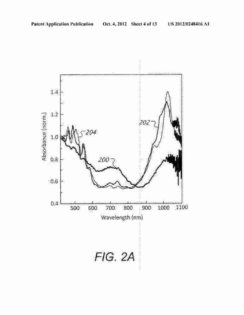
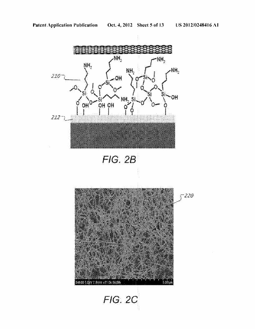
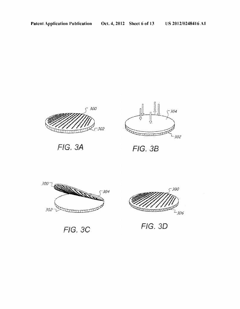
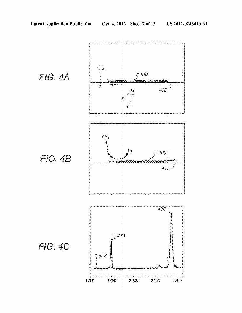
0013 FIGS. 1A-1F depict fabrication of a self-aligned field-effect transistor (FET) with a T-shaped gate electrode. As used herein, “self-aligned FET generally refers to a FET having a self-aligned gate electrode that serves as a mask during fabrication of the FET. FIG. 1G is a perspective view of a self-aligned FET with a T-shaped gate electrode. FIG.1H is a scanning electron microscope (SEM) image of a self aligned FET with a T-shaped gate electrode. 0014 FIG. 2A shows ultraviolet visible—and near infrared absorption spectra of mixed, 95% semiconducting, and 98% semiconducting nanotube solutions. FIG. 2B depicts aminopropyltriethoxysilane assisted separated nano tube deposition on Si/SiO, substrate. FIG. 2C is an SEM image of a thin film network of separated nanotubes using Solution based techniques. 0015 FIGS. 3A-3D depict the synthesis of nanotube arrays on a first substrate and transfer of the synthesized arrays to a second Substrate. 0016 FIG. 4A depicts formation of graphene by chemical vapor deposition (CVD) on nickel. FIG. 4B depicts formation of graphene by CVD on copper. FIG. 4C shows a Raman spectrum of a graphene film grown by CVD on copper and transferred to a Si/SiO substrate.
Oct. 4, 2012
0017 FIG. 5A is a photograph of a 2 inch silicon wafer with fabricated self-aligned graphene FETs having T-shaped gate electrodes. FIG. 5B is an SEM image of a self-aligned graphene FET having a dual gate configuration. 0018 FIG. 6A is a plot showing conductance of a self aligned graphene FET with a T-shaped gate electrode as a function of top gate and back gate Voltages. FIG. 6B shows gate leakage current of self-aligned graphene FETs with T-shaped gate electrodes. FIG. 6C shows scaled resistance Versus top gate Voltage of a self-aligned graphene FET with a T-shaped gate electrode. (0019 FIGS. 7A-7C show DC output and transfer charac teristics of a self-aligned graphene FET with a T-shaped gate electrode and having a channel length of 170 nm. FIG. 7A shows scaled transistor current versus drain voltage. FIG.7B shows scaled transistor current versus gate voltage. FIG. 7C shows scaled transconductance versus gate Voltage. (0020 FIGS. 8A-8C show DC output and transfer charac teristics of a self-aligned graphene FET with a T-shaped gate electrode and having a channel length of 110 nm. FIG. 8A shows scaled transistor current versus drain voltage. FIG. 8B shows scaled transistor current versus gate voltage. FIG. 8C shows scaled transconductance versus gate Voltage. 0021 FIG. 9 shows RF performance of a self-aligned graphene FET with a T-shaped gate electrode and having a channel length of 170 nm. 0022 FIG. 10 shows RF performance of a self-aligned graphene FET with a T-shaped gate electrode and having a channel length of 110 nm. 0023 FIG. 11 shows plots of frequency and intrinsic gate delay versus gate bias for a self-aligned graphene FET with a T-shaped gate electrode and having a channel length of 110
.
0024 FIG. 12 is a flowchart describing a process for fab ricating a self-aligned FET having a T-shaped gate electrode.
DETAILED DESCRIPTION
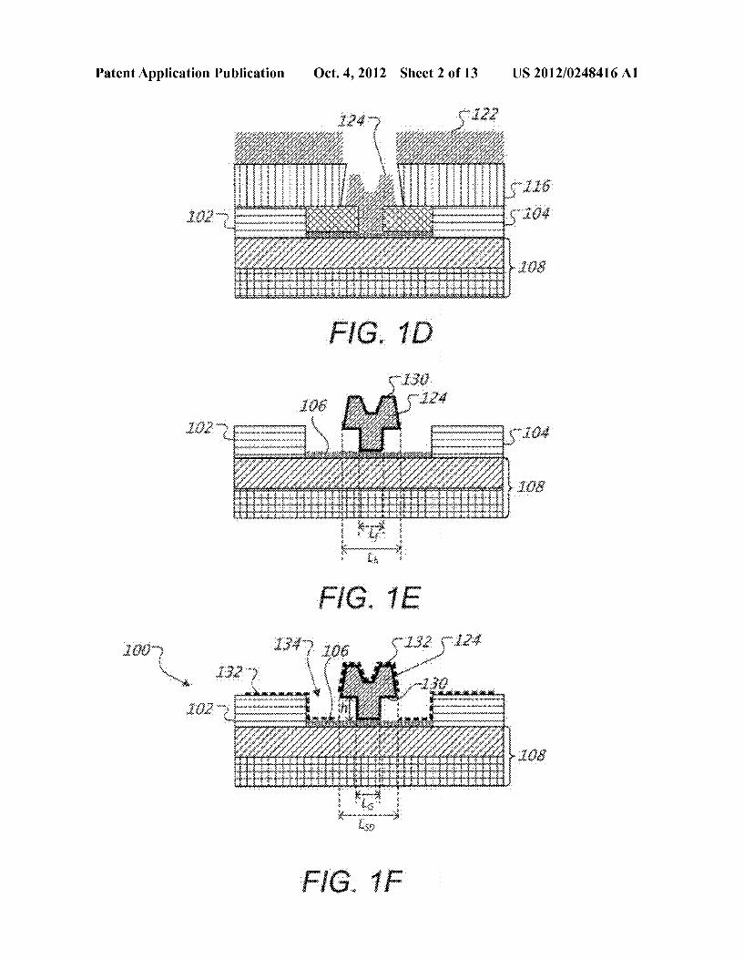
(0025 FIGS. 1A-1E depict fabrication of a high perfor mance field-effect transistor (FET) with a T-shaped gate elec trode (“T-gate electrode' or “T-gate'). FIG.1.A depicts source electrode 102 and drain electrode 104 formed over nanoma terial thin film 106 on substrate 108. In subsequent figures, nanomaterial thin film 106 is understood to be present but not shown between substrate 108 and source and drain electrodes 102 and 104. Substrate 108 is formed by methods generally known in the art and may include one or more layers. As shown in FIG. 1A, substrate 108 includes first layer 110 and second layer 112. First layer 110 is a high resistivity layer formed, for example, from Silicon, quartz, Sapphire, or an insulating material. When first layer 110 is an insulating material, substrate 108 may include first layer 110 in the absence of second layer 112. When present, second layer 112 is an insulator formed, for example, from silicon dioxide or another insulating material. In some instances, second layer 112 is between about 100 nm and about 500 nm thick (e.g., about 300 nm thick). 0026 Nanomaterial thin film 106 may include conducting nanomaterials, semiconducting nanomaterials, or a combina tion thereof. Such as, for example, graphene, graphene nan oribbons, carbon nanotubes (CNTs), nanowires, and the like, or a combination thereof. Nanomaterial thin film 106 is formed by methods including solution-based deposition, array transfer, chemical vapor deposition (CVD), or the like, and then transferred to the surface of substrate 108. Source
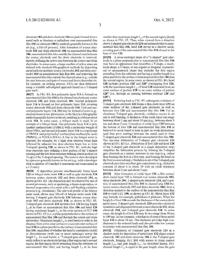
US 2012/024841.6 A1
electrode 102 and drain electrode 104 are pads formed from a metal Such as titanium or palladium over nanomaterial thin film 106 on substrate 108 by methods generally known in the art (e.g., a lift-off process). After formation of source elec trode 102 and drain electrode 104 on nanomaterial thin film 106, nanomaterial thin film outside the channel area between the source electrode and the drain electrode is removed, thereby defining the active area between the source and drain electrodes. In some cases, a large number of active areas are defined with standard lithographical methods by depositing metal pads for multiple source electrodes 102 and drain elec trodes 104 on nanomaterial thin film 106, and removing the nanomaterial thin film outside the channel areas (e.g., outside the area between each pair of Source and drain electrodes) in, for example, an etching process. FETs are then fabricated using a scalable self-aligned approach based on a T-shaped gate Stack. 0027. In FIG. 1B, first polymeric layer 114 is formed on nanomaterial thin film 106 in the channel area between source electrode 102 and drain electrode 104. Second polymeric layer 116 is formed on first polymeric layer 114, covering source electrode 102 and drain electrode 104. First and sec ond polymeric layers 114, 116 may be formed of resist (e.g., electron-beam resist, photoresist, or the like) in a lithographic method generally known in the art, resulting in a bilayer resist mask 118. In some cases, a trilayer mask is used. In an example of a bilayer mask, first polymeric layer 114 is poly (methyl methacrylate) (PMMA) with a molecular weight of about 950k, and second polymeric layer 116 is a copolymer of PMMA and poly(methyl methacrylate-methacrylic acid) (PMMA), or P(MAA-MAA). A line in the bilayer resist is exposed, for example, by a high dose electron beam high followed by adjacent low dose electron beam low to form T-shaped opening 120, as shown in FIG. 1C, with the high dose exposure area defining a foot portion of the T-shaped opening and the low dose exposure defining ahead portion (or T-cap) of the T-shaped opening. The resist is then developed by a process generally known in the art (e.g., with a developer Such as mixture of 4-methyl-2-pentanone and isopropanol in a 1:3 ratio). 0028. A deposition process simultaneously forms layer 122 on bilayer resist mask 118 as well as gate electrode 124 between source electrode 102 and drain electrode 104, as shown in FIG.1D. The deposition may be achieved by one of several processes, such as sputtering, e-beam evaporation, or thermal evaporation of a metal with a self-limiting oxidation process (e.g., aluminum). The side wall profile of the bilayer resist mask allows easy lift-off of bilayer resist mask 118, leaving T-shaped gate electrode 124 between source elec trode 102 and drain electrode 104, as shown in FIG. 1E. T-shaped gate electrode 124 includes foot 126 having length L at its base on nanomaterial thin film 106 and head 128 having maximum length L in the cross section of FET 100 shown in FIG.1E (i.e., a plane perpendicular to the surface of nanomaterial thin film 106 and through the source and drain electrodes). Maximum length L is used herein to refer to the distance from a first outer Surface to a second outer Surface of head 128 in a plane parallel to the surface of nanomaterial thin film 106, regardless of whether the head is continuous (solid) or discontinuous (with one or more openings) across the length L. As used herein, a "T-shaped gate electrode’ gen erally refers to an electrode having a first region and a second region, the first region (foot) extending from the Substrate (or nanomaterial thin film) and having length L, at its base
Oct. 4, 2012
Smaller than maximum length L, of the second region (head) as shown in FIG. 1E. Thus, when viewed from a direction above T-shaped gate electrode 124 and perpendicular to nano material thin film 106, head 128 serves as a shadow mask, covering part of the nanomaterial thin film 106 closest to the base of foot 126. 0029. A cross-sectional shape of a “T-shaped” gate elec trode in a plane perpendicular to nanomaterial thin film 106 may have an appearance that resembles a Y-shape, a mush room shape, a T-shape, or any regular or irregular, symmetri cal or asymmetrical shape that includes the first region extending from the Substrate and having a smaller length in a plane parallel to the surface of nanomaterial thin film 106 than the second region. In some cases, as shown in FIG. 1G, head 128 includes portions 128 and 128" overlapping foot 126, with the maximum length L. of head 128 measured from an outer surface of portion 128 to an outer surface of portion 128" (i.e., through an opening between portions 128 and 128"). 0030 Referring back to FIG. 1E, subsequent oxidation of T-shaped gate electrode 124 forms a thin oxide layer 130 on outer Surfaces of the T-shaped gate electrode, as well as between foot 126 and nanomaterial thin film 106. For an aluminum T-shaped gate electrode, oxidation occurs in air and is self-limiting. A thickness of the oxide layer can range between about 1 nm and about 10 nm (e.g., between about 3 nm and about 5 nm). Formation of oxide layer 130 between the bottom of foot 126 and nanomaterial thin film 106 is believed to occur based at least in part on weak interactions (and thus poor wetting) between the metal used to form T-shaped gate electrode 124 and nanomaterial thin film 106. The one-step fabrication of T-shaped gate electrode 124 shown in FIG. 1D (i.e., fabrication of foot 126 and head 128 of the T-shaped gate electrode in a single deposition step) simplifies the fabrication process by forming the T-shaped gate electrode as a unitary structure in one step (e.g., rather than forming the foot in a first step, and forming the head on the footina second step). Oxidation in air of the T-shaped gate electrode provides excellent gate capacitance (e.g., dielectric constant of about 6 to about 10 with an oxide thickness between about 3 nm and about 5 nm). 0031. After formation of oxide layer 130, a thin source/ drain metal layer 132 is formed over source electrode 102, drain electrode 104, T-shaped gate electrode 124, and a por tion of nanomaterial thin film 106 in channel area 134 (be tween source electrode 102 and drain electrode 104) from a direction normal to the surface of the nanomaterial thin film 106 to yield FET 100, as shown in FIG. 1F. Metal layer 132 may include, for example, palladium or platinum. When the heighth of foot 126 exceeds the thickness of the source/drain metal layer, T-shaped gate electrode 124 provides electrical insulation and alignment between Source electrode 102, drain electrode 104, and T-shaped gate electrode 124. In some cases, the heighth of foot 126 may be in a range from 50 nm to 100 nm. In one example, a thickness of source/drain metal layer 132 is about 10 nm. This thickness provides high con ductance to the external leads and also provides low contact resistance with nanomaterial thin film 106.
0032 Utilization of T-shaped gate electrode 124 as a shadow mask for deposition of metal layer 132 aligns source electrode 102 and drain electrode 104 to the T-shaped gate electrode, forming FET 100 with source to drain contact length Ls and gate length L. As described herein, FET channel length L is equal to the gate length, since the gate
US 2012/024841.6 A1
dielectric thickness is much thinner than the gate length. In Some cases, channel length L is in a range from 100 nm to 200 nm. A length L, of foot 126 can be selected (e.g., by selection of exposure time to the high dose electron beam referred to with respect to FIG.1B) to define the FET channel length, and a length L, of head 128 can be selected (e.g., by selection of exposure time to the low dose electron beam referred to with respect to FIG. 1B) to define the source-drain spacing. The alignment of Source, drain, and gate electrodes and the selection of channel length and source-drain spacing allow for implementation of dimensions selected to reduce parasitic capacitance. Parasitic resistance can be reduced by increasing the height of the T-shaped electrode. The maxi mum height of the T-shaped electrode may range, for example, from 120 nm to 200 nm (e.g., 150 nm). 0033 FIG. 1G is a perspective view of self-aligned FET 100 with a T-shaped gate electrode 124, showing source elec trode 102, drain electrode 104, nanomaterial thin film 106, and substrate 108 having first layer 110 and second layer 112. Source electrode 102 and drain electrode 104 are self-aligned, with nanomaterial thin film 106 visible between metal layer 132 and T-shaped gate electrode 124. FIG. 1H is an SEM image of a portion of a self-aligned FET obtained after cleav ing the Substrate across the transistor channel, showing T-shaped gate electrode 124, metal layer 132, and nanomate rial thin film 106. Although the metal source electrode and drain electrode are not shown, these electrodes are precisely aligned with T-shaped gate electrode 124, and well separated with short sections of ungated nanomaterial thin film 106, forming an air gap or separation distanced (shown in FIG. 1H), corresponding to the length of ungated nanomaterial sections, which leads to a reduction of the parasitic fringe capacitance. 0034. The separation distance d is controlled by the maxi mum length L, of the T-gate head or cap 128 relative to the length Lofthe T-gate foot or base 126, which can be adjusted by the bilayer exposure recipe. Maximum length L, of the T-gate head or cap 128 may be in a range of 50 nm to 250 nm (e.g., 75 nm to 250 nm, 100 nm to 200 nm, or 110 nm to 170 nm), and the length of the ungated nanomaterial sections d may be in a range between about 10 nm and 50 nm (e.g., 20 nm to 40 nm). Although a very wide head or T-cap can be used to reduce gate charging resistance (e.g., with a trilayer resist), here a relatively narrow head or T-cap is used, as a wide T-cap can lead to large area of ungated nanomaterial thin film and thus high access resistance between the self-aligned source? drain and gated nanomaterial thin film. For T-shaped gated electrodes with geometries described herein, use of a bilayer resist mask provides desirable results and is simpler to pro cess than a trilayer recipe. 0035 FETs as described herein allow simultaneous reduc tion of the access resistance, fringe gate-source, gate-drain capacitance, and gate resistance. The length d of the ungated sections can be further reduced by angle deposition of the source/drain metal film, which may lead to a trade-off between further reduction of the access resistance and increase of the parasitic fringe capacitance. Based on calcu lations using gate dimension and experimental measure ments, the gate charging resistance is estimated to be about 1 G2/um of the gate width for a FET having a channel length L. of 100 nm.
0036 Preparation of nanomaterial thin films. As noted with respect to FIG. 1A, nanomaterial thin films used in the fabrication of FETs described herein can be prepared by a
Oct. 4, 2012
number of processes. The prepared nanomaterial thin films are transferred to a substrate, and active areas are defined with lithographical methods generally known in the art by depos iting metal pads (source and drain electrodes) and removing the nanomaterial thin films outside the channel area between the source and drain electrodes. Preparation of large-area nanomaterial thin films in this manner allows Scalable, regis tration-free fabrication and integration of nanomaterials into FETS.
0037 Solution-based deposition. Semiconducting nano tubes used to form a nanomaterial thin film can be separated from metallic nanotubes with Solution methods (e.g., ultra high speed centrifugation in a density gradient), as described in U.S. Patent Application Publication No. 2011/0101302 and C. Wang et al., “Wafer-Scale Fabrication of Separated Carbon Nanotube Thin-Film Transistors for Display Appli cations.” Nano Letters, vol. 9, pp. 4285-4291, both of which are incorporated by reference herein. Plots 200, 202, and 204 in FIG. 2A show ultraviolet-visible-near infrared absorption spectra of mixed nanotubes, 95% semiconducting nanotubes, and 98% conducting nanotubes, respectively. A semiconduct ing nanotube thin film is deposited on a Substrate through incubation in a separated nanotube solution, followed by rinsing with deionized water. An adhesion layer may be dis posed on the substrate before the substrate is contacted with the nanotube solution to improve the adhesion between nano tubes in the solution and the substrate. Suitable adhesive materials include, for example, aminopropyltriethoxysilane (APTES) and poly-L-lysine solution. FIG. 2B depicts inter action between APTES 210 and silica substrate 212, in which condensation reactions occur between hydroxyl groups on the Substrate Surface and alkoxy groups in the silane. Nano tube density on the substrate can be selected by adjusting the concentration of the nanotube solution. FIG. 2C shows an SEM image of nanotube network 220 formed by deposition of a semiconducting nanotube Solution on a Substrate using this Solution-based approach. 0038 Synthesis and transfer of aligned dense arrays of nanotubes. In this method, described in U.S. Patent Applica tion Publication No. 2010/0133511, U.S. Patent Application Ser. No. 61/117,519, and K. Ryu et al., “CMOS-Analogous Wafer-Scale Nanotube-on-Insulator Approach for Submi crometer Devices and Integrated Circuits. Using Aligned Nanotubes.” Nano Letters, vol. 9, pp. 189-197, all of which are incorporated by reference herein, nanotubes are synthe sized by chemical vapor deposition on top of a Substrate (e.g., Sapphire or quartz). The growth of nanotubes is guided by the crystal lattice of the Substrate, yielding dense arrays of long, highly aligned nanotubes. The nanotube arrays can be trans ferred onto another substrate as shown in FIGS. 3A-3D. In FIG. 3A, nanotubes are shown aligned in arrays 300 on sub strate 302. In FIG.3B, layer 304 (e.g., gold film or PMMA) is deposited over nanotube arrays 300 (not shown). In FIG.3C. metallic layer 304, with attached nanotube arrays 300, is peeled away from substrate 302. In FIG. 3D, nanotube arrays 300 are transferred to a second substrate 306 (e.g., silicon or silicon dioxide) with a high or nearly perfect yield. 0039 Large-area graphene film synthesis by chemical vapor deposition and transfer. In this method, described in U.S. patent application Ser. No. 12/576,234 and Y. Zhang et al., “Comparison of Graphene Growth on Single-Crystalline and Polycrystalline Niby Chemical Vapor Deposition.” Jour nal of Physical Chemistry Letters, vol. 1, pp. 3101-3107, both of which are incorporated by reference herein, graphene films
US 2012/024841.6 A1
having one or more layers are synthesized by catalytic chemi cal vapor deposition of carbohydrates on a transition metal Surface (e.g., nickel or copper). This method is Suitable for large-area graphene synthesis, for example, on a wafer having a diameter of 3 to 4 inches. FIG. 4A illustrates the formation of graphene film 400 on nickel substrate 402. FIG. 4B illus trates the formation of graphene film 400 on copper substrate 412. Graphene films 400 can be released from substrates 402 and 412 by etching the Substrate to release the graphene film, and then transferring the graphene film to a second substrate (e.g., silicon or silicon dioxide). FIG. 4C shows a Raman spectrum of a transferred graphene film, with peaks 420 and 422 corresponding to the G-band (graphitic carbon) and (two phonon) 2D-band, respectively. The transferred graphene films are uniform and continuous, with over 90% of the Sur face area having only a single graphene layer. 0040. Other methods. Other suitable preparation methods for nanomaterial thin films including, for example, epitaxial graphene growth on silicon carbide Substrates, described by C. Dimitrakopoulos et al. in “Wafer-scale epitaxial graphene growth on the Si-face of hexagonal SiC (0001) for high fre quency transistors. Journal of Vacuum Science & Technol ogy B, Vol. 28, pp. 985-992, which is incorporated by refer ence herein, and deposition of graphene films from solution, may also be used in the fabrication of FETs.
EXAMPLE
0041 An exemplary self-aligned graphene FET with T-shaped Al/Al2O gate electrode was fabricated as described with respect to FIGS. 1A-1F. Large area single-layer graphene films were synthesized on copper foils by a low pressure CVD method and subsequently transferred onto highly resistive silicon wafer (p-5 kS2 cm) with 300 nm thick top SiO layer. Titanium/palladium (0.5/50 nm) probing pads were first patterned using contact aligner and lift-off process. After this, bilayer electron beam resist, with the top layer, a copolymer of methyl methacrylate and methacrylic acid P(MMA-MAA), being more sensitive than the bottom layer, polymethyl methacrylate (PMMA) with 950 k molecular weight, was used to fabricate a T-shaped top gate stack. The bilayer resist was exposed with high dose electron beam radiation at the gate position center and low dose electron beam radiation at the adjacent area in the same exposure run. After the deposition of aluminium film (140 nm), a standard lift-off process was used to produce the T-shaped gate stack. The Algate electrodes were then oxidized in air, forming a thin dielectric layer between the graphene and Al gate. Finally, a thin layer of palladium (12 nm) was deposited on top of the T-shaped gate electrode to create aligned source and drain electrodes for the graphene FET. 0042. The above-mentioned fabrication method facili tated highly scalable and reliable fabrication of graphene transistors on complete Si wafers. CVD graphene synthesis on copper foils is readily extendable to very large areas by rolling up the foil. Graphene synthesis on copperfoils as large as 12 inchina 4 inch was achieved in a CVD chamber, and the synthesized graphene was successfully transferred to 12 inch Si wafers. Fabrication of self-aligned FETs with T-shaped gate electrodes was carried out on 2 inch Si wafers due to the limitation of available lithography equipment. FIG. 5A is a photograph showing self-aligned graphene FETs 500 fabri cated on a 2 inch Si wafer 508. FIG. 5B is a top-view SEM image of a self-aligned graphene FET 500 having a dual gate
Oct. 4, 2012
configuration, showing source electrode 502, drain electrode 504, graphene 506, and T-shaped gate electrode 524 of FET 500. The scale bar in FIG. 5B corresponds to 10 um. 0043 Performance of the T-shaped Al/Al2O gate stack was characterized using electrical measurements. Conduc tance of a graphene FET as a function of the top gate Voltage V and the back gate Voltage V was assessed. By compar ing the shift of the charge neutrality point V (defined as the top gate Voltage at the minimum conductance point) with the change of the back gate Voltage V, the ratio of top gate dielectric capacitance to the bottom gate dielectric capaci tance was found to be about 130, as calculated from plot 600 in FIG. 6A. For a 300 nm thick SiO, back gate dielectric, the backgate and top gate capacitances were estimated to be 11.8 nF/cm and 1500 nF/cm, respectively. This capacitance cor responds to a dielectric with effective oxidation thickness (EOT) of 2.3 nm, and hence the thickness of the Al-O dielec tric is estimated to be about 3 to 5 nm. The Al-O dielectric exhibited excellent insulator behavior with nearly 100% yield across all the devices. Plots 610 in FIG. 6B shows the gate leakage current (both source and drain grounded) of several self-aligned graphene FETs with T-shaped gate electrodes, indicating that the dielectric breakdown Voltage is higher than 2.5 V.
0044) This fabrication method provides a simple and reli able method to obtain gate stacks with high-quality dielectric for graphene devices. The mobility L and contact resistance R., of a graphene FET can be extracted by fitting the source drain linear resistance Rs with the formula: RsW-2RW+ L/Iue(n+n)'), where L is the channel length or gate length, W is the channel width, no is the residual carrier density, and n is the carrier density due to top gate modula tion. Plot 620 in FIG. 6C shows the experimental data, and plot 630 shows the fit of scaled resistance versus top gate voltage of a graphene FET with 170 nm channel length, having a hole mobility equal to 1500 cm/Vs, residual carrier concentration no of 5x10' cm, and scaled contact resis tance RW of about 400 S2um. 004.5 FIGS. 7A-7C show the output and transfer charac teristics of a graphene FET with a channel length of 170 nm, and FIGS. 8A-8C show the output and transfer characteristics ofagraphene FET with a channellength of 110 nm. Backgate (Substrate) Voltage was kept constant and equal to 0 V for all plots. For the output characteristics (FIG. 7A), the drain volt age Sweeps from 0 V to -1.2V, with the top gate Voltage step of +0.2V starting from -1.6 V for plot 700. The transistors exhibit large drive current densities up to 1.3 mA/um and ~50% gate modulation, as well as appreciable current satu ration with output conductance as low as 0.2 mS/um. The transfer curves (FIG. 7B) and transconductance curves (FIG. 7C) are obtained with gate voltage swept from -1.5V to 1 V. and the drain voltage varied from -1.1 V to -0.1 V (in -0.2V steps) from the top to bottom curves starting from plots 710 and 720 in FIGS. 7B and 7C, respectively. The saturation in I-V, scurves at intermediate gate Voltages shown in FIG.7A is believed to be a result of the presence of the minimal density point close to the drain under the right combination of gate Voltage and drain Voltage. A peak scaled transconduc tance g/W up to 0.5 mS/um was achieved for the 170 nm device.
0046 FIGS. 8A-8C show similar data for a graphene FET with a 110 nm channel length. For the output characteristics (FIG. 8A), the drain voltage sweeps from 0 V to -1.2V, with the top gate voltage step of +0.2 V starting from -1.6 V for

US 2012/024841.6 A1
plot 800. The transfer curves (FIG. 8B) and transconductance curves (FIG. 8C) are obtained with gate voltage swept from -1.5V to 1 V, and the drain voltage varied from -1.1 V to -0.1 V (in -0.2 V steps) from the top to bottom curves starting from plots 810 and 820 in FIGS. 8B and 8C, respectively. As shown in FIGS. 8A-8C, the on/off current ratio and transcon ductance of the FETs with 110 nm channel length are lower than those of the transistors with 170 nm channel length. For example, the peak transconductance, for 110 nm channel length is measured to be 0.27 mS/um (FIG. 8C). One possible reason is the significant contact resistance in the graphene FETs has more pronounced influence on the performance of short channel transistors than long channel transistors. More over, quasi-ballistic transport and strong interband tunneling in graphene may exert influence on short channel transistors. 0047. The high frequency performance of the graphene FETs was further characterized by standard on-chip S-param eter measurements with a vector network analyzer over the frequency range of 0.05 to 10 GHz. The measurements were first calibrated to the probe tips using an off-chip calibration substrate by a standard short-open-load-through (SOLT) pro cedure. A de-embedding procedure was then used to elimi nate the effect of the co-planar waveguide pads on the RF performance by measuring on-chip open and short test structures. The open test structure consisted of only large photolithography-defined pads outside the active area of the transistors, while the short test structure has additional metal film shorting the gate-source and drain-source pads. The S-parameters after this de-embedding procedure are deter mined by the graphene transistor channel, top gate electrode with gate interconnect, and ~1 um long metal source and drain electrodes outside the channel. The de-embedded results are referred to as the device performance, since it is the performance that is accessible for actual integrated on chip circuits. 0048 Plots 900 and 902 in FIG. 9 show the current gain (H. device and H measured, respectively), and plot 904 shows maximum available gain (MAG) for a self-aligned graphene FET with a channel length of 170 nm. The mea sured and device current gains are the results before and after the de-embedding procedure, respectively. Plots 1000 and 1002 in FIG. 10 show the current gain (H. device and He measured, respectively), and plot 1004 shows maximum available gain (MAG) for a self-aligned graphene FET with a channel length of 110 nm. A current-gain cut-off frequency (f) of 15 GHZ, and maximum oscillation frequency (f) of 8 GHz were obtained for the 170 nm device, and f, of 23 GHz and f of 10 GHz were obtained for the 110 nm device. Other FETs fabricated in a similar manner showed f, in the range of 5 GHz to 25 GHz. 0049. The highest achievable current-gain cut-off fre quency in a FET is limited by the intrinsic gate delay and given by f, g/2C, where C is the total gate capacitance. FIG. 11 shows frequency behavior versus gate bias (V) for the self-aligned graphene FET with a channel length of 110 nm. Plots 1100, 1102, and 1104 show g/2JLC current-gain cut-off frequency (f), and maximum oscillation frequency (f), respectively, versus gate bias, allowing comparison of the intrinsic gate delay frequency which is evaluated from the DC measurements of the transconductance and gate capaci tance, and the device current-gain cut-off frequency and maximum oscillation frequency from the RF measurements. The device’ current-gain cut-off frequency is relatively close
Oct. 4, 2012
to the intrinsic gate delay frequency value, Suggesting that the parasitic effects of the T-shaped gate transistor play a small role and justifies the improved device design. 0050. Owing at least in part to the T-shaped gate design, the FETs described herein exhibit excellent microwave power gain with f up to 10 GHz. It is believed that further improvement of both f, and f of the graphene FETs can be achieved by using the T-gate transistor design with metal graphene junction and transferred graphene quality improved. 0051 FIG. 12 is a flowchart describing process 1200 for fabricating a self-aligned FET having a T-shaped gate elec trode. In 1202, a nanomaterial thin film is disposed on a substrate. The nanomaterial thin film may be prepared by methods generally known in the art, including methods described herein. In 1204, the source and drain electrodes are formed on the nanomaterial thin film, and nanomaterial thin film outside of the active area is removed from the substrate as described, for example, with respect to FIG. 1A. In 1206, a resist coating is formed, exposed to radiation, and developed as described, for example, with respect to FIGS. 1 B-1C. In 1208, an electrically conductive layer is disposed on the remaining resist and on the exposed portion of the nanoma terial thin film, thereby forming a gate electrode as described, for example, with respect to FIG. 1D. In 1210, the resist is lifted off, and in 1212 the gate electrode is allowed to oxidize in air to form a dielectric coating as described, for example, with respect to FIG. 1E. In 1214, a metal layer is deposited on the source, drain, and gate electrodes, with the gate electrode masking a portion of the nanomaterial thin film near the foot of the gate electrode and the drain electrode as described, for example, with respect to FIG. 1F, thereby forming self aligned source and drain electrodes. In some cases, portions of process 1200 may be omitted or performed in an order other than that described in FIG. 12. In certain cases, opera tions may be added to process 1200. 0.052 Advantages of the fabrication process described herein include device dimension Scalability, in which gate length (and channel length, as described herein), determined by the length of the foot of the T-shaped gate electrode, can be scaled down below 20 nm with lithographic methods gener ally known in the art, yet can also be compatible with very large scale device width and integration. Another advantage is that the gate resistance can be readily reduced by increasing the cross-sectional area of the head of T-shaped gate elec trode. This reduction in gate resistance allows for improve ment in the power gain of high frequency (radiofrequency) FETs. Moreover, the described fabrication process offers a practical, cost-effective, and reliable method for large scale fabrication and integration of nanomaterials in FETs. 0053. The fabrication method described herein is reliable, allowing for high-yield fabrication of large number of self aligned FETs with T-shaped gate electrodes, and scalable, suitable for further scaling down of device dimensions. While the FETs described herein are analog RF transistors, such self-aligned T-gate fabrication can be combined with selected nanomaterials (e.g., patterned or assembled graphene nanor ibbons) with a bandgap to produce high performance transis tors with high on/off ratio for digital electronics. In addition, self-aligned FETs with T-shaped gate electrodes having con figurations other than those described with respect to FIGS. 1A-1H and FIG.5B may be fabricated by methods described herein.
US 2012/024841.6 A1
0054 Further modifications and alternative embodiments of various aspects will be apparent to those skilled in the art in view of this description. Accordingly, this description is to be construed as illustrative only. It is to be understood that the forms shown and described hereinare to be taken as examples of embodiments. Elements and materials may be substituted for those illustrated and described herein, parts and processes may be reversed, and certain features may be utilized inde pendently, all as would be apparent to one skilled in the art after having the benefit of this description. Changes may be made in the elements described herein without departing from the spirit and scope as described in the following claims.
What is claimed is: 1. A method comprising: forming a source electrode and a drain electrode on a
nanomaterial thin film, thereby defining a channel area between the source electrode and the drain electrode, wherein the nanomaterial thin film is disposed on a Substrate;
removing at least a portion of the nanomaterial thin film located outside of the channel area from the substrate;
disposing resist over the source electrode, the drain elec trode, and the nanomaterial thin film in the channel area;
removing a portion of the resist between the source elec trode and the drain electrode, thereby forming an open ing in the resist between the source electrode and the drain electrode:
developing the resist; applying an electrically conductive material over the devel
oped resist, thereby forming agate electrode in the open ing, the gate electrode comprising a head region and a foot region, the foot region in contact with a portion of the nanomaterial thin film in the channel area and having a length parallel to the Surface of the nanomaterial thin film shorter than the maximum length of the head region parallel to the surface of the nanomaterial thin film;
removing the developed resist; forming a dielectric layer on the outer Surface of the gate
electrode; and depositing a metal layer over the source electrode, the drain
electrode, the head region of the gate electrode, and a second portion of the nanomaterial thin film in the chan nel area, wherein the head region of the gate electrode inhibits deposition of the metal layer over a third portion of the nanomaterial thin film proximate the foot region of the gate electrode.
2. The method of claim 1, wherein the opening in the resist is a T-shaped opening, and forming the gate electrode com prises forming a T-shaped gate electrode.
3. The method of claim 1, wherein forming the source electrode and the drain electrode on the nanomaterial thin film comprises depositing metal pads on the nanomaterial thin film.
4. The method of claim 1, wherein removing at least the portion of the nanomaterial thin film located outside of the channel area comprises etching the Substrate.
5. The method of claim 1, wherein disposing resist over the Source electrode, the drain electrode, and the nanomaterial thin film in the channel area comprises forming a bilayer resist mask.
Oct. 4, 2012
6. The method of claim 1, wherein removing the portion of the resist between the source electrode and the drain electrode comprises exposing the portion of the resist to radiation.
7. The method of claim 6, wherein exposing the portion of the resist to radiation comprises exposing at least Some of the portion of the resist to a first dose of radiation, and exposing the rest of the portion to a second dose of radiation, wherein the first dose of radiation is more energetic than the second dose of radiation.
8. The method of claim 1, wherein applying the electrically conductive material over the developed resist comprises forming a unitary gate electrode in the opening.
9. The method of claim 1, whereinforming the dielectric layer on the outer Surface of the gate electrode comprises allowing the gate electrode to oxidize in air.
10. The method of claim 1, further comprising forming a dielectric layer between the foot region of the gate electrode and the portion of the nanomaterial thin film in contact with the foot region.
11. The method of claim 1, wherein depositing the metal layer comprises depositing the metal layer from a direction normal to the surface of the nanomaterial thin film.
12. The method of claim 1, wherein depositing the metal layer over the source electrode, the drain electrode, the head region of the gate electrode, and a second portion of the nanomaterial thin film in the channel area comprises self aligning the source electrode and the drain electrode.
13. The method of claim 1, further comprising disposing the nanomaterial thin film on the substrate before forming the Source electrode and the drain electrode on the nanomaterial thin film.
14. A field-effect transistor formed by the method of claim 1.
15. A device comprising the field-effect transistor formed by the method of claim 1.
16. A field-effect transistor comprising: a Substrate; a nanomaterial thin film disposed on the Substrate; a source electrode and a drain electrode formed on the
nanomaterial thin film, a channel area defined between the source electrode and
the drain electrode: a gate electrode extending from the nanomaterial thin film
in the channel area between the source electrode and the drain electrode, the gate electrode having an outer dielectric layer and comprising a foot region and a head region, the foot region in contact with a portion of the nanomaterial thin film in the channel area and having a length parallel to the surface of the nanomaterial thin film shorter than the maximum length of the head region parallel to the surface of the nanomaterial thin film;
a metal layer disposed over the Source electrode, the drain electrode, the head region of the gate electrode, and portions of the nanomaterial thin film proximate the source electrode and the drain electrode in the channel area, wherein the portions of the nanomaterial thin film proximate the source electrode and the drain electrode in the channel area are defined by the projection of the head region of the gate electrode onto the nanomaterial thin film in the channel area.
17. The field-effect transistor of claim 16, wherein the nanomaterial thin film comprises conducting nanomaterials, semiconducting nanomaterials, or a combination thereof.
US 2012/024841.6 A1
18. The field-effect transistor of claim 16, wherein the nanomaterial thin film comprises nanomaterials selected from the group consisting of carbon nanotubes, graphene, graphene nanoribbons, and nanowires.
19. The field-effect transistor of claim 16, wherein the gate electrode is a unitary structure.
20. The field-effect transistor of claim 16, wherein the gate electrode is T-shaped.
21. The field-effect transistor of claim 16, wherein a chan nellength of the field-effect transistor is between 100 and 200
.
Oct. 4, 2012
22. The field-effect transistor of claim 16, wherein the gate electrode comprises aluminum, and the outer dielectric layer comprises an oxide of aluminum.
23. The field-effect transistor of claim 16, gate electrode is self-aligned.
24. The field-effect transistor of claim 16, wherein a cur rent-gain cut-off frequency (f) of the field-effect transistoris in a range between 5 GHZ and 25 GHz.
25. A device comprising the field-effect transistor of claim 16.
Top Related