A GUIDE TO USING FETS - Linear Systems · provides a variety of FETs (Field Effect Transistors) ......
18
Three Decades of Quality Through Innovation Linear Integrated Systems • 4042 Clipper Court • Fremont, CA 94538 • Tel: 510 490-9160 • Fax: 510 353-0261 • Email: [email protected] FETS By Ron Quan A GUIDE TO USING FOR SENSOR APPLICATIONS
Transcript of A GUIDE TO USING FETS - Linear Systems · provides a variety of FETs (Field Effect Transistors) ......

Three Decades of Quality Through Innovation
Linear Integrated Systems • 4042 Clipper Court • Fremont, CA 94538 • Tel: 510 490-9160 • Fax: 510 353-0261 • Email: [email protected]
FETSBy Ron Quan
A GUIDE TO USING
FOR SENSOR APPLICATIONS
PAGE 1 A GUIDE TO USING FETS FOR SENSOR APPLICATIONS
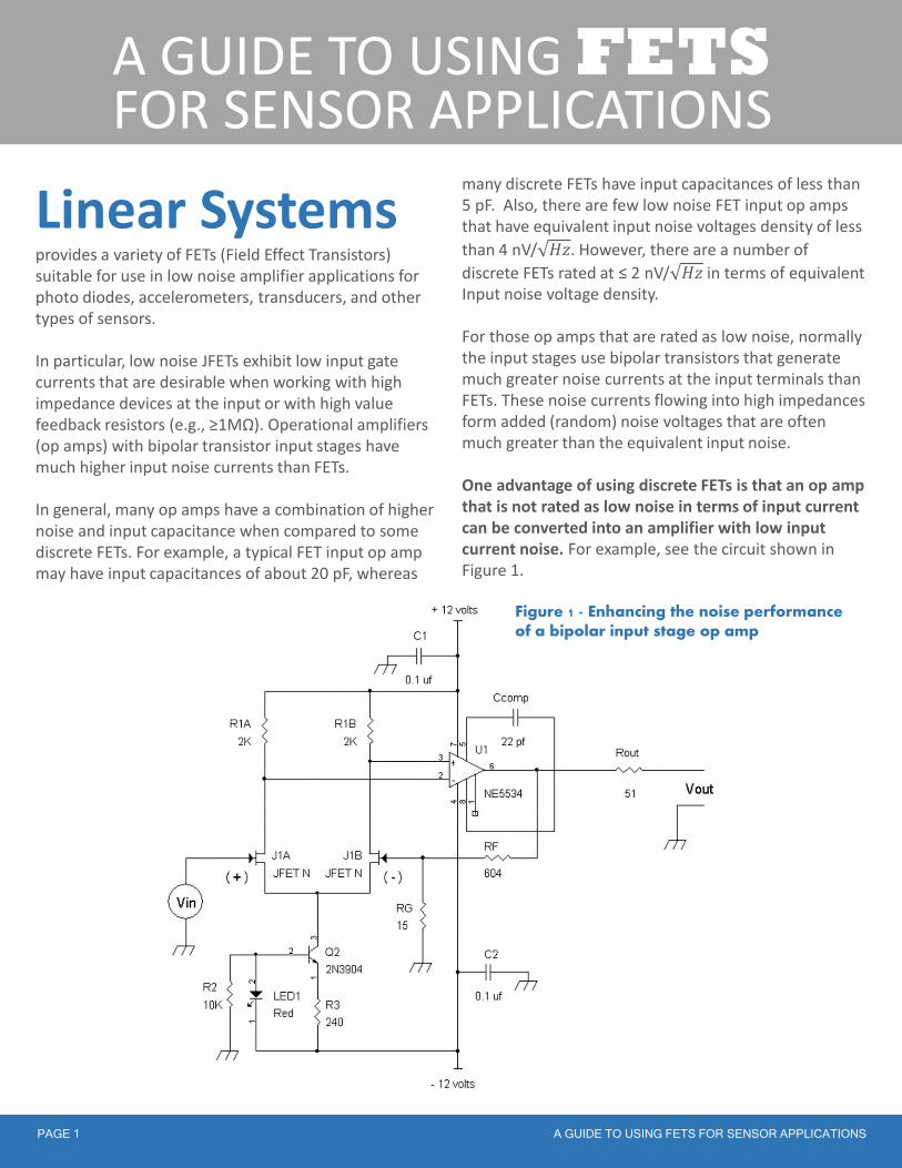
Figure 1 - Enhancing the noise performance of a bipolar input stage op amp
A GUIDE TO USING FETS
Linear Systems provides a variety of FETs (Field Effect Transistors) suitable for use in low noise amplifier applications for photo diodes, accelerometers, transducers, and other types of sensors.
In particular, low noise JFETs exhibit low input gate currents that are desirable when working with high impedance devices at the input or with high value feedback resistors (e.g., ≥1MΩ). Operational amplifiers (op amps) with bipolar transistor input stages have much higher input noise currents than FETs.
In general, many op amps have a combination of higher noise and input capacitance when compared to some discrete FETs. For example, a typical FET input op amp may have input capacitances of about 20 pF, whereas
many discrete FETs have input capacitances of less than 5 pF. Also, there are few low noise FET input op amps that have equivalent input noise voltages density of less
than 4 nV/ 𝐻𝑧. However, there are a number of
discrete FETs rated at ≤ 2 nV/ 𝐻𝑧 in terms of equivalent Input noise voltage density.
For those op amps that are rated as low noise, normally the input stages use bipolar transistors that generate much greater noise currents at the input terminals than FETs. These noise currents flowing into high impedances form added (random) noise voltages that are often much greater than the equivalent input noise.
One advantage of using discrete FETs is that an op amp that is not rated as low noise in terms of input current can be converted into an amplifier with low input current noise. For example, see the circuit shown in Figure 1.
FOR SENSOR APPLICATIONS
In Figure 1 on the previous page, current source Q2, JFETs J1A and J1B with load resistors R1A and R1B form a preamp to the input of U1 to provide better noise performance in terms of input bias current noise and equivalent input noise voltage.
The collector current of Q2 is approximately 1 volt across R3 or about 4 mA. The drain currents of J1A and J1B are equal when Vin = 0, or about 2 mA each. With the load resistors set at 2KΩ, there are about 4 volts DC across each of these resistors. The typical transconductance, gm, for an LSK489 matched dual JFET is about 3 mS = 3 mmho at 2 mA drain current. Thus, the differential mode gain from the gates of J1A and J1B to the drains of J1A and J1B will be approximately 3 mSx 2KΩ = 6.
Note: 1 mho = 1 S = 1 amp/volt, and 1 mmho = 1 mS = 1 ma/volt.
Although an NE5534 op amp has about 4 nV per root Hertz in terms of equivalent noise voltage density, its input bias noise current in the order of 0.60 pA per root Hertz.
The DC gate current of a JFET will typically be less than 0.1 nA, and the input noise current will be:
2𝑞𝐼𝑔 𝐵 = noise current from the gate of the JFET
𝐼𝑔 = gate bias currentq = electron charge = 1.6 x 10⁻¹⁹ coulombB = bandwidth in Hertz. For a noise density calculation, the bandwidth is 1 Hz. Thus, B = 1.
For 0.1 nA = 𝐼𝑔.
2𝑞𝐼𝑔 𝐵 = 0.00566 pA/ 𝐻𝑧 = noise density current
from the gate of the JFET.
In comparison to 0.60 pA/ 𝐻𝑧 for the input noise density current for the NE5534, the JFET has about 100
times lower input noise current at 0.00566 pA/ 𝐻𝑧.
The LSK489 has 1.8 nV/ 𝐻𝑧 of noise voltage density per FET.
For J1A and J1B to be a dual matched JFET transistor such as the LSK489, the equivalent input noise voltage will be about 2.54 nV per root Hertz, or about 3.925 dB
lower noise than the 4 nV/ 𝐻𝑧 rating of the NE5534.
Alternatively, even lower noise can be achieved by using an LSK389B for J1A and J1B, which will result in
an equivalent input noise voltage of 1.27 nV/ 𝑯𝒛. The
LSK389B has typically 0.9 nV/ 𝑯𝒛 per FET.
One should note that the added JFET front circuit (J1A and J1B) will increase the gain bandwidth product of the amplifier by the gain of the FET circuit. For example, at 2 mA per JFET, the tranconductance of the LSK489 is typically 3 mmho or 3 mS. With the 2KΩ load resistors, R1A and R1B, the differential mode gain is about 6. Thus, the 10 MHz gain bandwidth product of the NE5534 is increased to 60 MHz (6 x 10 MHz = 60 MHz). Note the feedback resistors, RF and RG, are set for a gain ≥ 6 to ensure stability in the amplifier without oscillation. That is, (RF/RG) ≥ 5 since the gain is [1 + (RF/RG)].
The tranconductance of the LSK389B is about 3 times more than the LSK489. Thus, if the LSK389 is used in Figure 1, (RF/RG) ≥ 20 to ensure stability without oscillation.
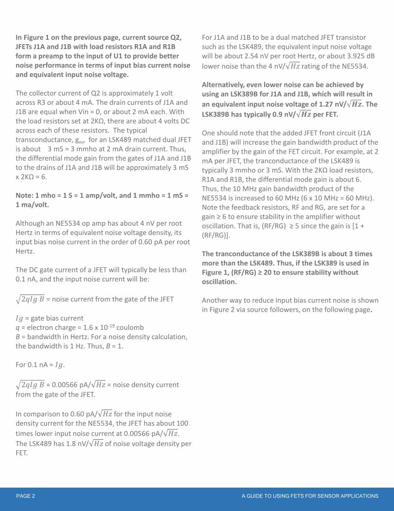
Another way to reduce input bias current noise is shown in Figure 2 via source followers, on the following page.
PAGE 2 GUIDE TO USING JFETSPAGE 2 A GUIDE TO USING FETS FOR SENSOR APPLICATIONS
In Figure 2 above, FETs, J1A and J1B, are configured as source followers to the inputs of an op amp such as a low noise type, AD797 (or LT1028).
In terms of equivalent input voltage noise the AD797
and LT1028 are rated at about 0.9 nV/ 𝐻𝑧. However, their input noise currents are in the order of 1.0
pA/ 𝐻𝑧.
By using the source followers as shown, the input noise
currents are reduced to about 0.00566 pA/ 𝐻𝑧.
For low input capacitance operation (< 3 pF), J1A and J1B can be a matched pair LSK489.
This will result in an equivalent input noise voltage of
2.7 nV/ 𝐻𝑧 with an LSK489. If slightly higher input
capacitance is tolerated (< 5 pF), then an LSK389B is used for an equivalent input noise voltage of 1.55
nV/ 𝐻𝑧.
Q2A and Q2B should be a matched pair of NPN transistors to ensure equal source currents for J1A and J1B. However, often purchasing discrete transistors on tape provides very close DC matching in terms of base to emitter turn on voltage.
Figure 2 - An amplifier with a differential pair source follower to reduce input bias current noise
PAGE 3 A GUIDE TO USING FETS FOR SENSOR APPLICATIONS
One of the common types of sensors today is based on the piezoelectric effect. These types of sensors include accelerometers and hydrophone transducers.
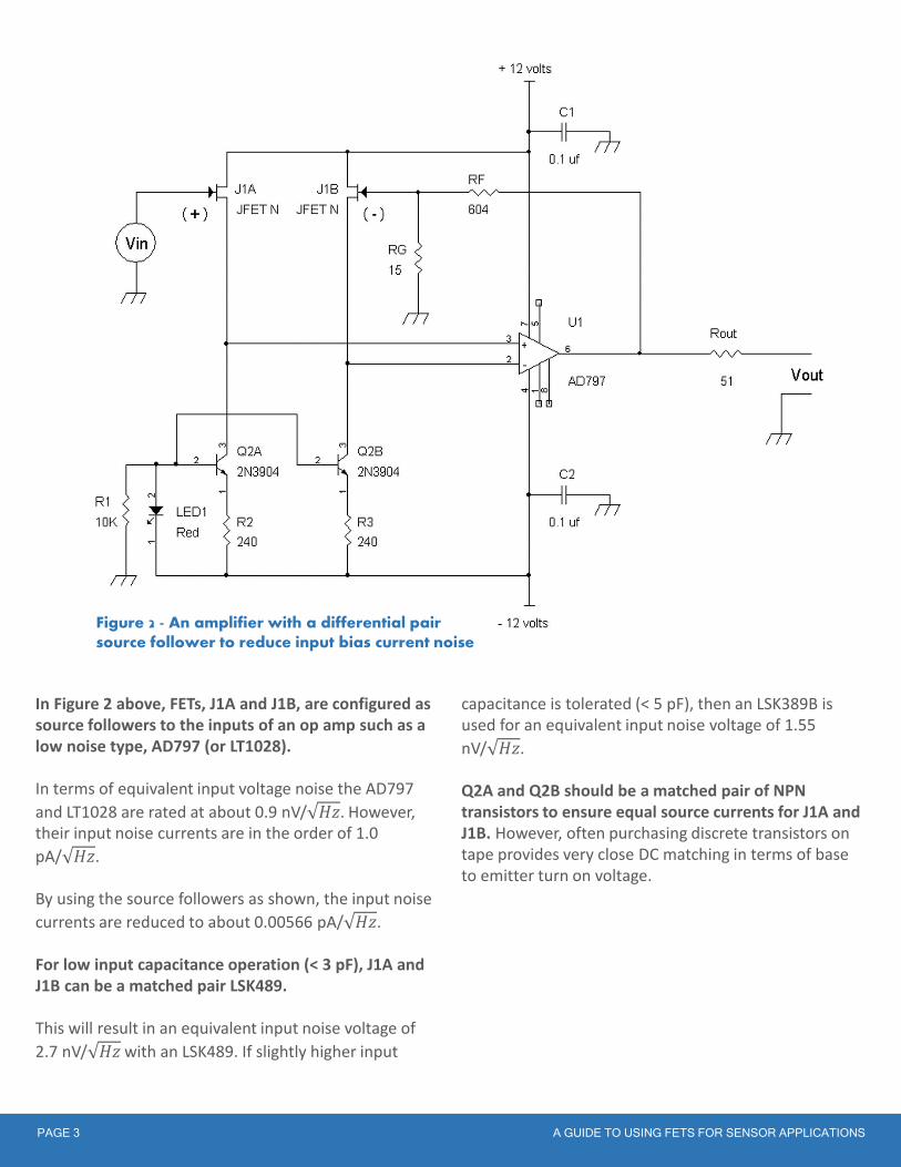
The basic piezoelectric device is modeled at the bottom of the page.
Figure 3(a): Charge model of piezo device.
Figure 3(b): Equivalent voltage model.
In Figure 3(a), a piezoelectric device delivers charge instead of current. The charge, Qpiezo, flows into a capacitor, Cpiezo, to develop a voltage. Recall that:
Qpiezo = Cpiezo x Vpiezo, or expressed another way via algebra:
Vpiezo = Qpiezo/Cpiezo (where Vpiezo is the voltage across the capacitor Cpiezo)
As shown in Figure 3(a), there is also a resistor, Rpiezo, in parallel with the charge generator and capacitor. Rpiezo has a very high resistance, usually very close to an open circuit. For example, the measured DC
resistance across a piezoelectric earphone/microphone is > 2000 MΩ.
However, it may be easier to look at a piezoelectric device as a voltage generator. By equivalently converting the charge source, Qpiezo, and capacitor, Cpiezo into a “Thevenin” voltage source and series impedance, we have the model as shown in Figure 3(b).
From Figure 3(b) we see that the piezoelectric device provides an AC coupled signal and it cannot provide a sustained DC voltage across Rpiezo.
Specific Applications
Piezoelectric Element Preamps
Figure 3(b) - Equivalent voltage model Figure 3(a) - Charge model of piezo device
PAGE 4 A GUIDE TO USING FETS FOR SENSOR APPLICATIONS

From Figure 3(b), we see that the low frequency cut-off response is dependent on the values of Cpiezo and Rpiezo. In practice for the most extended low frequency response, we need Cpiezo to load into a very high resistance value.
For simplicity, let’s take a look at a simple FET buffer amplifier in Figure 4 at the bottom of the page.
Figure 4 A piezo device connected to a simple JFET source follower amplifier.
Generally, R1 can be in the range of 1MΩ to 10MΩ. However, it is not uncommon to have R1 in the order of 100MΩ to 1000MΩ. Source resistor R2 is set to bias the
source to a DC bias current from about 100 μA to 5 mA or R2 can be in the range of 100KΩ to 2KΩ. J1A can be an LSK170 JFET. The drain of J1 is connected to a plus supply voltage and the source provides a signal voltage, Vout with a medium to low impedance output resistance that is able to drive another amplifier. Note that Vout may be connected in series to an AC coupling capacitor to remove the DC voltage at the source of J1A.
Another way to amplify the signal from a piezo device is shown in Figure 5 on the next page. For simplicity, we will ignore the effect of Rpiezo, which is close to infinite resistance.
Figure 4 - A piezo device connected to a simple JFET source follower amplifier
PAGE 5 A GUIDE TO USING FETS FOR SENSOR APPLICATIONS
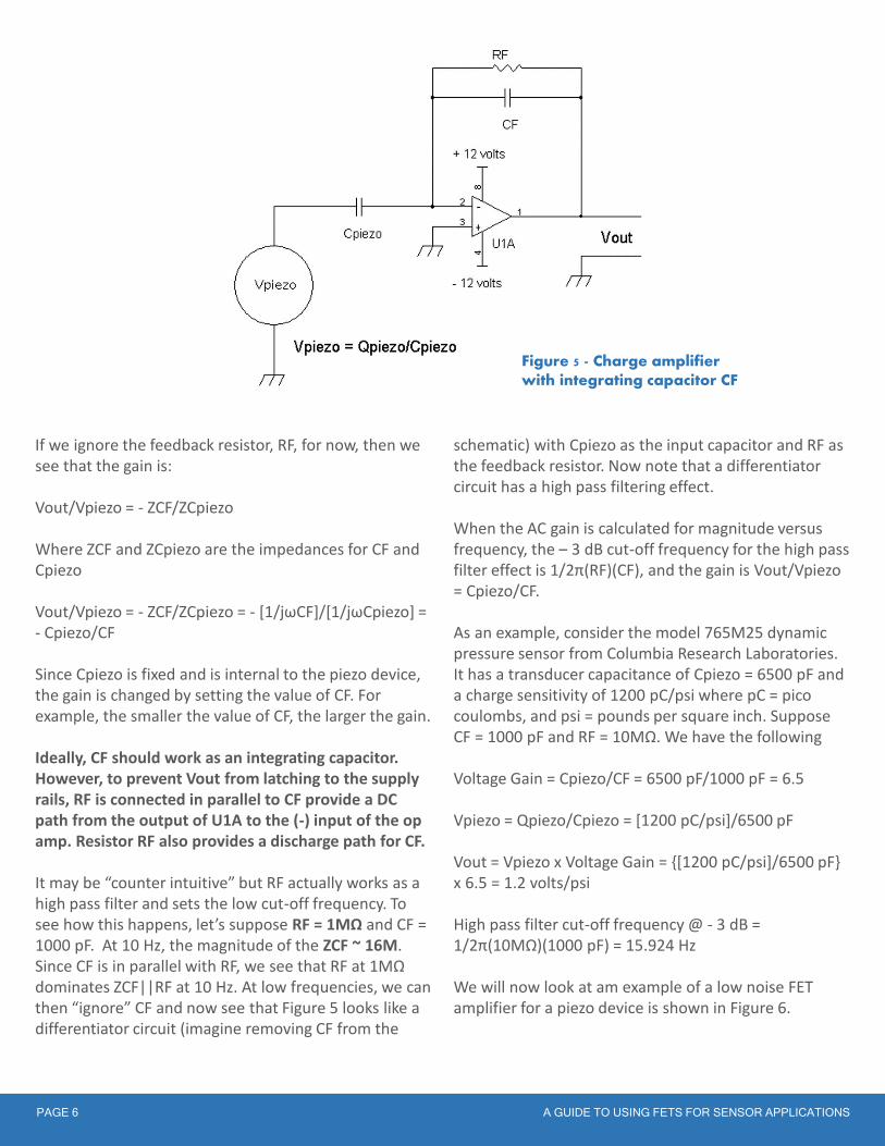
If we ignore the feedback resistor, RF, for now, then we see that the gain is:
Vout/Vpiezo = - ZCF/ZCpiezo
Where ZCF and ZCpiezo are the impedances for CF and Cpiezo
Vout/Vpiezo = - ZCF/ZCpiezo = - [1/jωCF]/[1/jωCpiezo] = - Cpiezo/CF
Since Cpiezo is fixed and is internal to the piezo device, the gain is changed by setting the value of CF. For example, the smaller the value of CF, the larger the gain.
Ideally, CF should work as an integrating capacitor. However, to prevent Vout from latching to the supply rails, RF is connected in parallel to CF provide a DC path from the output of U1A to the (-) input of the op amp. Resistor RF also provides a discharge path for CF.
It may be “counter intuitive” but RF actually works as a high pass filter and sets the low cut-off frequency. To see how this happens, let’s suppose RF = 1MΩ and CF = 1000 pF. At 10 Hz, the magnitude of the ZCF ~ 16M. Since CF is in parallel with RF, we see that RF at 1MΩ dominates ZCF||RF at 10 Hz. At low frequencies, we can then “ignore” CF and now see that Figure 5 looks like a differentiator circuit (imagine removing CF from the
schematic) with Cpiezo as the input capacitor and RF as the feedback resistor. Now note that a differentiator circuit has a high pass filtering effect.
When the AC gain is calculated for magnitude versus frequency, the – 3 dB cut-off frequency for the high pass filter effect is 1/2π(RF)(CF), and the gain is Vout/Vpiezo= Cpiezo/CF.
As an example, consider the model 765M25 dynamic pressure sensor from Columbia Research Laboratories. It has a transducer capacitance of Cpiezo = 6500 pF and a charge sensitivity of 1200 pC/psi where pC = picocoulombs, and psi = pounds per square inch. Suppose CF = 1000 pF and RF = 10MΩ. We have the following
Voltage Gain = Cpiezo/CF = 6500 pF/1000 pF = 6.5
Vpiezo = Qpiezo/Cpiezo = [1200 pC/psi]/6500 pF
Vout = Vpiezo x Voltage Gain = [1200 pC/psi]/6500 pF x 6.5 = 1.2 volts/psi
High pass filter cut-off frequency @ - 3 dB = 1/2π(10MΩ)(1000 pF) = 15.924 Hz
We will now look at am example of a low noise FET amplifier for a piezo device is shown in Figure 6.
Figure 5 - Charge amplifier with integrating capacitor CF
PAGE 6 A GUIDE TO USING FETS FOR SENSOR APPLICATIONS
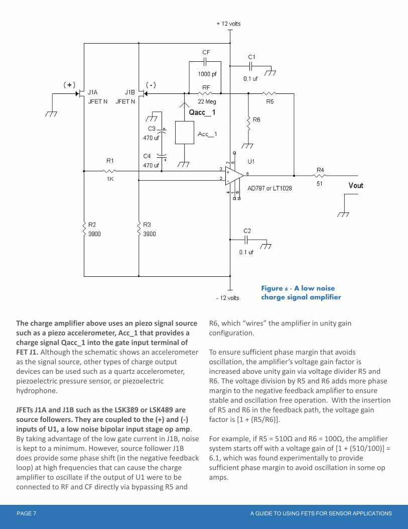
The charge amplifier above uses an piezo signal source such as a piezo accelerometer, Acc_1 that provides a charge signal Qacc_1 into the gate input terminal of FET J1. Although the schematic shows an accelerometer as the signal source, other types of charge output devices can be used such as a quartz accelerometer, piezoelectric pressure sensor, or piezoelectric hydrophone.
JFETs J1A and J1B such as the LSK389 or LSK489 are source followers. They are coupled to the (+) and (-) inputs of U1, a low noise bipolar input stage op amp. By taking advantage of the low gate current in J1B, noise is kept to a minimum. However, source follower J1B does provide some phase shift (in the negative feedback loop) at high frequencies that can cause the charge amplifier to oscillate if the output of U1 were to be connected to RF and CF directly via bypassing R5 and
R6, which “wires” the amplifier in unity gain configuration.
To ensure sufficient phase margin that avoids oscillation, the amplifier’s voltage gain factor is increased above unity gain via voltage divider R5 and R6. The voltage division by R5 and R6 adds more phase margin to the negative feedback amplifier to ensure stable and oscillation free operation. With the insertion of R5 and R6 in the feedback path, the voltage gain factor is [1 + (R5/R6)].
For example, if R5 = 510Ω and R6 = 100Ω, the amplifier system starts off with a voltage gain of [1 + (510/100)] = 6.1, which was found experimentally to provide sufficient phase margin to avoid oscillation in some op amps.
Figure 6 - A low noise charge signal amplifier
PAGE 7 A GUIDE TO USING FETS FOR SENSOR APPLICATIONS
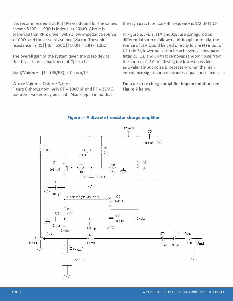
It is recommended that R5||R6 << RF, and for the values chosen 510Ω||100Ω is indeed << 10MΩ. Also it is preferred that RF is driven with a low impedance source < 100Ω, and the drive resistance (via the Theveninresistance) is R5||R6 = 510Ω||100Ω = 83Ω < 100Ω.
The overall gain of the system given the piezo device that has a rated capacitance of Cpiezo is:
Vout/Vpiezo = - [1 + (R5/R6)] x Cpiezo/CF
Where Vpiezo = Qpiezo/CpiezoFigure 6 shows nominally CF = 1000 pF and RF = 22MΩ, but other values may be used. Also keep in mind that
the high pass filter cut-off frequency is 1/2π(RF)(CF)
In Figure 6, JFETs, J1A and J1B, are configured as differential source followers. Although normally, the source of J1A would be tied directly to the (+) input of U1 (pin 3), lower noise can be achieved via low pass filter R1, C3, and C4 that removes random noise from the source of J1A. Achieving the lowest possible equivalent input noise is necessary when the high impedance signal source includes capacitance across it.
For a discrete charge amplifier implementation see Figure 7 below.
Figure 7 - A discrete transistor charge amplifier
PAGE 8 A GUIDE TO USING FETS FOR SENSOR APPLICATIONS
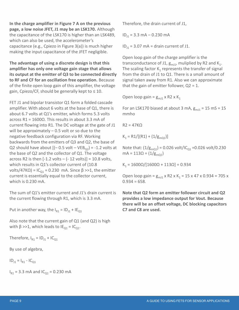
In the charge amplifier in Figure 7 A on the previous page, a low noise JFET, J1 may be an LSK170. Although the capacitance of the LSK170 is higher than an LSK489, which can also be used, the accelerometer’s capacitance (e.g., Cpiezo in Figure 3(a)) is much higher making the input capacitance of the JFET negligible.
The advantage of using a discrete design is that this amplifier has only one voltage gain stage that allows its output at the emitter of Q3 to be connected directly to RF and CF for an oscillation free operation. Because of the finite open loop gain of this amplifier, the voltage gain, Cpiezo/CF, should be generally kept to ≤ 10.
FET J1 and bipolar transistor Q1 form a folded cascade amplifier. With about 6 volts at the base of Q1, there is about 6.7 volts at Q1’s emitter, which forms 5.3 volts across R1 = 1600Ω. This results in about 3.3 mA of current flowing into R1. The DC voltage at the gate of J1 will be approximately – 0.5 volt or so due to the negative feedback configuration via RF. Working backwards from the emitters of Q3 and Q2, the base of Q2 should have about [(– 0.5 volt – VEBQ2) = -1.2 volts at the base of Q2 and the collector of Q1. The voltage across R2 is then [-1.2 volts – (- 12 volts)] = 10.8 volts, which results in Q1’s collector current of (10.8 volts/47KΩ) = ICQ1 = 0.230 mA. Since β >>1, the emitter current is essentially equal to the collector current, which is 0.230 mA.
The sum of Q1’s emitter current and J1’s drain current is the current flowing through R1, which is 3.3 mA.
Put in another way, the IR1 = IDJ1 + IEQ1
Also note that the current gain of Q1 (and Q2) is high with β >>1, which leads to IEQ1 = ICQ1.
Therefore, IR1 = IDJ1 + ICQ1
By use of algebra,
IDJ1 = IR1 - ICQ1
IR1 = 3.3 mA and ICQ1 = 0.230 mA
Therefore, the drain current of J1,
IDJ1 = 3.3 mA – 0.230 mA
IDJ1 = 3.07 mA = drain current of J1.
Open loop gain of the charge amplifier is the transconductance of J1, gmJ1, muliplied by R2 and K1. The scaling factor K1 represents the transfer of signal from the drain of J1 to Q1. There is a small amount of signal taken away from R1. Also we can approximate that the gain of emitter follower, Q2 = 1.
Open loop gain = gmJ1 x R2 x K1
For an LSK170 biased at about 3 mA, gmJ1 = 15 mS = 15 mmho
R2 = 47KΩ
K1 = R1/[(R1) + (1/gmQ1)]
Note that: (1/gmQ1) = 0.026 volt/ICQ1 =0.026 volt/0.230 mA = 113Ω = (1/gmQ1)
K1 = 1600Ω/[1600Ω + 113Ω] = 0.934
Open loop gain = gmJ1 x R2 x K1 = 15 x 47 x 0.934 = 705 x 0.934 = 658.
Note that Q2 form an emitter follower circuit and Q2 provides a low impedance output for Vout. Because there will be an offset voltage, DC blocking capacitors C7 and C8 are used.
PAGE 9 A GUIDE TO USING FETS FOR SENSOR APPLICATIONS
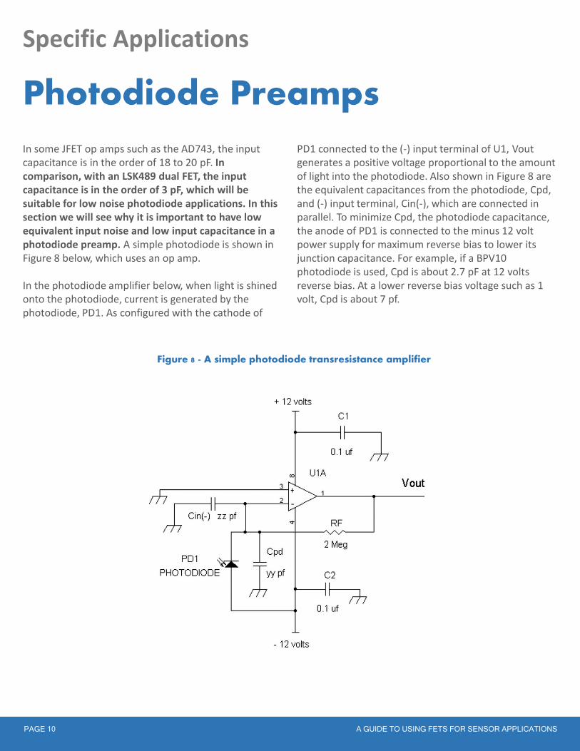
In some JFET op amps such as the AD743, the input capacitance is in the order of 18 to 20 pF. In comparison, with an LSK489 dual FET, the input capacitance is in the order of 3 pF, which will be suitable for low noise photodiode applications. In this section we will see why it is important to have low equivalent input noise and low input capacitance in a photodiode preamp. A simple photodiode is shown in Figure 8 below, which uses an op amp.
In the photodiode amplifier below, when light is shined onto the photodiode, current is generated by the photodiode, PD1. As configured with the cathode of
PD1 connected to the (-) input terminal of U1, Voutgenerates a positive voltage proportional to the amount of light into the photodiode. Also shown in Figure 8 are the equivalent capacitances from the photodiode, Cpd, and (-) input terminal, Cin(-), which are connected in parallel. To minimize Cpd, the photodiode capacitance, the anode of PD1 is connected to the minus 12 volt power supply for maximum reverse bias to lower its junction capacitance. For example, if a BPV10 photodiode is used, Cpd is about 2.7 pF at 12 volts reverse bias. At a lower reverse bias voltage such as 1 volt, Cpd is about 7 pf.
Specific Applications
Photodiode Preamps
Figure 8 - A simple photodiode transresistance amplifier
PAGE 10 A GUIDE TO USING FETS FOR SENSOR APPLICATIONS
For low noise considerations, these two capacitances, Cpd and Cin(-), should be low as possible. The reason is that the equivalent input noise density voltage, Vnoise_input of the op amp will be amplified in the following manner at Vout, neglecting any noise current from the photodiode:
Vout_noise for a bandwidth of 1 Hz = (Vnoise_input)
1 + (𝜔𝑅𝐹𝐶𝑡)2 + 4𝑘𝑇𝑅𝐹 (1)
Where 𝜔 = 2πf, 𝑅𝐹 = feedback resistor, k = 1.38 x10⁻²³
Joules per degrees Kelvin, T = 298 degrees Kelvin
𝐶𝑡 = Cpd||Cin(-) = total capacitance at the (-) input terminal, and𝐶𝑡 = Cpd + Cin(-)
4𝑘𝑇𝑅𝐹 = thermal noise voltage of the feedback resistor RF for a bandwidth of 1 Hz.
As we can see from the equation above, the output noise, Vout_noise, goes higher if Ct is increased.
In designing a low noise transresistance preamps the goals are to:
1. Minimum equivalent input noise voltage. Equation (1) above shows that the output noise voltage is dependent on the equivalent input noise voltage, Vnoise_input.
2. Minimize noise current from the (-) input because the noise current at the input will form a noise voltage across the feedback resistor. Generally, a JFET is desirable for the (-) input because of its low gate noise current.
3. Minimize the capacitance from the (-) input to ground. The equation (1) shows that more noise is generated at the output when the capacitance, Ct = Cpd + Cin(-), at the (-) input terminal is increased.
4. Use as large value RF as possible. At first glance, it would appear increasing the resistance in RF would increase the output noise because of the resistor’s thermal noise. This is true but the signal
amplification from the photodiode is increased more so that results in a net increase in signal to noise ratio when RF is increased in value. For example, doubling the value in RF increases the
resistor noise from RF by 2 = 1.41 while increasing the photodiode signal output voltage by 2. Thus,
there is a net gain of 2 or + 3 dB, in terms of signal to noise ratio in this example.
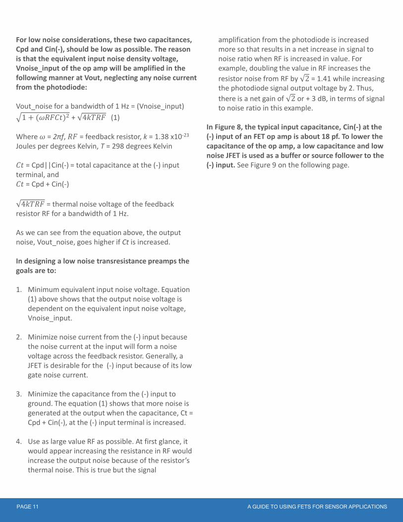
In Figure 8, the typical input capacitance, Cin(-) at the (-) input of an FET op amp is about 18 pf. To lower the capacitance of the op amp, a low capacitance and low noise JFET is used as a buffer or source follower to the (-) input. See Figure 9 on the following page.
PAGE 11 A GUIDE TO USING FETS FOR SENSOR APPLICATIONS
A low noise JFET such as an LSK189 is configured as a source follower, with a source biasing resistor R3. In terms of input capacitance at the gate of J1 with an LSK189, it is about 3 pF from the gate to the drain, which is much less than the 18 pF of Cin(-). Capacitance between the gate and ground due to the gate to source capacitance approaches zero. This is because the source follower configuration provides substantially the same AC voltage at the gate and at the source, which substantially cancels out the capacitance between the gate and the source. The source follower also greatly reduces the capacitance seen at the gate to ground even when the source is driving signal into a capacitive load, Cin(-), the capacitance at the (-) input terminal of the op amp U1A.
It should be noted that the source follower circuit may add some phase shift to the overall amplifier circuit. To ensure phase margin and no oscillations, a resistive divider R1 and R2 is used. With the values given at 3900Ω for R1 and R2, the equivalent feedback resistance is [1 + (R2/R1)] x RF = 2 x 1MΩ = 2MΩ, the same resistance value shown in Figure 8 for RF.If the (+) input of the op amp in Figure 9 is grounded,
such that Voffset = 0 volts, Vout will most likely have a DC offset. To “zero” Vout when there is no signal from the photodiode, a clean DC voltage, Voffset may be applied to the (+) input of U1.
Op amp U1A = AD797 has an equivalent input noise
voltage of 0.9 nV/ 𝐻𝑧 and J1 =LSK189 with an
equivalent input noise voltage of 1.8 nV/ 𝐻𝑧, the total
equivalent input noise voltage is about 2.0 nV/ 𝐻𝑧. This is lower than a very low noise JFET op amp such as an
AD743 that has 3.2 nV/ 𝐻𝑧. Note that bipolar input
stage op amps AD797 with 0.9 nV/ 𝐻𝑧 has lower
equivalent input noise voltage than 2.0 nV/ 𝐻𝑧, but the AD797’s input noise current is too high and are not suitable for amplifier circuits with large value feedback resistors (RF) in the MΩ such as the circuit shown in Figure 8.
Note that J1 may be substituted with an LSK170
(0.9nV/ 𝑯𝒛 ) if a slight increase in capacitance from the gate to ground is acceptable. This FET has about half the equivalent input noise of the LSK189.
Figure 9 - A low capacitance JFET added to an op amp circuit to lower input capacitance and reduce noise
PAGE 12 A GUIDE TO USING FETS FOR SENSOR APPLICATIONS
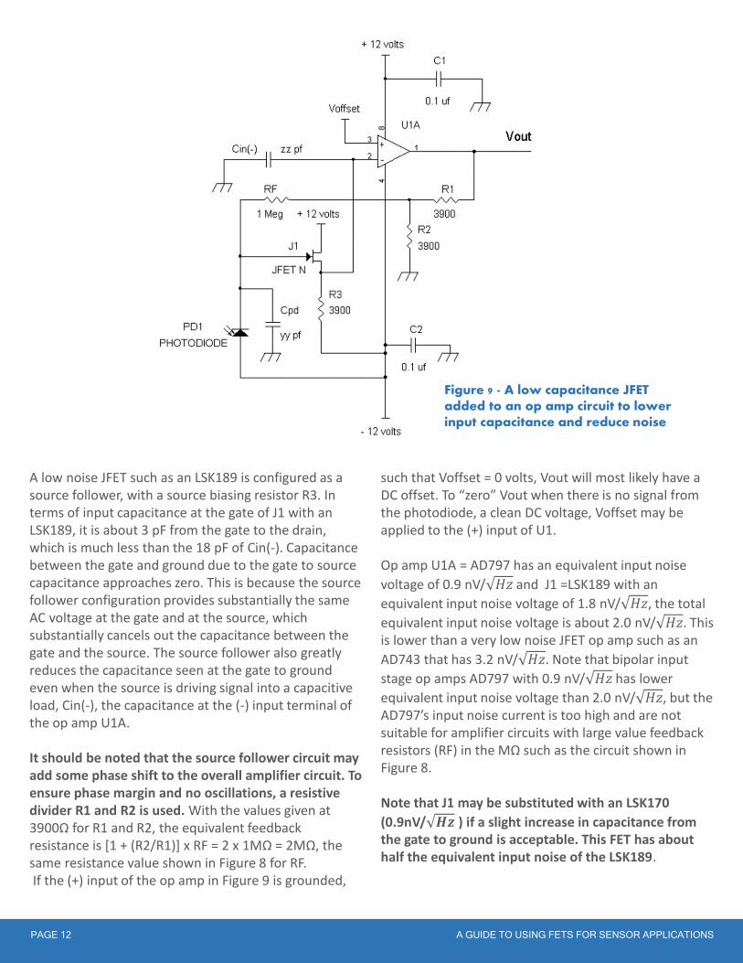
In transresistance amplifiers, a feedback resistor will have a capacitance, CF, across its leads. This capacitance will reduce the bandwidth of the output signal at high frequencies. See Figures 10(a) and 10(b) below.
Figure 10(a) shows a photodiode preamp with Ct = Cpd+ Cin(-), and CF a capacitor across the feedback resistor RF. CF can be the internal parasitic capacitance from resistor RF, or it can be capacitor often connected across RF to add positive phase shift that offsets the negative shift from Ct. This added positive phase shift due to CF ensures stability in the photodiode preamp. However, one side effect from CF is reducing the bandwidth of the
amplified photodiode signal at Vout.
The -3 dB bandwidth at Vout is 1/[2π(RF)(CF)] = f-3dB
For example, RF = 2MΩ and CF = 1pF, then f-3dB = 1/[2π(2MΩ)( 1pF)] = 79.6 kHzOne way to reduce the effects this roll off in frequency response is to make RF a series connection of ten 200KΩ resistors. If CF is still 1pF, the new bandwidth will be: f-3dB = 1/[2π(200KΩ)( 1pF)] = 796 kHz
However, there is another alternative and that is to equalize the frequency response as shown in Figure 10(b).
Specific Applications
Extending the Frequency Response of a TransresistanceAmplifier
PAGE 13 A GUIDE TO USING FETS FOR SENSOR APPLICATIONS
Figure 10(b) - Simple preamp with equalization.Figure 10(a) - Simple preamp.
For now, let’s assume that that op amp U1A in Figure10(b) has sufficient phase margin to not oscillate when RA = 0Ω, and when RB = open circuit or removed.
If (R1 + R2)(C3) = (RF)(CF) there will be a “boost” that compensates for the roll-off. When the boost ends is determined by the (R2)(C2) time constant. The amount of bandwidth extension is [1+ (R1/R2)]. Generally there is a limit on bandwidth extension. If R2 0Ω, then C3 is grounded and forms a low pass filter and lagging phase shift network with R1, that will most likely cause oscillation.
Generally, it is recommended to start with R2 = 33% of R1, which gives a bandwidth extension of [1 + (R1/0.33R1)] = [1 + 3] = 4 = bandwidth extension.
For example, if RF= 2MΩ and CF = 1pF, we want R1
<<RF, so let’s make R1 = 10KΩ and R2 = 3.3KΩ, then (R1 + R2)(C3) = (RF)(CF) or (10KΩ + 3.3KΩ)(C3) = (13.3KΩ)(C3) = (2MΩ)(1pF), or
C3 = (2MΩ)(1pF)/(13.3KΩ) = 150 pf = C3. With these values, the frequency response will increase from 79.6 kHz to about 318 kHz for Figure 10(b).
Note: Often the op amp U1A may require voltage divider resistors RA and RB to ensure sufficient phase margin so that the amplifier in Figure10(b) does not oscillate. Typically, start out with a voltage divider of 2 or more. That is, (RA/RB) ≥ 1. Also, it is recommended that RA||RB ≤ 500Ω and that RA||RB << R1.
Figure 11 shows an equalized preamplifier with discrete FETs at the input terminals.
PAGE 14 A GUIDE TO USING FETS FOR SENSOR APPLICATIONS
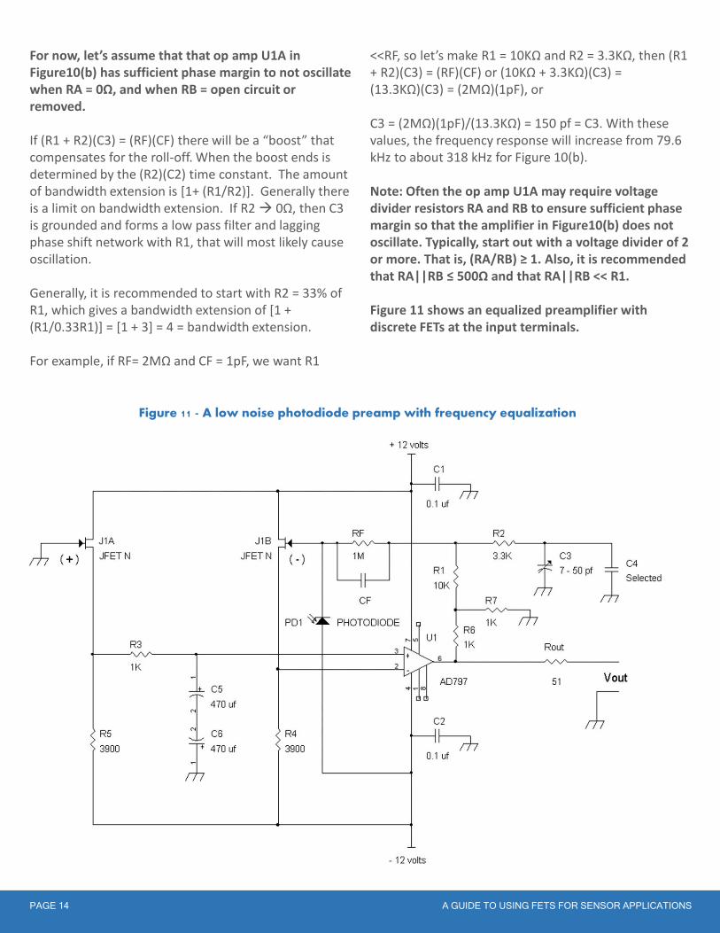
Figure 11 - A low noise photodiode preamp with frequency equalization
In Figure 11 on the previous page, the effective feedback resistor is about 2MΩ because R6 and R7 provide a divide by two voltage divider. The effective feedback resistance is [1 + (R6/R7) ] x RF = [1 +1] x 1MΩ = 2MΩ, given that R1 << RF or 10KΩ << 1MΩ.
J1A and J1B are low noise and low capacitance matched pair JFETs such as the LSK489.
U1 can be typically a bipolar input stage op amp for the lowest equivalent input voltage noise density such as the AD797. Variable trimmer capacitor C3 is adjusted for the flattest frequency response.
Alternatively C3 may be adjusted for the best pulse response. Generally an LED is driven with a square wave signal and is pointed into the photodiode PD1. C3 is adjusted for the fastest rise and fall times while avoiding overshoot at Vout.
In Figure 11, R6 and R7 form a voltage divider to multiply RF for an effective resistance of 2MΩ. But R6 and R7 also adds some series resistance to R1. This series resistance is R6||R7 = 1KΩ||1KΩ = 500Ω, which is the Thevenin resistance from the voltage divider circuit. To calculate the proper time constants for frequency compensation we have:
[(R6||R7) + (R1 + R2)] x [C3 + C4] = RF x CF which leads to:
[C3 + C4] = [RF x CF]/ [(R6||R7) + (R1 + R2)]
For example, in Figure 11, suppose CF = 2.2 pF is the capacitance across RF = 1MΩ.
Also U1 = AD797
[C3 + C4] = [1MΩ x 2.2 pF]/ [(500Ω) + (10KΩ + 3.3KΩ)]
[C3 + C4] = [1MΩ x 2.2 pF]/ [(500Ω) + (13.3KΩ)]
[C3 + C4] = 72.46 x 2.2 pF = 159 pF
Let C4 = 130 pF so that the remaining 29 pF can be set by variable capacitor C3. Note that C3 is adjusted for
best transient or frequency response.
The circuit was built with and without the equalization network, R1, R2, C3, and C4.
Without the equalization network and with CF = 2.2 pF, the – 3 dB measured frequency response was about 71 kHz which matches closely to [1/2π(1MΩ)(2.2 pF)] = 72.5 kHz.
The bandwidth extension is [1 + (R1/R2)] = [1 + (10K/3.3K)] = [1 +3] = 4.
Thus, we will expect the frequency response to be extended to 4 x 72.5 kHz = 290 kHz.
With the equalization network and C4 adjusted, the measured frequency response was extended to > 300 kHz.
Note: When an LT1028 op amp was used instead of the AD797 for U1, R7 had to be reduced to 100Ω to avoid oscillation and to provide sufficient phase margin. Not all op amps will necessarily have the enough phase margin to ensure an oscillation free condition with R6 = R7 in Figure 11. At times R7 may have to be lowered in value for stability, but also keep in mind that the effective feedback resistance is RF x [1 + (R6/R7)].
PAGE 15 A GUIDE TO USING FETS FOR SENSOR APPLICATIONS
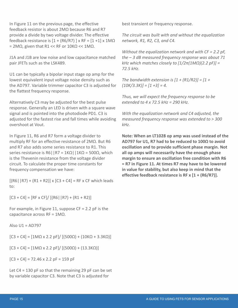
Figure 12 shows an example with a hydrophone amplifier.
In some instances, piezoelectric elements can be amplified with a low noise voltage amplifier instead of a charge amplifier. In this case a hydrophone transducer
or microphone is connected to a source follower circuit J1A and current source Q2A. J1A can be an LSK170 for the lowest noise. Current source circuit R1, LED1, R2, and Q1A may be replaced with a 3900Ω resistor from the source of J1A to – 12 volts.
Specific Applications
Hydrophone Voltage Gain Amplifier
Figure 12 - Hydrophone Amplifier with a gain of 41
PAGE 16 A GUIDE TO USING FETS FOR SENSOR APPLICATIONS
References:
1) “Piezoelectric Transducers”, Dale Pennington, Endevco Dynamic Instrument Division, Rev. 7/70.2) Columbia Research Laboratories, General Purpose Accelerometers, Models 3021,3022, 3023, 5001,
and 5002.3) Columbia Research Laboratories, Dynamic Pressor Sensors, Models P-308-C, P-766, 765M25, and
765M27.4) Kistler Instrument Corporation, Quartz High Resonant Frequency, Charge Mode, Shock Accelerometer,
Type 8044.5) Analog Devices, Data Sheet, AD797.6) Analog Devices, Data Sheet, AD743.7) Linear Technology, Data Sheet, LTC6078.8) Linear Technology, Data Sheet,LT1028.9) Vishay Semiconductors, Data Sheet, BVP10 Silicon PIN Photodiode.
PAGE 17 A GUIDE TO USING FETS FOR SENSOR APPLICATIONS