


Languages
Pages
Legal

ANSYS HFSS 3D Layout
侯明刚
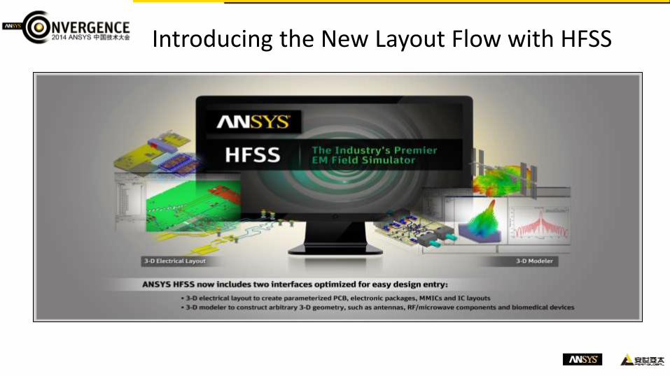
Introducing the New Layout Flow with HFSS
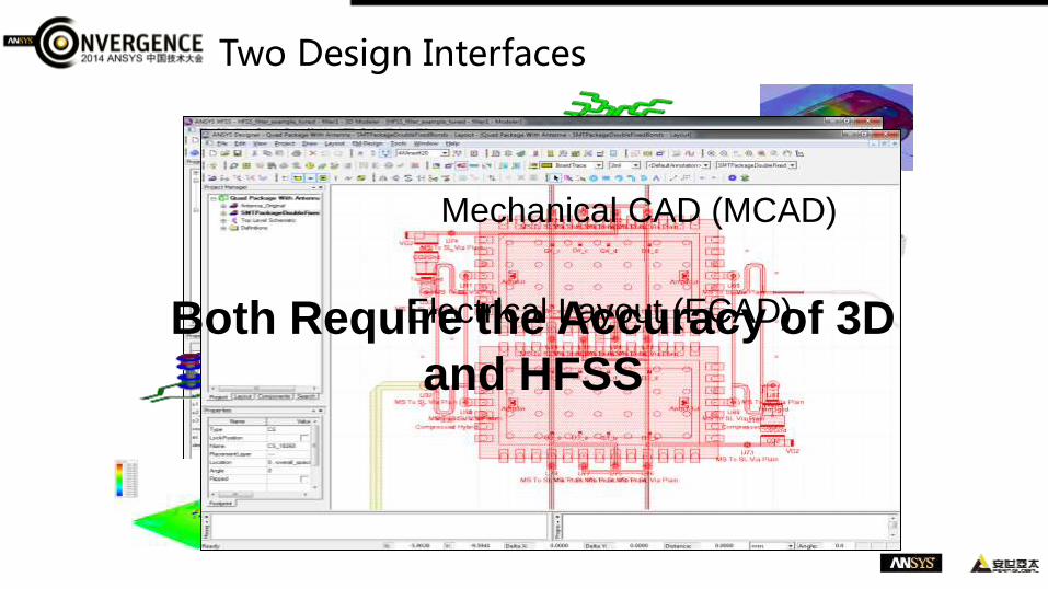
Two Design Interfaces
Both Require the Accuracy of 3D
and HFSS
Mechanical CAD (MCAD)
Electrical Layout (ECAD)
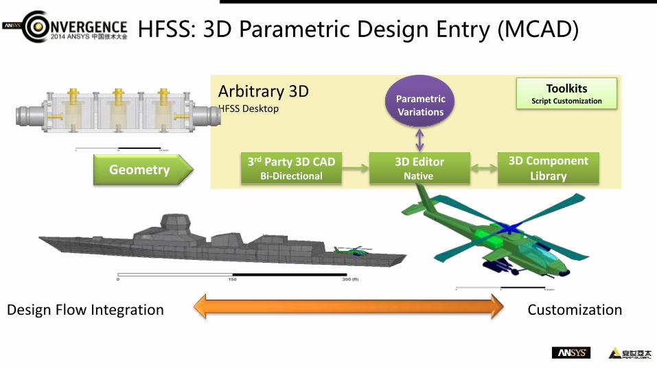
HFSS: 3D Parametric Design Entry (MCAD)
Geometry 3rd Party 3D CAD
Bi-Directional
Toolkits Script Customization
3D Component Library
Design Flow Integration Customization
3D Editor Native
Arbitrary 3D HFSS Desktop
Parametric Variations

HFSS: Layout Parametric Design Entry (EDA)
Geometry Layout Editor
Native
Toolkits Script Customization
Scripted Footprints
3rd Party Layout Translation
‘3D’ Layout Designer Desktop
Parametric Variations
Design Flow Integration Customization

HFSS v2014: Arbitrary 3D or 3D Layout
• No change to 3D product, licenses added to enable layout – ensemble_gui – nexxim_gui
• Required Installs – HFSS v2014 – Designer v2014
3rd Party 3D CAD Bi-Directional
3D Component Library
3D Editor Native
Scripted Footprints
3rd Party Layout Translation
Arbitrary 3D
3D Layout
Layout Editor Native
Toolkits Script Customization
Toolkits Script Customization Parametric
Variations
Parametric Variations
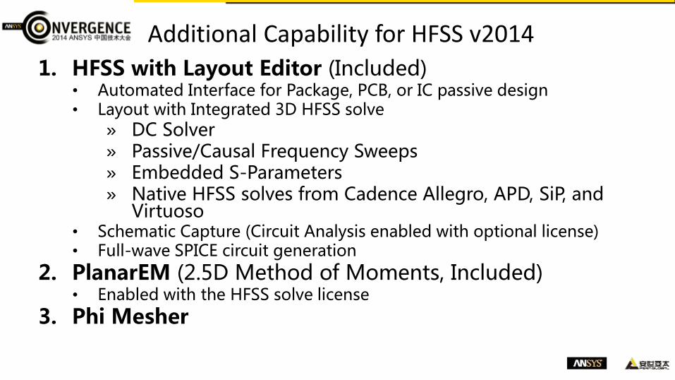
Additional Capability for HFSS v2014
1. HFSS with Layout Editor (Included) • Automated Interface for Package, PCB, or IC passive design • Layout with Integrated 3D HFSS solve
» DC Solver » Passive/Causal Frequency Sweeps » Embedded S-Parameters » Native HFSS solves from Cadence Allegro, APD, SiP, and
Virtuoso • Schematic Capture (Circuit Analysis enabled with optional license) • Full-wave SPICE circuit generation
2. PlanarEM (2.5D Method of Moments, Included) • Enabled with the HFSS solve license
3. Phi Mesher

• Features for HFSS from Layout – Integrated HFSS for layout geometry – Parametric Layout Editor
• Stackup – Etch Factor/Layer Offset • Padstacks • Trace parameters • HFSS Extents • Finite Dielectrics • Sub-region • Hierarchy
– Solver • Integrated HFSS solver • DC Solver • Embedded RLC and/or S-Parameters for HFSS
– Post-Processing • Network Data Explorer • Full-Wave SPICE/HSPICE broadband ROM export
– Integration with industry: • Cadence, Zuken, Mentor and Altium
HFSS from Layout

• Now included with HFSS
• Fast solve – 2D conductors – Infinite GND – Early in the
design process
• Leverage HFSS and 3D FEM with adaptive meshing in the later stages
PlanarEM 2.5D Method of Moments
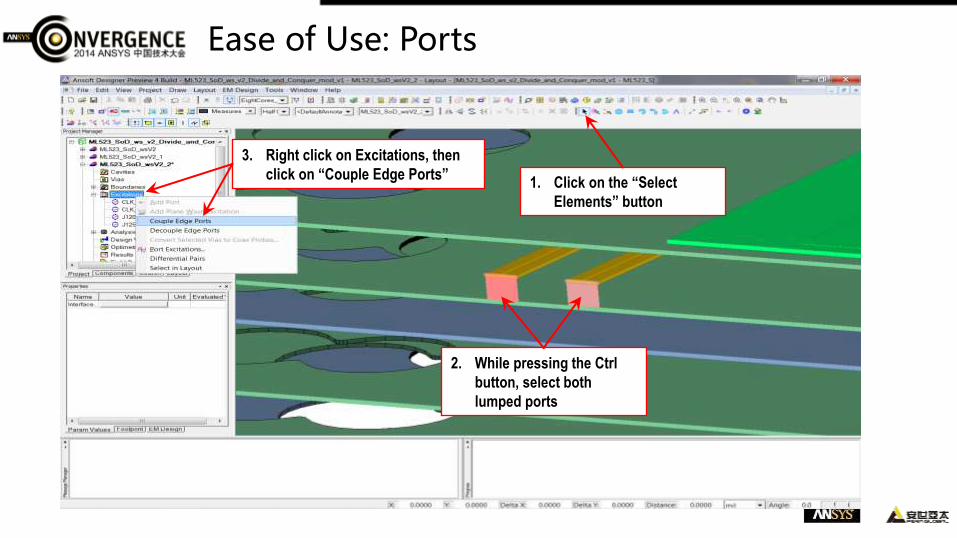
Ease of Use: Ports
1. Click on the “Select
Elements” button
2. While pressing the Ctrl
button, select both
lumped ports
3. Right click on Excitations, then
click on “Couple Edge Ports”

Convert to Differential Waveport in One Click
Newly created coupled Waveport
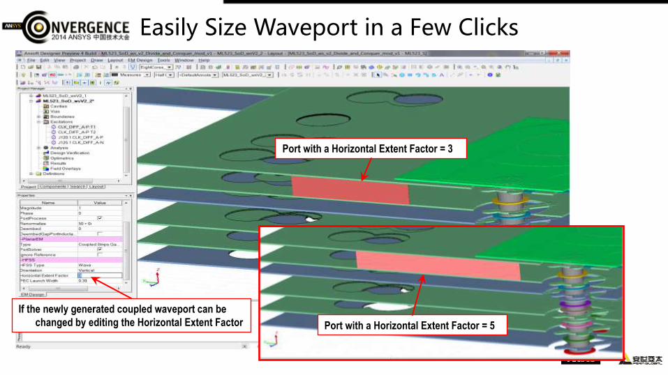
Easily Size Waveport in a Few Clicks
Port with a Horizontal Extent Factor = 3
Port with a Horizontal Extent Factor = 5
If the newly generated coupled waveport can be
changed by editing the Horizontal Extent Factor

HFSS Solve from SIwave

– Create and Solve HFSS models from within • Allegro® Package Designer
• Allegro® PCB Designer
• SiP Digital Layout
• Virtuoso® Analog Design Environment
HFSS within Cadence
Set-up and solve HFSS
simulations without
leaving the Cadence
environment

HFSS 3D Layout and the Phi Mesher
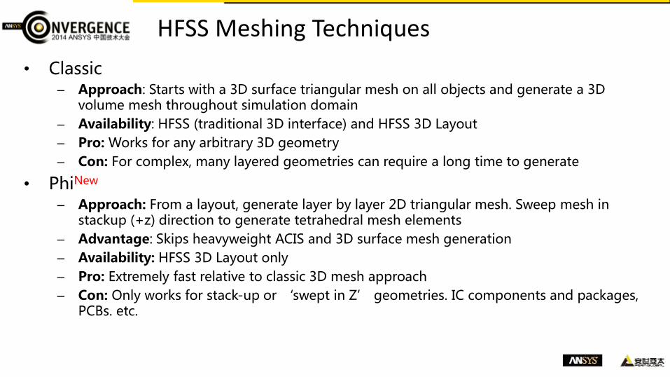
HFSS Meshing Techniques
• Classic – Approach: Starts with a 3D surface triangular mesh on all objects and generate a 3D
volume mesh throughout simulation domain
– Availability: HFSS (traditional 3D interface) and HFSS 3D Layout
– Pro: Works for any arbitrary 3D geometry
– Con: For complex, many layered geometries can require a long time to generate
• PhiNew
– Approach: From a layout, generate layer by layer 2D triangular mesh. Sweep mesh in stackup (+z) direction to generate tetrahedral mesh elements
– Advantage: Skips heavyweight ACIS and 3D surface mesh generation
– Availability: HFSS 3D Layout only
– Pro: Extremely fast relative to classic 3D mesh approach
– Con: Only works for stack-up or ‘swept in Z’ geometries. IC components and packages, PCBs. etc.
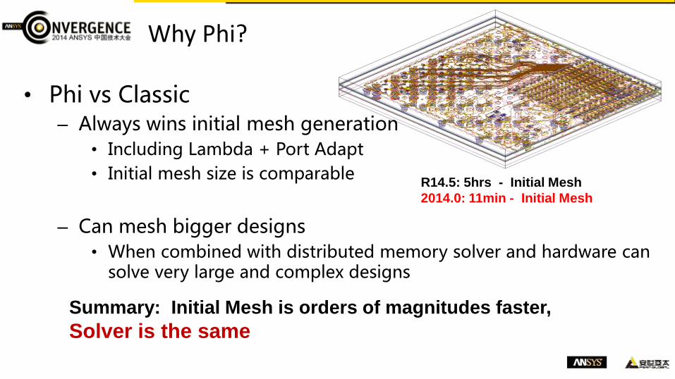
Why Phi?
• Phi vs Classic – Always wins initial mesh generation
• Including Lambda + Port Adapt
• Initial mesh size is comparable
– Can mesh bigger designs • When combined with distributed memory solver and hardware can
solve very large and complex designs
Summary: Initial Mesh is orders of magnitudes faster,
Solver is the same
R14.5: 5hrs - Initial Mesh
2014.0: 11min - Initial Mesh
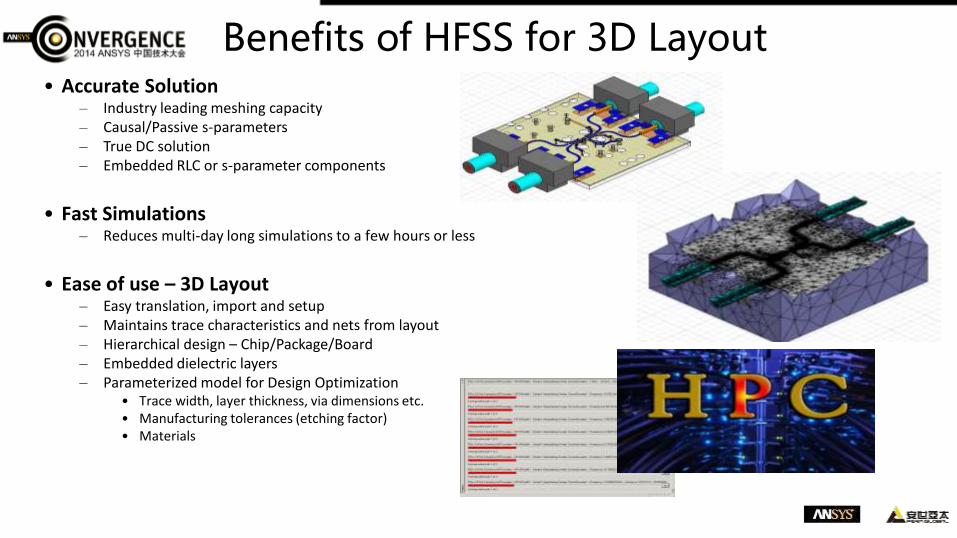
• Accurate Solution – Industry leading meshing capacity – Causal/Passive s-parameters – True DC solution – Embedded RLC or s-parameter components
• Fast Simulations
– Reduces multi-day long simulations to a few hours or less
• Ease of use – 3D Layout
– Easy translation, import and setup – Maintains trace characteristics and nets from layout – Hierarchical design – Chip/Package/Board – Embedded dielectric layers – Parameterized model for Design Optimization
• Trace width, layer thickness, via dimensions etc. • Manufacturing tolerances (etching factor) • Materials
Benefits of HFSS for 3D Layout
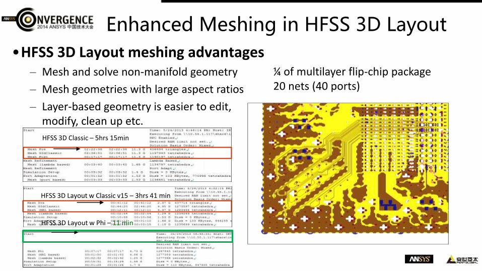
HFSS 3D Classic – 5hrs 15min
HFSS 3D Layout w Classic v15 – 3hrs 41 min
•HFSS 3D Layout meshing advantages – Mesh and solve non-manifold geometry
– Mesh geometries with large aspect ratios
– Layer-based geometry is easier to edit, modify, clean up etc.
Enhanced Meshing in HFSS 3D Layout
¼ of multilayer flip-chip package 20 nets (40 ports)
HFSS 3D Layout w Phi – 11 min

Is there a difference between
HFSS 3D and HFSS 3D Layout ?
Solve a model in both HFSS 3D and HFSS 3D Layout and compare
Note easy export from HFSS 3D layout to HFSS 3D
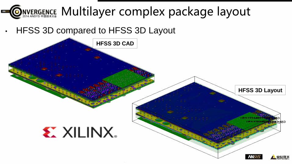
Multilayer complex package layout
• HFSS 3D compared to HFSS 3D Layout
HFSS 3D CAD
HFSS 3D Layout

Initial Meshing Comparison • Extremely fast initial Phi meshing. Phi is 20X faster!
• 4min vs. 1hr 20min
HFSS 3D - Classic
HFSS 3D Layout - PHI

HFSS 3D – Run Time
• Total: 6hrs 33min
• Adaptive Part: 4hr 1min
• Interpolating Sweep: 2hrs 32 min
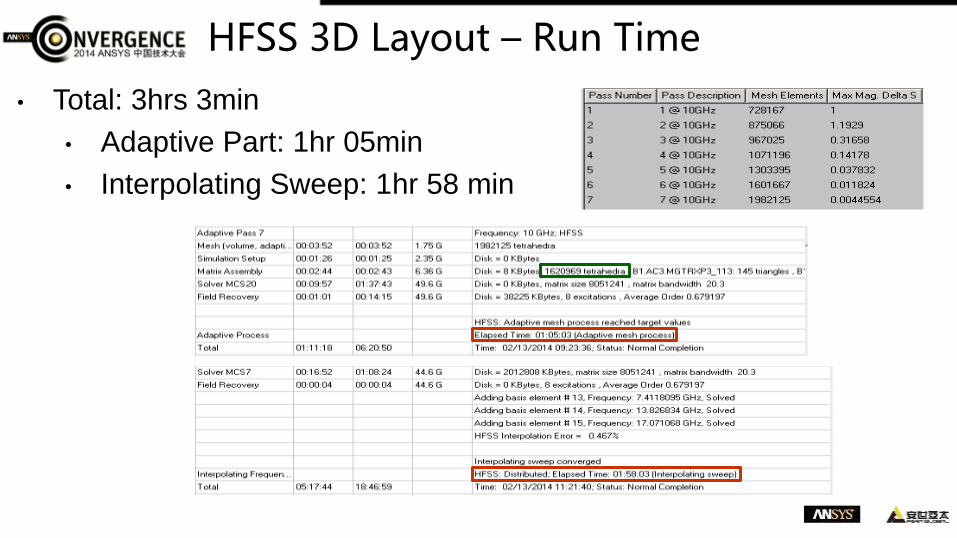
HFSS 3D Layout – Run Time
• Total: 3hrs 3min
• Adaptive Part: 1hr 05min
• Interpolating Sweep: 1hr 58 min
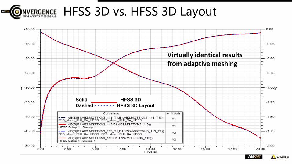
HFSS 3D vs. HFSS 3D Layout
Solid HFSS 3D
Dashed - - - - - - - HFSS 3D Layout
Virtually identical results from adaptive meshing

Summary
HFSS 3D CAD HFSS 3D Layout
Initial Mesher Classic Phi
Initial Mesh Size (tets) 763, 953 712, 536
Initial Mesh Time 1hr 20min 4min
Number of Adaptive Passes 6 7
Number of Tets - Final 1, 617, 954 1, 620, 969
Adaptive Passes Run Time 4hrs 1min 1hr 5min (3.7X faster)
RAM 47.6 GB 49.6 GB
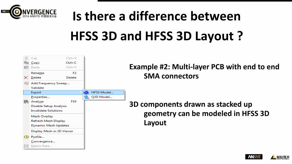
Is there a difference between
HFSS 3D and HFSS 3D Layout ?
Example #2: Multi-layer PCB with end to end SMA connectors
3D components drawn as stacked up geometry can be modeled in HFSS 3D Layout
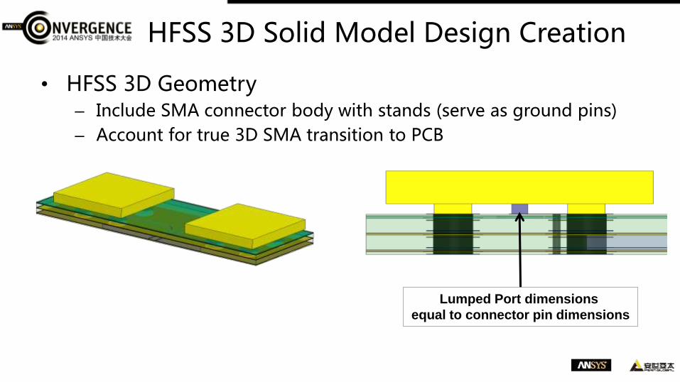
• HFSS 3D Geometry – Include SMA connector body with stands (serve as ground pins)
– Account for true 3D SMA transition to PCB
HFSS 3D Solid Model Design Creation
Lumped Port dimensions
equal to connector pin dimensions

• Added SMA body geometry to a layout stackup
• Port properties created automatically
HFSS 3D Layout Design Creation
Layout View
EM Design 3D View
Stackup Editor Port/pin settings
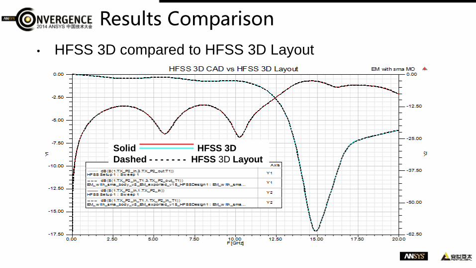
Results Comparison
• HFSS 3D compared to HFSS 3D Layout
Solid HFSS 3D
Dashed - - - - - - - HFSS 3D Layout

• Phi meshing是突破性的有限元网格生成技术。
• 为IC、IC封装和PCB设计者提供了电路工程师熟悉的操作界面和快速初始网格刨分和快速仿真技术。
• 结合ANSYS HPC技术增加求解规模的可扩展性,支持求解更大、更复杂的层叠结构。
• 分布式直接矩阵求解器(Distributed direct matrix solver)使用多机分布式内存方式求解及其消耗内存的超大型复杂设计。
• 频域分解算法(Spectral decomposition method) 进行多频点并行求解,加快扫频速度。
总结

Top Related