Working X3T13 Draft 2008D - Stanford University · Working X3T13 Draft 2008D Revision 7b ... 2190...
182
Working X3T13 Draft 2008D Revision 7b 27 January 1997 Information Technology - AT Attachment-3 Interface (ATA-3) This is a draft proposed American National Standard of Accredited Standards Committee X3. As such it is not a completed standard. The X3T13 Technical Committee may modify this document as a result of comments received during the review process. Permission is granted to members of X3, its technical committees, and their associated task groups to reproduce this document for the purposes of X3 standardization activities without further permission, provided this notice is included. All other rights are reserved. Any commercial or for-profit replication or republication is prohibited. X3T13 Technical Editor: Peter T. McLean Maxtor Corporation 2190 Miller Drive Longmont, CO 80501-6744 USA Tel: 303-678-2149 Fax: 303-682-4811 Email: [email protected] Reference number ANSI X3.298 - 1997 Printed January, 17, 1997 12:09PM
Transcript of Working X3T13 Draft 2008D - Stanford University · Working X3T13 Draft 2008D Revision 7b ... 2190...

Working X3T13Draft 2008D
Revision 7b27 January 1997
Information Technology -AT Attachment-3 Interface(ATA-3)
This is a draft proposed American National Standard of Accredited Standards Committee X3. As such it isnot a completed standard. The X3T13 Technical Committee may modify this document as a result ofcomments received during the review process.
Permission is granted to members of X3, its technical committees, and their associated task groups toreproduce this document for the purposes of X3 standardization activities without further permission,provided this notice is included. All other rights are reserved. Any commercial or for-profit replication orrepublication is prohibited.
X3T13 Technical Editor:Peter T. McLeanMaxtor Corporation2190 Miller DriveLongmont, CO 80501-6744USA
Tel: 303-678-2149Fax: 303-682-4811Email: [email protected]
Reference numberANSI X3.298 - 1997
Printed January, 17, 1997 12:09PM

X3T13/2008D Revision 7b
working draft AT Attachment-3 (ATA-3)
Other Points of Contact:
X3T13 Chair X3T13 Vice-ChairGene Milligan Pete McLeanSeagate Technology Maxtor CorporationOKM 251 2190 Miller Drive10323 West Reno (West Dock) Longmont, CO 80501P.O. Box 12313 Tel: 303-678-2149Oklahoma City, OK 73157-2313 Fax: 303-682-4811Tel: 405-324-3070 E-mail: [email protected]: 405-324-3794E-mail: [email protected]
X3 SecretariatLynn BarraAdministrator Standards ProcessingX3 Secretariat1250 Eye Street, NW Suite 200Washington, DC 20005Tel: 202-626-5738Fax: 202-638-4922Email: [email protected]
ATA ReflectorInternet address for subscription to the ATA reflector: [email protected] email to above account and include in BODY of text, on a line by itself the following:
"subscribe ata [your email address]"Internet address for distribution via ATA reflector: [email protected]
ATA Anonymous FTP Sitefission.dt.wdc.comATA directory is: "/pub/standards/X3T13"
Document DistributionGlobal Engineering15 Inverness Way EastEnglewood, CO 80112-5704Tel: 303-792-2181 or 800-854-7179Fax: 303-792-2192

X3T13/2008D Revision 7b
working draft AT Attachment-3 (ATA-3)
DOCUMENT STATUS
Revision 0 - 28 February 1995
Initial document. Created from X3T10/948D Revision 2k, the proposed AT Attachment Interfacewith Extensions (ATA-2) standard, and the following proposed additions:
X3T10/94-053r3 Reset Pulse DurationX3T10/94-087r3 Security ModeX3T10/94-154r1 Check Power Mode EnhancementX3T10/95-144r0 Identify Device DMAX3T10/95-145r0 Device 1 Only
It is the intent of the editor that any changes that may be made to X3T10/948D by the X3T10 beimplemented in this document as well. In addition, the editor has taken the liberty to makeimprovements as deemed necessary, understanding that the entire document is subject to reviewand change.
Revision 1 - 21 April 1995
Added changes made to X3T10/948D Revision 3 as a result of letter ballot. Rewrote Abstract,Introduction and Scope. Added the proposals approved at the April 12-13, 1995 meeting as follows:
X3T10/95-125r2 Dynamic Power SelectionX3T10/95-155r0 Delete DASP timing clause 10.6X3T10/95-198r0 DRDY max set time 30 secX3T10/95-198r0 Paragraph merge in READ MULTIPLE commandX3T10/95-199r0 Modify driver current
Revision 2 - 2 June 1995
Added proposal X3T10/95-154r1 and 10K pulldown to DD7 as approved at the 11 May 1995meeting.
Revision 3 - 26 July 1995
Per the June 21-22 working group meeting:Corrected reset timing figuresAdded FFh not specified in revision word.Removed word “non-shielded” from Clause 5.1.
Per the July 18-20 working group meeting:Added ATAPI bit definition in word 1 of DEVICE ID response.Removed DEVICE ID response word 71.Moved DEVICE ID response words 72 and 73 to words 73 and 74.Added SFF8035i S.M.A.R.T. into the standard.Added X3T10/95-294r0, Set Features changes into document.Reformatted protocol diagrams.Added DD7 pull-down modification.Deleted Annex A, reset considerations.Moved 40-pin connector definition into new Annex A that includes other connector definitionspreviously in Annex B and C.Deleted the IOCS16- signal.Deleted WRITE SAME command.Made numerous other minor changes requested during page-by-page review.

X3T13/2008D Revision 7b
working draft AT Attachment-3 (ATA-3)
Revision 4 - 6 September 1995
Per the August 22-25 working group meeting:Changed capacitance values in table 4.Modified cable configuration in clause 4.1 and figure 2.Removed 8-bit transfer mode.Added bibliography.Made LBA mandatory.Made READ, WRITE, and SET MULTIPLE mandatory.Removed single word DMA.Made READ and WRITE DMA mandatory.Inserted tables into command code definitions.Made SET FEATURES mandatory.Made numerous other changes requested during page-by-page review.
Revision 5 - 6 October 1995
Per the September 19-22 working group meeting:Added text to clause 6.2.Changed security mode definition to X3T10/95-329r0Added text to READ/WRITE LONGChanged protocol flowcharts to X3T10/95-330r1.Added X3T10/95-331r0 to clause 7.4.Deleted ACKNOWLEDGE MEDIA CHANGE, POST BOOT AND PRE BOOT COMMANDS.Added signal integrity annex C, (modified SFF 8036I)Made numerous other changes requested during page-by-page review.Made editorial changes requested by the ANSI editor for ATA-2 document.
Revision 6 - 26 October 1995
Per the October 17-19 working group meeting:Added command set supported, words 82-83, to IDENTIFY DEVICE response.Deleted Bxh codes for security mode.Made numerous other changes requested during page-by-page review.
Revision 7 - 25 April 1996
Resolution of letter ballot comments added per X3T13/D96112r2.
Revision 7a - 18 September 1996
Added editorial changes recommended by ANSI pre-edit.Added public review comment restoring register transfer timing.
Revision 7b - 27 January 1997
Added X3 letter ballot comment changing DMARQ to DMACK- in clauses 5.2.2, 5.2.3, 5.2.4, 5.2.5, 5.2.6,5.2.7, 5.2.8, 5.2.10, 5.2.11 and 5.2.12.

X3T13/2008D Revision 7b
working draft AT Attachment-3 (ATA-3)
ANSI®
X3.298-1997
American National Standardfor Information Systems
AT Attachment-3 Interface (ATA-3)
SecretariatInformation Technology Industry Council
Approved mm dd yy
American National Standards Institute, Inc.
Abstract
This standard specifies the AT Attachment Interface between host systems and storage devices. It providesa common attachment interface for systems manufacturers, system integrators, software suppliers, andsuppliers of intelligent storage devices.
This standard maintains a high degree of compatibility with the AT Attachment Interface with Extensionsstandard (ATA-2), X3.279-1996, and while providing additional functions, is not intended to require changesto presently installed devices or existing software.

X3T13/2008D Revision 7b
working draft AT Attachment-3 (ATA-3)
AmericanNationalStandard
Approval of an American National Standard requires verification by ANSI that therequirements for due process, consensus, and other criteria for approval have beenmet by the standards developer. Consensus is established when, in the judgment ofthe ANSI Board of Standards Review, substantial agreement has been reached bydirectly and materially affected interests. Substantial agreement means much morethan a simple majority, but not necessarily unanimity. Consensus requires that allviews and objections be considered, and that effort be made towards theirresolution.
The use of American National Standards is completely voluntary; their existencedoes not in any respect preclude anyone, whether he has approved the standards ornot, from manufacturing, marketing, purchasing, or using products, processes, orprocedures not conforming to the standards.
The American National Standrads Institute does not develop standards and will inno circumstances give interpretation on any American National Standard. Moreover,no person shall have the right or authority to issue an interpretation of an AmericanNational Standard in the name of the American National Standards Institute.Requests for interpretations should be addressed to the secretariat or sponsorwhose name appears on the title page of this standard.
CAUTION NOTICE: This American National Standard may be revised orwithdrawn at any time. The procedures of the American National Standards Instituterequire that action be taken periodically to reaffirm, revise, or withdraw thisstandard. Purchasers of American National Standards may receive currentinformation on all standards by calling or writing the American National StandardsInstitute.
CAUTION: The developers of this standard have requested that holders of patents that may be required forthe implementation of the standard, disclose such patents to the publisher. However, neither thedevelopers nor the publisher have undertaken a patent search in order to identify which, if any, patents mayapply to this standard.
As of the date of publication of this standard, following calls for the identification of patents that may berequired for the implementation of the standard, notice of one or more claims has been received.
By publication of this standard, no position is taken with respect to the validity of this claim or of any rights inconnection therewith. The patent holders have, however, filed a statement of willingness to grant a licenseunder these rights on reasonable and nondiscriminatory terms and conditions to applicants desiring toobtain such a license. Details may be obtained from the publisher.
No further patent search is conducted by the developer or the publisher in respect to any standard itprocesses. No representation is made or implied that licenses are not required to avoid infringement in theuse of this standard.
Published byAmerican National Standards Institute11 West 42nd Street, New York, New York 10036
Copyright 1997 by American National Standards InstituteAll rights reserved.

X3T10/2008D Revision 7b
working draft AT Attachment-3 (ata-3) Page i
Contents Page
Foreword .............................................................................................................................................ivIntroduction..........................................................................................................................................vii1 Scope...............................................................................................................................................12 Definitions, abbreviations, and conventions.......................................................................................2
2.1 Definitions and abbreviations..................................................................................................22.2 Conventions ...........................................................................................................................3
3 Interface physical and electrical requirements ...................................................................................63.1 Cable configuration ................................................................................................................63.2 I/O cable ................................................................................................................................63.3 Electrical characteristics.........................................................................................................7
4 Interface signal assignments and descriptions ..................................................................................94.1 Signal summary .....................................................................................................................94.2 Signal descriptions .................................................................................................................9
5 Interface register definitions and descriptions....................................................................................135.1 Device addressing considerations ..........................................................................................135.2 I/O register descriptions .........................................................................................................13
6 General operational requirements .....................................................................................................296.1 Reset response......................................................................................................................296.2 Sector addressing ..................................................................................................................296.3 Power management feature set..............................................................................................306.4 Removable media mode transitions........................................................................................326.5 Security mode feature set ......................................................................................................336.6 Self-monitoring, analysis, and reporting technology ................................................................36
7 Command descriptions .....................................................................................................................387.1 CHECK POWER MODE ........................................................................................................407.2 DOOR LOCK .........................................................................................................................417.3 DOOR UNLOCK ....................................................................................................................427.4 DOWNLOAD MICROCODE...................................................................................................437.5 EXECUTE DEVICE DIAGNOSTIC.........................................................................................447.6 FORMAT TRACK...................................................................................................................477.7 IDENTIFY DEVICE ................................................................................................................487.8 IDENTIFY DEVICE DMA .......................................................................................................587.9 IDLE ......................................................................................................................................597.10 IDLE IMMEDIATE................................................................................................................607.11 INITIALIZE DEVICE PARAMETERS....................................................................................617.12 MEDIA EJECT .....................................................................................................................627.13 NOP.....................................................................................................................................637.14 READ BUFFER....................................................................................................................647.15 READ DMA (with retries and without retries) ........................................................................657.16 READ LONG (with retries and without retries) ......................................................................667.17 READ MULTIPLE ................................................................................................................677.18 READ SECTOR(S) (with retries and without retries).............................................................697.19 READ VERIFY SECTOR(S) (with retries and without retries) ...............................................707.20 RECALIBRATE....................................................................................................................717.21 SECURITY DISABLE PASSWORD .....................................................................................727.22 SECURITY ERASE PREPARE ............................................................................................737.23 SECURITY ERASE UNIT.....................................................................................................747.24 SECURITY FREEZE LOCK .................................................................................................757.25 SECURITY SET PASSWORD .............................................................................................767.26 SECURITY UNLOCK ...........................................................................................................787.27 SEEK...................................................................................................................................797.28 SET FEATURES..................................................................................................................80
X3T13/2008D Revision 7b
Page ii working draft AT Attachment-3 (ATA -3)
Contents Page
7.29 SET MULTIPLE MODE........................................................................................................847.30 SLEEP.................................................................................................................................857.31 SMART................................................................................................................................867.32 STANDBY............................................................................................................................977.33 STANDBY IMMEDIATE .......................................................................................................987.34 WRITE BUFFER..................................................................................................................997.35 WRITE DMA (with retries and without retries).......................................................................1007.36 WRITE LONG (with retries and without retries) ....................................................................1017.37 WRITE MULTIPLE...............................................................................................................1027.38 WRITE SECTOR(S) (with retries and without retries) ...........................................................1047.39 WRITE VERIFY ...................................................................................................................105
8 Protocol ............................................................................................................................................1068.1 Power on and hardware resets...............................................................................................1068.2 Software reset........................................................................................................................1078.3 PIO data in commands...........................................................................................................1098.4 PIO data out commands.........................................................................................................1128.5 Non-data commands..............................................................................................................1158.6 DMA data transfer commands................................................................................................1178.7 Single device configurations ...................................................................................................120
9 Timing ..............................................................................................................................................1229.1 Deskewing .............................................................................................................................1229.2 Symbols.................................................................................................................................1229.3 Terms ....................................................................................................................................1229.4 Data transfers ........................................................................................................................122
Tables Page
1 Byte order........................................................................................................................................52 DC characteristics ...........................................................................................................................73 AC characteristics............................................................................................................................74 Driver types and required termination...............................................................................................85 Interface signal name assignments ..................................................................................................96 I/O port functions and selection addresses.......................................................................................147 Security mode command actions .....................................................................................................358 Diagnostic codes .............................................................................................................................449 Identify device information ...............................................................................................................4910 Minor revision number ...................................................................................................................5611 Automatic standby timer periods ....................................................................................................5912 Security password content.............................................................................................................7213 SECURITY SET PASSWORD data content...................................................................................7614 Identifier and security level bit interaction.......................................................................................7715 SET FEATURES register definitions ..............................................................................................8116 Transfer/mode values ....................................................................................................................8117 Device attribute thresholds data structure ......................................................................................9118 Individual threshold data structure..................................................................................................9119 Device attributes data structure .....................................................................................................9320 Individual attribute data structure ...................................................................................................9321 Register transfer to/from device ......................................................................................................12522 PIO data transfer to/from device ....................................................................................................12723 Multiword DMA data transfer..........................................................................................................129

X3T13/2008D Revision 7b
working draft AT Attachment-3 (ATA-3) Page iii
Figures Page
1 ATA interface cabling diagram .........................................................................................................62 Cable select example.......................................................................................................................123 Power management modes .............................................................................................................314 Removable modes...........................................................................................................................325 Password set security mode power-on flow......................................................................................346 User password lost ..........................................................................................................................347 BSY and DRDY timing for diagnostic command...............................................................................468 BSY and DRDY timing for power on and hardware resets................................................................1079 BSY and DRDY timing for software reset.........................................................................................10910 Example of PIO data transfer in diagram .......................................................................................11011 Example of PIO data transfer out diagram .....................................................................................11312 Example of non-data transfer diagram ...........................................................................................11613 Example of DMA data transfer diagram .........................................................................................11814 Register transfer to/from device ......................................................................................................12415 PIO data transfer to/from device ....................................................................................................12616 Multiword DMA data transfers........................................................................................................128
Annexes Page
A Connectors ......................................................................................................................................130B Identify device data for ATA devices below 8 GB .............................................................................138C Signal integrity .................................................................................................................................141D Bibliography .....................................................................................................................................163E ATA command set summary ............................................................................................................164

X3T13/2008D Revision 7b
Page iv working draft AT Attachment-3 (ATA -3)
Foreword(This foreward is not part of American National Standard X3.298-1997.)
This AT Attachment-3 Interface (ATA-3) standard is designed to maintain a high degree of compatibility withthe AT Attachment Interface with Extensions standard (ATA-2), while providing the advantages of additionalfeatures and functions.
This standard was developed by the ATA/ATAPI ad hoc working group of X3T10 during 1994-1995. Thestandards approval process started in 1995. This document was transferred to X3T13 in January 1996. Thisdocument includes five annexes. Annex A is normative, and Annexes B to E are informative and are notconsidered part of the standard.
Requests for interpretation, suggestions for improvement and addenda, or defect reports are welcome. Theyshould be sent to the X3 Secretariat, Information Technology Industry Council, 1250 Eye Street, NW, Suite200, Washington, DC 20005-3922.
This standard was processed and approved for submittal to ANSI by Accredited Standards Committee onInformation Processing Systems, X3. Committee approval of the standard does not necessarily imply that allcommittee members voted for approval. At the time it approved this standard, the X3 Committee had thefollowing members:
James D. Converse, Chairman
Donald C. Loughry, Vice-Chairman
Joanne M. Flanagan, Secretary
Organization Represented .......................................................................Name of RepresentativeAmerican Nuclear Society........................................................................Geraldine C. Main
Sally Hartzell (Alt.)AMP, Inc .................................................................................................Edward Kelly
Charles Brill (Alt.)Apple Computer.......................................................................................Karen HigginbottomAssociation of the Institute for Certification of Professionals (AICCP).......Kennath ZemrowskiAT&T/NCR ..............................................................................................Thomas W. Kern
Thomas F. Frost (Alt.)Boeing Company .....................................................................................Catherine Howells
Andrea Vanosdoll (Alt.)Bull HN Information Systems, Inc. ...........................................................William GeorgeCompaq Computer Corporation ...............................................................James BarnesDigital Equipment Corporation .................................................................Delbert Shoemaker
Kevin Lewis (Alt.)Eastman Kodak .......................................................................................James D. Converse
Michael Nier (Alt.)GUIDE International.................................................................................Frank Kirshenbaum
Harold Kuneke (Alt.)Hewlett-Packard ......................................................................................Donald C. LoughryHitachi America, Ltd.................................................................................John Neumann
Kei Yamashita (Alt.)Hughes Aircraft Company........................................................................Harold L. ZebrackIBM Corporation ......................................................................................Joel Urman
Mary Anne Lawler (Alt.)National Communication Systems............................................................Dennis BodsonNational Institute of Standards and Technology .......................................Robert E. Roundtree
Michael Hogan (Alt.)Northern Telecom, Inc. ............................................................................Mel Woinsky
Subhash Patel (Alt.)

X3T13/2008D Revision 7b
working draft AT Attachment-3 (ATA-3) Page v
Neville & Associates ................................................................................Carlton NevilleRecognition Technology Users Association..............................................Herbert P. Schantz
G. Edwin Hale (Alt.)Share, Inc................................................................................................Gary Ainsworth
David Thewlis (Alt.)Sony Corporation.....................................................................................Michael DeeseStorage Technology Corporation..............................................................Joseph S. Zajaczkowski
Samuel D. Cheatham (Alt.)Sun Microsystems ...................................................................................Scott Jameson
Gary Robinson (Alt.)3M Company ...........................................................................................Eddie T. Morioka
Paul D. Jahnke (Alt.)Unisys Corporation ..................................................................................John L. Hill
Stephen P. Oksala (Alt.)U.S. Department of Defense....................................................................William C. Rinehuls
C. J. Pasquariello (Alt.)U.S. Department of Energy......................................................................Alton Cox
Lawrence A. Wasson (Alt.)U.S. General Services Administration ......................................................Douglas Arai
Larry L. Jackson (Alt.)Wintergreen Information Services ............................................................Joun WheelerXerox Corporation....................................................................................Dwight McBain
Roy Peirce (Alt.)
Subcommittee X3T10 on I/O Interfaces, which reviewed this standard, had the following members:
John B. Lohmeyer, Chairman
Lawrence J. Lamers, Vice-Chairman
Ralph Weber, Secretary
Paul D. AloisiRon AptGeoffrey BartonRobert BellinoCharles BrillMichael BryanJoe ChenChris D'IorioJoe DambachJan V. DedekStephen G. FinchEdward FongLouis GranthamKenneth J. HallamNorm HarrisEdward HaskeStephen F. HeilStephen HolmsteadPeter JohanssonGerry JohnsenSkip JonesEdward LappinRobert LiuBob MastersonDavid McFaddenJames McGrathPete McLean
Patrick MercerGene MilliganCharles MoniaIan MorrellJohn MoyS. NadershahiErich OettingAlan R. OlsonDennis PakDuncan PenmanGeorge PenokieDoug PiperRobert ReischRobert N. SnivelyJeff StaiGary R. StephensClifford E. Strang Jr.Dennis Van DalsenSteven WalkerDean WallaceGary M. WatsonMichael WingardDavid Andreatta (Alt.)Tak Asami (Alt.)Akram Atallah (Alt.)Wayne Baldwin (Alt.)Rick Bohn (Alt.)
Paul Boulay (Alt.)John Cannon (Alt.)Kurt Chan (Alt.)Shufan Chan (Alt.)Ting Li Chan (Alt.)Andy Chen (Alt.)Jack Chen (Alt.)Nancy Cheng (Alt.)Mike Chennery (Alt.)Dan Colegrove (Alt.)Roger Cummings (Alt.)Zane Daggett (Alt.)William Dallas (Alt.)Brian N. Davis (Alt.)Dhiru N. Desai (Alt.)Mike Eneboe (Alt.)Mark Evans (Alt.)Timothy Feldman (Alt.)John Geldman (Alt.)Raymond Gilson (Alt.)Chuck Grant (Alt.)Dave Guss (Alt.)Peter Haas (Alt.)Douglas Hagerman (Alt.)William Ham (Alt.)Tom Hanan (Alt.)Rick Heidick (Alt.)

X3T13/2008D Revision 7b
Page vi working draft AT Attachment-3 (ATA -3)
Gerald Houlder (Alt.)Paul Jackson (Alt.)Kevin James (Alt.)Richard Kalish (Alt.)Greg Kapraun (Alt.)Thomas J. Kulesza (Alt.)Dennis Lang (Alt.)Pat LaVarre (Alt.)Florey Lin (Alt.)Bill Mable (Alt.)John Masiewicz (Alt.)Akira James Miura (Alt.)E.J. Mondor (Alt.)
Jay Neer (Alt.)Marc A. Noblitt (Alt.)Tim Norman (Alt.)Vit Novak (Alt.)Kevin R. Pokorney (Alt.)Gary Porter (Alt.)Steven Ramberg (Alt.)Ron Roberts (Alt.)John P. Scheible (Alt.)J. R. Sims (Alt.)Michael Smith (Alt.)Arlan P. Stone (Alt.)
George Su (Alt.)Nicos Syrimis (Alt.)Matt Thomas (Alt.)Pete Tobias (Alt.)Joseph Wach (Alt.)Roger Wang (Alt.)Bob Whiteman (Alt.)Jeffrey L. Williams (Alt.)Devon Worrell (Alt.)Anthony Yang (Alt.)Danny Yeung (Alt.)Ruben Yomtoubian (Alt.)
Subcommittee X3T13 on ATA interfaces, which reviewed this standard, had the following members:
G. E. Milligan, Chairman
Peter T. McLean, Vice-Chairman
Lawrence J. Lamers, Secretary
I. Dal AllanDarrin BulikJoe ChenDan ColegroveGreg ElkinsMark EvansTony GoodfellowTom HananRichard KalishKonichi KasimaHale LandisRobert LiuAlan Longo
Bill McFerrinMasa MorizumiMarc NoblittDennis PakDuncan PenmanPaul RaikunenJ. R. SimsCurtis StevensTokuyuk TotaniDennis Van DalsenAnthony YangSchaefner Yogi
Wayne Baldwin (Alt.)Carl Bonke (Alt.)Les Cline (Alt.)Stephen Finch (Alt.)Robin Freeze (Alt.)Richard Harcourt (Alt.)LeRoy Leach (Alt.)John Masiewicz (Alt.)James McGrath (Alt.)Patrick Mercer (Alt.)Ron Roberts (Alt.)Devon Worrell (Alt.)
Other ad hoc participants were:
Michael AaransLyle AdamsMichael AlexenkoJoe BennettJohn BrooksPeter BrownIan DaviesPat EdsallDavid EvansMike FloraTakayuk FujiokaParami GillMark GurkowskiJon HainesJonathan HanmannYas HashimotoYoshihito HigashitsutsumiSteve HoreffEdward HoskinsStan HuygeBob JacksonJerry Kachlic
Kelvin KaoPrakash KamathYasu KinoshitaCurtiss KruegerJesse KupTony KwanLane LeeMin-Yi LiRoger LiSam LinMarvin LumKent ManabeGerald MarazasHisashi NakamuraKristin NguyenMichael NguyenDanny OngCharles PattonBrett PhilipAnthony PioneDoug PrinsJim Randall
Steve ReamesJeff ReidDavid RoeRichard SchnellKarl SchuhMark ShipmanRandeep SidhuNeil SugieSteve TimmKevin TsoMotoyas TsunodaMark VallisChi WangKeji WatanabeBill WilletteTom WoodJohn WrightChi-Che WuDaniel WuSteven XuCharles YangMike Yokoyama

X3T13/2008D Revision 7b
working draft AT Attachment-3 (ATA-3) Page vii
Introduction
This standard encompasses the following:
Clause 1 describes the scope.
Clause 2 provides definitions, abbreviations, and conventions used within this document.
Clause 3 contains the electrical and mechanical characteristics; covering the interface cablingrequirements of the interface and DC cables and connectors.
Clause 4 contains the signal descriptions of the AT Attachment Interface.
Clause 5 contains descriptions of the registers of the AT Attachment Interface.
Clause 6 describes the general operating requirements of the AT Attachment Interface.
Clause 7 contains descriptions of the commands of the AT Attachment Interface.
Clause 8 contains an overview of the protocol of the AT Attachment Interface.
Clause 9 contains the interface timing diagrams.

X3T13/2008D Revision 7b
Page viii working draft AT Attachment-3 (ATA-3)

X3T13/2008D Revision 7b
working draft AT Attachment-3 (ATA-3) Page 1
AMERICAN NATIONAL STANDARD X3.298-1997
American National Standardfor Information Systems
Information TechnologyAT Attachment-3 Interface (ATA-3)
1 Scope
This standard specifies the AT Attachment Interface between host systems and storage devices. It providesa common attachment interface for systems manufacturers, system integrators, software suppliers, andsuppliers of intelligent storage devices.
The application environment for the AT Attachment Interface is any host system that has storage devicescontained within the processor enclosure.
This standard defines the connectors and cables for physical interconnection between host and storagedevice, as well as, the electrical and logical characteristics of the interconnecting signals. It also defines theoperational registers within the storage device, and the commands and protocols for the operation of thestorage device.
This standard maintains a high degree of compatibility with the AT Attachment Interface with Extensionsstandard (ATA-2), X3.279-1996, and while providing additional functions, is not intended to require changesto presently installed devices or existing software.

X3T13/2008D Revision 7b
Page 2 working draft AT Attachment-3 (ATA-3)
2 Definitions, abbreviations, and conventions
2.1 Definitions and abbreviations
For the purposes of this American National Standard, the following definitions apply:
2.1.1 ATA (AT Attachment): ATA defines the physical, electrical, transport, and command protocols forthe internal attachment of block storage devices.
2.1.2 ATA-1 device: A device which complies with ANSI X3.221-1994, the AT Attachment Interface forDisk Drives (see annex D).
2.1.3 ATA-2 device: A device which complies with ANSI X3.279-1996, the AT Attachment Interface withExtensions (see annex D).
2.1.4 AWG: American Wire Gauge.
2.1.5 command acceptance: A command is considered accepted whenever the host writes to theCommand Register and the device currently selected has its BSY bit equal to zero. An exceptionexists for the EXECUTE DIAGNOSTIC command (see 7.5).
2.1.6 CHS (cylinder-head-sector): This term defines the addressing of the device as being by cylindernumber, head number, and sector number.
2.1.7 data block: This term describes a unit of data words transferred using PIO data transfer. A data blockis transferred between the host and the device as a complete unit. A data block is a sector,except for data blocks of a READ MULTIPLE, WRITE MULTIPLE, READ LONG, and WRITELONG commands. In the cases of READ MULTIPLE and WRITE MULTIPLE commands, the sizeof the data block may be changed in multiples of sectors by the SET MULTIPLE MODEcommand. In the cases of READ LONG and WRITE LONG, the size of the data block is a sectorplus a vendor specific number of bytes. The default length of the vendor specific bytes associatedwith the READ LONG and WRITE LONG commands is four bytes, but may be changed by use ofthe SET FEATURES command.
2.1.8 device: Device is a storage peripheral. Traditionally, a device on the ATA interface has been a harddisk drive, but any form of storage device may be placed on the ATA interface provided it adheresto this standard.
2.1.9 device selection: A device is selected when the DEV bit of the Drive/Head register is equal to thedevice number assigned to the device by means of a Device 0/Device 1 jumper or switch, or useof the CSEL signal.
2.1.10 DMA (direct memory access): A means of data transfer between device and host memory withoutprocessor intervention.
2.1.11 LBA (logical block address): This term defines the addressing of the device as being by the linearmapping of sectors.
2.1.12 master: In ATA-1, Device 0 has also been referred to as the master. Throughout this document theterm Device 0 is used.
2.1.13 PIO (programmed input/output): A means of accessing device registers. PIO is also used todescribe one form of data transfers. PIO data transfers are performed by the host processorutilizing PIO register accesses to the Data register.

X3T13/2008D Revision 7b
working draft AT Attachment-3 (ATA-3) Page 3
2.1.14 reserved: Reserved bits, bytes, words, fields, and code values are set aside for futurestandardization. Their use and interpretation may be specified by future extensions to this or otherstandards. A reserved bit, byte, word, or field shall be set to zero, or in accordance with a futureextension to this standard. The recipient shall not check reserved bits, bytes, words, or fields.Receipt of reserved code values in defined fields shall be treated as an error.
2.1.15 sector: A uniquely addressable set of 256 words (512 bytes).
2.1.16 slave: In ATA-1, Device 1 has also been referred to as the slave. Throughout this document theterm Device 1 is used.
2.1.17 S.M.A.R.T.: Self-Monitoring, Analysis, and Reporting Technology for prediction of device degradationand/or faults. Throughout this document this is noted as SMART.
2.1.18 unrecoverable error: An unrecoverable error is defined as having occurred at any point when thedevice sets either the ERR bit or the DF bit to one and the BSY bit to zero in the Status registerwhen processing a command.
2.1.19 VS (vendor specific): This term is used to describe bits, bytes, fields, and values which arereserved for vendor specific purposes. These bits, bytes, fields, and values are not described inthis standard, and may vary among vendors. This term is also applied to levels of functionalitywhose definition is left to the vendor.
NOTE − Industry practice could result in conversion of a Vendor Specific bit, byte, field, orvalue into a defined standard value in a future standard.
2.2 Conventions
If there is a conflict between text, figures, and tables, the precedence shall be tables, figures, then text.
2.2.1 Keywords
Several keywords are used to differentiate between different levels of requirements and optionality, asfollows:
expected − A keyword used to describe the behavior of the hardware or software in the design modelsassumed by this standard. Other hardware and software design models may also be implemented.
may − A keyword that indicates flexibility of choice with no implied preference.
shall − A keyword indicating a mandatory requirement. Designers are required to implement all suchmandatory requirements to ensure interoperability with other standard conformant products.
should − keyword indicating flexibility of choice with a strongly preferred alternative. Equivalent to the phrase“it is recommended”.
obsolete − A keyword indicating items that were defined in ATA-1 or ATA-2 but have been removed from thisstandard.
mandatory − A keyword indicating items to be implemented as defined by this standard.
optional − This term describes features which are not required by this standard. However, if any optionalfeature defined by the standard is implemented, it shall be done in the way defined by the standard.Describing a feature as optional in the text is done to assist the reader.

X3T13/2008D Revision 7b
Page 4 working draft AT Attachment-3 (ATA-3)
Lowercase is used for words having the normal English meaning. Certain words and terms used in thisAmerican National Standard have a specific meaning beyond the normal English meaning. These wordsand terms are defined either in clause 2 or in the text where they first appear.
The names of abbreviations, commands, fields, and acronyms used as signal names are in all uppercase(e.g., IDENTIFY DEVICE). Fields containing only one bit are usually referred to as the "name" bit instead ofthe "name" field. (See 2.2.4 for the naming convention used for naming bits.)
Names of device registers begin with a capital letter (e.g., Cylinder Low register).
2.2.2 Numbering
Numbers that are not immediately followed by a lowercase "b" or "h" are decimal values. Numbers that areimmediately followed by a lowercase "b" (e.g., 01b) are binary values. Numbers that are immediatelyfollowed by a lowercase "h" (e.g., 3Ah) are hexadecimal values.
2.2.3 Signal conventions
Signal names are shown in all uppercase letters.
All signals are either high active or low active signals. A dash character (-) at the end of a signal nameindicates it is a low active signal. A low active signal is true when it is below ViL, and is false when it is aboveViH. No dash at the end of a signal name indicates it is a high active signal. A high active signal is truewhen it is above ViH, and is false when it is below ViL.
Asserted means that the signal is driven by an active circuit to its true state. Negated means that the signalis driven by an active circuit to its false state. Released means that the signal is not actively driven to anystate. Some signals have bias circuitry that pull the signal to either a true state or false state when no signaldriver is actively asserting or negating the signal. These cases are noted under the description of the signal,and their released state is stated.
Control signals that may be used for two mutually exclusive functions are identified with their two namesseparated by a colon.
2.2.4 Bit conventions
Bit names are shown in all uppercase letters except where a lowercase n precedes a bit name. If there is nopreceding n, then when BIT is set to one the meaning of the bit is true, and when BIT is cleared to zero themeaning of the bit is false. If there is a preceding n, then when nBIT is cleared to zero the meaning of the bitis true and when nBIT is set to one the meaning of the bit is false.
2.2.5 Byte ordering for data transfers
Assuming a block of data contains "n" bytes of information, and the bytes are labeled Byte(0) throughByte(n-1), where Byte(0) is first byte of the block, and Byte(n-1) is the last byte of the block. Table 1 showsthe order the bytes shall be presented in when such a block of data is transferred on the interface.

X3T13/2008D Revision 7b
working draft AT Attachment-3 (ATA-3) Page 5
Table 1 −− Byte orderDD15
DD14
DD13
DD12
DD11
DD10
DD9
DD8
DD7
DD6
DD5
DD4
DD3
DD2
DD1
DD0
First transfer Byte (1) Byte (0)Second transfer Byte (3) Byte (2)........Last transfer Byte (n-1) Byte (n-2)
NOTE − The above description is for data on the ATA Interface. Host systems and/or hostadapters may cause the order of data, as seen in the memory of the host, to be different.

X3T13/2008D Revision 7b
Page 6 working draft AT Attachment-3 (ATA-3)
3 Interface physical and electrical requirements
Connectors are documented in annex A.
3.1 Cable configuration
This standard defines the ATA interface containing a single host or host adapter and one or two devices. Iftwo devices are connected to the interface, they are connected in a daisychained configuration. One deviceis configured as Device 0 and the other device as Device 1.
The designation of a device as Device 0 or Device 1 may be made in a number of ways:
− a switch or a jumper on the device;− use of the Cable Select (CSEL) pin.
In a two drive configuration, a device shall be at one end of the ATA interface cable and the host shall beplaced at one end of the cable.
It should be recognized that if a single device is configured at the end of the cable using CSEL, a Device 1only configuration results. If a single device configuration is implemented with the device in the middle, acable stub results that may cause degredation of signals (also see 4.2.15). Figure 1 shows thesealternatives.
Host or adapter
Device 0 Device 1
Host or adapter
Device
Host or adapter
Device
Figure 1 −− ATA interface cabling diagram
3.2 I/O cable
The cable specification affects system integrity and the maximum length that can be supported in anyapplication.

X3T13/2008D Revision 7b
working draft AT Attachment-3 (ATA-3) Page 7
Cable total length shall not exceed 0.46 m (18 in).
Cable capacitance shall not exceed 35 pf.
3.3 Electrical characteristics
Table 2 defines the DC characteristics of the interface signals. Table 3 defines the AC characteristics.
Table 2 −− DC characteristicsDescription Min Max
IoL Driver sink current (see note 1) 4 mAIoH Driver source current (see note 2) 400 µAViH Voltage input high 2.0 V D.C.ViL Voltage input low 0.8 V D.C.VoH Voltage output high (IoH = -400 µA) 2.4 V D.C.VoL Voltage output low (IoL = 12 ma) 0.5 V D.C.
NOTES −1 IoL for DASP shall be 12 mA minimum to meet legacy timing and signal integrity.2 IoH value at 400 µA is insufficient in the case of DMARQ which is typically pulled low by a 5.6 kΩresistor.
Table 3 −− AC characteristicsDescription Min Max
tRISE Rise time for any signal on AT interface (see note) 5 nstFALL Fall time for any signal on AT interface (see note) 5 ns
Cin Host input capacitance 25 pfCout Host output capacitance 25 pfCin Device input capacitance 20 pf
Cout Device output capacitance 20 pfNOTE − tRISE and tFALL are measured from 10-90% of full signal amplitude with a total capacitiveload of 40 pf.
X3T13/2008D Revision 7b
Page 8 working draft AT Attachment-3 (ATA-3)
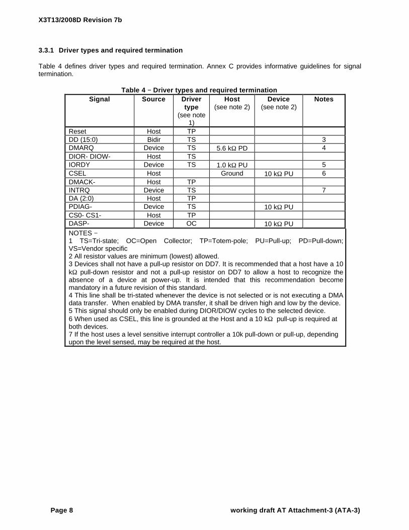
3.3.1 Driver types and required termination
Table 4 defines driver types and required termination. Annex C provides informative guidelines for signaltermination.
Table 4 −− Driver types and required terminationSignal Source Driver
type(see note
1)
Host(see note 2)
Device(see note 2)
Notes
Reset Host TPDD (15:0) Bidir TS 3DMARQ Device TS 5.6 kΩ PD 4DIOR- DIOW- Host TSIORDY Device TS 1.0 kΩ PU 5CSEL Host Ground 10 kΩ PU 6DMACK- Host TPINTRQ Device TS 7DA (2:0) Host TPPDIAG- Device TS 10 kΩ PUCS0- CS1- Host TPDASP- Device OC 10 kΩ PUNOTES −1 TS=Tri-state; OC=Open Collector; TP=Totem-pole; PU=Pull-up; PD=Pull-down;VS=Vendor specific2 All resistor values are minimum (lowest) allowed.3 Devices shall not have a pull-up resistor on DD7. It is recommended that a host have a 10kΩ pull-down resistor and not a pull-up resistor on DD7 to allow a host to recognize theabsence of a device at power-up. It is intended that this recommendation becomemandatory in a future revision of this standard.4 This line shall be tri-stated whenever the device is not selected or is not executing a DMAdata transfer. When enabled by DMA transfer, it shall be driven high and low by the device.5 This signal should only be enabled during DIOR/DIOW cycles to the selected device.6 When used as CSEL, this line is grounded at the Host and a 10 kΩ pull-up is required atboth devices.7 If the host uses a level sensitive interrupt controller a 10k pull-down or pull-up, dependingupon the level sensed, may be required at the host.

X3T13/2008D Revision 7b
working draft AT Attachment-3 (ATA-3) Page 9
4 Interface signal assignments and descriptions
4.1 Signal summary
The physical interface consists of receivers and drivers communicating through a set of conductors using anasynchronous interface protocol. Table 5 defines the signal names. For connector descriptions see annexA.
Table 5 −− Interface signal name assignmentsDescription Host Dir Dev AcronymCable select (see note) CSELChip select 0 → CS0-Chip select 1 → CS1-Data bus bit 0 ↔ DD0Data bus bit 1 ↔ DD1Data bus bit 2 ↔ DD2Data bus bit 3 ↔ DD3Data bus bit 4 ↔ DD4Data bus bit 5 ↔ DD5Data bus bit 6 ↔ DD6Data bus bit 7 ↔ DD7Data bus bit 8 ↔ DD8Data bus bit 9 ↔ DD9Data bus bit 10 ↔ DD10Data bus bit 11 ↔ DD11Data bus bit 12 ↔ DD12Data bus bit 13 ↔ DD13Data bus bit 14 ↔ DD14Data bus bit 15 ↔ DD15Device active or slave (Device 1) present (see note) DASP-Device address bit 0 → DA0Device address bit 1 → DA1Device address bit 2 → DA2DMA acknowledge → DMACK-DMA request ← DMARQInterrupt request ← INTRQI/O read → DIOR-I/O ready ← IORDYI/O write → DIOW-Passed diagnostics (see note) PDIAG-Reset → RESET-NOTE − See signal descriptions for information on source of these signals
4.2 Signal descriptions
4.2.1 CS0- (CHIP SELECT 0)
This is the chip select signal from the host used to select the Command Block registers. Table 6 defines itsuse.

X3T13/2008D Revision 7b
Page 10 working draft AT Attachment-3 (ATA-3)
4.2.2 CS1- (CHIP SELECT 1)
This is the chip select signal from the host used to select the Control Block registers. Table 6 defines its use.
4.2.3 DA2, DA1, and DA0 (DEVICE ADDRESS)
This is the 3-bit binary coded address asserted by the host to access a register or data port in the device.Table 6 defines this address.
4.2.4 DASP- (Device active, device 1 present)
This is a time-multiplexed signal which indicates that a device is active, or that Device 1 is present. Thissignal shall be an open collector output and each device shall have a 10 kΩ pull-up resistor.
If the host connects to the DASP- signal for the illumination of an LED or for any other purpose, the hostshall ensure that the signal level seen on the ATA interface for DASP- shall maintain VoH and VoLcompatibility, given the IoH and IoL requirements of the DASP- device drivers.
4.2.5 DD (15:0) (Device data)
This is an 8- or 16-bit bi-directional data interface between the host and the device. The lower 8 bits areused for 8-bit register transfers.
4.2.6 DIOR- (Device I/O read)
This is the read strobe signal from the host. The falling edge of DIOR- enables data from the device ontothe signals, DD (7:0) or DD (15:0). The rising edge of DIOR- latches data at the host and the host shall notact on the data until it is latched.
4.2.7 DIOW- (Device I/O write)
This is the Write strobe signal from the host. The rising edge of DIOW- latches data from the signals, DD(7:0) or DD (15:0), into the device. The device shall not act on the data until it is latched.
4.2.8 DMACK- (DMA acknowledge)
This signal shall be used by the host in response to DMARQ to initiate DMA transfers.
4.2.9 DMARQ (DMA request)
This signal, used for DMA data transfers between host and device, shall be asserted by the device when it isready to transfer data to or from the host. The direction of data transfer is controlled by DIOR- and DIOW-.This signal is used in a handshake manner with DMACK- i.e., the device shall wait until the host assertsDMACK- before negating DMARQ, and re-asserting DMARQ if there is more data to transfer.
This line shall be released (high impedance state) whenever the device is not selected or is selected and noDMA command is in progress. When enabled by DMA transfer, it shall be driven high and low by the device.
When a DMA operation is enabled, CS0- and CS1- shall not be asserted and transfers shall be 16-bits wide.
4.2.10 INTRQ (Device interrupt)
This signal is used to interrupt the host system. INTRQ is asserted only when the device has a pendinginterrupt, the device is selected, and the host has cleared the nIEN bit in the Device Control register. If thenIEN bit is equal to one, or the device is not selected, this output is in a high impedance state, regardless ofthe presence or absence of a pending interrupt.
X3T13/2008D Revision 7b
working draft AT Attachment-3 (ATA-3) Page 11
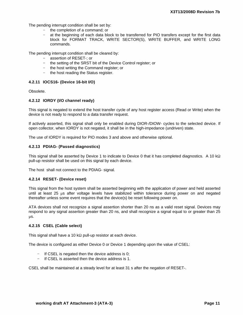
The pending interrupt condition shall be set by:− the completion of a command; or− at the beginning of each data block to be transferred for PIO transfers except for the first data
block for FORMAT TRACK, WRITE SECTOR(S), WRITE BUFFER, and WRITE LONGcommands.
The pending interrupt condition shall be cleared by:− assertion of RESET-; or− the setting of the SRST bit of the Device Control register; or− the host writing the Command register; or− the host reading the Status register.
4.2.11 IOCS16- (Device 16-bit I/O)
Obsolete.
4.2.12 IORDY (I/O channel ready)
This signal is negated to extend the host transfer cycle of any host register access (Read or Write) when thedevice is not ready to respond to a data transfer request.
If actively asserted, this signal shall only be enabled during DIOR-/DIOW- cycles to the selected device. Ifopen collector, when IORDY is not negated, it shall be in the high-impedance (undriven) state.
The use of IORDY is required for PIO modes 3 and above and otherwise optional.
4.2.13 PDIAG- (Passed diagnostics)
This signal shall be asserted by Device 1 to indicate to Device 0 that it has completed diagnostics. A 10 kΩpull-up resistor shall be used on this signal by each device.
The host shall not connect to the PDIAG- signal.
4.2.14 RESET- (Device reset)
This signal from the host system shall be asserted beginning with the application of power and held asserteduntil at least 25 µs after voltage levels have stabilized within tolerance during power on and negatedthereafter unless some event requires that the device(s) be reset following power on.
ATA devices shall not recognize a signal assertion shorter than 20 ns as a valid reset signal. Devices mayrespond to any signal assertion greater than 20 ns, and shall recognize a signal equal to or greater than 25µs.
4.2.15 CSEL (Cable select)
This signal shall have a 10 kΩ pull-up resistor at each device.
The device is configured as either Device 0 or Device 1 depending upon the value of CSEL:
− If CSEL is negated then the device address is 0;− If CSEL is asserted then the device address is 1.
CSEL shall be maintained at a steady level for at least 31 s after the negation of RESET-.

X3T13/2008D Revision 7b
Page 12 working draft AT Attachment-3 (ATA-3)
NOTE − Special cabling can be used by the system manufacturer to selectively groundCSEL e.g., CSEL of Device 0 is connected to the CSEL conductor in the cable, and isgrounded, thus allowing the device to recognize itself as Device 0. CSEL of Device 1 is notconnected to CSEL because the conductor is removed, thus the device can recognize itselfas Device 1. Figure 2 shows possible configurations.
CSEL conductor
Open Ground
Host Device 0 Device 1
CSEL conductor
Open Ground
Host Device 1
CSEL conductor
Open Ground
Host Device 0
Figure 2 −− Cable select example

X3T13/2008D Revision 7b
working draft AT Attachment-3 (ATA-3) Page 13
5 Interface register definitions and descriptions
5.1 Device addressing considerations
In traditional controller operation, only the selected device receives commands from the host followingselection. In this standard, the register contents go to both devices (and their embedded controllers). Thehost discriminates between the two by using the DEV bit in the Device/Head register.
Data is transferred in parallel either to or from host memory to the device's buffer under the direction ofcommands previously transferred from the host. The device performs all of the operations necessary toproperly write data to, or read data from, the media. Data read from the media is stored in the device'sbuffer pending transfer to the host memory and data is transferred from the host memory to the device'sbuffer to be written to the media.
The devices using this interface shall be programmed by the host computer to perform commands andreturn status to the host at command completion. When two devices are daisychained on the interface,commands are written in parallel to both devices, and for all except the EXECUTE DEVICE DIAGNOSTICScommand, only the selected device executes the command. On an EXECUTE DEVICE DIAGNOSTICScommand addressed to Device 0, both devices shall execute the command, and Device 1 shall post itsstatus to Device 0 via PDIAG-.
Devices are selected by the DEV bit in the Device/Head register (see 5.2.8). When the DEV bit is equal tozero, Device 0 is selected. When the DEV bit is equal to one, Device 1 is selected. When devices are daisychained, one shall be set as Device 0 and the other as Device 1.
5.2 I/O register descriptions
Communication to or from the device is through an I/O Register that routes the input or output data to orfrom registers addressed by the signals from the host (CS0-, CS1-, DA (2:0), DIOR-, and DIOW-).
The Command Block Registers are used for sending commands to the device or posting status from thedevice. The Control Block Registers are used for device control and to post alternate status.
Anytime a command is in progress, that is, from the time the Command register is written until the devicehas completed the command and posted ending status, the device shall have either BSY or DRQ set to one.If the Command Block registers are read by the host when BSY or DRQ is set to one, the content of allregister bits and fields except BSY and DRQ in the Status and Alternate Status registers is indeterminant. Ifthe host writes to any Command Block register when BSY or DRQ is set to one, the results areindeterminant and may result in the command in progress ending with a command abort error.
When performing DMA transfers, BSY and DRQ shall both be cleared to zero within 400 ns of INTRQassertion. This signals the completion of a DMA command.
When performing PIO transfers, BSY and DRQ shall both be cleared to zero within 400 ns of the transfer ofthe final byte of data. This assertion signals the completion of a PIO data transfer command.
Table 6 lists these registers and the addresses that select them.

X3T13/2008D Revision 7b
Page 14 working draft AT Attachment-3 (ATA-3)
Table 6 −− I/O port functions and selection addressesAddresses Functions
CS0- CS1- DA2 DA1 DA0 Read (DIOR-) Write (DIOW-)N N x x x Data bus high impedence Not used
Control block registersN A 0 x x Data bus high impedence Not usedN A 1 0 x Data bus high impedence Not usedN A 1 1 0 Alternate Status Device ControlN A 1 1 1 (see note 1) Not used
Command block registersA N 0 0 0 Data DataA N 0 0 1 Error FeaturesA N 0 1 0 Sector Count Sector CountA N 0 1 1 Sector Number
LBA (7:0) (see note 2)Sector Number
LBA (7:0) (see note 2)A N 1 0 0 Cylinder Low
LBA (15:8) (see note 2)Cylinder Low
LBA (15:8) (see note 2)A N 1 0 1 Cylinder High
LBA (23:16) (see note 2)Cylinder High
LBA (23:16) (see note 2)A N 1 1 0 Device/Head
LBA (27:24) (see note 2)Device/Head
LBA (27:24)(see note 2)A N 1 1 1 Status CommandA A x x x Invalid address Invalid address
Key:A = signal asserted, N = signal negated, x = don’t careNOTES −1 This register is obsolete. It is recommended that a device not respond to a read of this address. Ifa device does respond, it shall not drive the DD7 signal to prevent possible conflict with floppy diskimplementations.2 Mapping of registers in LBA translation.
Each register description in the following clauses contain the following format:
ADDRESS - the CS and DA address of the register.
DIRECTION - indicates if the register is read/write, read only, or write only from the host.
ACCESS RESTRICTIONS - indicates when the register may be accessed.
EFFECT - indicates the effect of accessing the register.
FUNCTIONAL DESCRIPTION - describes the function of the register.
FIELD/BIT DESCRIPTION - describes the content of the register.
X3T13/2008D Revision 7b
working draft AT Attachment-3 (ATA-3) Page 15
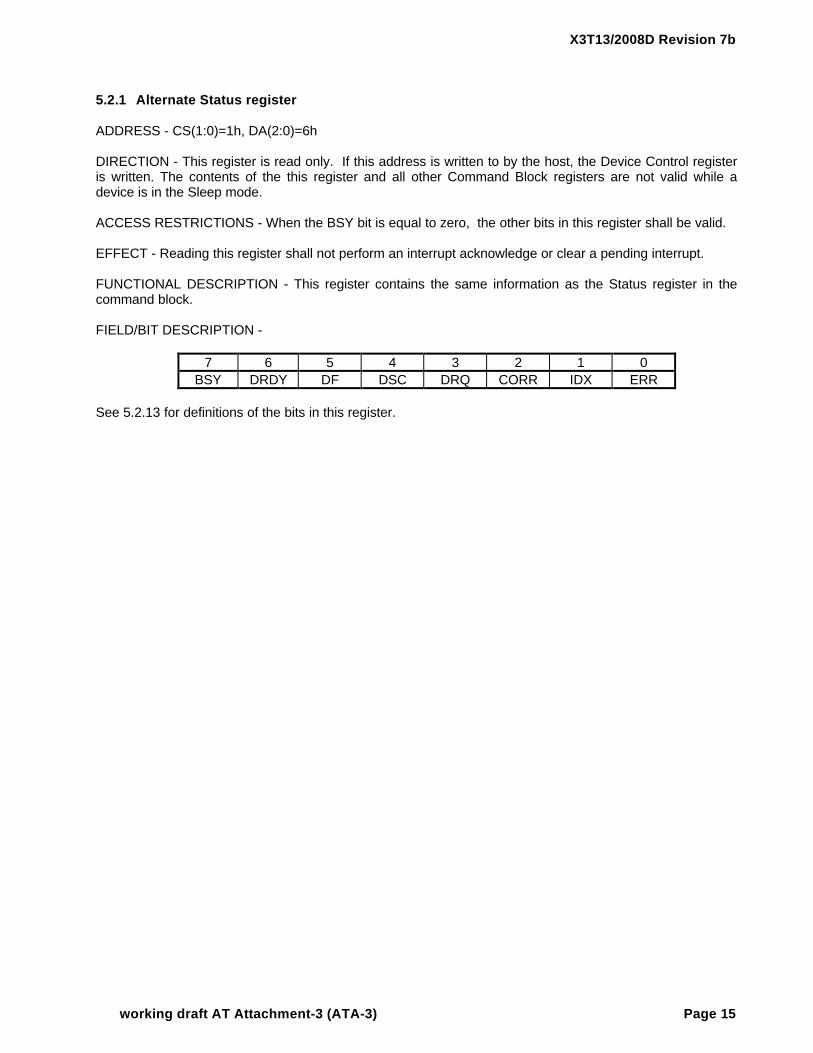
5.2.1 Alternate Status register
ADDRESS - CS(1:0)=1h, DA(2:0)=6h
DIRECTION - This register is read only. If this address is written to by the host, the Device Control registeris written. The contents of the this register and all other Command Block registers are not valid while adevice is in the Sleep mode.
ACCESS RESTRICTIONS - When the BSY bit is equal to zero, the other bits in this register shall be valid.
EFFECT - Reading this register shall not perform an interrupt acknowledge or clear a pending interrupt.
FUNCTIONAL DESCRIPTION - This register contains the same information as the Status register in thecommand block.
FIELD/BIT DESCRIPTION -
7 6 5 4 3 2 1 0BSY DRDY DF DSC DRQ CORR IDX ERR
See 5.2.13 for definitions of the bits in this register.

X3T13/2008D Revision 7b
Page 16 working draft AT Attachment-3 (ATA-3)
5.2.2 Command register
ADDRESS - CS(1:0)=2h, DA(2:0)=7h
DIRECTION - This register is write-only. If this address is read by the host, the Status register is read.
ACCESS RESTRICTIONS - This register shall only be written when BSY and DRQ are both equal to zeroand DMACK- is not asserted. The contents of the this register and all other Command Block registers arenot valid while a device is in the Sleep mode.
EFFECT - Command processing begins when this register is written. The content of the Command Blockregisters become parameters of the command when this register is written. Writing this register clears anypending interrupt condition.
FUNCTIONAL DESCRIPTION - This register contains the command code being sent to the device.Command execution begins immediately after this register is written. The executable commands, thecommand codes, and the necessary parameters for each command are listed in clause 7.
FIELD/BIT DESCRIPTION -
7 6 5 4 3 2 1 0Command Code

X3T13/2008D Revision 7b
working draft AT Attachment-3 (ATA-3) Page 17
5.2.3 Cylinder High register
ADDRESS - CS(1:0)=2h, DA(2:0)=5h
DIRECTION - This register is read/write.
ACCESS RESTRICTIONS - This register shall be written only when both BSY and DRQ are zero andDMACK- is not asserted. The contents of this register are valid only when both BSY and DRQ are zero. Ifthis register is written when BSY or DRQ is set to one, the result is indeterminant. The contents of the thisregister and all other Command Block registers are not valid while a device is in the Sleep mode.
EFFECT - Information written to this register becomes a command parameter when subsequentcommands are written to the Command register.
FUNCTIONAL DESCRIPTION - If the LBA bit is cleared to zero in the Device/Head register, this registercontains the high order bits of the starting cylinder address for any media access. If the LBA bit is set to onein the Device/Head register, this register contains Bits 23-16 of the LBA for any media access.
This register shall be updated to reflect the address of the first error when a media access command isunsuccessfully completed.
FIELD/BIT DESCRIPTION -
CHS
7 6 5 4 3 2 1 0Cylinder(15:8)
LBA
7 6 5 4 3 2 1 0LBA(23:16)
X3T13/2008D Revision 7b
Page 18 working draft AT Attachment-3 (ATA-3)
5.2.4 Cylinder Low register
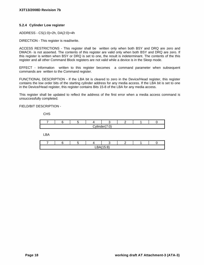
ADDRESS - CS(1:0)=2h, DA(2:0)=4h
DIRECTION - This register is read/write.
ACCESS RESTRICTIONS - This register shall be written only when both BSY and DRQ are zero andDMACK- is not asserted. The contents of this register are valid only when both BSY and DRQ are zero. Ifthis register is written when BSY or DRQ is set to one, the result is indeterminant. The contents of the thisregister and all other Command Block registers are not valid while a device is in the Sleep mode.
EFFECT - Information written to this register becomes a command parameter when subsequentcommands are written to the Command register.
FUNCTIONAL DESCRIPTION - If the LBA bit is cleared to zero in the Device/Head register, this registercontains the low order bits of the starting cylinder address for any media access. If the LBA bit is set to onein the Device/Head register, this register contains Bits 15-8 of the LBA for any media access.
This register shall be updated to reflect the address of the first error when a media access command isunsuccessfully completed.
FIELD/BIT DESCRIPTION -
CHS
7 6 5 4 3 2 1 0Cylinder(7:0)
LBA
7 6 5 4 3 2 1 0LBA(15:8)

X3T13/2008D Revision 7b
working draft AT Attachment-3 (ATA-3) Page 19
5.2.5 Data register
ADDRESS - CS(1:0)=2h, DA(2:0)=0h
DIRECTION - This register is read/write.
ACCESS RESTRICTIONS - This register shall be written and the contents shall be valid on read only whenDRQ is set to one and DMACK- is not asserted. The contents of the this register and all other CommandBlock registers are not valid while a device is in the Sleep mode.
EFFECT - PIO out data transfers are processed by a series of reads to this register, each read transferringthe data that follows the previous read. PIO in data transfers are processed by a series of writes to thisregister, each write transferring the data that follows the previous write. The results of a read during a PIO inor a write during a PIO out are indeterminant.
FUNCTIONAL DESCRIPTION - The data register is 16-bits wide.
FIELD/BIT DESCRIPTION -
15 14 13 12 11 10 9 8Data(15:8)
7 6 5 4 3 2 1 0Data(7:0)

X3T13/2008D Revision 7b
Page 20 working draft AT Attachment-3 (ATA-3)
5.2.6 Data port
ADDRESS - None.
DIRECTION - This port is read/write.
ACCESS RESTRICTIONS - This port shall be written and the contents shall be valid on read only whenDMACK- is asserted.
EFFECT - DMA out data transfers are processed by a series of reads to this port, each read transferring thedata that follows the previous read. DMA in data transfers are processed by a series of writes to this register,each write transferring the data that follows the previous write. The results of a read during a DMA in or awrite during a DMA out are indeterminant.
FUNCTIONAL DESCRIPTION - The data port is 16-bits in width.
FIELD/BIT DESCRIPTION -
15 14 13 12 11 10 9 8Data(15:8)
7 6 5 4 3 2 1 0Data(7:0)

X3T13/2008D Revision 7b
working draft AT Attachment-3 (ATA-3) Page 21
5.2.7 Device Control register
ADDRESS - CS(1:0)=1h, DA(2:0)=6h
DIRECTION - This register is write only. If this address is read by the host, the Alternate Status register isread.
ACCESS RESTRICTIONS - This register shall only be written when DMACK- is not asserted.
EFFECTIVENESS - the content of this register shall take effect when written.
FUNCTIONAL DESCRIPTION - This register allows a host to software reset attached devices andenable/disable interrupts.
FIELD/BIT DESCRIPTION -
7 6 5 4 3 2 1 0r r r r r SRST nIEN 0
− Bits 7 through 3 are reserved;− SRST is the host software reset bit (see 8.2);− nIEN is the enable bit for the device interrupt to the host. When the nIEN bit is equal to zero, and
the device is selected, INTRQ shall be enabled through a tri-state buffer. When the nIEN bit is equalto one, or the device is not selected, the INTRQ signal shall be in a high impedance state;
− Bit 0 shall be written with zero.

X3T13/2008D Revision 7b
Page 22 working draft AT Attachment-3 (ATA-3)
5.2.8 Device/Head register
ADDRESS - CS(1:0)=2h, DA(2:0)=6h
DIRECTION - This register is read/write.
ACCESS RESTRICTIONS - This register shall be written only when both BSY and DRQ are zero andDMACK- is not asserted. The contents of this register are valid only when BSY and DRQ equal zero. If thisregister is written when BSY or DRQ is set to one, the result is indeterminant. The contents of the thisregister and all other Command Block registers are not valid while a device is in the Sleep mode.
EFFECT - The DRV bit becomes becomes effective when this register is written. All other bits in this registerbecome a command parameter when subsequent commands are written to the Command register.
FUNCTIONAL DESCRIPTION - This register selects the device, defines address translation as CHS orLBA, and provides the head address if CHS or LBA (27:24) if LBA.
FIELD/BIT DESCRIPTION -
CHS
7 6 5 4 3 2 1 01 LBA 1 DEV HS3 HS2 HS1 HS0
LBA
7 6 5 4 3 2 1 01 LBA 1 DEV LBA(27:24)
− Bit 7 shall be set to one for backward compatibility;
NOTE − This bit may be reclaimed for use in a future ATA standard.
− LBA. When this bit is equal to zero, addressing is by CHS. When this bit is equal to one,addressing is by LBA;
− Bit 5 shall be set to one for backward compatibility;
NOTE − This bit may be reclaimed for use in a future ATA standard.
− DEV is the device address. When the DEV bit is equal to zero, Device 0 is selected. When theDEV bit is equal to one, Device 1 is selected;
− Bit 3-0 If LBA is equal to zero (CHS), these contain the head address of the starting CHS address.The HS3 bit is the most significant bit. If LBA is equal to one (LBA), these bits contain bits 27through 24 of the LBA. This field shall be updated to reflect the media address of the error when amedia access command is unsuccessfully completed (see 6.2).

X3T13/2008D Revision 7b
working draft AT Attachment-3 (ATA-3) Page 23
5.2.9 Error register
ADDRESS - CS(1:0)=2h, DA(2:0)=1h
DIRECTION - This register is read only. If this address is written to, the Features register is written.
ACCESS RESTRICTIONS - The contents of this register shall be valid when BSY and DRQ equal zero andERR equals one. The contents of this register shall be valid upon completion of power on or a reset. Thecontents of this register shall be valid at the completion of an EXECUTE DEVICE DIAGNOSTIC command.The contents of the this register and all other Command Block registers are not valid while a device is in theSleep mode.
EFFECT - None.
FUNCTIONAL DESCRIPTION - This register contains status for the current command.
Following a power on, a reset, or completion of an EXECUTE DEVICE DIAGNOSTIC command, thisregister contains a diagnostic code (see 7.5).
At the completion of any command except EXECUTE DEVICE DIAGNOSTIC, the contents of this registerare valid when the ERR bit is equal to one in the Status register.
FIELD/BIT DESCRIPTION -
7 6 5 4 3 2 1 0r UNC MC IDNF MCR ABRT TK0NF AMNF
− Bit 7 is reserved;− UNC (Uncorrectable Data Error) indicates an uncorrectable data error has been encountered;− MC (Media Changed) is used by removable media devices and indicates that new media is
available to the operating system (see 6.4);− IDNF (ID Not Found) indicates the requested sector's ID field could not be found;− MCR (Media Change Requested) is used by removable media devices and indicates that a
request for media removal has been detected by the device (see 6.4);− ABRT (Aborted Command) indicates the requested command has been aborted because the
command code or a command parameter is invalid or some other error has occurred. Thedevice may complete some portion of the command prior to setting ABRT and terminating thecommand. If the command was a data transfer command, the data transferred is indeterminant;
− TK0NF (Track 0 Not Found) indicates track 0 has not been found during a RECALIBRATEcommand;
− AMNF (Address Mark Not Found) indicates the data address mark has not been found afterfinding the correct ID field.

X3T13/2008D Revision 7b
Page 24 working draft AT Attachment-3 (ATA-3)
5.2.10 Features register
ADDRESS - CS(1:0)=2h, DA(2:0)=1h
DIRECTION - This register is write only. If this address is read by the host, the Error register is read.
ACCESS RESTRICTIONS - This register shall be written only when BSY and DRQ equal zero and DMACK-is not asserted. If this register is written when BSY or DRQ is set to one, the result is indeterminant.
EFFECT - Information written to this register becomes a command parameter when subsequentcommands are written to the Command register.
FUNCTIONAL DESCRIPTION - This register is command specific.
FIELD/BIT DESCRIPTION -
7 6 5 4 3 2 1 0Command specific

X3T13/2008D Revision 7b
working draft AT Attachment-3 (ATA-3) Page 25
5.2.11 Sector Count register
ADDRESS - CS(1:0)=2h, DA(2:0)=2h
DIRECTION - This register is read/write.
ACCESS RESTRICTIONS - This register shall be written only when both BSY and DRQ are zero andDMACK- is not asserted. The contents of this register are valid only when both BSY and DRQ are zero. Ifthis register is written when BSY or DRQ is set to one, the result is indeterminant. The contents of the thisregister and all other Command Block registers are not valid while a device is in the Sleep mode.
EFFECT - Information written to this register becomes a command parameter when subsequentcommands are written to the Command register.
FUNCTIONAL DESCRIPTION - This register contains the number of sectors of data requested to betransferred on a read or write operation between the host and the device. If the value in this register is zero,a count of 256 sectors is specified.
For media access commands that complete with an error indication in the Status register, this registercontains the number of sectors which need to be transferred in order to complete the request.
The contents of this register may be redefined on some commands.
FIELD/BIT DESCRIPTION -
7 6 5 4 3 2 1 0Sector Count

X3T13/2008D Revision 7b
Page 26 working draft AT Attachment-3 (ATA-3)
5.2.12 Sector Number register
ADDRESS - CS(1:0)=2h, DA(2:0)=3h
DIRECTION - This register is read/write.
ACCESS RESTRICTIONS - This register shall be written only when both BSY and DRQ are zero andDMACK- is not asserted. The contents of this register are valid only when both BSY and DRQ are zero. Ifthis register is written when BSY or DRQ is set to one, the result is indeterminant. The contents of the thisregister and all other Command Block registers are not valid while a device is in the Sleep mode.
EFFECT - Information written to this register becomes a command parameter when subsequent commandsare written to the Command register.
FUNCTIONAL DESCRIPTION - If the LBA bit is cleared to zero in the Device/Head register, this registercontains the starting sector number for any media access. If the LBA bit is set to one in the Device/Headregister, this register contains Bits 7-0 of the LBA for any media access. This register is used by some non-media access commands to pass command specific information from the host to the device, or from thedevice to the host.
This register shall be updated to reflect the media address of the error when a media access command isunsuccessfully completed.
FIELD/BIT DESCRIPTION -
CHS
7 6 5 4 3 2 1 0Sector(7:0)
LBA
7 6 5 4 3 2 1 0LBA(7:0)

X3T13/2008D Revision 7b
working draft AT Attachment-3 (ATA-3) Page 27
5.2.13 Status register
ADDRESS - CS(1:0)=2h, DA(2:0)=7h
DIRECTION - This register is read only. If this address is written to by the host, the Command register iswritten.
ACCESS RESTRICTIONS - The contents of this register, except for BSY, shall be ignored when BSY is setequal to one. BSY is valid at all times. The contents of the this register and all other Command Blockregisters are not valid while a device is in the Sleep mode.
EFFECT - Reading this register when an interrupt is pending causes the interrupt to be cleared (see 4.2.10).
FUNCTIONAL DESCRIPTION - This register contains the device status. The contents of this register areupdated to reflect the current state of the device and the progress of any command being executed by thedevice. When the BSY bit is equal to zero, the other bits in this register are valid. When the BSY bit is equalto one, other bits in this register are not valid.
NOTE − Although host systems might be capable of generating read cycles shorter than the400 ns specified for status update following the last command or data cycle, hostimplementations should wait at least 400 ns before reading the Status register to insure thatthe BSY bit is valid.
FIELD/BIT DESCRIPTION -
7 6 5 4 3 2 1 0BSY DRDY DF DSC DRQ CORR IDX ERR
− BSY (Busy) is set whenever the device has control of the command Block Registers. When theBSY bit is equal to one, a write to a command block register by the host shall be ignored by thedevice.
The device shall not change the state of the DRQ bit unless the BSY bit is equal to one. When thelast block of a PIO data in command has been transferred by the host, then the DRQ bit is clearedwithout the BSY bit being set.
When the BSY bit equals zero, the device may only change the IDX, DRDY, DF, DSC, and CORRbits in the Status register and the Data register. None of the other command block registers norother bits within the Status register shall be changed by the device.
NOTE − BIOSs and software device drivers that sample status as soon as the BSYbit is cleared to zero may not detect the assertion of the CORR bit by the device.
After the host has written the Command register either the BSY bit shall be set, or if the BSY bit iscleared, the DRQ bit shall be set, until command completion.
NOTE − The BSY bit is set and then cleared so quickly, that host detection of theBSY bit being set is not certain.
The BSY bit shall be set by the device under the following circumstances:
a) within 400 ns after either the negation of RESET- or the setting of the SRST bit in theDevice Control register;

X3T13/2008D Revision 7b
Page 28 working draft AT Attachment-3 (ATA-3)
b) within 400 ns after writing the Command register if the DRQ bit is not set;
c) between blocks of a data transfer during PIO data in commands if the DRQ bit is not set;
d) after the transfer of a data block during PIO data out commands if the DRQ bit is not set;
e) during the data transfer of DMA commands if the DRQ bit is not set.
The device shall not set the BSY bit at any other time.
− DRDY (Device Ready) is set to indicate that the device is capable of accepting all command codes.This bit shall be cleared at power on. Devices that implement the power management features shallmaintain the DRDY bit equal to one when they are in the Idle or Standby power modes. When thestate of the DRDY bit changes, it shall not change again until after the host reads the Statusregister.
When the DRDY bit is equal to zero, a device responds as follows:
a) the device shall accept and attempt to execute the EXECUTE DEVICE DIAGNOSTICand INITIALIZE DEVICE PARAMETERS commands;
b) If a device accepts commands other than EXECUTE DEVICE DIAGNOSTIC andINITIALIZE DEVICE PARAMETERS during the time the DRDY bit is equal to zero, theresults are vendor specific.
− DF (Device Fault) indicates a device fault error has been detected. The internal status or internalconditions that causes this error to be indicated is vendor specific.
− DSC (Device Seek Complete) indicates that the device heads are settled over a track. When anerror occurs, this bit shall not be changed until the Status register is read by the host, at which timethe bit again indicates the current Seek Complete status.
− DRQ (Data Request) indicates that the device is ready to transfer a word or byte of data betweenthe host and the device.
− CORR (Corrected Data) is used to indicate a correctable data error. The definition of whatconstitutes a correctable error is vendor specific. This condition does not terminate a data transfer.
− IDX (Index) is vendor specific.
− ERR (Error) indicates that an error occurred during execution of the previous command. The bits inthe Error register have additional information regarding the cause of the error. Once the device hasset the error bit, the device shall not change the contents of the following items until a new commandhas been accepted, the SRST bit is set to one, or RESET- is asserted:
the ERR bit in the Status registerError registerCylinder High registerCylinder Low registerSector Count registerSector Number registerDevice/Head register.

X3T13/2008D Revision 7b
working draft AT Attachment-3 (ATA-3) Page 29
6 General operational requirements
6.1 Reset response
There are three types of reset in ATA. The following is a suggested method of classifying reset actions:
− Power On Reset: the device executes a series of electrical circuitry diagnostics, spins up theHDA, tests speed and other mechanical parametrics, and sets default values (see 8.1);
− Hardware Reset: the device executes a series of electrical circuitry diagnostics, and resets todefault values (see 8.1);
− Software Reset: the device resets the interface circuitry (see 8.2).
6.2 Sector addressing
All addressing of data sectors recorded on the device's media is by a logical sector address. The mappingof logical sector addresses to the actual physical location of the data sector on the media is vendor specific.
A device shall support at least one logical CHS translation known as the default translation if the devicecapacity is less than or equal to 16,515,072 sectors. The device shall enter this translation following apower-on reset. A device shall support LBA translation regardless of capacity. If the device capacity is equalto or greater than 16,515,072 sectors, the LBA translation shall be the default translation and the deviceshall enter this translation following a power-on reset. A device may support other logical translations if thedevice capacity is less than or equal to 16,515,072 sectors and the host may use the INITIALIZE DEVICEPARAMETERS command to select the translation. The default translation is described in the IDENTIFYDEVICE information. The current translation may also be described in the Identify Device information.
A CHS address is made up of three fields: the sector address, the head number and the cylinder number.Sectors are numbered from 1 to the maximum value allowed by the current CHS translation but can notexceed 255. Heads are numbered from 0 to the maximum value allowed by the current CHS translation butcan not exceed 15. Cylinders are numbered from 0 to the maximum value allowed by the current CHStranslation but cannot exceed 65,535.
When the host selects a CHS translation using the INITIALIZE DEVICE PARAMETERS command, the hostrequests the number of sectors per logical track and the number of heads per logical cylinder. The devicethen computes the number of logical cylinders available in requested translation.
Sequential access to logical sectors shall be accomplished by treating the sector number as the leastsignificant portion of the logical sector address, the head number as the middle portion of the logical sectoraddress, and the cylinder number as the most significant portion of the logical sector address.
A device shall not change the addressing method and shall return status information utilizing the addressingmethod specified for the command.
The following LBA addressing methods shall be supported by the device:
a) The host may select either the currently selected CHS translation addressing or LBA addressing ona command-by-command basis by using the LBA bit in the Device/Head register;
b) The device shall support LBA addressing for all media access commands, except for the FORMATTRACK command. Implementation of LBA addressing for the FORMAT TRACK command isvendor specific. The LBA bit of the Device/Head register shall be ignored for commands that do notaccess the media;
c) Logical sectors on the device shall be linearly mapped with the first LBA addressed sector (sector 0)being the same sector as the first logical CHS addressed sector (cylinder 0, head 0, sector 1).Irrespective of the logical CHS translation currently in effect, the LBA address of a given logicalsector does not change. The following is always true:

X3T13/2008D Revision 7b
Page 30 working draft AT Attachment-3 (ATA-3)
LBA = ( (cylinder * heads_per_cylinder + heads ) * sectors_per_track ) + sector - 1
where heads_per_cylinder and sectors_per_track are the current translation values.
Annex B provides informative information for the implementation of devices with capacity below 8GB.
6.3 Power management feature set
The optional Power Management Feature Set permits a host to modify the behavior of a device in a mannerwhich reduces the power required to operate. The Power Management Feature Set provides a set ofcommands and a timer that enable a device to implement low power consumption modes. A device thatimplements the Power Management feature shall implement the following minimum set of functions:
a) A Standby timer;b) IDLE command;c) IDLE IMMEDIATE command;d) SLEEP command;e) STANDBY command;f) STANDBY IMMEDIATE command.
Additional vendor specific commands and functions are allowed.
6.3.1 Power modes
In Active mode the device is capable of responding to commands. During the execution of a media accesscommand a device shall be in Active mode. Power consumption is greatest in this mode.
In Idle mode the device is capable of responding to commands but the device may take longer to completecommands than when in the Active mode. Power consumption may be reduced from that of Active mode.
In Standby mode the device is capable of responding to commands but the device may take longer tocomplete commands than in the Idle mode. The time to respond could be as long as 30 s. Powerconsumption may be reduced from that of Idle mode.
In Sleep mode the device requires a reset to be activated. The time to respond could be as long as 30 s.Sleep provides the lowest power consumption of any mode.
6.3.2 Power management commands
The CHECK POWER MODE command allows a host to determine if a device is currently in, going to, orleaving Standby or Idle mode.
The IDLE and IDLE IMMEDIATE commands move a device to Idle mode immediately from the Active orStandby modes. The Idle command also sets the Standby Timer count and enables or disables the StandbyTimer.
The SLEEP command moves a device to Sleep mode. The device's interface becomes inactive at thecompletion of the SLEEP command. A reset is required to move a device out of Sleep mode. When adevice exits Sleep mode it may enter Active, Idle or Standby mode. The mode selected by the device isbased on the type of reset received and on vendor specific implementation.
The STANDBY and STANDBY IMMEDIATE commands move a device to Standby mode immediately fromthe Active or Idle modes. The STANDBY command also sets the Standby Timer count and enables ordisables the Standby Timer.

X3T13/2008D Revision 7b
working draft AT Attachment-3 (ATA-3) Page 31
6.3.3 Standby timer
The Standby timer provides a method for the device to automatically enter Standby mode from either Activeor Idle mode following a host programmed period of inactivity. If the Standby timer is enabled and if thedevice is in the Active or Idle mode, the device waits for the specified time period and if no command isreceived, the device automatically enters the Standby mode.
If the Standby Timer is disabled, the device may not automatically enter Standby mode.
6.3.4 Idle mode transition
The transition to Idle mode is vendor specific, and may occur as a result of an IDLE or IDLE IMMEDIATEcommand, or in a vendor specific way.
6.3.5 Status
In Sleep mode, the device's interface is not active. The content of the Status register is invalid in this mode.
6.3.6 Power mode transitions
Figure 3 shows the minimum set of mode transitions that shall be implemented.
1 Active 3 4 4 5 2 Idle Standby 3
5 Sleep 5
Resets 6 6
(see path 6)
Path 1: An IDLE command, IDLE IMMEDIATE command, or vendor specific implementation moves the device to Idle mode. Path 2: An IDLE command or IDLE IMMEDIATE command moves the device to Idle mode. Path 3: A STANDBY command, STANDBY IMMEDIATE command, vendor specific implementation, or Standby timer expiration moves the device to Standby mode. Path 4: A Media access command moves the device to Active mode. Path 5: A SLEEP command moves the device to Sleep mode. Path 6: A reset, either hardware or software, moves the device to Active, Idle or Standby as specified by the device vendor.
Figure 3 −− Power management modes

X3T13/2008D Revision 7b
Page 32 working draft AT Attachment-3 (ATA-3)
6.4 Removable media mode transitions
Figure 4 shows the minimum set of mode transitions that shall be implemented by removable media deviceswhich contain a media change request mechanism (button) and support the DOOR LOCK and DOORUNLOCK commands, and the MC and MCR bits in the Error register.
State A Ready Unlocked Door closed Button off MC active
1. Any command MC status
10.Door State B State C closed Ready 3. Door lock Ready 5.Door lock and Unlocked Locked button Door closed Door closed off Button off 4. Door unlock Button off Good MC cleared status
2. Media change 6. Media change Request Request (Button pushed) (Button pushed)
State E 8. Door unlock State D Not ready Ready 7. Door lock Unlocked 9. Door lock Locked Door open Door closed MCR status ABRT status Button pushed State A: Following a media change, the device is ready, the media is not locked, the door is closed, the media change
request button is not active and a media change has been detected.Path 1: The first command following a media change shall be rejected with the MC bit set in the Error register
and the ERR bit set in the Status register. The device shall then be moved to state B, the MCcondition cleared and susequent commands accepted normally.
State B: In normal operation, the device is ready, the media is not locked, the door is closed, the media changerequest button is not active and the MC bit is off.
Path 2: Activating the media change request button shall cause the device to complete any pendingoperations, spin down the device, if needed, and move to state E, allowing media removal.
Path 3: A DOOR LOCK command shall lock the media and move the device to state C. State C: In normal operation, the device is ready, the media is locked, the door is closed and the media change
request button is not active.Path 4: A DOOR UNLOCK command shall unlock the media and move the device to state B.Path 5: A DOOR LOCK command shall return good status.Path 6: Pushing the media change button shall move the device to state D.
State D: The device is ready, the media is locked, the door is closed and the media change button is active.Path 7: A DOOR LOCK command shall return MCR status in the Error register and the ERR bit in the Status register. The device shall remain in state D..Path 8: A DOOR UNLOCK command or a hard reset shall move the device to state E, allowing media
removal. State E: The device is not ready, the media is not locked and the door is open.
Path 9: A DOOR LOCK command shall return an ABRT error status.Path 10: If the door is closed and the Media Change Button is inactive, the device shall move the device to
state A (ready) and shall set the MC bit.Note: A MEDIA EJECT command, while in states B, C, or D, will unlock the door or media , iflocked, and cause the device to transition to state E (see 7.12).
Figure 4 −− Removable modes

X3T13/2008D Revision 7b
working draft AT Attachment-3 (ATA-3) Page 33
6.5 Security mode feature set
The Security mode features allow a host to implement a security password system to prevent unauthorizedaccess to the internal disk drive.
The Commands supported by this feature set are:
− SECURITY SET PASSWORD− SECURITY UNLOCK− SECURITY ERASE PREPARE− SECURITY ERASE UNIT− SECURITY FREEZE LOCK− SECURITY DISABLE PASSWORD
Support of the Security mode feature set is indicated in IDENTIFY DEVICE response Word 128.
6.5.1 Security mode default setting
The Master Password shall be set to a vendor specific value during manufactuing and the lock functiondisabled.
The system manufacturer/dealer may set a new Master Password using the SECURITY SET PASSWORDcommand, without enabling or disabling the lock function.
6.5.2 Initial setting of the user password
When a user password is set, the device shall automatically enter lock mode the next time the device ispowered-on or hardware reset.
6.5.3 Security mode operation from power-on or hardware reset
When lock is enabled, the device rejects media access commands until a SECURITY UNLOCK command issuccessfully completed. Figure 5 describes this behavior. Table 7 defines executable commands in eachlock mode state.
6.5.4 User password lost
If the user password is lost and High level security is set, the device shall not allow the user to access data.The device shall be unlocked using the master password. Figure 6 describes this behavior.
If the user password is lost and Maximum security level is set, data access shall be impossible. However,the device shall be unlocked using the SECURITY ERASE UNIT command with the master password tounlock the device and shall erase all user data.
6.5.5 Attempt limit for SECURITY UNLOCK command
The SECURITY UNLOCK command has an attempt limit counter. The purpose of this counter is to defeatrepeated trial attacks. After each failed user or master password SECURITY UNLOCK command, thecounter is decremented. When the counter value reaches zero the EXPIRE bit (bit 4) of word 128 in theIDENTIFY DEVICE information is set, and the SECURITY UNLOCK and SECURITY UNIT ERASEcommands are aborted until the device is powered off or hardware reset. The EXPIRE bit is cleared afterpower on or hardware reset. The counter is reset to five after a power on or hardware reset.

X3T13/2008D Revision 7b
Page 34 working draft AT Attachment-3 (ATA-3)
Power-on
Locked mode
UNLOCK ERASE Media access Non-media PREPARE (see table 7) access (see table 7) No Password ERASE Reject match? UNIT Command Execute Command Yes Unit erased Unlock mode Lock function disabled
Normal operation, all commands are available
FREEZE LOCK
Normal operation, Frozen mode commands are available (see table 7)
Figure 5 −− Password set security mode power-on flow
User password lost
High Level? UNLOCK with master password
Maximum
ERASE PREPARE Normal operation
ERASE UNIT with master password
Normal operation but data lost
Figure 6 −− User password lost

X3T13/2008D Revision 7b
working draft AT Attachment-3 (ATA-3) Page 35
Table 7 −− Security mode command actionsCommand Locked mode Unlocked mode Frozen mode
CHECK POWER MODE Executable Executable ExecutableDOOR LOCK Executable Executable Executable
DOOR UNLOCK Executable Executable ExecutableDOWNLOAD MICROCODE Executable Executable Executable
EXECUTE DEVICE DIAGNOSTICS Executable Executable ExecutableFORMAT TRACK Aborted Executable Executable
IDENTIFY DEVICE Executable Executable ExecutableIDENTIFY DEVICE DMA Executable Executable Executable
IDLE Executable Executable ExecutableIDLE IMMEDIATE Executable Executable Executable
INITIALIZE DEVICE PARAMETERS Executable Executable ExecutableMEDIA EJECT Executable Executable Executable
NOP Executable Executable ExecutableREAD BUFFER Executable Executable Executable
READ DMA Aborted Executable ExecutableREAD LONG Aborted Executable Executable
READ MULTIPLE Aborted Executable ExecutableREAD SECTORS Aborted Executable Executable
READ VERIFY SECTORS Aborted Executable ExecutableRECALIBRATE Executable Executable Executable
SECURITY DISABLE PASSWORD Aborted Executable AbortedSECURITY ERASE PREPARE Executable Executable Executable
SECURITY ERASE UNIT Executable Executable AbortedSECURITY FREEZE LOCK Aborted Executable Executable
SECURITY SET PASSWORD Aborted Executable AbortedSECURITY UNLOCK Executable Executable Aborted
SEEK Executable Executable ExecutableSET FEATURES Executable Executable Executable
SET MULTIPLE MODE Executable Executable ExecutableSLEEP Executable Executable Executable
SMART DISABLE OPERATIONS Executable Executable ExecutableSMART ENABLE/DISABLE AUTOSAVE Executable Executable Executable
SMART ENABLE OPERATIONS Executable Executable ExecutableSMART READ THRESHOLDS Executable Executable Executable
SMART READ VALUES Executable Executable ExecutableSMART RETURN STATUS Executable Executable Executable
SMART SAVE VALUES Executable Executable ExecutableSTANDBY Executable Executable Executable
STANDBY IMMEDIATE Executable Executable ExecutableWRITE BUFFER Executable Executable Executable
WRITE DMA Aborted Executable ExecutableWRITE LONG Aborted Executable Executable
WRITE MULTIPLE Aborted Executable ExecutableWRITE SECTORS Aborted Executable Executable
WRITE VERIFY Aborted Executable Executable

X3T13/2008D Revision 7b
Page 36 working draft AT Attachment-3 (ATA-3)
6.6 Self-monitoring, analysis, and reporting technology
The intent of self-monitoring, analysis, and reporting technology (SMART) is to protect user data andminimize the liklihood of unscheduled system downtime that may be caused by predictable degradationand/or fault of the device. By monitoring and storing critical performance and calibration parameters, SMARTdevices attempt to predict the likelihood of near-term degradation or fault condition. Providing the hostsystem the knowledge of a negative reliability condition, allows the host system to warn the user of theimpending risk of a data loss and advise the user of appropriate action. Support of this feature set isindicated in bit 0 of word 82 of the IDENTIFY DEVICE response.
6.6.1 Attributes
Attributes are the specific performance or calibration parameters that are used in analyzing the status of thedevice. Attributes are selected by the device manufacturer based on that attribute’s ability to contribute tothe prediction of degrading or fault conditions for that particular device. The specific set of attributes beingused and the identity of these attributes is vendor specific and proprietary.
6.6.2 Attribute values
Attribute values are used to represent the relative reliability of individual performance or calibration attributes.The valid range of attribute values is from 1 to 253. Higher attribute values indicate that the analysisalgorithms being used by the device are predicting a lower probability of a degrading or fault conditionexisiting. Accordingly, lower attribute values indicate that the analysis algorithms being used by the deviceare predicting a higher probability of a degrading or fault condition existing.
6.6.3 Attribute thresholds
Each attribute value has a corresponding attribute threshold limit which is used for direct comparison to theattribute value to indicate the existence of a degrading or fault condition. The numerical value of the attributethresholds are determined by the device manufacturer through design and reliability testing and analysis.Each attribute threshold represents the lowest limit to which its corresponding attribute value can be equalwhile still retaining a positive reliability status. Attribute thresholds are set at the device manufacturer’sfactory and cannot be changed in the field. The valid range for attribute thresholds is from 1 through 253.
6.6.4 Threshold exceeded condition
If one or more attribute values are less than or equal to their corresponding attribute thresholds, then thedevice reliability status indicates an impending degrading or fault condition.
6.6.5 SMART commands
The SMART commands provide access to attribute values, attribute thresholds and other logging andreporting information. These commands use a single command code and are differentiated by the valueplaced in the Features register (see clause 7).
If the SMART feature set is implemented, the following commands shall be implemented.
− SMART ENABLE OPERATIONS− SMART DISABLE OPERATIONS− SMART RETURN STATUS− SMART ENABLE/DISABLE ATTRIBUTE AUTOSAVE

X3T13/2008D Revision 7b
working draft AT Attachment-3 (ATA-3) Page 37
If the SMART feature set is implemented, the following commands may be implemented. These commandsare not recommended and may be removed in a future ATA standard.
− SMART READ ATTRIBUTE THRESHOLDS− SMART READ ATTRIBUTE VALUES− SMART SAVE ATTRIBUTE VALUES
6.6.6 SMART operation with power management modes
It is recomended that, when used in a system that is utilizing the Power Management Feature set, a SMARTenabled device automatically saves its attribute values upon receipt of an IDLE IMMEDIATE, STANDBYIMMEDIATE, or SLEEP command. If the device has been set to utilize the Standby timer, it is recommendedthat the device automatically perform a SMART SAVE ATTRIBUTE VALUES function prior to going from anIdle state to the Standby state.

X3T13/2008D Revision 7b
Page 38 working draft AT Attachment-3 (ATA-3)
7 Command descriptions
Commands are issued to the device by loading the pertinent registers in the command block with the neededparameters, and then writing the command code to the Command register.
Upon receipt of a command, the device sets the BSY bit or the DRQ bit within 400 ns. Following the settingof the BSY bit equal to one, or the BSY bit equal to zero and the DRQ bit equal to one, the status presentedby the device depends on the type of command: PIO data in, PIO data out, non-data transfer, or DMA. Seethe individual command descriptions and clause 8 for the protocol followed by each command and commandtype.
NOTE − Some older host implementations may require the BSY bit being cleared to zeroand the DRQ bit equal to one in the Status register within 700 ns of receiving some PIO dataout commands.
NOTE − For the power mode related commands, it is recommended that the host utilize E0hthrough E3h, E5h, and E6h command values. While command values 94h through 99hcommand values are valid, they should be considered obsolete and may be removed infuture versions of this standard.
Each command description in the following clauses contains the following subclauses:
COMMAND CODE - Indicates the command code for this command.
TYPE - Indicates if the command is:− Mandatory - Required to be implemented by all devices as specified.− Optional - Implementation is optional but if implemented shall be implemented as specified.− Vendor specific - Implementation or certain implementation details are vendor specific.
If the command is a member of one or more feature sets, which feature sets it belongs to is noted.
PROTOCOL - Indicates which protocol is used by the command.
INPUTS - Describes the Command Block register data that the host shall supply.
Register 7 6 5 4 3 2 1 0Features
Sector CountSector NumberCylinder LowCylinder HighDevice/HeadCommand Command Code
NOTE − No entry indicates register or bit not used by the device. If the register iswritten by the host, bits with no entry shall be written to zero.
NORMAL OUTPUTS - Describes the Command Block register data returned by the device at the end of acommand. The Status register shall always be valid and, if the ERR bit in the Status register is set to one,then the Error register shall be valid.
ERROR OUTPUTS - Describes the Command Block register data that shall be returned by the device at theend of a command which completes with an unrecoverable error.

X3T13/2008D Revision 7b
working draft AT Attachment-3 (ATA-3) Page 39
Status register Error registerDRDY DF CORR ERR UNC IDNF ABRT TK0NF AMNF
NOTE − No entry indicates bit is not used. V indicates bit is valid.
PREREQUISITES - Any prerequisite commands or conditions that shall be met before the command shallbe issued.
DESCRIPTION - The description of the command function(s).

X3T13/2008D Revision 7b
Page 40 working draft AT Attachment-3 (ATA-3)
7.1 CHECK POWER MODE
COMMAND CODE - 98h or E5h
TYPE - Optional - Power Management Feature Set.
PROTOCOL - Non-data command.
INPUTS -
Register 7 6 5 4 3 2 1 0Features
Sector CountSector NumberCylinder LowCylinder HighDevice/Head 1 1 DCommand 98h or E5h
NORMAL OUTPUTS - The Sector Count register shall be written with a value of 0 (00h) if the device is inStandby mode. The Sector Count register may be written with a value of 128 (80h) if the device is in IdleMode. The Sector Count register may be written with a value of 255 (FFh) if the device is in Active mode.
ERROR OUTPUTS - Aborted Command if the device does not support the Power Management feature set.
Status register Error registerDRDY DF CORR ERR UNC IDNF ABRT TK0NF AMNF
V V V V
PREREQUISITES - DRDY set equal to one.
DESCRIPTION - If the device is going to, in, or leaving the Standby Mode the device shall set the BSY bit,set the Sector Count register to 0 (00h), clear the BSY bit, and assert INTRQ.
If the device is in the Idle Mode, the device shall set BSY, shall set the Sector Count register to 128 (80h) or255 (FFh), clear BSY, and assert INTRQ.
If the device is in Active Mode, the device shall set the BSY bit, may set the Sector Count register to 255(FFh), clear the BSY bit, and assert INTRQ.

X3T13/2008D Revision 7b
working draft AT Attachment-3 (ATA-3) Page 41
7.2 DOOR LOCK
COMMAND CODE - DEh
TYPE - Optional - Removable.
PROTOCOL - Non-data command.
INPUTS -
Register 7 6 5 4 3 2 1 0Features
Sector CountSector NumberCylinder LowCylinder HighDevice/Head 1 1 DCommand DEh
NORMAL OUTPUTS - None.
ERROR OUTPUTS - If the device is not ready or is not capable of locking the media, the ABRT bit in theError register and the ERR bit in the Status register shall be set to one.
If the device is already locked and the media change request button is active, then a Media ChangeRequested status shall be returned by setting the MCR bit to one in the Error register and the ERR bit in theStatus register to one.
Status register Error registerDRDY DF CORR ERR UNC IDNF MCR ABRT TK0NF AMNF
V V V V V
PREREQUISITES - DRDY set equal to one.
DESCRIPTION - This command either locks the device or media, or provides the status of the mediachange request button.
If the device is not locked, the device shall be set to the locked state and no error set.
If the device is locked, the status returned shall indicate the state of the media change request button. Noerror shall be set while the media change request button is not active, and the MCR bit in the Error registerand the ERR bit in the Status register shall be set to one when the media change request button is active.
When a device is in a DOOR LOCKED state, the device shall not respond to the media change requestbutton, except by setting the MCR bit to one, until the DOOR LOCKED condition is cleared. A DOORLOCK condition shall be cleared by a DOOR UNLOCK or MEDIA EJECT command, or by a hardwaredevice reset (see 6.4).
NOTE − Some caching controllers not reporting ATA-3 capability hang if issued thiscommand.

X3T13/2008D Revision 7b
Page 42 working draft AT Attachment-3 (ATA-3)
7.3 DOOR UNLOCK
COMMAND CODE - DFh
TYPE - Optional - Removable.
PROTOCOL - Non-data command.
INPUTS -
Register 7 6 5 4 3 2 1 0Features
Sector CountSector NumberCylinder LowCylinder HighDevice/Head 1 1 DCommand DFh
NORMAL OUTPUTS - None.
ERROR OUTPUTS - If the device does not support this command or is not ready, the ABRT bit shall be setto one in the Error register and the ERR bit shall be set to one in the Status register.
Status register Error registerDRDY DF CORR ERR UNC IDNF MCR ABRT TK0NF AMNF
V V V V
PREREQUISITES - DRDY set equal to one.
DESCRIPTION - This command shall unlock the device, if it is locked, and shall allow the device to respondto the media change request button (see 6.4).
NOTE − Some caching controllers not reporting ATA-3 capability hang if issued thiscommand.

X3T13/2008D Revision 7b
working draft AT Attachment-3 (ATA-3) Page 43
7.4 DOWNLOAD MICROCODE
COMMAND CODE - 92h
TYPE - Optional.
PROTOCOL - PIO data out.
INPUTS - The head bits of the Device/Head register shall always be set to zero. The Cylinder High and Lowregisters shall be set to zero. The Sector Number and Sector Count registers are used together as a 16-bitsector count value. The Feature register specifies the subcommand code.
Register 7 6 5 4 3 2 1 0Features Subcommand code
Sector Count Sector count (low order)Sector Number Sector count (high order)Cylinder Low 00hCylinder High 00hDevice/Head 1 1 D 0 0 0 0Command 92h
NORMAL OUTPUTS - None required.
ERROR OUTPUTS - Aborted Command if the device does not support this command or did not accept themicrocode data. Aborted error if subcommand code not a supported value.
Status register Error registerDRDY DF CORR ERR UNC IDNF ABRT TK0NF AMNF
V V V V
PREREQUISITES - DRDY set equal to one.
DESCRIPTION - This command enables the host to alter the device’s microcode. The data transferredusing the DOWNLOAD MICROCODE command is vendor specific.
All transfers shall be an integer multiple of the sector size. The size of the data transfer is determined by thecontents of the Sector Number register and the Sector Count register. The Sector Number register shall beused to extend the Sector Count register, to create a sixteen bit sector count value. The Sector Numberregister shall be the most significant eight bits and the Sector Count register shall be the least significanteight bits. A value of zero in both the Sector Number register and the Sector Count register shall indicate nodata is to be transferred. This allows transfer sizes from 0 bytes to 33,553,920 bytes, in 512 byteincrements.
The Features register shall be used to determine the effect of the DOWNLOAD MICROCODE command.The values for the Feature Register are:
− 01h - download is for immediate, temporary use; − 07h - save downloaded code for immediate and future use.
Either or both values may be supported. All other values are reserved.

X3T13/2008D Revision 7b
Page 44 working draft AT Attachment-3 (ATA-3)
7.5 EXECUTE DEVICE DIAGNOSTIC
COMMAND CODE - 90h
TYPE - Mandatory.
PROTOCOL - Non-data.
INPUTS - None. The device selection bit in the Device/Head register is ignored.
Register 7 6 5 4 3 2 1 0Features
Sector CountSector NumberCylinder LowCylinder HighDevice/HeadCommand 90h
NORMAL OUTPUTS - The diagnostic code written into the Error register is an 8-bit code. Table 8 definesthese values. The values are not as defined in 5.2.9.
Table 8 −− Diagnostic codesCode Description01h Device 0 passed, Device 1 passed or not present
00h, 02h-7Fh Device 0 failed, Device 1 passed or not present81h Device 0 passed, Device 1 failed
80h, 82h-FFh Device 0 failed, Device 1 failed
The meaning of values other than 01h and 81h are vendor specific and should be considered adiagnostic failed condition.
ERROR OUTPUTS - None. All error information is returned as a diagnostic code in the Error register.
Status register Error registerDRDY DF CORR ERR UNC IDNF ABRT TK0NF AMNF
V V V Table 8 defines these values
PREREQUISITES - None.
DESCRIPTION - This command shall perform the internal diagnostic tests implemented by the device (see5.2.9 and 5.2.13). The DEV bit in the Device/Head register is ignored. Both devices, if present, shallexecute this command.
Device 0 performs the following operations for this command:
a) Device 0 sets the BSY bit within 400 ns after the EXECUTE DEVICE DIAGNOSTIC command isreceived;
b) Device 0 performs diagnostics;

X3T13/2008D Revision 7b
working draft AT Attachment-3 (ATA-3) Page 45
c) Device 0 resets the Command Block registers to the following:
Cylinder Low = 00h Cylinder High = 00hSector Count = 01h Device/Head = 00hSector Number = 01h
d) Device 0 posts diagnostic results to bits 6-0 of the Error Register; e) If Device 0 detected that Device 1 is present during the most recent power on or hardware reset
sequence, then Device 0 waits up to 6 s from the time that the EXECUTE DEVICE DIAGNOSTICcommand was received for Device 1 to assert PDIAG-. If PDIAG- is asserted within 6 s, Device 0clears bit 7 to zero in the Error Register, or else Device 0 sets bit 7 equal to 1 in the Error Register.
If device 1 was not detected during the most recent power up or hardware reset sequence, then
Device 0 clears bit 7 to zero in the Error register; f) Device 0 clears the BSY bit when ready to accept commands that do not require the DRDY bit to be
equal to 1. Device 0 shall clear the BSY bit within 6 s from the time that the EXECUTE DEVICEDIAGNOSTIC command was received;
g) Device 0 sets the DRDY bit when ready to accept any command.
NOTE − Steps (f) and (g) may occur at the same time. While no maximum time is specifiedfor the DRDY bit to be set to one to occur, a host is advised to allow at least 30 s for theDRDY bit to be set to one. Figure 7 defines this timing.
Device 1 performs the following operations for this command:
a) Device 1 sets the BSY bit within 400 ns after the EXECUTE DEVICE DIAGNOSTIC command isreceived;
b) Device 1 negates PDIAG- within 1 ms after the command is received;
c) Device 1 performs diagnostics;
d) Device 1 resets the Command Block registers to the following:
Cylinder Low = 00h Cylinder High = 00hSector Count = 01h Device/Head = 00hSector Number = 01h
e) Device 1 clears bit 7 of the Error register to zero and posts its diagnostic results to bits 6 through 0of Error register;
f) Device 1 clears the BSY bit when ready to accept commands that do not require the DRDY bit to beequal to one;
g) If Device 1 passed its diagnostics without error in step (c), Device 1 asserts PDIAG-. If thediagnostics failed, Device 1 does not assert PDIAG- and continues to the next step;
NOTE − Device 1 shall clear the BSY bit and assert PDIAG- within 5 s of the time that theEXECUTE DEVICE DIAGNOSTIC command is received.
h) Device 1 sets the DRDY bit when ready to accept any command.

X3T13/2008D Revision 7b
Page 46 working draft AT Attachment-3 (ATA-3)
NOTE − Steps (f), (g), and (h) may occur at the same time. While no maximum time isspecified for the DRDY bit to set to one, a host is advised to allow at least 30 s for theDRDY bit to be equal to one. Figure 7 defines this timing.
BSY
DRDY
Max for device 0 Minimum time is is 6 s. 0s. Max for device 1 No maximum time is 5 s. is specified.
Figure 7 −− BSY and DRDY timing for diagnostic command

X3T13/2008D Revision 7b
working draft AT Attachment-3 (ATA-3) Page 47
7.6 FORMAT TRACK
COMMAND CODE - 50h
TYPE - Vendor specific.
PROTOCOL - Vendor specific.
INPUTS -
Register 7 6 5 4 3 2 1 0Features Vendor specific
Sector Count Vendor specificSector Number Vendor specificCylinder Low Vendor specificCylinder High Vendor specificDevice/Head 1 1 DCommand 50h
NORMAL OUTPUTS - Vendor specific.
ERROR OUTPUTS - Aborted Command if the device does not support this command. All other errors arevendor specific.
Status register Error registerDRDY DF CORR ERR UNC IDNF ABRT TK0NF AMNF
V V V V V V V V
PREREQUISITES - DRDY set to one. Other prerequisites are vendor specific.
DESCRIPTION - The implementation of the FORMAT TRACK command is vendor specific. It isrecommended that system implementations not utilize this command.
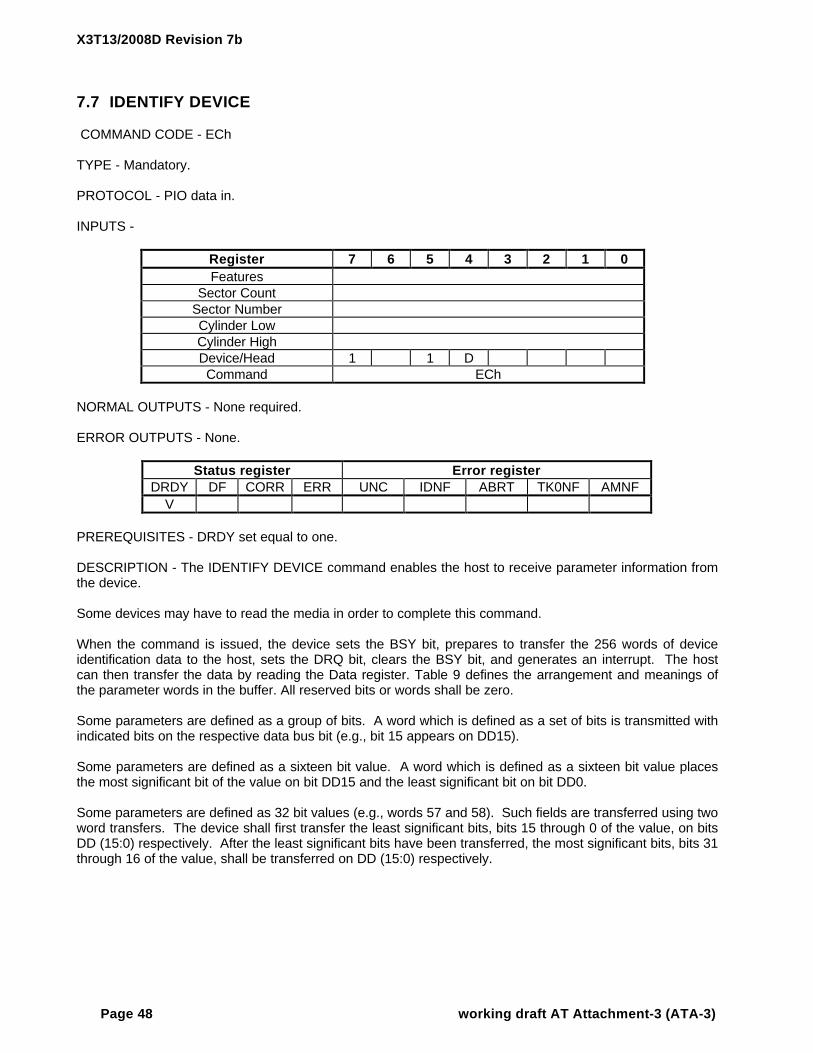
X3T13/2008D Revision 7b
Page 48 working draft AT Attachment-3 (ATA-3)
7.7 IDENTIFY DEVICE
COMMAND CODE - ECh
TYPE - Mandatory.
PROTOCOL - PIO data in.
INPUTS -
Register 7 6 5 4 3 2 1 0Features
Sector CountSector NumberCylinder LowCylinder HighDevice/Head 1 1 DCommand ECh
NORMAL OUTPUTS - None required.
ERROR OUTPUTS - None.
Status register Error registerDRDY DF CORR ERR UNC IDNF ABRT TK0NF AMNF
V
PREREQUISITES - DRDY set equal to one.
DESCRIPTION - The IDENTIFY DEVICE command enables the host to receive parameter information fromthe device.
Some devices may have to read the media in order to complete this command.
When the command is issued, the device sets the BSY bit, prepares to transfer the 256 words of deviceidentification data to the host, sets the DRQ bit, clears the BSY bit, and generates an interrupt. The hostcan then transfer the data by reading the Data register. Table 9 defines the arrangement and meanings ofthe parameter words in the buffer. All reserved bits or words shall be zero.
Some parameters are defined as a group of bits. A word which is defined as a set of bits is transmitted withindicated bits on the respective data bus bit (e.g., bit 15 appears on DD15).
Some parameters are defined as a sixteen bit value. A word which is defined as a sixteen bit value placesthe most significant bit of the value on bit DD15 and the least significant bit on bit DD0.
Some parameters are defined as 32 bit values (e.g., words 57 and 58). Such fields are transferred using twoword transfers. The device shall first transfer the least significant bits, bits 15 through 0 of the value, on bitsDD (15:0) respectively. After the least significant bits have been transferred, the most significant bits, bits 31through 16 of the value, shall be transferred on DD (15:0) respectively.

X3T13/2008D Revision 7b
working draft AT Attachment-3 (ATA-3) Page 49
Some parameters are defined as a string of ASCII characters. For the string “Copyright”, the character “C” isthe first byte, “o” is the 2nd byte, etc. When such fields are transferred, the order of transmission is:
the 1st character (“C”) is on bits DD (15:8) of the first word; the 2nd character (“o”) is on bits DD (7:0) of the first word; the 3rd character (“p”) is on bits DD (15:8) of the second word; the 4th character (“y”) is on bits DD (7:0) of the second word; etc.
Table 9 −− Identify device informationWord F/V
0 General configuration bit-significant information:F
FFFFFFFFFFFFFFF
15
14131211109876543210
0=ATA device1=ATAPI deviceObsoleteObsoleteObsoleteObsoleteObsoleteObsoleteObsolete1=removable media device1=not removable controller and/or deviceObsoleteObsoleteObsoleteObsoleteObsoleteReserved
1 F Number of logical cylinders2 R Reserved3 F Number of logical heads4 X Obsolete5 X Obsolete6 F Number of logical sectors per logical track
7-9 X Vendor specific10-19 F Serial number (20 ASCII characters)
20 X Obsolete21 X Obsolete22 F Number of vendor specific bytes available on READ/WRITE LONG cmds
23-26 F Firmware revision (8 ASCII characters)27-46 F Model number (40 ASCII characters)
47 XRF
15-87-0
Vendor specific00h =Reserved01h-FFh = Maximum number of sectors that can be transferred per interrupt on READ/WRITE MULTIPLE commands
48 R Reserved(continued)

X3T13/2008D Revision 7b
Page 50 working draft AT Attachment-3 (ATA-3)
Table 9 −− Identify device information (continued)Word F/V
49 CapabilitiesRF
RF
FRRX
15-1413
1211
1098
7-0
Reserved1=Standby timer values as specified in this standard are supported0=Standby timer values are vendor specificReserved (for advanced transfer mode)1=IORDY supported0=IORDY may be supported1=IORDY can be disabledObsoleteObsoleteVendor specific
50 R Reserved51 F
X15-87-0
PIO data transfer cycle timing modeVendor specific
52 RX
15-87-0
ObsoleteVendor specific
53 RFFVV
15-21
0
Reserved1=the fields reported in words 64-70 are valid0=the fields reported in words 64-70 are not valid1=the fields reported in words 54-58 are valid0=the fields reported in words 54-58 may be valid
54 V Number of current logical cylinders55 V Number of current logical heads56 V Number of current logical sectors per track
57-58 V Current capacity in sectors59 R
VV
15-98
7-0
Reserved1=Multiple sector setting is validxxh=Current setting for number of sectors that can be transferred per interrupt on R/W Multiple command
60-61 F Total number of user addressable sectors (LBA mode only)62 R Obsolete63 V
F15-87-0
Multiword DMA transfer mode activeMultiword DMA transfer modes supported
64 RF
15-87-0
ReservedAdvanced PIO transfer modes supported
65 Minimum Multiword DMA transfer cycle time per wordF 15-0 Cycle time in nanoseconds
66 Manufacturer’s recommended Multiword DMA transfer cycle timeF 15-0 Cycle time in nanoseconds
67 Minimum PIO transfer cycle time without flow controlF 15-0 Cycle time in nanoseconds
68 Minimum PIO transfer cycle time with IORDY flow controlF 15-0 Cycle time in nanoseconds
69-79 R Reserved (for future command overlap and queuing)(continued)

X3T13/2008D Revision 7b
working draft AT Attachment-3 (ATA-3) Page 51
Table 9 −− Identify device information (concluded)Word F/V
80 F Major version number0000h or FFFFh = device does not report version
151413121110987654321
ReservedReserved for ATA-14Reserved for ATA-13Reserved for ATA-12Reserved for ATA-11Reserved for ATA-10Reserved for ATA-9Reserved for ATA-8Reserved for ATA-7Reserved for ATA-6Reserved for ATA-5Reserved for ATA-41=supports ATA-31=supports ATA-21=supports ATA-1
81 F Minor version number0000h or FFFFh=device does not report version0001h-FFFEh=see 7.7.37
82 F Command set supported. If words 82 and 83 =0000h or FFFFh command setnotification not supported.15-4
3210
Reserved1=supports power management feature set1=supports removeable feature set1=supports security feature set1=supports SMART feature set
83 F Command sets supported. If words 82 and 83 =0000h or FFFFh command setnotification not supported.
1514
13-0
Shall be cleared to zero.Shall be set to oneReserved
84-127 R Reserved128 V Security status
15-98
7-543210
ReservedSecurity level 0=High, 1=MaximumReserved1=Security count expired1=Security frozen1=Security locked1=Security enabled1=Security supported
129-159 X Vendor specific160-255 R Reserved
Key:F = the content of the word is fixed and does not change. For removable media devices, these values maychange when media is removed or changed.V = the contents of the word is variable and may change depending on the state of the device or thecommands executed by the device.X = the content of the word is vendor specific and may be fixed or variable.R = the content of the word is reserved and shall be zero.

X3T13/2008D Revision 7b
Page 52 working draft AT Attachment-3 (ATA-3)
7.7.1 Word 0: General configuration
Devices that conform to this standard shall clear bit 15 to zero. These values are shown to maintainalignment with the X3T10/1120 standard.
7.7.2 Word 1: Number of cylinders
The number of user-addressable logical cylinders in the default translation mode. If the value in Words 60and 61 exceed 16,515,072, this word shall contain 16,383 (see 6.2).
7.7.3 Word 2: Reserved.
7.7.4 Word 3: Number of logical heads
The number of user-addressable logical heads per logical cylinder in the default translation mode. If thevalue in Words 60 and 61 exceed 16,515,072, this word shall contain 16 (see 6.2).
7.7.5 Word 4: Vendor specific data.
7.7.6 Word 5: Vendor specific data.
7.7.7 Word 6: Number of logical sectors per logical track
The number of user-addressable logical sectors per logical track in the default translation mode. If the valuein Words 60 and 61 exceed 16,515,072, this word shall contain 63 (see 6.2).
7.7.8 Words 7-9: Vendor specific data.
7.7.9 Words 10-19: Serial number
This field contains the serial number of the device. The contents of this field is an ASCII character string oftwenty bytes. The device shall pad the character string with spaces (20h), if necessary, to ensure that thestring is the proper length. The combination of Serial number (Words 10-19) and Model number (Words 27-46) shall be unique.
7.7.10 Word 20: Vendor specific data.
7.7.11 Word 21: Vendor specific data.
7.7.12 Word 22: Number of vendor specific bytes on READ/WRITE LONG commands
The contents of this field specifies the number of vendor specific bytes that are appropriate for the device. Ifthe contents of this field are set to a value other than 4, the SET FEATURES command should be used toswitch the length of READ LONG and WRITE LONG commands from 512 plus 4 to 512 plus the valuespecified in this word.
7.7.13 Word 23-26: Firmware revision
If word 23 of this field is 0000h, then the firmware revision is not specified and the definition of the remainingwords of this field are vendor specific.
If word 23 of this field is not equal to 0000h, then this field contains the firmware revision of the device. Thecontents of this field is an ASCII character string of eight bytes. The device shall pad the character stringwith spaces (20h), if necessary, to ensure that the string is the proper length.

X3T13/2008D Revision 7b
working draft AT Attachment-3 (ATA-3) Page 53
7.7.14 Words 27-46: Model number
This field contains the model number of the device. The contents of this field is an ASCII character string offorty bytes. The device shall pad the character string with spaces (20h), if necessary, to ensure that thestring is the proper length. The combination of Serial number (Words 10-19) and Model number (Words 27-46) shall be unique.
7.7.15 Word 47: READ/WRITE MULTIPLE support.
Bits 7-0 of this word define the maximum number of sectors per block that the device supports forREAD/WRITE MULTIPLE commands.
7.7.16 Word 48: Reserved.
7.7.17 Word 49: Capabilities
7.7.17.1 Standby timer support
Bit 13 of word 49 is used to determine whether a device utilizes the Standby Timer Values as defined in thisstandard. Table 11 specifies the Standby Timer values utilized by the device if bit 13 is set to one. If bit 13 iscleared to zero, the timer values utilized are vendor specific.
7.7.17.2 IORDY support
Bit 11 of word 49 is used to help determine whether a device supports IORDY. If this bit is set to one, thenthe device supports IORDY operation. If this bit is zero, the device may support IORDY. This ensuresbackward compatibility. If a device supports PIO Mode 3, then this bit shall be set.
7.7.17.3 IORDY can be disabled
Bit 10 of word 49 is used to indicate a device’s ability to enable or disable the use of IORDY. If this bit is setto one, then the device supports the disabling of IORDY. Control of IORDY is accomplished using the SETFEATURES command.
7.7.17.4 Obsolete
Bits 8 and 9 of word 49 are obsolete.
7.7.18 Word 50: Reserved
7.7.19 Word 51: PIO data transfer cycle timing mode
The PIO transfer timing for each ATA device falls into categories which have unique parametric timingspecifications. To determine the proper device timing category, compare the Cycle Time specified in 9.4.2with the contents of this field. The value returned in Bits 15-8 should fall into one of the mode 0 throughmode 2 categories specified in 9.4.2, and if it does not, then Mode 0 shall be used to serve as the defaulttiming.
NOTE − For backwards compatibility with BIOSs written before Word 64 was defined foradvanced modes, a device reports in Word 51 the highest original PIO mode (i.e. PIO mode0, 1, or 2) it can support.
7.7.20 Word 52: Obsolete

X3T13/2008D Revision 7b
Page 54 working draft AT Attachment-3 (ATA-3)
7.7.21 Word 53: Field validity
If bit 0 of word 53 is set, then the values reported in words 54 through 58 are valid. If this bit is cleared, thevalues reported in words 54 through 58 may be valid. If bit 1 of word 53 is set, then the values reported inwords 64 through 70 are valid. If this bit is cleared, the values reported in words 64-70 are not valid. Anydevice which supports PIO Mode 3 or above, or supports Multiword DMA Mode 1 or above, shall set bit 1 ofword 53 and support the fields contained in words 64 through 70.
7.7.22 Word 54: Number of current logical cylinders
The number of user-addressable logical cylinders in the current translation mode.
NOTE − For ATA-1 devices, if the INITIALIZE DEVICE PARAMETERS command has notbeen issued to the device then the value of this word is vendor specific.
7.7.23 Word 55: Number of current logical heads
The number of user-addressable logical heads per logical cylinder in the current translation mode.
NOTE − For ATA-1 devices, if the INITIALIZE DEVICE PARAMETERS command has notbeen issued to the device then the value of this word is vendor specific.
7.7.24 Word 56: Number of current logical sectors per logical track
The number of user-addressable logical sectors per logical track in the current translation mode.
NOTE − For ATA-1 devices, if the INITIALIZE DEVICE PARAMETERS command has notbeen issued to the device then the value of this word is vendor specific.
7.7.25 Word 57-58: Current capacity in sectors
The current capacity in sectors excludes all sectors used for device-specific purposes. The value reported inthis field shall be the product of words 54, 55, and 56.
7.7.26 Word 59: Multiple sector setting
If bit 8 is set, then bits 7-0 reflect the number of sectors currently set to transfer on a READ/WRITEMULTIPLE command. If word 47 bits 7-0 are zero then word 59 bits 8-0 shall also be zero. This field maybe defaulted to the optimum value.
7.7.27 Word 60-61: Total number of user addressable sectors
These words reflect the total number of user addressable sectors in LBA translation. This value does notdepend on the current device geometry
7.7.28 Word 62:Obsolete
7.7.29 Word 63: Multiword DMA transfer
The low order byte identifies by bit all of the Modes which are supported, e.g., if Mode 0 is supported, bit 0 isset to one. The high order byte contains a single bit set to indicate which mode is active supported, e.g., ifMode 0 is active, bit 0 is set to one.

X3T13/2008D Revision 7b
working draft AT Attachment-3 (ATA-3) Page 55
7.7.30 Word 64: Flow control PIO transfer modes supported
Bits 7 through 0 of word 64 of the Identify Device parameter information is defined as the Advanced PIOData Transfer Supported Field. This field is bit significant. Any number of bits may be set in this field by thedevice to indicate which Advanced PIO Modes it is capable of supporting.
Of these bits, bits 7 through 2 are Reserved for future Advanced PIO Modes. Bit 0, if set, indicates that thedevice supports PIO Mode 3. Bit 1, if set, indicates that the device supports PIO Mode 4.
NOTE − For backwards compatibility with BIOSs written before Word 64 was defined foradvanced modes, a device reports in Word 51 the highest original PIO mode (i.e. PIO mode0, 1, or 2) it can support.
7.7.31 Word 65: Minimum multiword DMA transfer cycle time per word
Word 65 of the parameter information of the IDENTIFY DEVICE command is defined as the MinimumMultiword DMA Transfer Cycle Time Per Word. This field defines, in nanoseconds, the minimum cycle timethat the device can support when performing Multiword DMA transfers on a per word basis.
If this field is supported, bit 1 of word 53 shall be set. Any device which supports Multiword DMA Mode 1 orabove shall support this field, and the value in word 65 shall not be less than the minimum cycle time for thefastest DMA mode supported by the device.
If bit 1 of word 53 is set because a device supports a field in Words 64-70 other than this field and the devicedoes not support this field, the device shall return a value of zero in this field.
7.7.32 Word 66: Device recommended multiword DMA cycle time
Word 66 of the parameter information of the IDENTIFY DEVICE command is defined as the DeviceRecommended Multiword DMA Transfer Cycle Time. This field defines, in nanoseconds, the minimum cycletime per word during a single sector host transfer while performing a multiple sector READ DMA or WRITEDMA command over all locations on the media under nominal conditions. If a host runs at a faster cycle rateby operating at a cycle time of less than this value, the device may negate DMARQ for flow control. Therate at which DMARQ is negated could result in reduced throughput despite the faster cycle rate. Transferat this rate does not ensure that flow control will not be used, but implies that higher performance may result.
If this field is supported, bit 1 of word 53 shall be set. Any device which supports Multiword DMA Mode 1 orabove shall support this field, and the value in word 66 shall not be less than the value in word 65.
If bit 1 of word 53 is set because a device supports a field in Words 64-70 other than this field and the devicedoes not support this field, the device shall return a value of zero in this field.
7.7.33 Word 67: Minimum PIO transfer cycle time without flow control
Word 67 of the parameter information of the IDENTIFY DEVICE command is defined as the Minimum PIOTransfer Without Flow Control Cycle Time. This field defines, in nanoseconds, the minimum cycle time that,if used by the host, the device guarantees data integrity during the transfer without utilization of flow control.
Any device may support this field, and if this field is supported, Bit 1 of word 53 shall be set.
Any device which supports PIO Mode 3 or above shall support this field, and the value in word 67 shall notbe less than the value reported in word 68.
If bit 1 of word 53 is set because a device supports a field in Words 64-70 other than this field and the devicedoes not support this field, the device shall return a value of zero in this field.

X3T13/2008D Revision 7b
Page 56 working draft AT Attachment-3 (ATA-3)
7.7.34 Word 68: Minimum PIO transfer cycle time with IORDY
Word 68 of the parameter information of the IDENTIFY DEVICE command is defined as the Minimum PIOTransfer With IORDY Flow Control Cycle Time. This field defines, in nanoseconds, the minimum cycle timethat the device can support while performing data transfers while utilizing IORDY flow control.
Any device may support this field, and if this field is supported, Bit 1 of word 53 shall be set.
Any device which supports PIO Mode 3 or above shall support this field, and the value in word 68 shall notbe less than the fastest PIO mode reported by the device.
If bit 1 of word 53 is set because a device supports a field in Words 64-70 other than this field and the devicedoes not support this field, the device shall return a value of zero in this field.
7.7.35 Words 69-79: Reserved
Words 69 through 79 are reserved for future command overlap and queuing.
7.7.36 Word 80: Major version number
If not 0000h or FFFFh, the device claims compliance with the major version(s) as indicated by bits 1 through3 being equal to one. Values other than 0000h and FFFFh are bit significant. Since the ATA-3 and ATA-2standards maintain downward compatibility with ATA-1 (published as ATA), it is allowed for an ATA-3 deviceto set all of bits 1 through 3 to one.
7.7.37 Word 81: Minor version number
If an implementor claims that the revision of the standard they used to guide their implementation does notneed to be reported or if the implementation was based upon a standard prior to this revision of thestandard, Word 81 shall be 0000h or FFFFh.
Table 10 defines the value that may optionally be reported in Word 81 to indicate the revision of the standardwhich guided the implementation.
Table 10 −− Minor version numberValue Minor revision0001h ATA (ATA-1) X3T9.2 781D prior to revision 40002h ATA-1 published, ANSI X3.221-19940003h ATA (ATA-1) X3T9.2 781D revision 40004h ATA-2 published, ANSI X3.279-19960005h ATA-2 X3T10 948D prior to revision 2k0006h ATA-3 X3T10 2008D revision 10007h ATA-2 X3T10 948D revision 2k0008h ATA-3 X3T10 2008D revision 00009h ATA-2 X3T10 948D revision 3000Ah ATA-3 published, ANSI X3.298-1997000Bh ATA-3 X3T10 2008D revision 6000Ch ATA-3 X3T13 2008D revision 7
000Dh-FFFFh Reserved

X3T13/2008D Revision 7b
working draft AT Attachment-3 (ATA-3) Page 57
7.7.38 Words 82-83: Command sets supported
Words 82 and 83 indicate command sets supported. The values 0000h and FFFFh in these words indicatethat command set support is not indicated. Bits 4 through 15 of Word 82 are reserved. Bits 0 through 13 ofWord 83 are reserved. Bit 14 of Word 83 shall be set to one. Bit 15 of Word 83 shall be cleared to zero.
If bit 0 of Word 82 is set, the SMART feature set is supported.
If bit 1 of Word 82 is set, the security feature set is supported.
If bit 2 of Word 82 is set, the removable feature set is supported.
If bit 3 of Word 82 is set, the power management feature set is supported.
7.7.39 Words 84-127: Reserved.
7.7.40 Word 128: Security status
7.7.40.1 Security level
Bit 8 of Word 128 indicates the security level. If bit 8 is cleared to zero, the security level is high. If bit 8 is setto one, the security level is maximum. When security mode is disabled, bit 8 is cleared to zero.
7.7.40.2 Security count expired
Bit 4 of Word 128 indicates that the security count has expired. If bit 4 is set to one, the security count isexpired and SECURITY UNLOCK and SECURITY ERASE UNIT are aborted until a power-on reset or hardreset.
7.7.40.3 Security frozen
Bit 3 of Word 128 indicates security frozen. If bit 3 is set to one, the security is frozen.
7.7.40.4 Security locked
Bit 2 of Word 128 indicates security locked. If bit 2 is set to one, the security is locked.
7.7.40.5 Security enabled
Bit 1 of Word 128 indicates security enabled. If bit 1 is set to one, the security is enabled.
7.7.40.6 Security supported
Bit 0 of Word 128 indicates Security mode feature set is supported. If bit 0 is set to one, security issupported.
7.7.41 Words 129-159: Vendor specific.
7.7.42 Words 160-255: Reserved.

X3T13/2008D Revision 7b
Page 58 working draft AT Attachment-3 (ATA-3)
7.8 IDENTIFY DEVICE DMA
COMMAND CODE - EEh
TYPE - Optional.
PROTOCOL - DMA.
INPUTS -
Register 7 6 5 4 3 2 1 0Features
Sector CountSector NumberCylinder LowCylinder HighDevice/Head 1 1 DCommand EEh
NORMAL OUTPUTS - None required.
ERROR OUTPUTS - None.
Status register Error registerDRDY DF CORR ERR UNC IDNF ABRT TK0NF AMNF
V
PREREQUISITES - DRDY set equal to one.
DESCRIPTION - The IDENTIFY DEVICE DMA command enables the host to receive parameter informationfrom the device in DMA mode. The command transfers the same 256 words of device identification data astransferred by the IDENTIFY DEVICE command.

X3T13/2008D Revision 7b
working draft AT Attachment-3 (ATA-3) Page 59
7.9 IDLE
COMMAND CODE - 97h or E3h
TYPE - Optional - Power Management Feature Set.
PROTOCOL - Non-data command.
INPUTS - The value in the Sector Count register when the IDLE command is issued shall determine the timeperiod programmed into the Standby Timer. Table 11 defines these values.
Register 7 6 5 4 3 2 1 0Features
Sector Count Timer period valueSector NumberCylinder LowCylinder HighDevice/Head 1 1 DCommand 97h or E3h
Table 11 −− Automatic standby timer periodsSector Count register
contentsCorresponding timeout period
0 (00h) Timeout disabled1-240 (01h-F0h) (value * 5) s
241-251 (F1h-FBh) ((value - 240) * 30) min252 (FCh) 21 min253 (FDh) Period between 8 and 12 hrs254 (FEh) Reserved255 (FFh) 21 min 15 s
Note: Times are approximate.
NORMAL OUTPUTS - None required.
ERROR OUTPUTS - Aborted Command - The device does not support the Power Management feature set.
Status register Error registerDRDY DF CORR ERR UNC IDNF ABRT TK0NF AMNF
V V V V
PREREQUISITES - DRDY set equal to one.
DESCRIPTION - This command causes the device to set the BSY bit, enter the Idle Mode, clear the BSYbit, and assert INTRQ. INTRQ is asserted even though the device may not have fully transitioned to IdleMode.
If the Sector Count register is non-zero then the Standby Timer shall be enabled. The value in the SectorCount register shall be used to determine the time programmed into the Standby Timer (see 6.3).
If the Sector Count register is zero then the Standby Timer is disabled.

X3T13/2008D Revision 7b
Page 60 working draft AT Attachment-3 (ATA-3)
7.10 IDLE IMMEDIATE
COMMAND CODE - 95h or E1h
TYPE - Optional - Power Management Feature Set.
PROTOCOL - Non-data command.
INPUTS -
Register 7 6 5 4 3 2 1 0Features
Sector CountSector NumberCylinder LowCylinder HighDevice/Head 1 1 DCommand 95h or E1h
NORMAL OUTPUTS - None required.
ERROR OUTPUTS - Aborted Command - The device does not support the Power Management feature set.
Status register Error registerDRDY DF CORR ERR UNC IDNF ABRT TK0NF AMNF
V V V V
PREREQUISITES - DRDY set equal to one.
DESCRIPTION - This command causes the device to set the BSY bit, enter the Idle Mode, clear the BSYbit, and assert INTRQ. INTRQ is asserted even though the device may not have fully transitioned to IdleMode (see 6.3).
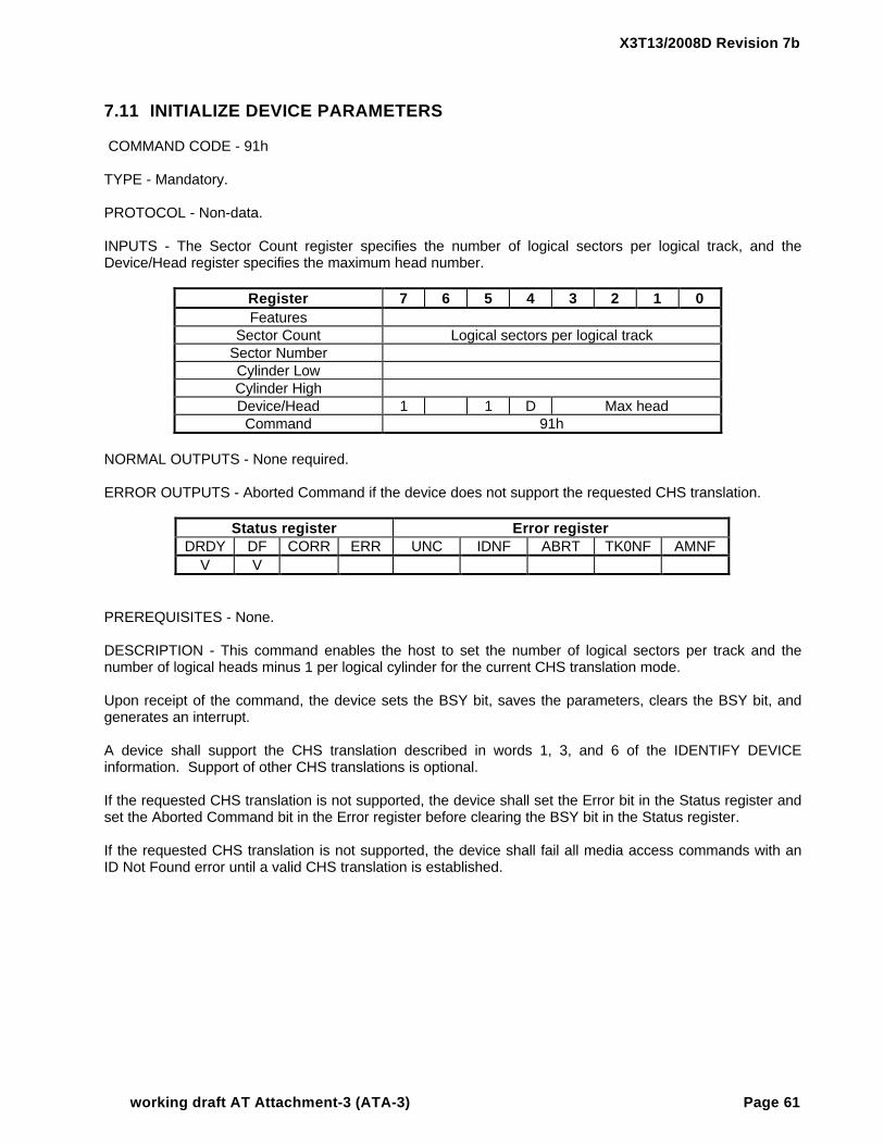
X3T13/2008D Revision 7b
working draft AT Attachment-3 (ATA-3) Page 61
7.11 INITIALIZE DEVICE PARAMETERS
COMMAND CODE - 91h
TYPE - Mandatory.
PROTOCOL - Non-data.
INPUTS - The Sector Count register specifies the number of logical sectors per logical track, and theDevice/Head register specifies the maximum head number.
Register 7 6 5 4 3 2 1 0Features
Sector Count Logical sectors per logical trackSector NumberCylinder LowCylinder HighDevice/Head 1 1 D Max headCommand 91h
NORMAL OUTPUTS - None required.
ERROR OUTPUTS - Aborted Command if the device does not support the requested CHS translation.
Status register Error registerDRDY DF CORR ERR UNC IDNF ABRT TK0NF AMNF
V V
PREREQUISITES - None.
DESCRIPTION - This command enables the host to set the number of logical sectors per track and thenumber of logical heads minus 1 per logical cylinder for the current CHS translation mode.
Upon receipt of the command, the device sets the BSY bit, saves the parameters, clears the BSY bit, andgenerates an interrupt.
A device shall support the CHS translation described in words 1, 3, and 6 of the IDENTIFY DEVICEinformation. Support of other CHS translations is optional.
If the requested CHS translation is not supported, the device shall set the Error bit in the Status register andset the Aborted Command bit in the Error register before clearing the BSY bit in the Status register.
If the requested CHS translation is not supported, the device shall fail all media access commands with anID Not Found error until a valid CHS translation is established.

X3T13/2008D Revision 7b
Page 62 working draft AT Attachment-3 (ATA-3)
7.12 MEDIA EJECT
COMMAND CODE - EDh
TYPE - Optional - Removable.
PROTOCOL - Non-data.
INPUTS -
Register 7 6 5 4 3 2 1 0Features
Sector CountSector NumberCylinder LowCylinder HighDevice/Head 1 1 DCommand EDh
NORMAL OUTPUTS - None required.
ERROR OUTPUTS - If the device does not support this command, the device shall return a Command Aborterror.
Status register Error registerDRDY DF CORR ERR UNC IDNF ABRT TK0NF AMNF
V V V V
PREREQUISITES - DRDY set equal to one.
DESCRIPTION - This command completes any pending operations, spins down the device if needed,unlocks the door or media if locked, and initiates a media eject, if required.

X3T13/2008D Revision 7b
working draft AT Attachment-3 (ATA-3) Page 63
7.13 NOP
COMMAND CODE - 00h
TYPE - Optional.
PROTOCOL - Non-data.
INPUTS -
Register 7 6 5 4 3 2 1 0Features
Sector CountSector NumberCylinder LowCylinder HighDevice/Head 1 1 DCommand 00h
NORMAL OUTPUTS - The Command Block registers, other than the Error and Status registers, are notchanged by this command. This command always fails with an Aborted Command error.
Status register Error registerDRDY DF CORR ERR UNC IDNF ABRT TK0NF AMNF
V V V V
ERROR OUTPUTS - None.
PREREQUISITES - DRDY set equal to one.
DESCRIPTION - This command enables a host, which can only perform 16-bit register accesses, to checkdevice status. The device shall respond, as it does to an unrecognized command, by setting AbortedCommand in the Error register, Error in the Status register, clearing Busy in the Status register, andasserting INTRQ.

X3T13/2008D Revision 7b
Page 64 working draft AT Attachment-3 (ATA-3)
7.14 READ BUFFER
COMMAND CODE - E4h
TYPE - Optional.
PROTOCOL - PIO data in.
INPUTS -
Register 7 6 5 4 3 2 1 0Features
Sector CountSector NumberCylinder LowCylinder HighDevice/Head 1 1 DCommand E4h
NORMAL OUTPUTS - None required.
ERROR OUTPUTS - Aborted Command if the command is not supported.
Status register Error registerDRDY DF CORR ERR UNC IDNF ABRT TK0NF AMNF
V V V V
PREREQUISITES - DRDY set equal to one. A WRITE BUFFER command shall immediately precede aREAD BUFFER command.
DESCRIPTION - The READ BUFFER command enables the host to read the current contents of thedevice’s sector buffer. When this command is issued, the device sets the BSY bit, sets up the sector bufferfor a read operation, sets the DRQ bit, clears the BSY bit, and generates an interrupt. The host then readsthe data from the buffer.
The READ BUFFER and WRITE BUFFER commands shall be synchronized such that sequential WRITEBUFFER and READ BUFFER commands access the same 512 bytes within the buffer.

X3T13/2008D Revision 7b
working draft AT Attachment-3 (ATA-3) Page 65
7.15 READ DMA (with retries and without retries)
COMMAND CODE - C8h (with retries) or C9h (without retries)
TYPE - Mandatory.
PROTOCOL - DMA.
INPUTS - The Cylinder Low, Cylinder High, Device/Head, and Sector Number registers specify the startingsector address to be read. The Sector Count register specifies the number of sectors to be transferred.
NORMAL OUTPUTS - None required.
Register 7 6 5 4 3 2 1 0Features
Sector Count Sector countSector Number Sector number or LBACylinder Low Cylinder low or LBACylinder High Cylinder high or LBADevice/Head 1 LBA 1 D Head number or LBACommand C8h or C9h
ERROR OUTPUTS - An unrecoverable error encountered during the execution of this command results inthe termination of the command and the Command Block registers contain the sector address of the sectorwhere the first unrecoverable error occurred. The amount of data transferred is indeterminant.
Status register Error registerDRDY DF CORR ERR UNC IDNF ABRT TK0NF AMNF
V V V V V V V V
PREREQUISITES - DRDY set equal to one. The host shall initialize the DMA channel.
DESCRIPTION - This command executes in a similar manner to the READ SECTOR(S) command exceptfor the following:
− the host initializes the DMA channel prior to issuing the command;− data transfers are qualified by DMARQ and are performed by the DMA channel;− the device issues only one interrupt per command to indicate that data transfer has terminated
and status is available.
During the DMA transfer phase of a READ DMA command, the device shall provide status of the BSY bit orthe DRQ bit until the command is completed.
Error recovery performed by the device either with or without retries is vendor specific.
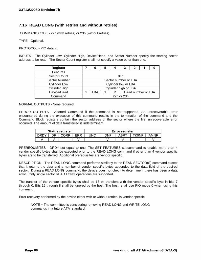
X3T13/2008D Revision 7b
Page 66 working draft AT Attachment-3 (ATA-3)
7.16 READ LONG (with retries and without retries)
COMMAND CODE - 22h (with retries) or 23h (without retries)
TYPE - Optional.
PROTOCOL - PIO data in.
INPUTS - The Cylinder Low, Cylinder High, Device/Head, and Sector Number specify the starting sectoraddress to be read. The Sector Count register shall not specify a value other than one.
Register 7 6 5 4 3 2 1 0Features
Sector Count 01hSector Number Sector number or LBACylinder Low Cylinder low or LBACylinder High Cylinder high or LBADevice/Head 1 LBA 1 D Head number or LBACommand 22h or 23h
NORMAL OUTPUTS - None required.
ERROR OUTPUTS - Aborted Command if the command is not supported. An unrecoverable errorencountered during the execution of this command results in the termination of the command and theCommand Block registers contain the sector address of the sector where the first unrecoverable erroroccurred. The amount of data transferred is indeterminant.
Status register Error registerDRDY DF CORR ERR UNC IDNF ABRT TK0NF AMNF
V V V V V V
PREREQUISITES - DRDY set equal to one. The SET FEATURES subcommand to enable more than 4vendor specific bytes shall be executed prior to the READ LONG command if other than 4 vendor specificbytes are to be transferred. Additional prerequisites are vendor specific.
DESCRIPTION - The READ LONG command performs similarly to the READ SECTOR(S) command exceptthat it returns the data and a number of vendor specific bytes appended to the data field of the desiredsector. During a READ LONG command, the device does not check to determine if there has been a dataerror. Only single sector READ LONG operations are supported.
The transfer of the vendor specific bytes shall be 16 bit transfers with the vendor specific byte in bits 7through 0. Bits 15 through 8 shall be ignored by the host. The host shall use PIO mode 0 when using thiscommand.
Error recovery performed by the device either with or without retries is vendor specific.
NOTE − The committee is considering removing READ LONG and WRITE LONGcommands in a future ATA standard.
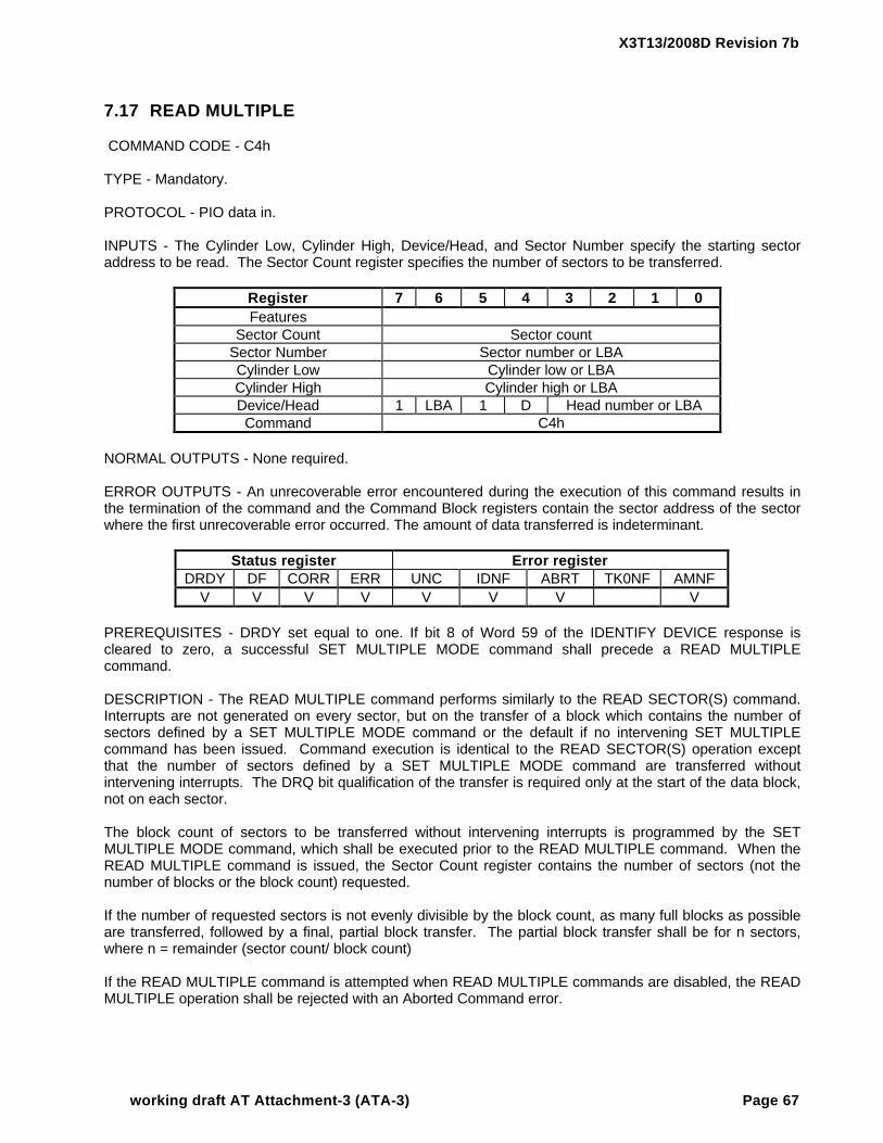
X3T13/2008D Revision 7b
working draft AT Attachment-3 (ATA-3) Page 67
7.17 READ MULTIPLE
COMMAND CODE - C4h
TYPE - Mandatory.
PROTOCOL - PIO data in.
INPUTS - The Cylinder Low, Cylinder High, Device/Head, and Sector Number specify the starting sectoraddress to be read. The Sector Count register specifies the number of sectors to be transferred.
Register 7 6 5 4 3 2 1 0Features
Sector Count Sector countSector Number Sector number or LBACylinder Low Cylinder low or LBACylinder High Cylinder high or LBADevice/Head 1 LBA 1 D Head number or LBACommand C4h
NORMAL OUTPUTS - None required.
ERROR OUTPUTS - An unrecoverable error encountered during the execution of this command results inthe termination of the command and the Command Block registers contain the sector address of the sectorwhere the first unrecoverable error occurred. The amount of data transferred is indeterminant.
Status register Error registerDRDY DF CORR ERR UNC IDNF ABRT TK0NF AMNF
V V V V V V V V
PREREQUISITES - DRDY set equal to one. If bit 8 of Word 59 of the IDENTIFY DEVICE response iscleared to zero, a successful SET MULTIPLE MODE command shall precede a READ MULTIPLEcommand.
DESCRIPTION - The READ MULTIPLE command performs similarly to the READ SECTOR(S) command.Interrupts are not generated on every sector, but on the transfer of a block which contains the number ofsectors defined by a SET MULTIPLE MODE command or the default if no intervening SET MULTIPLEcommand has been issued. Command execution is identical to the READ SECTOR(S) operation exceptthat the number of sectors defined by a SET MULTIPLE MODE command are transferred withoutintervening interrupts. The DRQ bit qualification of the transfer is required only at the start of the data block,not on each sector.
The block count of sectors to be transferred without intervening interrupts is programmed by the SETMULTIPLE MODE command, which shall be executed prior to the READ MULTIPLE command. When theREAD MULTIPLE command is issued, the Sector Count register contains the number of sectors (not thenumber of blocks or the block count) requested.
If the number of requested sectors is not evenly divisible by the block count, as many full blocks as possibleare transferred, followed by a final, partial block transfer. The partial block transfer shall be for n sectors,where n = remainder (sector count/ block count)
If the READ MULTIPLE command is attempted when READ MULTIPLE commands are disabled, the READMULTIPLE operation shall be rejected with an Aborted Command error.

X3T13/2008D Revision 7b
Page 68 working draft AT Attachment-3 (ATA-3)
Device errors encountered during READ MULTIPLE commands are posted at the beginning of the block orpartial block transfer, but the DRQ bit is still set and the data transfer shall take place as it normally would,including transfer of corrupted data, if any. The contents of the Command Block Registers following thetransfer of a data block which had a sector in error are undefined. The host should retry the transfer asindividual requests to obtain valid error information.
Subsequent blocks or partial blocks are transferred only if the error was a correctable data error. All othererrors cause the command to stop after transfer of the block which contained the error. Interrupts aregenerated when the DRQ bit is set at the beginning of each block or partial block.

X3T13/2008D Revision 7b
working draft AT Attachment-3 (ATA-3) Page 69
7.18 READ SECTOR(S) (with retries and without retries)
COMMAND CODE - 20h (with retries) or 21h (without retries)
TYPE - Mandatory.
PROTOCOL - PIO data in.
INPUTS - The Cylinder Low, Cylinder High, Device/Head, and Sector Number specify the starting sectoraddress to be read. The Sector Count register specifies the number of sectors to be transferred.
Register 7 6 5 4 3 2 1 0Features
Sector Count Sector countSector Number Sector number or LBACylinder Low Cylinder low or LBACylinder High Cylinder high or LBADevice/Head 1 LBA 1 D Head number or LBACommand 20h or 21h
NORMAL OUTPUTS - None required.
ERROR OUTPUTS - An unrecoverable error encountered during the execution of this command results inthe termination of the command and the Command Block registers contain the sector address of the sectorwhere the first unrecoverable error occurred. The amount of data transferred is indeterminant.
Status register Error registerDRDY DF CORR ERR UNC IDNF ABRT TK0NF AMNF
V V V V V V V V
PREREQUISITES - DRDY set equal to one.
DESCRIPTION - This command reads from 1 to 256 sectors as specified in the Sector Count register. Asector count of 0 requests 256 sectors. The transfer begins at the sector specified in the Sector Numberregister.
The DRQ bit is always set prior to data transfer regardless of the presence or absence of an error condition.
Error recovery performed by the device either with or without retries is vendor specific.

X3T13/2008D Revision 7b
Page 70 working draft AT Attachment-3 (ATA-3)
7.19 READ VERIFY SECTOR(S) (with retries and without retries)
COMMAND CODE - 40h (with retries) or 41h (without retries)
TYPE - Mandatory.
PROTOCOL - Non-data.
INPUTS - The Cylinder Low, Cylinder High, Device/Head, and Sector Number specify the starting sectoraddress to be verified. The Sector Count register specifies the number of sectors to be verified.
Register 7 6 5 4 3 2 1 0Features
Sector Count Sector countSector Number Sector number or LBACylinder Low Cylinder low or LBACylinder High Cylinder high or LBADevice/Head 1 LBA 1 D Head number or LBACommand 40h or 41h
NORMAL OUTPUTS - None required.
ERROR OUTPUTS - An unrecoverable error encountered during the execution of this command results inthe termination of the command and the Command Block registers contain the sector address of the sectorwhere the first unrecoverable error occurred.
Status register Error registerDRDY DF CORR ERR UNC IDNF ABRT TK0NF AMNF
V V V V V V V V
PREREQUISITES - DRDY set equal to one.
DESCRIPTION - This command is identical to the READ SECTOR(S) command, except that the DRQ bit isnever set, and no data is transferred to the host.
When the requested sectors have been verified, the device clears the BSY bit and generates an interrupt.
Error recovery performed by the device either with or without retries is vendor specific.

X3T13/2008D Revision 7b
working draft AT Attachment-3 (ATA-3) Page 71
7.20 RECALIBRATE
COMMAND CODE - 10h
TYPE - Optional.
PROTOCOL - Non-data.
INPUTS -
Register 7 6 5 4 3 2 1 0Features
Sector CountSector NumberCylinder LowCylinder HighDevice/Head 1 1 DCommand 10h
NORMAL OUTPUTS - If the command is executed in CHS addressing, Cylinder High, Cylinder Low, and thehead portion of Device/Head shall be zero. The Sector Number register shall be 1. If the command isexecuted in LBA addressing, the Cylinder High, Cylinder Low, the head portion of the Device/Head, and theSector Number register shall be zero.
ERROR OUTPUTS - If the device cannot reach cylinder 0, a Track 0 Not Found error is posted.
Status register Error registerDRDY DF CORR ERR UNC IDNF ABRT TK0NF AMNF
V V V V V
PREREQUISITES - DRDY set equal to one.
DESCRIPTION - The function performed by this command is vendor specific.

X3T13/2008D Revision 7b
Page 72 working draft AT Attachment-3 (ATA-3)
7.21 SECURITY DISABLE PASSWORD
COMMAND CODE - F6h
TYPE - Optional - Security mode feature set.
PROTOCOL - PIO data out.
INPUTS -
Register 7 6 5 4 3 2 1 0Features
Sector CountSector NumberCylinder LowCylinder HighDevice/Head 1 1 DCommand F6h
NORMAL OUTPUTS - None.
ERROR OUTPUTS - Device returns Aborted command error if command is not supported, the device is inLocked mode, or the device is in Frozen mode.
Status register Error registerDRDY DF CORR ERR UNC IDNF ABRT TK0NF AMNF
V V V V
PREREQUISITES - Device shall be in Unlocked mode.
DESCRIPTION - The SECURITY DISABLE PASSWORD command requests a transfer of a single sector ofdata from the host. Table 12 defines the content of this sector of information. Then the device checks thetransferred password. If the User password or the Master password match, the device disables the lockfunction. This command does not change the Master password which may be reactivated later by setting aUser password.
Table 12 −− Security password contentWord Content
0 Control wordBit 0 Identifier 0=compare user password
1=compare master passwordBit 1-15 Reserved
1-16 Password (32 bytes)17-255 Reserved

X3T13/2008D Revision 7b
working draft AT Attachment-3 (ATA-3) Page 73
7.22 SECURITY ERASE PREPARE
COMMAND CODE - F3h
TYPE - Optional - Security mode feature set.
PROTOCOL - Non-data.
INPUTS -
Register 7 6 5 4 3 2 1 0Features
Sector CountSector NumberCylinder LowCylinder HighDevice/Head 1 1 DCommand F3h
NORMAL OUTPUTS - None.
ERROR OUTPUTS - Device returns Aborted command error if command is not supported or the device is inFrozen mode.
Status register Error registerDRDY DF CORR ERR UNC IDNF ABRT TK0NF AMNF
V V V V
PREREQUISITES - None.
DESCRIPTION - The SECURITY ERASE PREPARE command shall be issued immediately before theSECURITY ERASE UNIT command to enable device erasing and unlocking. This command is to preventaccidental erasure of the device.
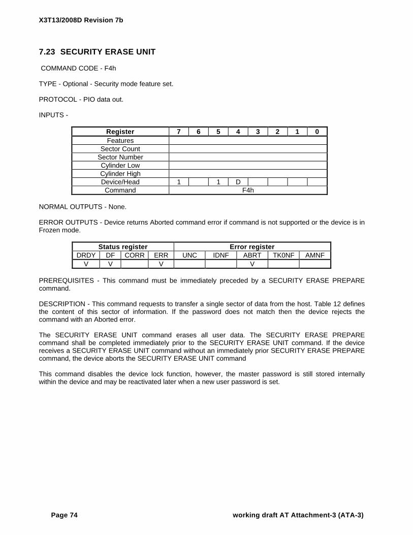
X3T13/2008D Revision 7b
Page 74 working draft AT Attachment-3 (ATA-3)
7.23 SECURITY ERASE UNIT
COMMAND CODE - F4h
TYPE - Optional - Security mode feature set.
PROTOCOL - PIO data out.
INPUTS -
Register 7 6 5 4 3 2 1 0Features
Sector CountSector NumberCylinder LowCylinder HighDevice/Head 1 1 DCommand F4h
NORMAL OUTPUTS - None.
ERROR OUTPUTS - Device returns Aborted command error if command is not supported or the device is inFrozen mode.
Status register Error registerDRDY DF CORR ERR UNC IDNF ABRT TK0NF AMNF
V V V V
PREREQUISITES - This command must be immediately preceded by a SECURITY ERASE PREPAREcommand.
DESCRIPTION - This command requests to transfer a single sector of data from the host. Table 12 definesthe content of this sector of information. If the password does not match then the device rejects thecommand with an Aborted error.
The SECURITY ERASE UNIT command erases all user data. The SECURITY ERASE PREPAREcommand shall be completed immediately prior to the SECURITY ERASE UNIT command. If the devicereceives a SECURITY ERASE UNIT command without an immediately prior SECURITY ERASE PREPAREcommand, the device aborts the SECURITY ERASE UNIT command
This command disables the device lock function, however, the master password is still stored internallywithin the device and may be reactivated later when a new user password is set.

X3T13/2008D Revision 7b
working draft AT Attachment-3 (ATA-3) Page 75
7.24 SECURITY FREEZE LOCK
COMMAND CODE - F5h
TYPE - Optional - Security mode feature set.
PROTOCOL - Non-data.
INPUTS -
Register 7 6 5 4 3 2 1 0Features
Sector CountSector NumberCylinder LowCylinder HighDevice/Head 1 1 DCommand F5h
NORMAL OUTPUTS - None.
ERROR OUTPUTS - Device returns Aborted command error if command is not supported, or the device is inLocked mode.
Status register Error registerDRDY DF CORR ERR UNC IDNF ABRT TK0NF AMNF
V V V V
PREREQUISITES - None
DESCRIPTION - The SECURITY FREEZE LOCK command sets the device to frozen mode. After thiscommand is completed any other commands which update the device lock functions are rejected. Frozenmode is quit by power off or hardware reset. If SECURITY FREEZE LOCK is issued when the device is infrozen mode, the command executes and the device remains in frozen mode.
Commands disabled by SECURITY FREEZE LOCK are:− SECURITY SET PASSWORD− SECURITY UNLOCK− SECURITY DISABLE PASSWORD− SECURITY ERASE UNIT

X3T13/2008D Revision 7b
Page 76 working draft AT Attachment-3 (ATA-3)
7.25 SECURITY SET PASSWORD
COMMAND CODE - F1h
TYPE - Optional - Security mode feature set.
PROTOCOL - PIO data out.
INPUTS -
Register 7 6 5 4 3 2 1 0Features
Sector CountSector NumberCylinder LowCylinder HighDevice/Head 1 1 DCommand F1h
NORMAL OUTPUTS - None.
ERROR OUTPUTS - Device returns Aborted command error if command is not supported, the device is inLocked mode, or the device is in Frozen mode.
Status register Error registerDRDY DF CORR ERR UNC IDNF ABRT TK0NF AMNF
V V V V
PREREQUISITES - None.
DESCRIPTION - This command requests a transfer of a single sector of data from the host. Table 13defines the content of this sector of information. The data transferred controls the function of this command.
Table 13 −− SECURITY SET PASSWORD data contentWord Content
0 Control wordBit 0
Bits 1-7Bit 8
Bits 9-15
Identifier
ReservedSecurity level
Reserved
0=set user password1=set master password
0=High1=Maximum
1-16 Password (32 bytes)17-255 Reserved
Table 14 defines the interaction of the identifier and security level bits.

X3T13/2008D Revision 7b
working draft AT Attachment-3 (ATA-3) Page 77
Table 14 −− Identifier and security level bit interactionIdentifie
rLevel Command result
User High The password supplied with the command shall be saved as the new userpassword. The lock function shall be enabled from the next power-on or hardwarereset. The device shall then be unlocked by either the user password or thepreviously set master password.
User Maximum The password supplied with the command shall be saved as the new userpassword. The lock function shall be enabled from the next power-on or hardwarereset. The device shall then be unlocked by only the user password. The masterpassword previously set is still stored in the device but shall not be used to unlockthe device.
Master High orMaximum
This combination shall set a master password but shall not enable or disable thelock function. The security level is not changed.

X3T13/2008D Revision 7b
Page 78 working draft AT Attachment-3 (ATA-3)
7.26 SECURITY UNLOCK
COMMAND CODE - F2h
TYPE - Optional - Security mode feature set.
PROTOCOL - PIO data out.
INPUTS -
Register 7 6 5 4 3 2 1 0Features
Sector CountSector NumberCylinder LowCylinder HighDevice/Head 1 1 DCommand F2h
NORMAL OUTPUTS - None.
ERROR OUTPUTS - Device returns Aborted command error if command is not supported, or the device is inFrozen mode.
Status register Error registerDRDY DF CORR ERR UNC IDNF ABRT TK0NF AMNF
V V V V
PREREQUISITES - None.
DESCRIPTION - This command requests to transfer a single sector of data from the host. Table 12 definesthe content of this sector of information.
If the Identifier bit is set to master and the device is in high security level, then the password supplied shallbe compared with the stored master password. If the device is in maximum security level then the unlockshall be rejected.
If the Identifier bit is set to user then the device compares the supplied password with the stored userpassword.
If the password compare fails then the device returns an abort error to the host and decrements the unlockcounter. This counter is initially set to five and is decremented for each password mismatch whenSECURITY UNLOCK is issued and the device is locked. When this counter reaches zero then SECURITYUNLOCK and SECURITY ERASE UNIT commands are aborted until a power-on reset or a hard reset.SECURITY UNLOCK commands issued when the device is unlocked have no effect on the unlock counter.

X3T13/2008D Revision 7b
working draft AT Attachment-3 (ATA-3) Page 79
7.27 SEEK
COMMAND CODE - 70h
TYPE - Mandatory.
PROTOCOL - Non-data.
INPUTS - The Cylinder High, Cylinder Low, head portion of the Device/Head register and the Sector Numberregister contain the sector address to which the device may move the read/write heads.
Register 7 6 5 4 3 2 1 0Features
Sector CountSector Number Sector number or LBACylinder Low Cylinder low or LBACylinder High Cylinder high or LBADevice/Head 1 LBA 1 D Head number or LBACommand 70h
NORMAL OUTPUTS - None required.
ERROR OUTPUTS - Error reporting is vendor specific.
Status register Error registerDRDY DF CORR ERR UNC IDNF ABRT TK0NF AMNF
V V V V V
PREREQUISITES - DRDY set equal to one.
DESCRIPTION - The function performed by this command is vendor specific, and may or may not affect theposition of the read/write heads.
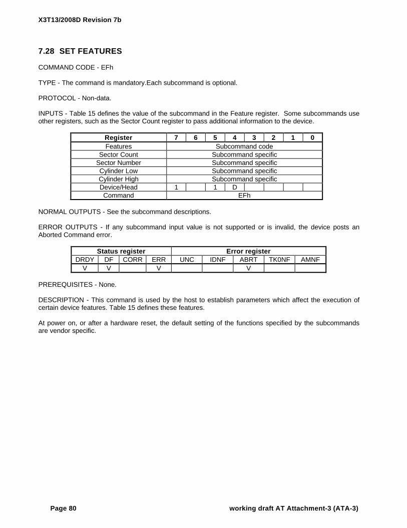
X3T13/2008D Revision 7b
Page 80 working draft AT Attachment-3 (ATA-3)
7.28 SET FEATURES
COMMAND CODE - EFh
TYPE - The command is mandatory.Each subcommand is optional.
PROTOCOL - Non-data.
INPUTS - Table 15 defines the value of the subcommand in the Feature register. Some subcommands useother registers, such as the Sector Count register to pass additional information to the device.
Register 7 6 5 4 3 2 1 0Features Subcommand code
Sector Count Subcommand specificSector Number Subcommand specificCylinder Low Subcommand specificCylinder High Subcommand specificDevice/Head 1 1 DCommand EFh
NORMAL OUTPUTS - See the subcommand descriptions.
ERROR OUTPUTS - If any subcommand input value is not supported or is invalid, the device posts anAborted Command error.
Status register Error registerDRDY DF CORR ERR UNC IDNF ABRT TK0NF AMNF
V V V V
PREREQUISITES - None.
DESCRIPTION - This command is used by the host to establish parameters which affect the execution ofcertain device features. Table 15 defines these features.
At power on, or after a hardware reset, the default setting of the functions specified by the subcommandsare vendor specific.

X3T13/2008D Revision 7b
working draft AT Attachment-3 (ATA-3) Page 81
Table 15 −− SET FEATURES register definitionsValue(seenote)01h Obsolete02h Enable write cache03h Set transfer mode based on value in Sector Count register. Table 16 defines values.04h Enable all automatic defect reassignment33h Disable retry44h Length of vendor specific data appended on READ LONG/WRITE LONG commands54h Set cache segments to Sector Count register value55h Disable read look-ahead feature66h Disable reverting to power on defaults77h Disable ECC81h Obsolete82h Disable write cache84h Disable all automatic defect reassignment88h Enable ECC99h Enable retries9Ah Set device maximum average currentAAh Enable read look-ahead featureABh Set maximum prefetch using Sector Count register valueBBh 4 bytes of vendor specific data appended on READ LONG/WRITE LONG commandsCCh Enable reverting to power on defaults
NOTE − All values not shown are reserved for future definition.
7.28.1 Enable/disable write cache
Vendor specific subcommand codes 02h and 82h allow the host to enable or disable write cache in devicesthat implement write cache.
7.28.2 Set transfer mode
A host can choose the transfer mechanism by Set Transfer Mode, subcommand code 03h, and specifying avalue in the Sector Count register. The upper 5 bits define the type of transfer and the low order 3 bitsencode the mode value. Table 16 defines these values.
Table 16 −− Transfer/mode valuesPIO default transfer mode 00000 000PIO default transfer mode, disable IORDY 00000 001PIO flow control transfer mode x 00001 nnnObsolete 00010 nnnMultiword DMA mode x 00100 nnnReserved 01000 nnnReserved 10000 nnnKey:nnn = a valid mode number in binaryx = the mode number in decimal for the associated transfer type.
If a device supports this standard, and receives a SET FEATURES command with a Set Transfer Modeparameter and a Sector Count register value of “00000000b”, it shall set its default PIO transfer mode. If thevalue is “00000001b” and the device supports disabling of IORDY, then the device shall set its default PIOtransfer mode and disable IORDY.

X3T13/2008D Revision 7b
Page 82 working draft AT Attachment-3 (ATA-3)
See vendor specification for the default mode of the commands which are vendor specific.
Devices reporting support for Multi Word DMA Transfer Mode 1 shall also support Multi Word DMA TransferMode 0. Support of IORDY is mandatory when PIO Mode 3 or above is the current mode of operation.
7.28.3 Enable/disable automatic defect reassignment
Vendor specific subcommand codes 04h and 84h allow the host to request the device to enable or disableautomatic defect reassignment. Error recovery performed by the device with or without retries is vendorspecific.
7.28.4 Enable/disable retries
Vendor specific subcommand codes 99h and 33h allow the host to request the device to enable or disableretries. Error recovery performed by the device with or without retries is vendor specific.
7.28.5 Vendor specific data appended
Subcommand code 44h allows the host to set the number of data bytes appended to the data transfer onREAD LONG and WRITE LONG commands to the value set in the Sector Count register. Subcommandcode BBh sets the number of data bytes appended to the data transfer on READ LONG and WRITE LONGcommands to four bytes.
7.28.6 Set cache segments
Vendor specific subcommand code 54h allows the host to request the device to set the size of cachesegments to the value in sectors placed in the Sector Count register. Error recovery performed by the devicewith or without retries is vendor specific.
7.28.7 Enable/disable read look-ahead
Subcommand codes AAh and 55h allow the host to request the device to enable or disable read look-ahead.Error recovery performed by the device with or without retries is vendor specific.
7.28.8 Enable/disable reverting to defaults
Subcommand codes CCh and 66h allow the host to enable or disable the device from reverting to power ondefault values. A setting of 66h allows settings of greater than 80h which may have been modified sincepower on to remain at the same setting after a software reset.
7.28.9 Enable/disable ECC
Vendor specific subcommand codes 77h and 88h allow the host to request the device to enable or disableECC. Error recovery performed by the device with or without retries is vendor specific.
7.28.10 Set device current
To adjust the current the device draws, the host shall issue the Set Features command with the Featuresregister set to 9Ah and the Sector Count register set to a current value which is equal to 4 mA times thevalue in the Sector Count register. If the device supports this feature, the device shall set its averageoperating current to the nearest supported current that does not exceed the specified current, where averageoperating current is defined as the maximum current required averaged over a period of one second. Forexample, if the Sector Count is set to 32 which is equivalent to 128 mA and the nearest possible current lessthan the selected current that the device can support is 100 mA, the device then shall set its averageoperating current to 100 mA.

X3T13/2008D Revision 7b
working draft AT Attachment-3 (ATA-3) Page 83
A hard reset shall return the average operating current to the power default value which is vendor specific. Asoft reset shall not return the average operating current to the power on default value.
However, if the selected current is less than the minimum value the device can support, the device shallswitch to operate at its minimum current. For example, if the Sector count is set to 5 which is equivalent to20 mA but the minimum device current is 50 mA, the device shall operate at its minimum value at 50 mA. Ifthe host intends to operate at the device’s lowest possible current, the Sector Count value shall be set to 1.Similarly, the device shall use its maximum operating current for any Sector Count value which is greaterthan the maximum current it can use.
At the completion of this command, the device shall update the Cylinder Low register with the minimum validoperating current of the device and the Cylinder High register with the maximum valid operating current. Thehost may use this minimum valid operating current returned in the Cylinder Low register to verify if thesystem can run that device.
Sector Count equal to zero is invalid. Therefore, this command allows the host to support a current rangefrom 4 mA to 1020 mA.
If the device does not support this feature, it shall post an Aborted Command error.
7.28.11 Set maximum prefetch
Vendor specific subcommand code ABh allows the host to request the device to set the maximum prefetchto the value in sectors contained in the Sector Count register. Error recovery performed by the device with orwithout retries is vendor specific.

X3T13/2008D Revision 7b
Page 84 working draft AT Attachment-3 (ATA-3)
7.29 SET MULTIPLE MODE
COMMAND CODE - C6h
TYPE - Mandatory.
PROTOCOL - Non-data.
INPUTS - The Sector Count register contains number of sectors per block to use on all followingREAD/WRITE MULTIPLE commands. The host shall set Sector Count values equal to 2, 4, 8, 16, 32, 64, or128.
Register 7 6 5 4 3 2 1 0Features
Sector Count Sectors per blockSector NumberCylinder LowCylinder HighDevice/Head 1 1 DCommand C6h
NORMAL OUTPUTS - None required.
ERROR OUTPUTS - If a block count is not supported, a Aborted Command error is posted.
Status register Error registerDRDY DF CORR ERR UNC IDNF ABRT TK0NF AMNF
V V V V
PREREQUISITES - DRDY set Equal to one.
DESCRIPTION - This command establishes the block count for READ MULTIPLE and WRITE MULTIPLEcommands.
Devices shall support the block size specified in the IDENTIFY DRIVE parameter word 47, bits 7 through 0,and may also support smaller values.
Upon receipt of the command, the device sets the BSY bit equal to one and checks the Sector Countregister. If the Sector Count register contains a valid value and the block count is supported, the value isused for all subsequent READ MULTIPLE and WRITE MULTIPLE commands and their execution isenabled.
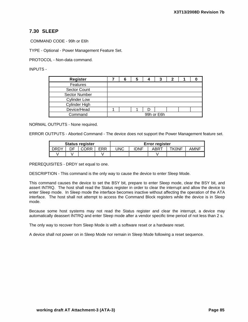
X3T13/2008D Revision 7b
working draft AT Attachment-3 (ATA-3) Page 85
7.30 SLEEP
COMMAND CODE - 99h or E6h
TYPE - Optional - Power Management Feature Set.
PROTOCOL - Non-data command.
INPUTS -
Register 7 6 5 4 3 2 1 0Features
Sector CountSector NumberCylinder LowCylinder HighDevice/Head 1 1 DCommand 99h or E6h
NORMAL OUTPUTS - None required.
ERROR OUTPUTS - Aborted Command - The device does not support the Power Management feature set.
Status register Error registerDRDY DF CORR ERR UNC IDNF ABRT TK0NF AMNF
V V V V
PREREQUISITES - DRDY set equal to one.
DESCRIPTION - This command is the only way to cause the device to enter Sleep Mode.
This command causes the device to set the BSY bit, prepare to enter Sleep mode, clear the BSY bit, andassert INTRQ. The host shall read the Status register in order to clear the interrupt and allow the device toenter Sleep mode. In Sleep mode the interface becomes inactive without affecting the operation of the ATAinterface. The host shall not attempt to access the Command Block registers while the device is in Sleepmode.
Because some host systems may not read the Status register and clear the interrupt, a device mayautomatically deassert INTRQ and enter Sleep mode after a vendor specific time period of not less than 2 s.
The only way to recover from Sleep Mode is with a software reset or a hardware reset.
A device shall not power on in Sleep Mode nor remain in Sleep Mode following a reset sequence.

X3T13/2008D Revision 7b
Page 86 working draft AT Attachment-3 (ATA-3)
7.31 SMART
7.31.1 SMART DISABLE OPERATIONS
COMMAND CODE - B0h
TYPE - Optional - SMART Feature set. If the SMART feature set is implemented, this command shall beimplemented.
PROTOCOL - Non-data command.
INPUTS - The Features register shall be set to D9h. The Cylinder Low register shall be set to 4Fh. TheCylinder High register shall be set to C2h.
Register 7 6 5 4 3 2 1 0Features D9h
Sector CountSector NumberCylinder Low 4FhCylinder High C2hDevice/Head 1 1 DCommand B0h
NORMAL OUTPUTS - None.
ERROR OUTPUTS - If the device does not support this command, if SMART is not enabled, or if the valuesin the Features, Cylinder Low or Cylinder High registers are invalid, an Aborted command error is posted.
Status register Error registerDRDY DF CORR ERR UNC IDNF ABRT TK0NF AMNF
V V V
PREREQUISITES - DRDY set equal to one. SMART enabled.
DESCRIPTION - This command disables all SMART capabilities within the device including any and all timerfunctions related exclusively to this feature. After receipt of this command the device will disable all SMARToperations. Attribute values will no longer be monitored or saved by the device. The state of SMART (eitherenabled or disabled) will be preserved by the device across power cycles.
Upon receipt of the SMART DISABLE OPERATIONS command from the host, the device sets BSY,disables SMART capabilities and functions, clears BSY, and asserts INTRQ.
After receipt of this command by the device, all other SMART commands, with the exception of SMARTENABLE OPERATIONS, are disabled and invalid and shall be aborted by the device (including SMARTDISABLE OPERATIONS commands), returning the Aborted command error.

X3T13/2008D Revision 7b
working draft AT Attachment-3 (ATA-3) Page 87
7.31.2 SMART ENABLE/DISABLE ATTRIBUTE AUTOSAVE
COMMAND CODE - B0h
TYPE - Optional - SMART Feature set. If the SMART feature set is implemented, this command shall beimplemented.
PROTOCOL - Non-data command.
INPUTS - The Features register shall be set to D2h. The Cylinder Low register shall be set to 4Fh. TheCylinder High register shall be set to C2h. The Sector Count register is set to 00h to disable attributeautosave and a value of F1h is set to enable attribute autosave.
Register 7 6 5 4 3 2 1 0Features D2h
Sector Count 00h or F1hSector NumberCylinder Low 4FhCylinder High C2hDevice/Head 1 1 DCommand B0h
NORMAL OUTPUTS - None.
ERROR OUTPUTS - If the device does not support this command, if SMART is disabled or if the values inthe Features, Cylinder Low or Cylinder High registers are invalid, an Aborted command error is posted.
Status register Error registerDRDY DF CORR ERR UNC IDNF ABRT TK0NF AMNF
V V V
PREREQUISITES - DRDY set equal to one. SMART enabled.
DESCRIPTION - This command enables and disables the optional attribute autosave feature of the device.Depending upon the implementation, this command may either allow the device, after some vendor specifiedevent, to automatically save its updated attribute values to non-volitile memory; or this command may causethe autosave feature to be disabled. The state of the attribute autosave feature (either enabled or disabled)will be preserved by the device across power cycles.
A value of zero written by the host into the device’s Sector Count register before issuing this command willcause this feature to be disabled. Disabling this feature does not preclude the device from saving attributevalues to non-volitile memory during some other normal operation such as during a power-on or power-offsequence or during an error recovery sequence.
A value of F1h written by the host into the device’s Sector Count register before issuing this command willcause this feature to be enabled. Any other meaning of this value or any other non-zero value written by thehost into this register before issuing this command is vendor specific. The meaning of any non-zero valuewritten to this register at this time will be preserved by the device across power cycles.
If the SMART ENABLE/DISABLE ATTRIBUTE AUTOSAVE command is supported by the device, uponreceipt of the command from the host, the device sets BSY, enables or disables the autosave feature(depending on the implementation), clears BSY, and asserts INTRQ.

X3T13/2008D Revision 7b
Page 88 working draft AT Attachment-3 (ATA-3)
If this command is not supported by the device, the device shall abort the command upon receipt from thehost, returning the Aborted command error.
During execution of the autosave routine the device shall not assert BSY nor deassert DRDY. If the devicereceives a command from the host while executing its autosave routine it must respond to the host withintwo seconds.

X3T13/2008D Revision 7b
working draft AT Attachment-3 (ATA-3) Page 89
7.31.3 SMART ENABLE OPERATIONS
COMMAND CODE - B0h
TYPE - Optional - SMART Feature set. If the SMART feature set is implemented, this command shall beimplemented.
PROTOCOL - Non-data command.
INPUTS - The Features register shall be set to D8h. The Cylinder Low register shall be set to 4Fh. TheCylinder High register shall be set to C2h.
Register 7 6 5 4 3 2 1 0Features D8h
Sector CountSector NumberCylinder Low 4FhCylinder High C2hDevice/Head 1 1 DCommand B0h
NORMAL OUTPUTS - None.
ERROR OUTPUTS - If the device does not support this command or if the values in the Features, CylinderLow, or Cylinder High registers are invalid, an Aborted command error is posted.
Status register Error registerDRDY DF CORR ERR UNC IDNF ABRT TK0NF AMNF
V V V
PREREQUISITES -DRDY set equal to one.
DESCRIPTION - This command enables access to all SMART capabilities within the device. Prior to receiptof this command attribute values are neither monitored nor saved by the device. The state of SMART (eitherenabled or disabled) will be preserved by the device across power cycles. Once enabled, the receipt ofsubsequent SMART ENABLE OPERATIONS commands shall not affect any of the attribute values.
Upon receipt of this command from the host, the device sets BSY, enables SMART capabilities andfunctions, clears BSY, and asserts INTRQ.

X3T13/2008D Revision 7b
Page 90 working draft AT Attachment-3 (ATA-3)
7.31.4 SMART READ ATTRIBUTE THRESHOLDS
COMMAND CODE - B0h
TYPE - Optional - SMART Feature set. If the SMART feature set is implemented, this command is optionaland not recommended.
PROTOCOL - PIO data in.
INPUTS - The Features register shall be set to D1h. The Cylinder Low register shall be set to 4Fh. TheCylinder High register shall be set to C2h.
Register 7 6 5 4 3 2 1 0Features D1h
Sector CountSector NumberCylinder Low 4FhCylinder High C2hDevice/Head 1 1 DCommand B0h
NORMAL OUTPUTS - None.
ERROR OUTPUTS - If the device does not support this command, if SMART disabled or if the values in theFeatures, Cylinder Low, or Cylinder High registers are invalid, an Aborted command error is posted.
Status register Error registerDRDY DF CORR ERR UNC IDNF ABRT TK0NF AMNF
V V V
PREREQUISITES - DRDY set equal to one. SMART enabled.
DESCRIPTION - This command returns the device’s attribute thresholds to the host. Upon receipt of thiscommand from the host, the device sets BSY, reads the attribute thresholds from non-volitile memory, setsDRQ, clears BSY, asserts INTRQ, and then waits for the host to transfer the 512 bytes of attribute thresholdinformation from the device via the Data register.
Table 17 defines the 512 bytes that make up the attribute threshold information. All multi-byte fields shown inthese data structures follow the byte ordering specified in 2.2.5.
The sequence of active attribute thresholds must appear in the same order as their corresponding attributevalues (see 7.31.5).
The data structure revision number shall be the same value used in the device attribute values datastructure.
Table 18 defines the 12 bytes that make up the information for each threshold entry in the device attributethresholds data structure. Attribute entries in the individual threshold data structure must be in the sameorder and correspond to the entries in the individual attribute data structure.
The attribute ID numbers are vendor specific. Any non-zero value in the attribute ID number indicates anactive attribute.
Attribute threshold values are to be set at the factory and are not changeable in the field.

X3T13/2008D Revision 7b
working draft AT Attachment-3 (ATA-3) Page 91
The data structure checksum is the two’s compliment of the result of a simple eight-bit addition of the first511 bytes in the data structure.
Table 17 −− Device attribute thresholds data structureDescription Bytes Format Type
Data structure revision number = 0x0004h for this revision 2 binary Rd only1st attribute threshold 12 ( Table 18) Rd only...............30th attribute threshold 12 ( Table 18) Rd onlyreserved (0x00) 18 Rd onlyVendor specific 131 Rd onlyData structure checksum 1 Rd only
Total bytes 512
Table 18 −− Individual threshold data structureDescription Bytes Format Type
Attribute ID number 1 binary Rd onlyAttribute threshold (for comparison with attribute values from0x00 to 0xFFh)
1 binary Rd only
0x00 “always passing” threshold value to be used for code test purposes 0x01 minimum value for normal operation 0xFD maximum value for normal operation 0xFE invalid for threshold value - not to be used 0xFF “always failing” threshold value to be used for code testpurposesReserved 10 Rd only
Total bytes 12

X3T13/2008D Revision 7b
Page 92 working draft AT Attachment-3 (ATA-3)
7.31.5 SMART READ ATTRIBUTE VALUES
COMMAND CODE - B0h
TYPE - Optional - SMART Feature set. If the SMART feature set is implemented, this command is optionaland not recommended.
PROTOCOL - PIO data in.
INPUTS - The Features register shall be set to D0h. The Cylinder Low register shall be set to 4Fh. TheCylinder High register shall be set to C2h.
Register 7 6 5 4 3 2 1 0Features D0h
Sector CountSector NumberCylinder Low 4FhCylinder High C2hDevice/Head 1 1 DCommand B0h
NORMAL OUTPUTS - None.
ERROR OUTPUTS - If the device does not support this command, if SMART is disabled or if the values inthe Features, Cylinder Low or Cylinder High registers are invalid, an Aborted command error is posted.
Status register Error registerDRDY DF CORR ERR UNC IDNF ABRT TK0NF AMNF
V V V
PREREQUISITES - DRDY set equal to one. SMART enabled.
DESCRIPTION - This command returns the device’s attribute values to the host. Upon receipt of thiscommand from the host, the device sets BSY, saves any updated attribute values to non-volitile memory,sets DRQ, clears BSY, asserts INTRQ, and then waits for the host to transfer the 512 bytes of attributevalue information from the device via the Data register.
Table 19 defines the 512 bytes that make up the attribute value information. All multi-byte fields shown inthese data structures follow the byte ordering described in 2.2.5.
The number of active attributes and, therefore, the number of active attribute values is determinedindependently by the device manufacturer for each individual device. All active attribute entries should beconcatenated together directly after the data structure revsion number. If there are fewer than thirty activeattributes implemented on a device, the excess locations in the data structure are reserved for futureattribute implementations and are designated as blanks containing the value 0x00h. Thus the first reservedbyte following the attribute entries shall be the 363rd byte in the structure, the first SMART capability byteshall be the 369th byte in the structure, etc.
The data structure revision number identifies which version of this data structure is implemented by a device.Upon initial release of this specification, the revision number will be set to 0x0004h. Later revisions, if any,will increment the revision number by one for each new revision. The revision number will be the same forboth the attribute value and attribute threshold structures.

X3T13/2008D Revision 7b
working draft AT Attachment-3 (ATA-3) Page 93
Table 20 defines the 12 bytes that make up the information for each attribute entry in the device attibutesdata stucture.
Table 19 −− Device attributes data structureDescription Bytes Format Type
Data structure revision number = 0x0004 for this specificationrevision
2 binary Rd only
1st device attribute 12 Table 20 Rd/Wrt ... ... ...30th device attribute 12 Table 20 Rd/Wrtreserved (0x00) 6 Rd onlySMART capability 2 Rd onlyreserved (0x00) 16 Rd/WrtVendor specific 125 Rd onlyData stucture checksum 1 Rd only
Total bytes 512
Table 20 −− Individual attribute data structureDescription Bytes Format Type
Attribute ID number (0x01 to 0xFFh) 1 binary Rd onlyStatus flags 2 bit flags Rd only Pre-failure/advisory bit Vendor specific (5 bits) reserved (10 bits)Attribute value (valid values from 0x01 to 0xFEh) 1 binary Rd only 0x00 invalid for attribute value - not to be used 0x01 minimum value 0x64 initial value for all attributes prior to any data collection 0xFD maximum value 0xFE value is not valid 0xFF invalid for attribute value - not to be usedVendor specific 8 binary Rd only
Total bytes 12
The attribute ID numbers and their definitions are vendor specific. Any non-zero value in the attribute IDnumber indicates an active attribute. Valid values for this byte are from 0x01 through 0xFFh.
Status flag
− Bit 0 -Pre-failure/advisory - If the value of this bit equals zero, an attribute value less than or equal toits corresponding attribute threshold indicates an advisory condition where the usage or age of thedevice has exceeded its intended design life period. If the value of this bit equals one, an atributevalue less than or equal to its corresponding attribute threshold indicates a pre-failure conditionwhere imminent loss of data is being predicted.
− Bit 1 Reserved for future use. − Bits 3 - 6 - Vendor specific.− Bits 7 - 15 - Reserved for future use.

X3T13/2008D Revision 7b
Page 94 working draft AT Attachment-3 (ATA-3)
Table 20 describes the range and meaning of the attribute values. Prior to the monitoring and saving ofattribute values, all values are set to 0x64h. The attribute values of 0x00h and 0xFFh are reserved andshould not be used by the device.
SMART capability
− Bit 0 - Pre-power mode attribute saving capability - If the value of this bit equals one, the device willsave its attribute values prior to going into a power saving mode (Idle, Standby, or Sleep modes).
− Bit 1 - Attribute autosave after event capability - If the value of this bit is equal to one, the device
supports the SMART ENABLE/DISABLE ATTRIBUTE AUTOSAVE comand. − Bits 2-15 - Reserved for future use.
The data structure checksum is the two’s compliment of the result of a simple eight-bit addition of the first511 bytes in the data structure.
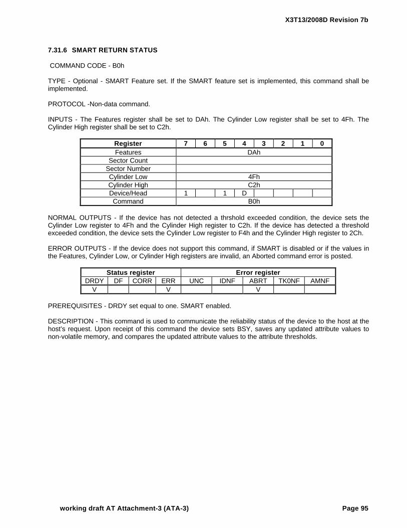
X3T13/2008D Revision 7b
working draft AT Attachment-3 (ATA-3) Page 95
7.31.6 SMART RETURN STATUS
COMMAND CODE - B0h
TYPE - Optional - SMART Feature set. If the SMART feature set is implemented, this command shall beimplemented.
PROTOCOL -Non-data command.
INPUTS - The Features register shall be set to DAh. The Cylinder Low register shall be set to 4Fh. TheCylinder High register shall be set to C2h.
Register 7 6 5 4 3 2 1 0Features DAh
Sector CountSector NumberCylinder Low 4FhCylinder High C2hDevice/Head 1 1 DCommand B0h
NORMAL OUTPUTS - If the device has not detected a thrshold exceeded condition, the device sets theCylinder Low register to 4Fh and the Cylinder High register to C2h. If the device has detected a thresholdexceeded condition, the device sets the Cylinder Low register to F4h and the Cylinder High register to 2Ch.
ERROR OUTPUTS - If the device does not support this command, if SMART is disabled or if the values inthe Features, Cylinder Low, or Cylinder High registers are invalid, an Aborted command error is posted.
Status register Error registerDRDY DF CORR ERR UNC IDNF ABRT TK0NF AMNF
V V V
PREREQUISITES - DRDY set equal to one. SMART enabled.
DESCRIPTION - This command is used to communicate the reliability status of the device to the host at thehost’s request. Upon receipt of this command the device sets BSY, saves any updated attribute values tonon-volatile memory, and compares the updated attribute values to the attribute thresholds.
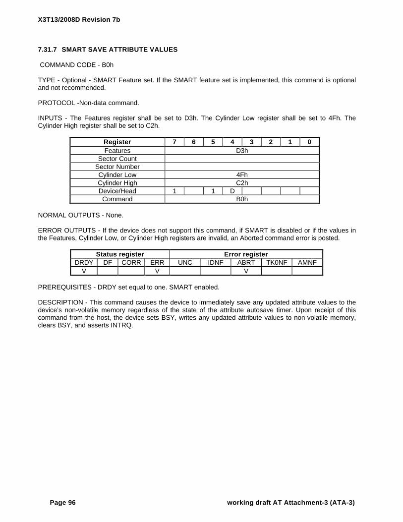
X3T13/2008D Revision 7b
Page 96 working draft AT Attachment-3 (ATA-3)
7.31.7 SMART SAVE ATTRIBUTE VALUES
COMMAND CODE - B0h
TYPE - Optional - SMART Feature set. If the SMART feature set is implemented, this command is optionaland not recommended.
PROTOCOL -Non-data command.
INPUTS - The Features register shall be set to D3h. The Cylinder Low register shall be set to 4Fh. TheCylinder High register shall be set to C2h.
Register 7 6 5 4 3 2 1 0Features D3h
Sector CountSector NumberCylinder Low 4FhCylinder High C2hDevice/Head 1 1 DCommand B0h
NORMAL OUTPUTS - None.
ERROR OUTPUTS - If the device does not support this command, if SMART is disabled or if the values inthe Features, Cylinder Low, or Cylinder High registers are invalid, an Aborted command error is posted.
Status register Error registerDRDY DF CORR ERR UNC IDNF ABRT TK0NF AMNF
V V V
PREREQUISITES - DRDY set equal to one. SMART enabled.
DESCRIPTION - This command causes the device to immediately save any updated attribute values to thedevice’s non-volatile memory regardless of the state of the attribute autosave timer. Upon receipt of thiscommand from the host, the device sets BSY, writes any updated attribute values to non-volatile memory,clears BSY, and asserts INTRQ.

X3T13/2008D Revision 7b
working draft AT Attachment-3 (ATA-3) Page 97
7.32 STANDBY
COMMAND CODE - 96h or E2h
TYPE - Optional - Power Management Feature Set.
PROTOCOL - Non-data command.
INPUTS - The value in the Sector Count register when the STANDBY command is issued shall determinethe time period programmed into the Standby Timer. Table 11 defines these values.
Register 7 6 5 4 3 2 1 0Features
Sector Count Time period valueSector NumberCylinder LowCylinder HighDevice/Head 1 1 DCommand 96h or E2h
NORMAL OUTPUTS - None required.
ERROR OUTPUTS - Aborted Command if the device does not support the Power Management feature set.
Status register Error registerDRDY DF CORR ERR UNC IDNF ABRT TK0NF AMNF
V V V V
PREREQUISITES - DRDY set equal to one.
DESCRIPTION - This command causes the device to set the BSY bit, enter the Standby Mode, clear theBSY bit, and assert INTRQ. INTRQ is asserted even though the device may not have fully transitioned toStandby Mode.
If the Sector Count register is non-zero then the Standby Timer shall be enabled. The value in the SectorCount register shall be used to determine the time programmed into the Standby Timer.
If the Sector Count register is zero then the Standby Timer is disabled.

X3T13/2008D Revision 7b
Page 98 working draft AT Attachment-3 (ATA-3)
7.33 STANDBY IMMEDIATE
COMMAND CODE - 94h or E0h
TYPE - Optional - Power Management Feature Set.
PROTOCOL - Non-data command.
INPUTS -
Register 7 6 5 4 3 2 1 0Features
Sector CountSector NumberCylinder LowCylinder HighDevice/Head 1 1 DCommand 94h or E0h
NORMAL OUTPUTS - None required.
ERROR OUTPUTS - Aborted Command - The device does not support the Power Management feature set.
Status register Error registerDRDY DF CORR ERR UNC IDNF ABRT TK0NF AMNF
V V V V
PREREQUISITES - DRDY set equal to one.
DESCRIPTION - This command causes the device to set the BSY bit, enter the Standby Mode, clear theBSY bit, and assert INTRQ. INTRQ is asserted even though the device may not have fully transitioned toStandby Mode.
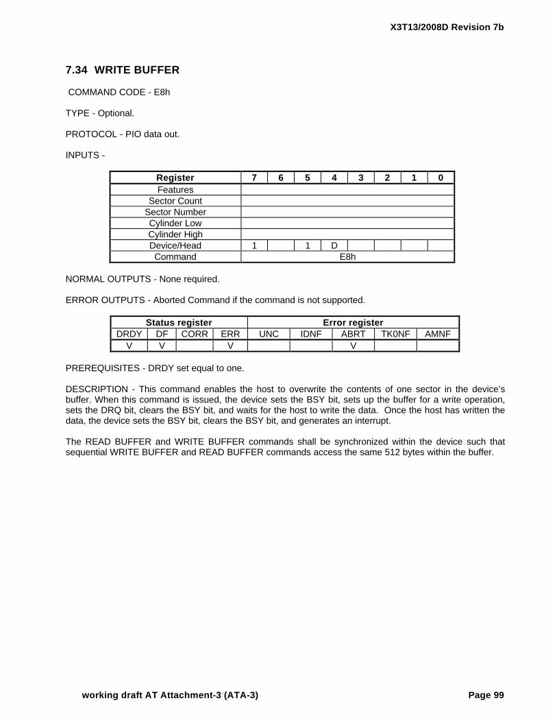
X3T13/2008D Revision 7b
working draft AT Attachment-3 (ATA-3) Page 99
7.34 WRITE BUFFER
COMMAND CODE - E8h
TYPE - Optional.
PROTOCOL - PIO data out.
INPUTS -
Register 7 6 5 4 3 2 1 0Features
Sector CountSector NumberCylinder LowCylinder HighDevice/Head 1 1 DCommand E8h
NORMAL OUTPUTS - None required.
ERROR OUTPUTS - Aborted Command if the command is not supported.
Status register Error registerDRDY DF CORR ERR UNC IDNF ABRT TK0NF AMNF
V V V V
PREREQUISITES - DRDY set equal to one.
DESCRIPTION - This command enables the host to overwrite the contents of one sector in the device’sbuffer. When this command is issued, the device sets the BSY bit, sets up the buffer for a write operation,sets the DRQ bit, clears the BSY bit, and waits for the host to write the data. Once the host has written thedata, the device sets the BSY bit, clears the BSY bit, and generates an interrupt.
The READ BUFFER and WRITE BUFFER commands shall be synchronized within the device such thatsequential WRITE BUFFER and READ BUFFER commands access the same 512 bytes within the buffer.

X3T13/2008D Revision 7b
Page 100 working draft AT Attachment-3 (ATA-3)
7.35 WRITE DMA (with retries and without retries)
COMMAND CODE - CAh (with retries) or CBh (without retries).
TYPE - Mandatory.
PROTOCOL - DMA.
INPUTS - The Cylinder Low, Cylinder High, Device/Head, and Sector Number specify the starting sectoraddress to be written. The Sector Count register specifies the number of sectors to be transferred.
Register 7 6 5 4 3 2 1 0Features
Sector Count Sector countSector Number Sector number or LBACylinder Low Cylinder low or LBACylinder High Cylinder high or LBADevice/Head 1 LBA 1 D Head number or LBACommand CAh or CBh
NORMAL OUTPUTS - None required.
ERROR OUTPUTS - An unrecoverable error encountered during the execution of this command results inthe termination of the command and the Command Block registers contain the sector address of the sectorwhere the first unrecoverable error occurred. The amount of data transferred is indeterminant.
Status register Error registerDRDY DF CORR ERR UNC IDNF ABRT TK0NF AMNF
V V V V V
PREREQUISITES - DRDY set equal to one. The host shall initialize the DMA channel.
DESCRIPTION - This command executes in a similar manner to WRITE SECTOR(S) except for thefollowing:
− the host initializes the DMA channel prior to issuing the command;− data transfers are qualified by DMARQ and are performed by the DMA channel;− the device issues only one interrupt per command to indicate that data transfer has terminated
and status is available.
During the execution of a WRITE DMA command, the device shall provide status of the BSY bit or the DRQbit until the command is completed.
Error recovery performed by the device either with or without retries is vendor specific.

X3T13/2008D Revision 7b
working draft AT Attachment-3 (ATA-3) Page 101
7.36 WRITE LONG (with retries and without retries)
COMMAND CODE - 32h (with retries) or 33h (without retries)
TYPE - Optional.
PROTOCOL - PIO data out.
INPUTS - The Cylinder Low, Cylinder High, Device/Head, and Sector Number specify the starting sectoraddress to be written. The Sector Count register shall not specify a value other than one.
Register 7 6 5 4 3 2 1 0Features
Sector Count 01hSector Number Sector number or LBACylinder Low Cylinder low or LBACylinder High Cylinder high or LBADevice/Head 1 LBA 1 D Head number or LBACommand 32h or 33h
NORMAL OUTPUTS - None required.
ERROR OUTPUTS - Aborted Command if the command is not supported. An unrecoverable errorencountered during the execution of this command results in the termination of the command and theCommand Block registers contain the sector address of the sector where the first unrecoverable erroroccurred. The amount of data transferred is indeterminant.
Status register Error registerDRDY DF CORR ERR UNC IDNF ABRT TK0NF AMNF
V V V V V
PREREQUISITES - The SET FEATURES subcommand to enable other than 4 vendor specific bytes shallbe executed prior to the WRITE LONG command if other than 4 vendor specific bytes are to be transferred.Additional prerequisites are vendor specific.
DESCRIPTION - This command is similar to the WRITE SECTOR(S) command except that it writes the dataand the vendor specific bytes as supplied by the host; the device does not generate the vendor specificbytes itself. Only single sector Write Long operations are supported.
The transfer of the vendor specific bytes shall be 16 bit transfers with the vendor specific byte in bits 7through 0. Bits 15 through 8 shall be ignored by the host.. The host shall use PIO mode 0 when using thiscommand.
Error recovery performed by the device either with or without retries is vendor specific.
NOTE − The committee is considering removing the READ LONG and WRITE LONGcommands in a future ATA standard.

X3T13/2008D Revision 7b
Page 102 working draft AT Attachment-3 (ATA-3)
7.37 WRITE MULTIPLE
COMMAND CODE - C5h
TYPE - Mandatory.
PROTOCOL - PIO data out.
INPUTS - The Cylinder Low, Cylinder High, Device/Head, and Sector Number specify the starting sectoraddress to be written. The Sector Count register specifies the number of sectors to be transferred.
Register 7 6 5 4 3 2 1 0Features
Sector Count Sector countSector Number Sector number or LBACylinder Low Cylinder low or LBACylinder High Cylinder high or LBADevice/Head 1 LBA 1 D Head number or LBACommand C5h
NORMAL OUTPUTS - None required.
ERROR OUTPUTS - An unrecoverable error encountered during the execution of this command results inthe termination of the command and the Command Block registers contain the sector address of the sectorwhere the first unrecoverable error occurred. The amount of data transferred is indeterminent.
Status register Error registerDRDY DF CORR ERR UNC IDNF ABRT TK0NF AMNF
V V V V V
PREREQUISITES - DRDY set equal to one. If bit 8 of Word 59 in the IDENTIFY DEVICE response is equalto zero, a successful SET MULTIPLE MODE command shall proceed a WRITE MULTIPLE command.
DESCRIPTION - This command is similar to the WRITE SECTOR(S) command. Interrupts are notgenerated on every sector, but on the transfer of a block that contains the number of sectors defined by SETMULTIPLE MODE or the default if no intervening SET MULTIPLE command has been issued.
Command execution is identical to the WRITE SECTOR(S) operation except that the number of sectorsdefined by the SET MULTIPLE MODE command are transferred without intervening interrupts. The DRQ bitqualification of the transfer is required only at the start of the data block, not on each sector.
The block count of sectors to be transferred without intervening interrupts is the default or programmed bythe SET MULTIPLE MODE command, which shall be executed prior to the WRITE MULTIPLE command.
When the WRITE MULTIPLE command is issued, the Sector Count register contains the number of sectors(not the number of blocks or the block count) requested.
If the number of requested sectors is not evenly divisible by the block count, as many full blocks as possibleare transferred, followed by a final, partial block transfer. The partial block transfer is for n sectors, where:
n = Remainder (sector count/ block count).
If the WRITE MULTIPLE command is attempted when WRITE MULTIPLE commands are disabled, theWrite Multiple operation shall be rejected with an Aborted Command error.

X3T13/2008D Revision 7b
working draft AT Attachment-3 (ATA-3) Page 103
Device errors encountered during WRITE MULTIPLE commands are posted after the attempted device writeof the block or partial block transferred. The Write command ends with the sector in error, even if it was inthe middle of a block. Subsequent blocks are not transferred in the event of an error.
The contents of the Command Block Registers following the transfer of a data block which had a sector inerror are undefined. The host should retry the transfer as individual requests to obtain valid errorinformation. Interrupts are generated when the DRQ bit is set at the beginning of each block or partial block.

X3T13/2008D Revision 7b
Page 104 working draft AT Attachment-3 (ATA-3)
7.38 WRITE SECTOR(S) (with retries and without retries)
COMMAND CODE - 30h (with retries) or 31h (without retries)
TYPE - Mandatory.
PROTOCOL - PIO data out.
INPUTS - The Cylinder Low, Cylinder High, Device/Head, and Sector Number specify the starting sectoraddress to be written. The Sector Count register specifies the number of sectors to be transferred.
Register 7 6 5 4 3 2 1 0Features
Sector Count Sector countSector Number Sector number or LBACylinder Low Cylinder low or LBACylinder High Cylinder high or LBADevice/Head 1 LBA 1 D Head number or LBACommand 30h or 31h
NORMAL OUTPUTS - None required.
ERROR OUTPUTS - An unrecoverable error encountered during the execution of this command results inthe termination of the command and the Command Block registers contain the sector address of the sectorwhere the first unrecoverable error occurred. The amount of data transferred is indeterminant.
Status register Error registerDRDY DF CORR ERR UNC IDNF ABRT TK0NF AMNF
V V V V V
PREREQUISITES - DRDY set equal to one.
DESCRIPTION - This command writes from 1 to 256 sectors as specified in the Sector Count register. Asector count of 0 requests 256 sectors.
The with retries and without retries versions of this command differ in operation only in the level of errorrecovery performed by the device. The level of error recovery performed by the device for either commandis vendor specific.

X3T13/2008D Revision 7b
working draft AT Attachment-3 (ATA-3) Page 105
7.39 WRITE VERIFY
COMMAND CODE - 3Ch
TYPE - Optional.
PROTOCOL - PIO data out.
INPUTS - The Cylinder Low, Cylinder High, Device/Head, and Sector Number specify the starting sectoraddress to be written. The Sector Count register specifies the number of sectors to be transferred.
Register 7 6 5 4 3 2 1 0Features
Sector Count Sector countSector Number Sector number or LBACylinder Low Cylinder low or LBACylinder High Cylinder high or LBADevice/Head 1 LBA 1 D Head number or LBACommand 3Ch
NORMAL OUTPUTS - None required.
ERROR OUTPUTS - Aborted Command if the command is not supported. An unrecoverable errorencountered during the execution of this command results in the termination of the command and theCommand Block registers contain the sector address of the sector where the first unrecoverable erroroccurred. The amount of data transferred is indeterminant.
Status register Error registerDRDY DF CORR ERR UNC IDNF ABRT TK0NF AMNF
V V V V V V V V
PREREQUISITES - DRDY set equal to one.
DESCRIPTION - This command is similar to the WRITE SECTOR(S) command, except that each sector isverified before the command is completed.

X3T13/2008D Revision 7b
Page 106 working draft AT Attachment-3 (ATA-3)
8 Protocol
Commands can be grouped into different classes according to the protocols followed for commandexecution. The command classes with their associated protocols are defined below.
For all commands, the host first checks if the BSY bit is equal to one, and should proceed no further unlessand until the BSY bit is equal to zero. For most commands, the host shall also wait for the DRDY bit to beequal to one before proceeding. The commands shown with DRDY=x can be executed when the DRDY bitis equal to zero.
Data transfers may be accomplished in more ways than are described below, but these sequences shouldwork with all known implementations of ATA devices.
A device shall maintain either the BSY bit equal to one or the DRQ bit equal to one at all times until thecommand is completed. The INTRQ signal is used by the device to signal most, but not all, times when theBSY bit is changed from one to zero during command execution.
A command shall only be interrupted with a hardware or software reset. The result of writing to theCommand register while the BSY bit is equal to one or the DRQ bit is equal to one is unpredictable and mayresult in data corruption.
8.1 Power on and hardware resets
This clause describes the algorithm and timing relationships for Devices 0 and 1 during the processing ofpower on and hardware resets.
The timing assumes the following:
a) DASP- is asserted by Device 1 and received by Device 0 at power-on or hardware reset toindicate the presence of Device 1. At all other times it is asserted by Device 0 or Device 1 toindicate when a device is active;
b) PDIAG- is asserted by Device 1 and detected by Device 0. It is used by Device 1 to indicate toDevice 0 that it has completed diagnostics without error and is ready to accept commands fromthe Host (BSY bit is cleared). This does not indicate that the device is ready, only that it canaccept commands.
8.1.1 Power on and hardware resets −− Device 0
a) Host asserts RESET- for a minimum of 25 µs;b) Device 0 sets the BSY bit no later than 400 ns after RESET- is negated;c) Device 0 negates DASP- no later than 1 ms after RESET- is negated;d) Device 0 samples for at least 450 ms for DASP- to be asserted from Device 1. This sampling
starts 1 ms after RESET- is negated;e) Device 0 performs hardware initialization and diagnostics;f) Device 0 may revert to its default condition;g) If Device 0 detected that DASP- was asserted during step (d), then Device 0 waits up to 31 s for
Device 1 to assert PDIAG-. Sampling of PDIAG- starts 1 ms after RESET is negated. If PDIAG-is asserted within 31 s, Device 0 clears bit 7 equal to zero in the Error Register, else Device 0sets bit 7 equal to one in the Error Register. If DASP- assertion was not detected in step (d)Device 0 clears bit 7 equal to zero in the Error Register. In either case the device shall set theSector Count register to 01h, the Sector Number register to 01h, the Cylinder Low register to00h, the Cylinder High register to 00h, and the Device/Head register to 00h. Device 0 shall storewhether or not Device 1 was detected in step (d) because this information is needed in order toprocess any Software reset or EXECUTE DEVICE DIAGNOSTIC command later;

X3T13/2008D Revision 7b
working draft AT Attachment-3 (ATA-3) Page 107
h) Device 0 posts diagnostic results to bits 6-0 of the Error Register;i) Device 0 clears the BSY bit when ready to accept commands that do not require the DRDY bit to
be equal to 1. Device 0 shall clear the BSY bit no later than 31 s from the time that RESET- isnegated;
j) Device 0 sets the DRDY bit when ready to accept any command.
NOTE − Steps (i) and (j) may occur at the same time. While no maximum time isspecified for the DRDY bit to be set to one, a host should allow up to 30 s for theDRDY bit to become 1. Figure 8 defines this timing.
8.1.2 Power on and hardware resets −− Device 1
a) Host asserts RESET- for a minimum of 25 µs;b) Device 1 sets the BSY bit no later than 400 ns after RESET- is negated;c) Device 1 negates DASP- no later than 1 ms after RESET- is negated;d) Device 1 negates PDIAG- before asserting DASP-;e) Device 1 asserts DASP- no later than 400 ms after RESET- is negated;f) Device 1 performs hardware initialization and diagnostics;g) Device 1 may revert to its default condition;h) Device 1 posts diagnostic results to the Error Register;i) Device 1 clears the BSY bit when ready to accept commands that do not require the DRDY bit to
be equal to 1;j) If Device 1 passed its diagnostics without error in step (f), Device 1 asserts PDIAG-. If thediagnostics failed, Device 1 does not assert PDIAG- and continues to the next step. Device 1 shallclear the BSY bit, and optionally assert PDIAG-, no later than 30 s from the time RESET- isnegated. The device shall set the Sector Count register to 01h, the Sector Number register to 01h,the Cylinder Low register to 00h, the Cylinder High register to 00h, and the Device/Head register to00h;k) Device 1 sets the DRDY bit when ready to accept any command;
NOTE − Steps (i), (j) and (k) may occur at the same time. While no maximum timeis specified for the DRDY bit to be set to one, a host should allow up to 30 s for theDRDY bit to become 1. Figure 8 defines this timing.
l) Device 1 negates DASP- after the first command is received or negates DASP- if no command isreceived within 31 s after RESET- is asserted.
RESET-
BSY
DRDY
Max for Device 0 Minimum time is is 31 s. 0 s. Max for Device 1 No maximum time is 30 s. is specified.
Figure 8 −− BSY and DRDY timing for power on and hardware resets
8.2 Software reset
This clause describes the algorithm and timing relationships for Devices 0 and 1 during the processing ofsoftware resets.
NOTE − Some devices may require SRST be set for a minimum of 5 µs.

X3T13/2008D Revision 7b
Page 108 working draft AT Attachment-3 (ATA-3)
8.2.1 Software reset −− Device 0
a) Host sets the SRST bit to one in the Device Control register;b) Device 0 sets BSY bit no later than 400 ns after detecting that the SRST bit is equal to one;c) Device 0 performs hardware initialization and diagnostics;d) Device 0 may revert to its default condition;e) Device 0 posts diagnostic results to the Error Register;f) Device 0 waits for the host to clear the SRST bit to zero;g) If Device 0 detected that Device 1 is present during the most recent power on or hardware reset
sequence, then Device 0 waits up to 31 s from the time that the SRST bit to become zero forDevice 1 to assert PDIAG-. Sampling of PDIAG- starts 1 ms after SRST is cleared to zero. IfPDIAG- is asserted within 31 s, Device 0 clears bit 7 equal to zero in the Error Register, elseDevice 0 sets bit 7 equal to one in the Error Register. If device 1 was not detected during themost recent power up or hardware reset sequence, then Device 0 clears bit 7 equal to zero inthe Error register. In either case the device shall set the Sector Count register to 01h, the SectorNumber register to 01h, the Cylinder Low register to 00h, the Cylinder High register to 00h, andthe Device/Head register to 00h;
h) Device 0 clears the BSY bit when ready to accept commands that do not require the DRDY bit tobe equal to 1. Device 0 shall clear the BSY bit no later than 31 s from the time that the hostclears the SRST bit equal to zero;
NOTE − Steps (g) and (h) may occur very rapidly.
i) Device 0 sets the DRDY bit when ready to accept any command.NOTE − Steps (h) and (i) may occur at the same time. While no maximum time isspecified for the DRDY bit to become equal to 1 to occur, a host should allow up to30 s for the DRDY bit to be set to one. Figure 9 defines this timing.
8.2.2 Software reset −− Device 1
a) Host sets SRST bit to one in the Device Control register;b) Device 1 set the BSY bit no later than 400 ns after detecting that the SRST bit to equal to one;c) Device 1 negates PDIAG- no later than 1 ms after detecting that the SRST bit is one;d) Device 1 perform hardware initialization and diagnostics;e) Device 1 may revert to its default condition;f) Device 1 posts diagnostic results to the Error Register;g) Device 1 waits for the host to clear the SRST bit equal to zero;h) Device 1 clears the BSY bit when ready to accept commands that do not require the DRDY bit to
be equal to 1;i) If Device 1 passed its diagnostics without error in step (d), Device 1 asserts PDIAG-. If the
diagnostics failed, Device 1 does not assert PDIAG- and continues to the next step. Device 1shall clear the BSY bit, optionally assert PDIAG-, no later than 30 s from the time the host clearsthe SRST bit to zero. The device shall set the Sector Count register to 01h, the Sector Numberregister to 01h, the Cylinder Low register to 00h, the Cylinder High register to 00h, and theDevice/Head register to 00h;
j) Device 1 sets the DRDY bit when ready to accept any command.NOTE − Steps (h), (i) and (j) may occur at the same time. While no maximum timeis specified for the DRDY bit to be set to one, a host should allow up to 30 s for theDRDY bit to become one. Figure 9 defines this timing.

X3T13/2008D Revision 7b
working draft AT Attachment-3 (ATA-3) Page 109
SRST
BSY
DRDY
Max for Device 0 Minimum time is is 31 s. 0 s. Max for Device 1 No maximum time is 30 s. is specified.
Figure 9 −− BSY and DRDY timing for software reset
8.3 PIO data in commands
This class includes:
− IDENTIFY DEVICE− READ BUFFER− READ LONG (with and without retry)− READ SECTOR(S) (with and without retry)− READ MULTIPLE− SMART READ ATTRIBUTE THRESHOLDS− SMART READ ATTRIBUTE VALUES
Execution of this class of command includes the transfer of one or more blocks of data from the device tothe host. Figure 10 describes the processing of a PIO data in command. This description does not include allpossible error conditions.

X3T13/2008D Revision 7b
Page 110 working draft AT Attachment-3 (ATA-3)
start
Host: Read the Status or Alternate Status register
No BSY=0?
Yes
Host: Write the Device/Head register with appropriate DEV bit value.
Host: Read the Status or Alternate Status register
BSY=0 & No DRDY=1?
Yes
Host: Write any required command parameters to the Features, Sector Count, Sector Number, Cylinder High, Cylinder Low and Device/Head registers.
Host: Writes the command code to the Command register.
Device: Set BSY and begin command execution.
Yes, B Error ? Device: Set error status, DRQ if desired No
Device: When data is available, set DRQ=1
Device: Set BSY=0
A
Figure 10 −− Example of PIO data transfer in diagram (continued)

X3T13/2008D Revision 7b
working draft AT Attachment-3 (ATA-3) Page 111
A
Interrupts Yes Device: enabled? Assert INTRQ
No
Host: Read Alternate Status register.
No BSY=0?
Yes
Host: Read and save Status register (Clears interrupt)
Device: Clear INTRQ
No DRQ=1 ?
Yes
Host: Transfer data from the device by performing a series of reads to the Data register
Error or no No more data?
Yes B
end
Figure 10 −− Example of PIO data transfer in diagram (concluded)

X3T13/2008D Revision 7b
Page 112 working draft AT Attachment-3 (ATA-3)
8.4 PIO data out commands
This class includes:
− DOWNLOAD MICROCODE− FORMAT TRACK− SECURITY DISABLE PASSWORD− SECURITY ERASE UNIT− SECURITY SET PASSWORD− SECURITY UNLOCK− WRITE BUFFER− WRITE LONG (with and without retry)− WRITE MULTIPLE− WRITE SECTOR(S) (with and without retry)− WRITE VERIFY
Execution of this class of command includes the transfer of one or more blocks of data from the host to thedevice. Figure 11 describes the processing of a PIO data out command.. This description does not includeall possible error conditions.

X3T13/2008D Revision 7b
working draft AT Attachment-3 (ATA-3) Page 113
start
Host: Read the Status or Alternate Status register
No BSY=0?
Yes
Host: Write the Device/Head register with appropriate DEV bit value.
Host: Read the Status or Alternate Status register
BSY=0 & No DRDY=1?
Yes
Host: Write any required command parameters to the Features, Sector Count, Sector Number, Cylinder High, Cylinder Low and Device/Head registers.
Host: Writes the command code to the Command register.
Device: Set BSY and begin command execution.
Yes, B Error ? Device: Set error status, DRQ if desired No
Device: When ready to receive data, set DRQ=1
Device: Set BSY=0
A
Figure 11 −− Example of PIO data transfer out diagram (continued)

X3T13/2008D Revision 7b
Page 114 working draft AT Attachment-3 (ATA-3)
A
No DRQ=1?
Yes
Host: Transfer data to device by performing a series of writes to the Data register.
Host: Read Status or Alternate Status register
Yes Error? Device: Set BSY & DRQ=0, assert INTRQ No
Device: Set BSY=1, process data from host end
Yes Error or transfer Device: Set BSY=0 complete and assert INTRQ No
Device: Set BSY=0 and DRQ=1
Interrupts Yes Device: Assert enabled? INTRQ
No
Host: Read Alternate Status register
No BSY=0?
Yes
Host: Read and save Status register (Clears interrupt)
B
Figure 11 −− Example of PIO data transfer out diagram (concluded)

X3T13/2008D Revision 7b
working draft AT Attachment-3 (ATA-3) Page 115
8.5 Non-data commands
This class includes:
− CHECK POWER MODE− DOOR LOCK− DOOR UNLOCK− EXECUTE DEVICE DIAGNOSTIC (DRDY=x)− IDLE− IDLE IMMEDIATE− INITIALIZE DEVICE PARAMETERS (DRDY=x)− MEDIA EJECT− NOP− READ VERIFY SECTOR(S)− RECALIBRATE− SECURITY ERASE PREPARE− SECURITY FREEZE LOCK− SEEK− SET FEATURES− SET MULTIPLE MODE− SLEEP− SMART DISABLE OPERATION− SMART ENABLE/DISABLE AUTOSAVE− SMART ENABLE OPERATION− SMART RETURN STATUS− SMART SAVE ATTRIBUTE VALUES− STANDBY− STANDBY IMMEDIATE
Execution of these commands involves no data transfer. Figure 12 describes the processing of a no datatransfer command. This description does not include all possible error conditions.
See the EXECUTE DEVICE DIAGNOSTICS command description in 7.5, the NOP command description in7.13 and the SLEEP command description in 7.30 for additional protocol requirements.

X3T13/2008D Revision 7b
Page 116 working draft AT Attachment-3 (ATA-3)
start
Host: Read the Status or Alternate Status register
No BSY=0?
Yes
Host: Write the Device/Head register with appropriate DEV bit value.
Host: Read the Status or Alternate Status register
BSY=0 & No DRDY=1?
Yes
Host: Write any required command parameters to the Features, Sector Count, Sector Number, Cylinder High, Cylinder Low and Device/Head registers.
Host: Writes the command code to the Command register.
Device: Set BSY and begin command execution.
Yes, Error ? Device: Set error status
No
Device: Set BSY=0
Interrupts No enabled?
Yes
Device: Assert INTRQ end
Figure 12 −− Example of non-data transfer diagram

X3T13/2008D Revision 7b
working draft AT Attachment-3 (ATA-3) Page 117
8.6 DMA data transfer commands
This class comprises:
− READ DMA (with and without retry)− WRITE DMA (with and without retry)− IDENTIFY DEVICE DMA
Data transfers using DMA commands differ in two ways from PIO transfers:
1) data transfers are performed using the DMA channel; 2) A Single interrupt is issued at the completion of the command.
Initiation of the DMA transfer commands is identical to the READ SECTOR(S) or WRITE SECTOR(S)commands except that the host initializes the DMA channel prior to issuing the command.
The interrupt handler for DMA transfers is different in that no intermediate sector interrupts are issued onmulti-sector commands.
Figure 13 describes the execution of a DMA command.

X3T13/2008D Revision 7b
Page 118 working draft AT Attachment-3 (ATA-3)
start
Host: Read the Status or Alternate Status register
No BSY=0?
Yes
Host: Write the Device/Head register with appropriate DEV bit value.
Host: Read the Status or Alternate Status register
BSY=0 & No DRDY=1?
Yes
Host: Write any required command parameters to the Features, Sector Count, Sector Number, Cylinder High, Cylinder Low and Device/Head registers.
Host: Initialize the DMA channel This action may occur at any point prior to this box.
Host: Write the command code to the Command register.
Device: Set BSY and begin command execution
Yes C Error? Device: Set error and status bits
No
Device: Assert DMARQ Yes Continue and transfer some data transfer?
No
A B
Figure 13 −− Example of DMA data transfer diagram (continued)

X3T13/2008D Revision 7b
working draft AT Attachment-3 (ATA-3) Page 119
A B
More No Device: Set BSY=0, DRQ=0, data? assert INTRQ, negate DMARQ
Yes
Device: Continue asserting Host: Disable DMA channel DRQ or BSY
C end
Figure 13 −− Example of DMA data transfer diagram (concluded)

X3T13/2008D Revision 7b
Page 120 working draft AT Attachment-3 (ATA-3)
8.7 Single device configurations
8.7.1 Device 0 only configurations
In a single device configuration where Device 0 is the only device and the host selects Device 1, Device 0may respond to accesses of the Command Block and Control Block registers in one of two methods. Thesetwo methods exist because previous versions of the ATA standard did not specify the required behavior forthis configuration. The first method is the recommended implementation.
The first method is:
a) A write to the Device Control register shall complete as if Device 0 was the selected device; b) A write to a Command Block register, other than the Command register, shall complete as if
Device 0 was selected; c) A write to the Command register is ignored; d) A read of the Control Block or Command Block registers, other than the Status or Alternate
Status registers, shall complete as if Device 0 was selected; e) A read of the Status or Alternate status register returns the value 00h;
NOTE − IDX is vendor specific and might change following reset or power modechanges resulting in values for status other than 00h.
The second method requires that Device 0 implement an Error, Status, and Alternate Status register that isused whenever Device 1 is selected.
The second method is:
a) The Device 1 Error, Status, and Alternate status registers are set to 00h by a reset;
NOTE − IDX is vendor specific and might change following reset or power mode changesresulting in values for status other than 00h;
b) A write to the Device Control register shall complete as if Device 0 was the selected device; c) A write to a Command Block register, other than the Command register, shall complete as if Device 0
was selected; d) A write to the Command register with a command code other than the INITIALIZE DEVICE
PARAMETERS or EXECUTE DEVICE DIAGNOSTICS command causes the Device 1 Error, Status,and Alternate Status registers to be used as follows:
1) the BSY bit is set in the Device 1 Status register; 2) the ABRT bit is set in the Device 1 Error register; 3) the ERR bit is set in the Device 1 Status register; 4) the BSY bit is cleared in the Device 1 Status register; 5) if the nIEN bit in the Device Control Register is cleared, the INTRQ signal is asserted.

X3T13/2008D Revision 7b
working draft AT Attachment-3 (ATA-3) Page 121
e) An EXECUTE DEVICE DIAGNOSTIC command is executed as if it addressed to Device 0;
f) An INITIALIZE DEVICE PARAMETERS command is executed as if Device 1 is present and is actually executing the command. The command shall have no effect of the device parameters of Device 0;
g) A read of the Control Block or Command Block registers, other than the Status or Alternate Status registers, shall complete as if Device 0 was selected;
h) A read of the Error, Status or Alternate status register returns the value in the device 1 copy of these registers. The Device 1 status registers shall contain 00h following a reset and the value 01h following an attempt to execute a command, other than EXECUTE DEVICE DIAGNOSTICS or INITIALIZE DEVICE PARAMETERS, on Device 1.
8.7.2 Device 1 only configurations
Host support of Device 1 only configurations is host specific.
In a single device configuration where Device 1 is the only device and the host selects Device 0, Device 1shall respond to accesses of the Command Block and Control Block registers in the same way it would ifDevice 0 was present. This is because Device 1 cannot determine if Device 0 is, or is not, present.
Host implementation of read and write operations to the Command and Control Block registers of non-existent Device 0 are host specific.
NOTE − The remainder of this section is a host implementation note.
The host implementor should be aware of the following when supporting Device 1 onlyconfigurations:
a) Following a hardware reset or software reset, Device 1 will not be selected. The followingsteps may be used to reselect Device 1:
1) Write to the Device/Head register with DRV bit set to one;
2) Using one or more of the Command Block registers that can be both written andread, such as the Sector Count or Sector Number, write a data pattern other than00h or FFh to the register(s);
3) Read the register(s) written in step (2). If the data read is the same as the datawritten, proceed to step (5);
4) Repeat steps (1) to (3) until the data matches in step (3) or until 31 s has past.After 31 s it can probably be assumed that Device 1 is not functioning properly;
5) Read the Status register and Error registers. Check the Status and Error registercontents for any error conditions that Device 1 may have posted.
b) Following the execution of an EXECUTE DEVICE DIAGNOSTICS command, Device 1will not be selected. Also, no interrupt will be generated to signal the completion of thecommand. After writing the EXECUTE DEVICE DIAGNOSTIC command to the Commandregister, execute steps (1) to (3) as described in (a) above;
c) At all other times, do not write zero into the DRV bit of the Device/Head register. All othercommands execute normally.

X3T13/2008D Revision 7b
Page 122 working draft AT Attachment-3 (ATA-3)
9 Timing
9.1 Deskewing
The host shall provide cable deskewing for all signals originating from the device. The device shall providecable deskewing for all signals originating at the host.
All timing values and diagrams are shown and measured at the connector of either device connected to theATA interface. No values are given for measurement at the host interface.
9.2 Symbols
Certain symbols are used in the timing diagrams. These symbols and their respective definitions are listedbelow.
or - signal transition (asserted or negated)
or - data transition (asserted or negated)
- undefined but not necessarily released
- the “other” condition if a signal is s hown with no change
All signals are shown with the asserted condition facing to the top of the page. The negated condition isshown towards the bottom of the page relative to the asserted condition.
9.3 Terms
The interface uses a mixture of negative and positive signals for control and data. The terms asserted andnegated are used for consistency and are independent of electrical characteristics.
In all timing diagrams, the lower line indicates negated, and the upper line indicates asserted e.g., thefollowing illustrates the representation of a signal named TEST going from negated to asserted and back tonegated, based on the polarity of the signal.
Assert Negate TEST Bit setting=1 Bit setting=0
Assert Negate TEST- Bit setting=0 Bit setting=1
9.4 Data transfers
The minimum cycle time supported by the device in PIO Mode 3, 4 and Multiword DMA Mode 1, 2respectively shall always be greater than or equal to the minimum cycle time defined by the associated Modee.g., a drive supporting PIO Mode 4 timing shall not report a value less than 120 ns, the minimum cycle timedefined for Mode 4 PIO Timings.

X3T13/2008D Revision 7b
working draft AT Attachment-3 (ATA-3) Page 123
9.4.1 Register transfers
Figure 14 defines the relationships between the interface signals for 8-bit PIO register transfers. This timingapplies to all register accesses except accesses to the Data register. Peripherals reporting support for PIOTransfer Mode 3 or 4 shall power up in a PIO Transfer Mode 0, 1 or 2.
For PIO modes 3 and above, the minimum value of t0 is specified by word 68 in the Identify Drive parameterlist. Table 21 defines the minimum value that shall be placed in word 68.
IORDY shall be supported when PIO Mode 3 or 4 are the current mode of operation.

X3T13/2008D Revision 7b
Page 124 working draft AT Attachment-3 (ATA-3)
t0
ADDR valid (See note 1) t1 t2 t9
t2i DIOR-/DIOW-
WRITE DD(7:0) (See note 2) t3 t4
READ DD(7:0) (See note 2) t5 t6
t6z
IORDY (See note 3,3-1) tA
IORDY (See note 3,3-2) tRD
IORDY (See note 3,3-3) tB
NOTES − 1 Device address consists of signals CS0-, CS1- and DA(2:0) 2 Data consists of DD(7:0). 3 The negation of IORDY by the device is used to extend the PIO cycle. The determination of whether the
cycle is to be extended is made by the host after tA from the assertion of DIOR- or DIOW-. Theassertion and negation of IORDY are described in the following three cases:3-1 Device never negates IORDY: no wait is generated.3-2 Device negates IORDY before tA, but causes IORDY to be asserted before tA: no wait generated.3-3 Device negates IORDY before tA: wait generated. The cycle completes after IORDY isreasserted. For cycles where a wait is generated and DIOR- is asserted, the device shall place readdata on DD(7:0) for tRD before asserting IORDY.
Figure 14 −− Register transfer to/from device
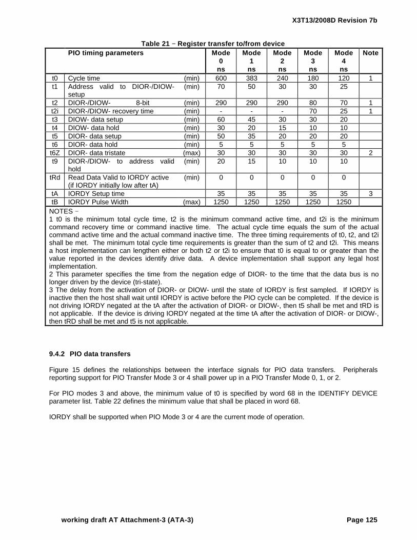
X3T13/2008D Revision 7b
working draft AT Attachment-3 (ATA-3) Page 125
Table 21 −− Register transfer to/from devicePIO timing parameters Mode
0ns
Mode1
ns
Mode2
ns
Mode3
ns
Mode4
ns
Note
t0 Cycle time (min) 600 383 240 180 120 1t1 Address valid to DIOR-/DIOW-
setup(min) 70 50 30 30 25
t2 DIOR-/DIOW- 8-bit (min) 290 290 290 80 70 1t2i DIOR-/DIOW- recovery time (min) - - - 70 25 1t3 DIOW- data setup (min) 60 45 30 30 20t4 DIOW- data hold (min) 30 20 15 10 10t5 DIOR- data setup (min) 50 35 20 20 20t6 DIOR- data hold (min) 5 5 5 5 5
t6Z DIOR- data tristate (max) 30 30 30 30 30 2t9 DIOR-/DIOW- to address valid
hold(min) 20 15 10 10 10
tRd Read Data Valid to IORDY active(if IORDY initially low after tA)
(min) 0 0 0 0 0
tA IORDY Setup time 35 35 35 35 35 3tB IORDY Pulse Width (max) 1250 1250 1250 1250 1250
NOTES −1 t0 is the minimum total cycle time, t2 is the minimum command active time, and t2i is the minimumcommand recovery time or command inactive time. The actual cycle time equals the sum of the actualcommand active time and the actual command inactive time. The three timing requirements of t0, t2, and t2ishall be met. The minimum total cycle time requirements is greater than the sum of t2 and t2i. This meansa host implementation can lengthen either or both t2 or t2i to ensure that t0 is equal to or greater than thevalue reported in the devices identify drive data. A device implementation shall support any legal hostimplementation.2 This parameter specifies the time from the negation edge of DIOR- to the time that the data bus is nolonger driven by the device (tri-state).3 The delay from the activation of DIOR- or DIOW- until the state of IORDY is first sampled. If IORDY isinactive then the host shall wait until IORDY is active before the PIO cycle can be completed. If the device isnot driving IORDY negated at the tA after the activation of DIOR- or DIOW-, then t5 shall be met and tRD isnot applicable. If the device is driving IORDY negated at the time tA after the activation of DIOR- or DIOW-,then tRD shall be met and t5 is not applicable.
9.4.2 PIO data transfers
Figure 15 defines the relationships between the interface signals for PIO data transfers. Peripheralsreporting support for PIO Transfer Mode 3 or 4 shall power up in a PIO Transfer Mode 0, 1, or 2.
For PIO modes 3 and above, the minimum value of t0 is specified by word 68 in the IDENTIFY DEVICEparameter list. Table 22 defines the minimum value that shall be placed in word 68.
IORDY shall be supported when PIO Mode 3 or 4 are the current mode of operation.

X3T13/2008D Revision 7b
Page 126 working draft AT Attachment-3 (ATA-3)
t0
ADDR valid (see note 1) t1 t2 t9
t2i
DIOR-/DIOW-
WRITE DD(15:0) (see note 2) t3 t4
READ DD(15:0) (see note 2) t5 t6
t6z
IORDY (see note 3,3-1) tA
IORDY (see note 3,3-2) tRD
IORDY (see note 3,3-3) tB
NOTES 1 Device address consists of signals CS0-, CS1- and DA(2:0) 2 Data consists of DD(15:0). For READ LONG and WRITE LONG commands, the transfer of the vendor
specific bytes shall be 16 bit transfers with the vendor specific byte in bits 7 through 0. Bits 15 through8 shall be ingnored.
3 The negation of IORDY by the device is used to extend the PIO cycle. The determination of whether thecycle is to be extended is made by the host after tA from the assertion of DIOR- or DIOW-. Theassertion and negation of IORDY are described in the following three cases:3-1 Device never negates IORDY: no wait is generated.3-2 Device negates IORDY before tA, but causes IORDY to be asserted before tA: no wait generated.3-3 Device negates IORDY before tA: wait generated. The cycle completes after IORDY isreasserted. For cycles where a wait is generated and DIOR- is asserted, the device shall place readdata on DD(15:0) for tRD before asserting IORDY.
Figure 15 −− PIO data transfer to/from device
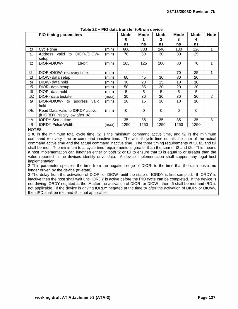
X3T13/2008D Revision 7b
working draft AT Attachment-3 (ATA-3) Page 127
Table 22 −− PIO data transfer to/from devicePIO timing parameters Mode
0ns
Mode1
ns
Mode2
ns
Mode3
ns
Mode4
ns
Note
t0 Cycle time (min) 600 383 240 180 120 1t1 Address valid to DIOR-/DIOW-
setup(min) 70 50 30 30 25
t2 DIOR-/DIOW- 16-bit (min) 165 125 100 80 70 1
t2i DIOR-/DIOW- recovery time (min) - - - 70 25 1t3 DIOW- data setup (min) 60 45 30 30 20t4 DIOW- data hold (min) 30 20 15 10 10t5 DIOR- data setup (min) 50 35 20 20 20t6 DIOR- data hold (min) 5 5 5 5 5
t6Z DIOR- data tristate (max) 30 30 30 30 30 2t9 DIOR-/DIOW- to address valid
hold(min) 20 15 10 10 10
tRd Read Data Valid to IORDY active(if IORDY initially low after tA)
(min) 0 0 0 0 0
tA IORDY Setup time 35 35 35 35 35 3tB IORDY Pulse Width (max) 1250 1250 1250 1250 1250
NOTES1 t0 is the minimum total cycle time, t2 is the minimum command active time, and t2i is the minimumcommand recovery time or command inactive time. The actual cycle time equals the sum of the actualcommand active time and the actual command inactive time. The three timing requirements of t0, t2, and t2ishall be met. The minimum total cycle time requirements is greater than the sum of t2 and t2i. This meansa host implementation can lengthen either or both t2 or t2i to ensure that t0 is equal to or greater than thevalue reported in the devices identify drive data. A device implementation shall support any legal hostimplementation.2 This parameter specifies the time from the negation edge of DIOR- to the time that the data bus is nolonger driven by the device (tri-state).3 The delay from the activation of DIOR- or DIOW- until the state of IORDY is first sampled. If IORDY isinactive then the host shall wait until IORDY is active before the PIO cycle can be completed. If the device isnot driving IORDY negated at the tA after the activation of DIOR- or DIOW-, then t5 shall be met and tRD isnot applicable. If the device is driving IORDY negated at the time tA after the activation of DIOR- or DIOW-,then tRD shall be met and t5 is not applicable.

X3T13/2008D Revision 7b
Page 128 working draft AT Attachment-3 (ATA-3)
9.4.3 Multiword DMA data transfer
Figure 16 defines the timings associated with Multiword DMA transfers.
For Multiword DMA modes 1 and above, the minimum value of t0 is specified by word 65 in the IDENTIFYDEVICE parameter list. Table 23 defines the minimum value that shall be placed in word 65.
Devices reporting support for Multiword DMA Transfer Mode 2 shall also support Multiword DMA TransferMode 0 and 1 and shall power up with Mode 0 as the default Multiword DMA Mode.
t0
DMARQ tL
DMACK- (see note) tI tD tK tJ
DIOR-/DIOW-
tE tZ Read DD(15:0)
tG tF Write DD(15:0)
tG tH
NOTE − This signal may be negated by the Host to suspend the DMA transfer in process. For Multi-Word DMA transfers, the Device may negate DMARQ within the tL specified time once DMACK- is asserted and reassert it again at a later time to resume the DMA operation. Alternatively, if the device is able to continue the transfer of data, the device may leave DMARQ asserted and wait for the host to reassert.
Figure 16 −− Multiword DMA data transfer

X3T13/2008D Revision 7b
working draft AT Attachment-3 (ATA-3) Page 129
Table 23 −− Multiword DMA data transferMultiword DMA timing parameters Mode 0
nsMode 1
nsMode 2
nsNote
t0 Cycle time (min) 480 150 120 see notetC DMACK to DMARQ delaytD DIOR-/DIOW- (min) 215 80 70 see notetE DIOR- data access (max) 150 60tF DIOR- data hold (min) 5 5 5tG DIOR-/DIOW- data setup (min) 100 30 20tH DIOW- data hold (min) 20 15 10tI DMACK to DIOR-/DIOW- setup (min) 0 0 0tJ DIOR-/DIOW- to DMACK hold (min) 20 5 5tKr DIOR- negated pulse width (min) 50 50 25 see notetKw DIOW- negated pulse width (min) 215 50 25 see notetLr DIOR- to DMARQ delay (max) 120 40 35tLw DIOW- to DMARQ delay (max) 40 40 35tZ DMACK- to tristate (max) 20 25 25
NOTE − t0 is the minimum total cycle time, tD is the minimum command active time, and tK (tKr or tKw, asappropriate) is the minimum command recovery time or command inactive time. The actual cycle timeequals the sum of the actual command active time and the actual command inactive time. The three timingrequirements of t0, tD, tK shall be met. The minimum total cycle time requirement, t0, is greater than thesum of tD and tK. This means a host implementation can lengthen either or both tD or tK to ensure that t0 isequal to the value reported in the devices identify drive data. A device implementation shall support anylegal host implementation.

X3T13/2008D Revision 7b
Page 130 working draft AT Attachment-3 (ATA-3)
Annex A(normative)
Connectors
A.1 40-pin connector
The I/O connector is a 40-pin connector as shown in figure A.1, with pin assignments as shown in table A.1.The connector shall be keyed to prevent the possibility of installing it upside down. A key is provided by theremoval of pin 20. The corresponding pin on the cable connector shall be plugged.
The pin locations are governed by the cable plug, not the receptacle. The way in which the receptacle ismounted on the printed circuit board affects the pin positions, and pin 1 shall remain in the same relativeposition. This means the pin numbers of the receptacle may not reflect the conductor number of the plug.The header receptacle is not polarized, and all the signals are relative to pin 20, which is keyed.
By using the plug positions as primary, a straight cable can connect devices. As shown in figure A.1,conductor 1 on pin 1 of the plug shall be in the same relative position no matter what the receptaclenumbering looks like. If receptacle numbering was followed, the cable would have to twist 180 degreesbetween a device with top-mounted receptacles, and a device with bottom-mounted receptacles.
140 20 2
Circuit board Circuit board1
40 20 2
Figure A.1 −− 40-pin connector mounting
Table A.1 −− 40-pin connector interface signalsSignal name Connector
contactConductor Connector
contactSignal name
RESET- 1 1 2 2 GroundDD7 3 3 4 4 DD8DD6 5 5 6 6 DD9DD5 7 7 8 8 DD10DD4 9 9 10 10 DD11DD3 11 11 12 12 DD12DD2 13 13 14 14 DD13DD1 15 15 16 16 DD14DD0 17 17 18 18 DD15
Ground 19 19 20 20 (keypin)DMARQ 21 21 22 22 GroundDIOW- 23 23 24 24 GroundDIOR- 25 25 26 26 GroundIORDY 27 27 28 28 CSEL
DMACK- 29 29 30 30 GroundINTRQ 31 31 32 32 reserved
DA1 33 33 34 34 PDIAG-DA0 35 35 36 36 DA2CS0- 37 37 38 38 CS1-
DASP- 39 39 40 40 Ground

X3T13/2008D Revision 7b
working draft AT Attachment-3 (ATA-3) Page 131
Recommended part numbers for the mating connector and cable are shown below, but equivalent parts maybe used.
Connector (40 pin) : 3M 3417-7000 or equivalentStrain relief : 3M 3448-2040 or equivalent
Flat cable (stranded 28 AWG) : 3M 3365-40 or equivalentFlat cable (stranded 28 AWG) : 3M 3517-40 (shielded) or equivalent
A.1.1 4-pin power connector
When the device uses the 40-pin connector, the device receives DC power through a 4-pin connector. Thepin assignments are shown in table A.2 and the connector pin locations are shown if figure A.2.Recommended part numbers for the mating connector to 18 AWG cable are shown below, but compatibleparts may be used.
Connector (4 pin) : AMP 1-480424-0 or compatibleContacts (loose piece) : AMP 60619-4 or compatibleContacts (strip) : AMP 61117-4 or compatible
Table A.2 −− DC interface using 4-pin power connectorPower line designation Pin Number
+12 Volts 1+12 Volt return 2+5 Volt return 3
+5 Volts 4
4 3 2 1 +5 V DC +5 V return +12 V return +12 V DC
Figure A.2 −− Drive side connector pin numbering
A.2 44-pin small form factor connector
This annex describes a connector alternative often used for 2 1/2 inch or smaller devices. This alternativewas developed by the Small Form Factor (SFF) Committee, an industry ad hoc group.
In an effort to broaden the applications for small form factor devices, a group of companies representingsystem integrators, device suppliers, and component suppliers decided to address the issues involved.
A primary purpose of the SFF Committee was to define the external dimensions of small form factor devicesso that products from different vendors could be used in the same mounting configurations.
The restricted area and the mating of devices directly to a motherboard required that the number ofconnectors be reduced, which caused the assignment of additional pins for power. Power is provided to thedevices on the same connector as used for the signals, and addresses are set by the receptacle into whichthe devices are plugged.
The 50-pin connector that has been widely adopted across industry for SFF devices is a low density 2 mmconnector which has no shroud on the plug which is mounted on the device. A number of suppliers provide

X3T13/2008D Revision 7b
Page 132 working draft AT Attachment-3 (ATA-3)
intermatable components. The following information has been provided to assist users in specifyingcomponents used in an implementation.
Signals Connector Plug : DuPont 86451 or equivalentSignals Connector Receptacle : DuPont 86455 or equivalent
A.2.1 44-pin signal assignments
The signals assigned for 44-pin applications are described in table A.3. Although there are 50 pins in theplug, a 44-pin mating receptacle may be used (the removal of pins E and F provides room for the wall of thereceptacle).
Some devices may utilize pins A, B, C, and D for option selection via physical jumpers. Suchimplementations may require use of the 44-pin receptacle.
The first four pins of the connector plug located on the device shall not to be connected to the host, as theyare reserved for manufacturer's use. Pins E, F, and 20 are keys, and are removed (see figure A.3).
43
19 1 E C A
KK K
44
20
2 F D B
Figure A.3 −− 44-pin connector

X3T13/2008D Revision 7b
working draft AT Attachment-3 (ATA-3) Page 133
Table A.3 −− Signal assignments for 44-pin ATASignal name Connector
contactConductor Connector
contactSignal name
Vendor specific A B Vendor specificVendor specific C D Vendor specific
(keypin) E F (keypin)RESET- 1 1 2 2 Ground
DD7 3 3 4 4 DD8DD6 5 5 6 6 DD9DD5 7 7 8 8 DD10DD4 9 9 10 10 DD11DD3 11 11 12 12 DD12DD2 13 13 14 14 DD13DD1 15 15 16 16 DD14DD0 17 17 18 18 DD15
Ground 19 19 20 20 (keypin)DMARQ 21 21 22 22 GroundDIOW- 23 23 24 24 GroundDIOR- 25 25 26 26 GroundIORDY 27 27 28 28 CSEL
DMACK- 29 29 30 30 GroundINTRQ 31 31 32 32 reserved
DA1 33 33 34 34 PDIAG-DA0 35 35 36 36 DA2CS0- 37 37 38 38 CS1-
DASP- 39 39 40 40 Ground+5 V (logic)(see note)
41 41 42 42 +5 V (Motor)(see note)
Ground(return)(see note)
43 43 44 44 TYPE- (0=ATA)(see note)
NOTE − Pins which are additional to those of the 40-pin cable.

X3T13/2008D Revision 7b
Page 134 working draft AT Attachment-3 (ATA-3)
A.3 68-pin small form factor connector
This clause defines the pinouts used for the 68-pin alternative connector for the AT Attachment Interface.This connector is the same as the one defined by PCMCIA. This clause defines a pinout alternative thatallows a device to function as an AT Attachment Interface compliant device, while also allowing the device tobe compliant with PC Card ATA mode defined by PCMCIA. The signal protocol allows the device to identifythe host interface as being 68-pin ATA or PC Card ATA.
To simplify the implementation of dual-interface devices, the 68-pin AT Attachment Interface maintainscommonality with as many PC Card ATA signals as possible, while supporting full command and signalcompliance with the ATA standard.
The 68-pin ATA pinout shall not cause damage or loss of data if a PCMCIA card is accidentally plugged intoa host slot supporting this interface. The inversion of the reset signal between the ATA and PCMCIAinterfaces prevents loss of data if the device is unable to reconfigure itself to the appropriate host interface.
A.3.1 Signals
This specification relies upon the electrical and mechanical characteristics of PCMCIA and unless otherwisenoted, all signals and registers with the same names as PCMCIA signals and registers have the samemeaning as defined in PCMCIA.
The PC Card-ATA specification is used as a reference to identify the signal protocol used to identify the hostinterface protocol.
A.3.2 Signal descriptions
Any signals not defined below shall be as described in the ATA, PCMCIA, or the PC Card ATA documents.
Table A.4 shows the ATA signals and relationships such as direction, as well as providing the signal name ofthe PCMCIA equivalent.

X3T13/2008D Revision 7b
working draft AT Attachment-3 (ATA-3) Page 135
Table A.4 −− Signal assignments for 68-pin ATAPin Signal Hst Dir Dev PCMCI
APin Signal Hst Dir Dev PCMCIA
1 Ground x → x Ground 35 Ground x → x Ground2 DD3 x ↔ x D3 36 CD1- x ← x CD1-3 DD4 x ↔ x D4 37 DD11 x ↔ x D114 DD5 x ↔ x D5 38 DD12 x ↔ x D125 DD6 x ↔ x D6 39 DD13 x ↔ x D136 DD7 x ↔ x D7 40 DD14 x ↔ x D147 CS0- x → x CE1- 41 DD15 x ↔ x D158 → i A10 42 CS1- x → x(1) CE2-9 SELATA- x → x OE- 43 ← i VS1-10 44 DIOR- x → x IORD-11 CS1- x → x(1) A9 45 DIOW- x → x IOWR-12 → i A8 4613 4714 4815 → i WE- 4916 INTRQ x ← x READY/
IREQ-50
17 Vcc x → x Vcc 51 Vcc x → x Vcc18 5219 5320 5421 55 M/S- x → x(2)22 → i A7 56 CSEL x → x(2)23 → i A6 57 ← i VS2-24 → i A5 58 RESET- x → x RESET25 → i A4 59 IORDY o ← x(3) WAIT-26 → i A3 60 DMARQ o ← x(3) INPACK-27 DA2 x → x A2 61 DMACK- o → o REG-28 DA1 x → x A1 62 DASP- x ↔ x BVD2/
SPKR-29 DA0 x → x A0 63 PDIAG- x ↔ x BVD1/
STSCHG30 DD0 x ↔ x D0 64 DD8 x ↔ x D831 DD1 x ↔ x D1 65 DD9 x ↔ x D932 DD2 x ↔ x D2 66 DD10 x ↔ x D1033 x ← x WP/
IOIS1667 CD2- x ← x CD2-
34 Ground x → x Ground 68 Ground x → x GroundKey:Dir = the direction of the signal between host and device.x in the Hst column = this signal shall be supported by the Host.x in the Dev column = this signal shall be supported by the device.i in the Dev column = this signal shall be ignored by the device while in 68-pin ATA mode.o = this signal is Optional.Nothing in Dev column = no connection should be made to that pin.
NOTES −−1 The device shall support only one CS1- signal pin.2 The device shall support either M/S- or CSEL but not both.3 The device shall hold this signal negated if it does not support the function.

X3T13/2008D Revision 7b
Page 136 working draft AT Attachment-3 (ATA-3)
A.3.2.1 CD1- (Card Detect 1)
This signal shall be grounded by the device. CD1- and CD2- are used by the host to detect the presence ofthe device.
A.3.2.2 CD2- (Card Detect 2)
This signal shall be grounded by the device. CD1- and CD2- are used by the host to detect the presence ofthe device.
A.3.2.3 CS1- (Device chip select 1)
Hosts shall provide CS1- on both the pins identified in table A.4.
Devices shall recognize only one of the two pins as CS1-.
A.3.2.4 DMACK- (DMA acknowledge)
This signal is optional for hosts and devices.
If this signal is supported by the host or the device, the function of DMARQ shall also be supported.
A.3.2.5 DMARQ (DMA request)
This signal is optional for hosts.
If this signal is supported by the host or the device, the function of DMACK- shall also be supported.
A.3.2.6 IORDY (I/O channel ready)
This signal is optional for hosts.
A.3.2.7 M/S- (Master/slave)
This signal is the inverted form of CSEL. Hosts shall support both M/S- and CSEL though devices need onlysupport one or the other.
Hosts shall assert CSEL and M/S- prior to applying VCC to the connector.
A.3.2.8 SELATA- (Select 68-pin ATA)
This pin is used by the host to select which mode to use, PC Card-ATA mode or the 68-pin ATA mode. Toselect 68-pin ATA mode, the host shall assert SELATA- prior to applying power to the connector, and shallhold SELATA- asserted.
The device shall not re-sample SELATA- as a result of either a Hard or Soft Reset. The device shall ignoreall interface signals for 19 ms after the host supplies Vcc within the device's voltage tolerance. If SELATA- isnegated following this time, the device shall either configure itself for PC Card-ATA mode or not respond tofurther inputs from the host.
A.3.3 Removability considerations
This specification supports the removability of devices which use the ATA protocol. As removability is a newconsideration for ATA devices, several issues need to be considered with regard to the insertion or removalof devices.

X3T13/2008D Revision 7b
working draft AT Attachment-3 (ATA-3) Page 137
A.3.3.1 Device recommendations
The following are recommendations to device implementors:
− CS0-, CS1-, RESET-, and SELATA- signals be negated on the device to prevent false selectionduring hot insertion.
− Ignore all interface signals except SELATA- until 19 ms after the host supplies VCC within the
device's voltage tolerance. This time is necessary to de-bounce the device's power on resetsequence. Once in the 68-pin ATA mode, if SELATA- is ever negated following the 19 ms de-bounce delay time, the device disables itself until VCC is removed.
− The DOOR LOCK and DOOR UNLOCK commands and the MC and MCR bits in the Error
register are used to prevent unexpected removal of the device or media.
A.3.3.2 Host recommendations
The following are recommendations to host implementors:
− Connector pin sequencing to protect the device by making contact to ground before any othersignal in the system.
− SELATA- to be asserted at all times. − All devices reset and reconfigured to the same base address each time a device at that address
is inserted or removed. − The removal or insertion of a device at the same address to be detected so as to prevent the
corruption of a command. − The DOOR LOCK and DOOR UNLOCK commands and the MC and MCR bits in the Error
register used to prevent unexpected removal of the device or media.

X3T13/2008D Revision 7b
Page 138 working draft AT Attachment-3 (ATA-3)
Annex B(informative)
Identify device data for ATA devices below 8 GB
B.1 Definitions and background information
The following abbreviations are used in this annex:
− 528 MB is used to describe a device that has 1,032,192 sectors or 528,482,304 bytes.− 8 GB is used to describe a device that has 16,515,072 sectors or 8,455,716,864 bytes.
The original IBM PC BIOS (Basic Input/Output System) imposed several restrictions on the support ofdevices, and these have been incorporated into many higher level software products. One such restrictionlimits the capacity of a device. Most BIOS software cannot support a device with more than 1,024 cylinders,16 heads and 63 sectors per track. The maximum addressable capacity of a device under this scheme is528 MB.
There is growing support of auto-configuration for devices on PC systems. The auto-configuration capabilityusually resides in the BIOS and uses the IDENTIFY DEVICE command data to configure a device.
This annex defines rules for the IDENTIFY DEVICE data of all capacity devices and allows BIOS support ofdevices up to 8 GB using Cylinder/Head/Sector (CHS) addressing.
This specification defines information that newer BIOSs and system software can use to determine the truesize of a device and access the full capacity of the device.
B.2 Cylinder, head, and sector addressing
BIOSs and other software that operate a device in CHS (Cylinder, Head, and Sector) addressing mode useIDENTIFY DEVICE data words 1, 3, 6, and words 53-58 to ascertain the appropriate translation mode to useand determine the capacity of a device.
Maximum compatibility is achieved if the following rules are obeyed. These rules limit the values placed intowords 1, 3, 6, and 53-58. The rules specified here for CHS addressing apply to devices up to 8 GB.
B.2.1 Word 1
For devices less than or equal to 528 MB, IDENTIFY DEVICE data word 1 (Default Cylinders) does notspecify a value greater than 1,024.
If a device is greater than 528 MB but less than or equal to 8 GB, the maximum value that is placed into thisword is determined by the value in Word 3 as shown in table B.1.
NOTE − This algorithm reserves a gap at cylinder address 16,384 to support the legacy of amaintenance cylinder.

X3T13/2008D Revision 7b
working draft AT Attachment-3 (ATA-3) Page 139
Table B.1 −− Word 1 valueValue in Word 3 Maximum value in Word 1
1 1h 65,535 FFFFh2 2h 65,535 FFFFh3 3h 65,535 FFFFh4 4h 65,535 FFFFh5 5h 32,767 7FFFh6 6h 32,767 7FFFh7 7h 32,767 7FFFh8 8h 32,767 7FFFh9 9h 16,383 3FFFh
10 Ah 16,383 3FFFh11 Bh 16,383 3FFFh12 Ch 16,383 3FFFh13 Dh 16,383 3FFFh14 Eh 16,383 3FFFh15 Fh 16,383 3FFFh16 10h 16,383 3FFFh
The value in this word does not change.
B.2.2 Word 3
IDENTIFY DEVICE data word 3 (Default Heads) does not specify a value greater than 16.
The value in this word does not change.
B.2.3 Word 6
For devices of 8 GB or less, IDENTIFY DEVICE data word 6 (Default Sectors) does not specify a valuegreater than 63.
The value in this word does not change.
B.2.4 Use of words 53 through 58
Devices that are over 528 MB implement words 53-58. Devices not over 528 MB may also implement thesewords. These words define the addressing for all sectors accessible in CHS mode.
B.2.5 Word 53
IDENTIFY DEVICE data word 53 bit 0 is set to one at all times that the device is in a valid translation mode.Some devices may have translation modes that cannot be supported. An attempt to put a device into one ofthese unsupported modes causes word 53 bit 0 to be cleared to zero with words 54-58 cleared to zero until avalid translation mode is established.
B.2.6 Word 54
IDENTIFY DEVICE data word 54 (Current Cylinders) specifies the number of full logical cylinders that can beaccessed in the current translation mode. If an INITIALIZE DEVICE PARAMETERS command has not beenexecuted, the contents of this word is the same as word 1. If an INITIALIZE DEVICE PARAMETERScommand has been executed, this word is the integer result of dividing the total number of user sectors (thisvalue may be in words 60-61) by the number of sectors per logical cylinder ( [word55] x [word56] ), but is nota value greater than 65,535.
X3T13/2008D Revision 7b
Page 140 working draft AT Attachment-3 (ATA-3)
B.2.7 Word 55
IDENTIFY DEVICE data word 55 (Current Heads) is the number of heads specified by the last INITIALIZEDEVICE PARAMETERS command. This word contains a value of between 1 and 16. If an INITIALIZEDEVICE PARAMETERS command has not been executed, the contents of this word are the same as word3.
B.2.8 Word 56
IDENTIFY DEVICE data word 56 (Current Sectors) is the number of sectors specified by the last INITIALIZEDEVICE PARAMETERS command. This word may contain a value of between 1 and 255. If an INITIALIZEDEVICE PARAMETERS command has not been executed, the contents of this word are the same as word6.
B.2.9 Words 57-58
IDENTIFY DEVICE data words 57-58 contain a 32-bit value that is equal to [word54] x [word55] x [word56].Words 57-58 are less than or equal to the value in words 60-61 at all times.
B.3 Orphan sectors
The sectors, if any, between the last sector addressable in CHS mode and the last sector addressable inLBA mode are known as "orphan" sectors. A device may or may not allow access to these sectors in CHSaddressing mode.
The values in words 1, 3, and 6 are selected such that the number of orphan sectors is minimized.Normally, the number of orphan sectors should not exceed ( [word55] x [word56] - 1 ). However, the hostsystem can create conditions where there are a larger number of orphans sectors by issuing the INITIALIZEDEVICE PARAMETERS command with values other than the values in words 3 and 6.

X3T13/2008D Revision 7b
working draft AT Attachment-3 (ATA-3) Page 141
Annex C(informative)
Signal integrity
C.1 Introduction
The ATA Bus (a.k.a. IDE bus) is a disk drive interface originally designed for the ISA Bus of the IBMPC/AT. With the advent of faster disk drives the definition of the ATA Bus has been expanded to includenew operating modes. Each of the PIO modes, numbered zero through four, is faster than the one before it(higher numbers translate to faster transfer rates). Modes 0, 1, and 2 correspond to the ATA interface asoriginally defined. PIO Mode 3 defines a maximum transfer rate of 11.1 MB/s and PIO Mode 4 defines amaximum rate of 16.7 MB/s. Additional DMA modes have also been defined, with Multiword DMA Mode 0corresponding to the original interface, and DMA Modes 1 and 2 being faster transfer rates. Multiword DMAMode 2 is the same speed as the new PIO Mode 4.
With this increased speed, the weaknesses of the original ATA cabling scheme have become apparent ondesktop systems. System manufacturers, chipset designers, and disk drive manufacturers must all takemeasures to insure that signal integrity is maintained on the bus. The areas of concern are:
a) ringing due to improper termination;b) crosstalk between signals;c) bus timing.
The intended audience for this annex is digital and analog engineers who design circuits interfacing to theATA bus. Familiarity with the ATA specification and a basic understanding of circuit theory is assumed.
C.1.1 The problems
Early implementations of the ATA bus used LS-TTL parts to drive an 18-inch cable. The slow edges of LS-TTL and the short cable length worked well at the time. PIO Modes 3 and 4 demand higher performance. Inan effort to cut cycle times, edge rates have inadvertently been increased, causing ringing on the cable andincreased crosstalk between adjacent signals.
When an ATA host adapter was little more than a few buffers and some gates there was no issue with hostadapter timing. With the advent of local bus architectures and faster transfer rates, timing issues havebecome more important. Propagation delay with worst-case loads must now be taken into account whendesigning host adapters.
One of the frequently asked questions is why are problems with ringing on the ATA bus seen now when theywere not seen before. The answer is in the edge speed of the logic. How the edge speed changed can befound by looking at the history of the IBM PC.
When the IBM PC/AT was introduced in 1983, the 8 MHz 80286 processor quickly became the dominantplatform. The AT bus (now called the ISA bus) became standardized around an 8 MHz processor speed.When the first ATA disk drive was introduced a few years later, it was designed as a simple extension of thebus – hence the name “AT Attachment” interface (see figure C.1). The idea was to remove the disk drivecontroller electronics from the PC and place them on the drive instead. What remained on the PC was a pairof bidirectional data buffers and an address decoder. This simple interface was most often implemented witha pair of 74LS245 buffers and a programmable logic device such as a PAL. These TTL devices had rise andfall times in the 5 to 6 ns range. Although this was fast enough to cause some ringing on the ATA bus, it wasnot so severe as to prevent millions of successful system implementations.

X3T13/2008D Revision 7b
Page 142 working draft AT Attachment-3 (ATA-3)
CPU Bus ISA Bus ATA Intf Device 8 Mhz Interface 8 Mhz (simple)
RAM Card Slots
ROM
Figure C.1 −− Original IBM PC/AT architecture
The architecture of modern PCs has changed somewhat from the original PC/AT. As the processor speedincreased it became necessary to separate the processor bus from the ISA bus (see figure C.2). To maintaincompatibility the ISA bus continues to run at an 8 MHz rate. Processors, and their associated busses, haveincreased from 8 MHz to 12, 16, 25, and now 33 Mhz.
NOTE − Processors that run faster than 33 MHz, such as the 486DX2-66, still tend to keepthe external processor bus at 33 MHz.
Disk drives have also increased in speed. The increase in rotational speed and linear bit density hasincreased the rate at which data comes off the heads, and the presence of cache on the drive makes dataavailable at the access rates of RAM. This has created a data bottleneck at the ISA bus. The drive is faster,the processor is faster, but the data can’t be moved from one to the other any faster.
CPU Bus ISA Bus 33 Mhz Interface 8 Mhz Card Slots RAM
ROM Local Bus Local Bus ATA Intf ATA Device Interface 33 MHz (complex) (fast)
Local Bus Card Slots
Figure C.2 −− Modern PC architecture
This bottleneck inspired the invention of new, faster interfaces to the processor. Local busses are designedto run at the speed of the processor bus. Two local bus standards have emerged, the VESA Local Bus(VLB) and the Peripheral Component Interconnect bus (PCI). These local busses have the potential forfaster data transfer from the disk drive to the processor.

X3T13/2008D Revision 7b
working draft AT Attachment-3 (ATA-3) Page 143
To allow ATA disk drives to transfer data faster, the ATA standard had to be updated to allow faster transferrates. These enhanced modes are still not as fast as a processor bus. To synchronize the data flow between32-bit 33 MHz processor busses and slower 16-bit disk drives, a VLSI chip is required. Most of these bridgechips were implemented with fast CMOS processes to achieve the required bus speeds. As a result theedge rates on the ATA bus were often 1 to 2 ns, and sometimes less. These fast edges have aggravated theringing on the bus to the point that system/drive combinations fail to work.
In summary, the reason for signal integrity problems appearing now, when they were absent before, is theadvent of faster transfer rates on the ATA bus coupled with a change of IC process at the interface. Theproblems are not insurmountable, and in time it is likely that the ATA bus will be known as a robust, fast, andinexpensive interface.
C.1.2 The goals
The recommendations in this document make the following assumptions. The word “device” is usedgenerically to describe disk drives and other peripheral devices on the ATA bus.
− Backward compatibility must be maintained. Old devices must work with new host adapters, and old hostadapters must work with new devices.
− The ATA-3 standard must be followed as closely as possible. Without this, solutions implemented bydifferent manufacturers will tend to diverge, creating incompatible systems.
− Solutions must be simple and inexpensive. The market for ATA products is very cost sensitive.
C.2 Termination
When analyzing the ATA bus, the standard 18-inch ribbon cable used to connect devices could beconsidered to be either a transmission line or a lumped LC circuit. Analog circuit designers generally use therule of thumb that if the edge rate is less than four times the cable propagation delay, then it is atransmission line. Otherwise, it can be considered to be a lumped LC.
NOTE − Different ratios are used by different designers. A survey of textbooks shows thatvalues of three times, four times, six times, and even sqrt(2*pi) have been suggested.
The cable used almost exclusively is a PVC-coated 40-conductor ribbon cable with 0.05 inch spacing. Thiscable can be modeled as a transmission line with a typical characteristic impedance of 110 ohms andpropagation velocity of 60% c. This gives a propagation delay of 2.5 ns. The edge rates from both hosts anddevices are usually faster than 10 ns (4 x 2.5 ns), so a transmission line model applies.
NOTE − Measurements taken on a sample cable gave an impedance of 107 ohms and adelay of 2.6 ns (59% c propagation velocity).
C.2.1 The problem
Many users have experienced problems with early implementations of PIO Mode 3 devices and hosts. Mostfailures in the systems observed can be attributed to signal integrity problems on the control lines that gofrom the host to the device. The problem appears most frequently as ringing on the DIOR- (read command)and DIOW- (write command) lines.
During a read cycle when DIOR- is asserted, it is possible for the ringing to create a short durationdeassertion pulse (see figure C.3). This pulse occurs early in the read cycle. Inside the ATA interface portionof the datapath controller chip is a FIFO buffer that contains the data to be read. The extra pulse on theDIOR- line advances the FIFO pointer by one. This results in losing one word of data. The host system readoperation therefore receives one word too few, and the remaining bytes are shifted. A typical data sequencemight look like . . .W7, W8, W9, W11, W12 . . . Notice that word 10 is missing from the returned data. This

X3T13/2008D Revision 7b
Page 144 working draft AT Attachment-3 (ATA-3)
also means that the host tries to read one more word from the device than the device has remaining.Depending on the implementation of the BIOS, this locks-up the system or simply returns a byte of garbageat the end of the sector.
Pulse slivers due to ringing on the DIOW- line cause a similar problem during writes. The pulse sliveradvances the FIFO pointer by one unexpectedly, writing an extra word of garbage into the FIFO.Subsequent data bytes are shifted by one word. A typical stored data sequence on the device might look like. . . W7, W8, W9, XX, W10, W11 . . . In this example an extra word was inserted during the write cycle forword 10. From the device's point of view, the host is trying to write 514 bytes rather than the expected 512bytes. The device throws away the final word and should flag an error. A properly written BIOS detects thiserror and indicates a problem to the user.
Actual Waveform
Switching Threshold
Waveform seen by chip
Figure C.3 −− Typical ringing on ATA bus and its effect
These are only two examples of a systemic problem. Ringing on any control signal, and possibly on datalines, can cause system failures or data loss. To address this problem it is necessary to examine the circuitstructure of the ATA bus.
Figure C.4 shows the seven basic driver/receiver structures that appear in ATA bus interfaces. The hostcircuitry appears on the left side of the diagram and the device circuitry appears on the right. The first circuitin figure C.4 shows the structure of the seven control lines that go from the host to the device. A SPICEmodel of the circuit is designed if some assumptions are made about the circuitry at the host and device.Virtually all devices today use a CMOS VLSI chip as part of the bus interface. This high-impedance input ismodeled with clamp diodes to supply and ground and a typical input capacitance of 8 pF (see figure C.4).Since the ringing problem is worse with CMOS VLSI bridge chips at the source the host is modeled as avoltage source with 1 ns edges, a 12 ohm output impedance, and clamp diodes to supply and ground. Theribbon cable is modeled as a 110 ohm transmission line. The resulting SPICE model appears in figure C.5.
The simulation results in figure C.6 show the waveforms at both the host and device ends of the cable. Thesignal at the device end has ringing of sufficient amplitude to cause false triggering of the device. This isconfirmed by transmission line theory which indicates that ringing will occur whenever the source impedanceis lower than the characteristic impedance of the cable, and the termination is of higher impedance than thecable. The greater the mismatch, the greater the amplitude of the ringing. The oscilloscope trace shown infigure C.7 confirms the results of the simulations.
The latest trend in ATA interface chips has aggravated the ringing problem. In an effort to decreasepropagation delay, some bridge chip manufacturers have increased the output drive current of the host inorder to slew the output signal faster with the capacitive load of the cable. This has caused the edge ratesand the output impedance to decrease, both of which increase the ringing at the device end of the cable.The oscilloscope trace in figure C.7 uses a generic driver and receiver – the problem of ringing is afundamental characteristic of the ATA interface. This has not always been the case.

X3T13/2008D Revision 7b
working draft AT Attachment-3 (ATA-3) Page 145
HOST DEVICE CS0- DIOR- CS1- DIOW- DA0 DMACK- DA1 DA2
DD[15::0]
DMARQ
5.6K
INTRQ
V+
1K IORDY
V+
10K DASP- PDIAG-
V+
10K
CSEL
Figure C.4 −− The seven basic ATA driver/receiver structures
+ V4 - 5 V D1 D3 D1N4148 D1N4148 R7 + V3 - 5 V 12 D2 C2 D4 V1 D1N4148 8 pf D1N4148 Tr = 1 ns TD = 2.5 ns Tf = 1 ns ZO = 110
Host Cable DeviceFigure C.5 −− Schematic of SPICE simulation model

X3T13/2008D Revision 7b
Page 146 working draft AT Attachment-3 (ATA-3)
8.0 V
6.0 V
device end 4.0 V
host end 2.0 V
0 V
-2.0 V 0 50 ns 100 ns 150 ns 200 ns time
Figure C.6 −− Simulation waveforms at host and device ends of cable
5 V
0 V
50 ns/div horizontal 1 v/div verticalFigure C.7 −− Oscilloscope trace at device end of DIOR- signal on a typical system
C.2.2 What are the options?
The proper solution is to terminate the transmission line. Either a series termination at the source or aparallel termination at the device is acceptable. Unfortunately, each of these solutions has problems of itsown. A 110 ohm termination at the device end causes excessive DC loading. Having a termination on bothdevices in a two-device configuration results in too low of a load impedance, causing reflections on the cableagain.
Matching the source impedance of the host to the cable has similar problems. The impedance required isdifferent when the host is in the middle of the cable as opposed to being at the end. Even with the host atone end of the cable, ringing can occur with a two-device configuration. This is because the input impedanceof the devices is not infinite: they appear as a reactive load due to their input stray capacitance.

X3T13/2008D Revision 7b
working draft AT Attachment-3 (ATA-3) Page 147
The SCSI interface standard avoids ringing by requiring terminations at each end of the physical cable andhaving each device drive the cable with a current sink. However, real SCSI configurations often have toomany, too few, or improperly located terminations. Changing the ATA standard to a user-installedtermination scheme loses all backward compatibility and is therefore not considered to be a viable option.
One of the solutions used in the past to “fix” failing ATA configurations has been to place a capacitor at theinput of the device. Since the ringing is the result of a resonant system, adding purely reactive elements(capacitors and inductors) which simply change the frequency of oscillation is not recommended. Theseelements may fix a given configuration of a device and cable, but they really just move the interferingresonance peaks to a different frequency, solving the problem only for that particular configuration. Propersolutions include resistive elements to dissipate the energy stored in the transmission line.
No single solution meets the dual criteria of solving the ringing problem and being backward compatible withcurrent systems. The suggested approach uses partial solutions in three different areas: partial terminationat the host, partial termination at the device, and edge rate control at both the host and the device.
C.2.3 Design goals
Before a solution can be designed the design goals must be explicitly stated. This leads to the question of“How much ringing is acceptable?” To answer this question the design and specification of the ATA bus isconsidered.
The ATA bus was originally designed to use standard TTL signals. TTL was designed with built-in noisemargin. All drivers are required to have a “low” (zero) signal level of 0.5 V or less, and a “high” (one) signallevel of 2.4 V or more. All receivers are specified to accept any signal below 0.8 V as a logical zero and anysignal above 2.0 V as a logical one. This results in a low-side noise margin of 0.3 V (0.8 - 0.5) and a high-side margin of 0.4 V (2.4 - 2.0). Signals between 0.5 V and 2.0 V are in no man’s land, interpreted by thereceiver as either a zero or a one. TTL compatible inputs typically use a switching threshold of 1.3 to 1.4 V.
Bus designers have long known that the noise margins of TTL are insufficient for signals passed on cables.To improve the noise margin inherent in TTL systems, hysteresis has been added to the receiver input.Hysteresis changes the input switching threshold depending on the present state of the logic output of thereceiver. For example, if the receiver is currently in a zero state, it might require an input voltage of 1.7 Vbefore changing to a one. Once in a one state, the receiver might require the input voltage to drop below 0.9V before changing back to a zero. Modern design practice dictates that all signals passing across a bus bereceived with hysteresis.
It is desirable that, even with ringing, the input signal remain less than 0.5 V after a falling edge and remainabove 2.4 V after a rising edge. With CMOS drivers only the falling edge is of concern. This is due to theinput switching threshold of TTL (typically 1.4 V) being closer to ground than to the supply. It turns out thatdesigning to the 0.5 V requirement is too restrictive, so the looser requirement of 0.8 V is used here. Thisrelaxed requirement essentially removes the noise margin inherent in TTL and depends on receiverhysteresis for proper operation. As input hysteresis has been the norm in drive design for many years now,this limitation is not considered unreasonable.
Depending on system timing and other issues, a designer may elect to use a looser threshold of 0.9 V or atighter one of 0.7 V. For these cases circuit simulation of the bus and receiver is done to verify the design.The resulting termination circuits have different values from those derived here.
C.2.4 Source termination
A series resistor at the source (host) acts as a termination to the transmission line. When the value of theresistor matches the characteristic impedance of the cable (110 ohms) then the ringing is reduced to zero.Resistor values less than 110 ohms will partially terminate the cable and reduce the ringing.

X3T13/2008D Revision 7b
Page 148 working draft AT Attachment-3 (ATA-3)
NOTE − This assumes that the output impedance of the driver is zero. In reality, an optimummatch occurs when the output impedance and the series resistor together equal the cableimpedance.
The ATA specification requires that a source sink 4 mA while maintaining a logical low output voltage of 0.5V or less (see 4.3). Adding a series resistor in the output of the driver causes the output logical zero voltageto increase with greater resistance. For example, if the unterminated logical zero output of the driver is 0.4 V,then a maximum series resistance of 25 ohms is allowed ((0.5-0.4)/4 mA). This DC voltage drop requirementacts in opposition to the higher resistance values required for cable termination. A 5%, 22 ohm resistormeets the 25 ohm requirement. Note that this places an addition requirement on the host interface chip:timing measurements use a logical threshold of 0.4 V rather than 0.5 V as in the past.
Is a 22 ohm resistor adequate for reducing the ringing? The simulation was repeated using the same modelas shown in figure C.5 with a 22 ohm series resistor added. The results of that simulation appear in figureC.8. The ringing is significantly reduced from the previous simulation in figure C.6.
For maximum ringing it is assumed that the device(s) have CMOS input stages that do not providesignificant DC loading. Yet for the series termination resistor calculation it is assumed a logical low sinkcurrent of 4 mA. Both of these conditions cannot simultaneously occur in practice, but assuming the worst-case sink current gives the best compatibility with older devices.
8.0 V
6.0 V
device end 4.0 V
host end
2.0 V
0 V
-2.0 V 50 ns 100 ns 150 ns 200 ns time
Figure C.8 −− Waveforms with 22 ohm series resistor at source
C.2.5 Receiver termination
Receiver termination is more difficult than source termination. Viable solutions must work with one or twodrives located anywhere along the cable. The host may be located at one end or in the middle of the cable.The host may or may not have termination. These and other considerations make drive termination amultifaceted problem.

X3T13/2008D Revision 7b
working draft AT Attachment-3 (ATA-3) Page 149
The first constraint is the maximum DC loading allowed. The ATA specification requires that the host becapable of providing 400 µA of current while in a logical one state. Assuming each device is allowed to takehalf of that amount, the minimum DC resistance allowed is 25K ohms.
NOTE − This assumes a CMOS output with a high output voltage of 5.0 V : 5.0 V/200 µA =25 KΩ
For a 110 ohm transmission line, 25K ohms is as good as infinity. This means that any practical terminationsolution must not have significant DC loading.
One way of terminating the cable is with an “AC termination.” This is a simple RC network that providestermination for high-frequency signals but does not load the line at DC (see figure C.9). This circuit acts asboth a cable termination and a filter for the ringing. The termination characteristics can be observed bylooking at the ringing signal at the host when the circuit is connected or removed. When the circuit is inplace, less energy is reflected back to the host, so the host waveform has less ringing. The lowpass filtercharacteristics of the circuit help decrease the amount of ringing presented to the interface circuitry of thedevice.
Although this may appear to be an unusual method of terminating the cable, it is not without precedent. TheIEEE P996 committee recognized the problems inherent in the design of the IBM PC/AT bus andrecommended a series RC termination for increased “data integrity and system reliability.” They suggestedthat the termination circuit be added to each end of the backplane or motherboard. The recommendedvalues are 40 to 60 ohms for the resistor and 30 to 70 pF for the capacitor.
Deriving the optimum values for an ATA bus AC termination circuit is difficult. The easiest way ofdetermining the values is to perform a number of trial-and-error SPICE simulations for different host anddevice configurations. The recommended values are 82 ohms and 10 pF. Simulations show that capacitancevalues between 8 pF and 20 pF work well. Since the input capacitance of many interface chips is between 8and 10 pF, a discrete capacitor is often unnecessary. This reduces the cost of implementation on the device.A conservative approach is to place pads so additional capacitance can be added if required.
Device manufacturers need to ensure that any partial termination circuits they implement present aneffective capacitance of 20 pF or less. What is an effective capacitance? From a practical point of view, anycircuit is valid provided it does not increase the propagation delay of a worst-case cable. This is becausesystems manufacturers are counting on a certain cable delay in their design. The easiest way to answer thequestion of acceptability is to run a SPICE simulation and measure the delay. The simulation should be runtwice: once with a simple 20 pF load, and again with the proposed termination circuit. If the resulting delay ofthe proposed termination circuit is less than or equal to that obtained with a 20 pF load, then it meets thecriterion for acceptance. The recommended termination of 82 ohms and 10 pF passes the test.
The major drawback of the RC termination circuit is that it adds delay to the signal. Since the ATAspecification defines the timing at the input to the device (see clause 10), device manufacturers must ensurethat their interface chip still works properly with the additional delay. The delay can be calculated for risingedges (2.0 V threshold) and falling edges (0.8 V threshold) with a fairly straightforward SPICE simulation.For the 82 ohm and 10 pF termination the delay is less than 1.5 ns.
NOTE − 0.7 ns for the rising edge, 1.2 ns for the falling edge, derived from simulations.
Will termination at both the host and the device “over-terminate” the transmission line? Figure C.10 showsthe simulation results for device termination with no host termination, and figure C.11 shows the samesimulation with a 22 ohm host termination added. It is clear that termination at both the host and the deviceresults in the best signal integrity. To completely confirm the validity of the termination circuits moresimulations must be performed with source termination and two devices with receiver termination; twodevices, one with and one without termination; etc.

X3T13/2008D Revision 7b
Page 150 working draft AT Attachment-3 (ATA-3)
Another option for controlling ringing at the device is the use of a clamping circuit. Biased diodes have beenshown to be excellent solutions, reducing the ringing to virtually zero. The advantage of clamp circuits is thatthey do not require any components in series with the signal, and therefore do not add any delay. This isparticularly important for PIO Mode 4 operation. The disadvantage of clamping circuits is that they takeconsiderably more space on the circuit board and cost much more than passive elements. Someimplementations have used clamping circuits on sensitive edge-triggered lines (such as DIOR- and DIOW-)and used passive terminations on less sensitive lines (such as data). Clamping circuits work well both withand without host-end termination and are worthy of further investigation.
Figure C.9 −− AC termination circuit at device end of cable
8.0 V
6.0 V
4.0 V
2.0 V
0 V
-2.0 V 50 ns 100 ns 150 ns 200 ns time
Figure C.10 −− Device waveform with device termination and no host termination

X3T13/2008D Revision 7b
working draft AT Attachment-3 (ATA-3) Page 151
8.0 V
6.0 V
4.0 V
2.0 V
0 V
-2.0 V 50 ns 100 ns 150 ns 200 ns time
Figure C.11 −− Device waveform with both device and host terminations
C.2.6 Edge rate control
The ATA specification requires that all sources have a rise time of not less than 5 ns (see 4.3). The originalintent of this requirement was to avoid transmission line problems on the bus. One of the commonmisconceptions is that limiting the rise time of the source to 5 ns will fix the ringing problem.
A rule-of-thumb for analog designers is that when the propagation delay of the cable exceeds one-quarter ofthe signal rise time, cable termination be used.
NOTE − In reality this rule-of-thumb varies considerably. Various books use values of one-half, one-third, one-fifth, and even one over the square root of two times pi.
In the case of the ATA bus, the worst case propagation delay of the cable is approximately 4 ns so by thisrule rise times of less than 16 ns require termination. Many local bus to ATA bridge chips available todayhave rise times of 1 to 2 ns, in violation of the ATA requirement of 5 ns.
NOTE − Assuming 18-inch cable, 60% c velocity factor; two drives, each drive having amaximum load of 25 pF.
The ATA document says that the rise time must be a minimum of 5 ns into a 40 pF load. The easiest way toimplement this from a chip designer’s point of view is to decrease the drive of the I/O cell until the timingrequirement is met. Unfortunately, very few systems in the real world ever approach 40 pF. Although thecable and the devices have maximum capacitance specifications, these capacitance values are never seenby the host. At DC and low frequencies the cable looks like a capacitor. But at high frequencies (or fast edgerates) the cable appears as a transmission line.

X3T13/2008D Revision 7b
Page 152 working draft AT Attachment-3 (ATA-3)
One of the results from transmission line theory is that a properly terminated transmission line appears to bea resistor with no capacitance or inductance. From the driving end of the line the transmission line looks justlike a resistor whose value is the characteristic impedance of the line. The distributed capacitance of thetransmission line does not appear as a capacitive load: it interacts with the inductance of the line and thetermination to appear resistive. As a result, real-world systems rarely see more than 30 pF of capacitiveloading at the host. The reduced capacitance causes the I/O cell to slew faster, creating rise times less than5 ns.
The best solution is to use special I/O cells that have slew rate feedback to keep the rise time at 5 nsregardless of load. These are more difficult to design than conventional I/O cells and consume more diearea. This could be a problem for interface chip designs that are already pad ring limited. Another approachis to use a conventional I/O cell that is designed to have 5 ns rise times into a 10 pF or 20 pF load. The totaldelay of the cell is greater for heavier loads, but the maximum delay is determined with SPICE modeling of aworst-case cable and load.
Rise time control is still an important tool for controlling ringing. Although it is not the total solution,simulations show marked improvement between sources with 1 ns rise times and sources with 5 ns risetimes. Slower rise times give the added benefit of reduced crosstalk.
C.2.7 The solution: A combination
No one element – source termination, receiver termination, nor rise time control – completely addresses theproblem of ringing on the ATA bus. The recommended solution is a combination of all three. Each item mustbe enough to exert some control over the ringing problem in order to maintain backward compatibility. Withthe faster transfer rates of PIO Mode 4 (and DMA Mode 2) it is even more important to control undesiredringing on the bus.
The above discussion only addressed a particular group of signals driven by the host and received by thedevice. There are other signals driven by the device and received by the host that are equally susceptible toringing. These signals need termination, but in the opposite manner. The device inserts 22 ohm resistors inseries with signals it drives and the host has an RC (or just R) receiving end termination.
The data lines are different in that they are data bidirectional. Strictly speaking, the data lines are not edgesensitive and are unaffected by ringing. This is true as long as the data signals have sufficient setup time toallow for bus settling. The settling time is as long as 60 ns in severe cases. Excessive ringing on the datalines induces spurious signals on adjacent control lines (crosstalk). Good design dictates that some type ofringing control be used on data lines, but perhaps not as much as on edge-sensitive control lines. A goodcompromise is to insert 22 ohm series resistors on data lines at both the host and the device. The drivingend sees the same source termination as before. The receiving end sees an RC network of 22 ohmscombined with the input capacitance of the interface chip. This is enough to substantially reduce the ringingand minimize settling time.
The one remaining bus structure not discussed is the open collector output driven by the device (IORDY).This signal is driven by a current source rather than a voltage source. Usually the transistor driving thissignal is relatively slow and does not cause an excessive amount of ringing. The nature of IORDY makes itrelatively insensitive to ringing that might occur.
Table C.1 summarizes the recommended changes to the signal lines on the ATA bus.

X3T13/2008D Revision 7b
working draft AT Attachment-3 (ATA-3) Page 153
Table C.1 −− Recommended terminationSignal name Host termination Device terminationDIOR-, DIOW- 22 ohm series 82 ohm series
CS0-, CS1- 22 ohm series 82 ohm seriesDA0, DA1, DA2 22 ohm series 82 ohm series
DMACK- 22 ohm series 82 ohm seriesRESET- no change no change
DD0 through DD15 22 ohm series 22 ohm seriesDMARQ 82 ohm series 22 ohm seriesINTRQ 82 ohm series 22 ohm seriesIORDY no change no change
DASP-, PDIAG- no change no changeCSEL no change no change
NOTE − For the 82 ohm series termination, an additional parallel capacitor may be needed if theinterface chip and circuit board layout have less than 8 pF of capacitance.
C.2.7.1 Example of device-end termination timing
Assume that 82 ohm series resistors are inserted on all receive signals and 22 ohm series resistors on alltransmit and bidirectional signals. Also assume that the input capacitance of the interface chip is 10 pF.There are three different RC configurations that occur (see figure C.12). All receive signals will see an 82ohm and 10 pF network. The data lines will see a 22 ohm and 10 pF network when the device is receivingdata. Signals driven back to the host (including data lines during a read) will see 22 ohms and 50 pF. The 50pF assumption is the worst-case condition of both the host and another device being located nearby(negligible cable length), and both of them having the maximum allowed input capacitance.
Drive Control Signal 82 ohm (e.g., DIOR-,CS0-) 10 pf
Drive Data Line 22 ohm (Write Cycle) 10 pf
Drive Data Line 22 ohm (Read Cycle) 50 pf
Figure C.12 −− Signal models for device-end timing calculations
A simple SPICE simulation with a signal source and an RC load will show what the delays are through thesethree networks. Because the switching thresholds are not symmetrical with respect to the supply (0.8 V and2.0 V) the delay for rising edges is different than that for falling edges. Since the input edge rate is unknown,both fast and slow edge inputs are simulated. The worst-case delay occurs with slow edges for rise timesand fast edges for fall times. This mixture of slow rise time and fast fall time does not occur in real life, butsince the edge speed is not known the worst case is planned for. The SPICE signal source is programmedfor a rise time of 6.25 ns (same as 5 ns for 10% to 90%) and a fall time of 0.1 ns. The net result is six delayvalues. The results of the SPICE simulations are shown in table C.2.

X3T13/2008D Revision 7b
Page 154 working draft AT Attachment-3 (ATA-3)
Table C.2 −− Typical device-end propagation delay times
Symbol Description ValueTphlc Propagation delay, high to low, control line 1.0 nsTplhc Propagation delay, low to high, control line 0.9 nsTphldi Propagation delay, high to low, data in 0.5 nsTplhdi Propagation delay, low to high, data in 0.3 nsTphldo Propagation delay, high to low, data out 2.5 nsTplhdo Propagation delay, low to high, data out 1.1 ns
These delay values, combined with the interface chip timing specifications, will give the timing at the pins ofthe device. The trick is to figure out how each one of the ATA timing parameters is affected by the delays.
For example, consider the DIOW- Data Setup time (ATA value t3). This is the amount of time that the datamust be stable before the rising edge of DIOW-. Assume that the interface chip has a value of 2.0 ns. It isknown that DIOW- is a control signal and the rising edge of control signals are delayed by 0.9 ns. Thismeans that the setup time at the chip is actually greater than expected. But the data is delayed too. It is notknown what the data pattern is so it is assumed that the delay time is the maximum of Tphldi and Tplhdi.The actual setup time is 2.0 + 0.9 - MAX(0.3, 0.5) = 2.4 ns. This is less than the ATA requirement of 30 ns(for PIO Mode 3) and therefore within spec.
This careful thought process must be repeated for all 15 of the ATA PIO timing parameters (and for DMAalso). The easiest way to do this is to make a spreadsheet and enter the six values for RC delay and theinterface chip timing parameters. Spreadsheet formulas can then compute the timing at the pins of thedevice and highlight any that are not within specification. In this manner the difficult calculations need only bederived once and it becomes easier to verify results.
C.2.7.2 Example of host-end termination timing calculation
The host-end timing calculations are similar to the device-end calculations described above with a few morecomplicating factors added in. The four different signal configurations are shown in figure C.13. For thisdesign 82 ohm series resistors are used on control lines received by the host and 22 ohm resistors on thedata lines and control lines driven by the host. It is assumed that the host adapter chip input capacitanceplus stray capacitance is 15 pF.
For these values, the control signal out and the data out models look the same. One simulation can be usedto determine both values. The greatest uncertainty is the delay through the cable for received signals. Thetotal cable delay depends on the source impedance of the device. This can be anything from zero to 82ohms; the greater the impedance, the greater the delay. It is assumed for this example that the devicevendor has read this document and has decided to use 22 ohms resistors. If it is desired later to make aworst-case assumption of 82 ohms, then approximately 2 ns are added to the numbers.
Using SPICE models similar to the one shown in figure C.14 the eight delay parameters required arederived. A second device appears in the model as a lumped capacitance of 25 pF which causes themaximum delay. The resulting values appear in table C.3. By examining the values in the table it should beclear why the cable propagation delay is often referred to as being about 5 ns.
The process of finding the ATA timing values is the same as for the device-end example. The propagationdelay times are added to and subtracted from the host adapter chip timings to obtain the timings at the inputto the device, in this case calculating the timing at the drive furthest from the host adapter. The resultingtiming values are compared against the ATA values to determine what mode the device operates at.
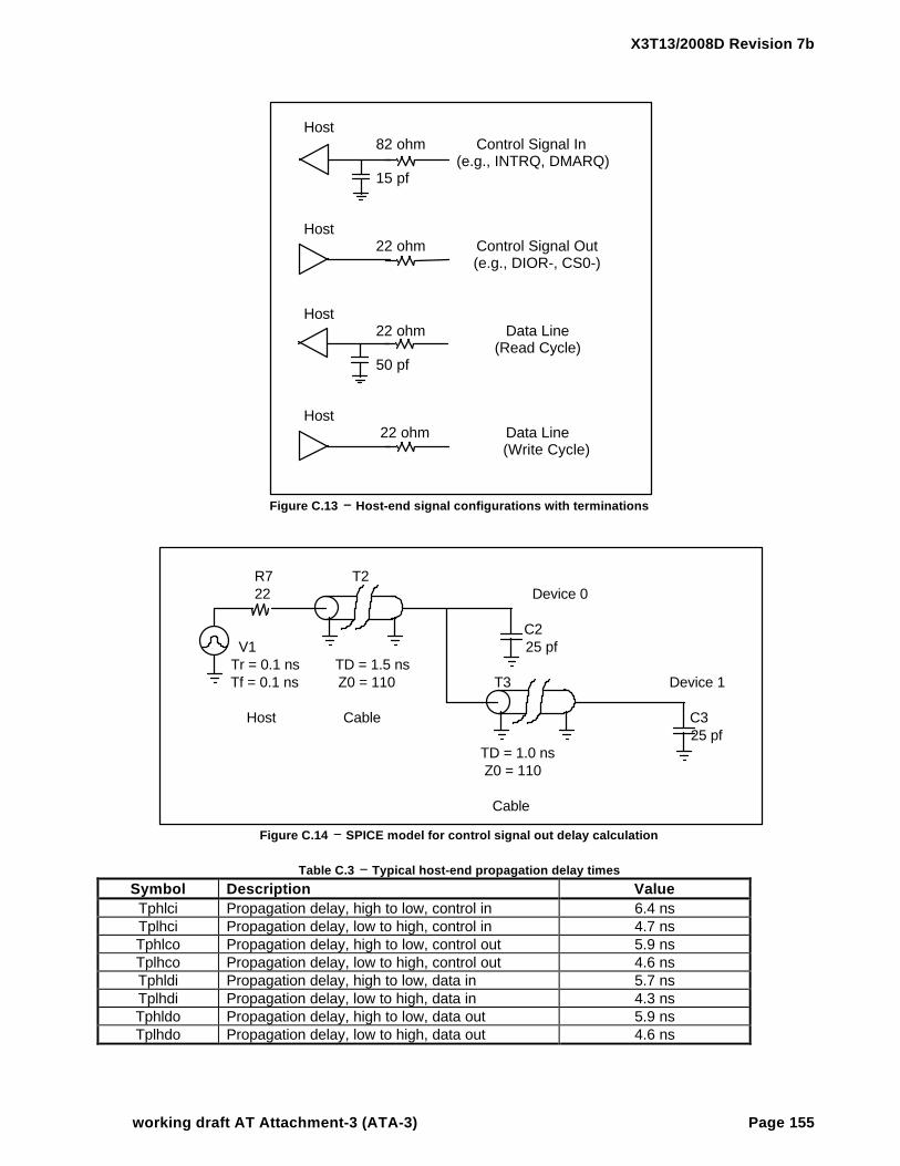
X3T13/2008D Revision 7b
working draft AT Attachment-3 (ATA-3) Page 155
Host 82 ohm Control Signal In (e.g., INTRQ, DMARQ) 15 pf
Host 22 ohm Control Signal Out (e.g., DIOR-, CS0-)
Host 22 ohm Data Line (Read Cycle) 50 pf
Host 22 ohm Data Line (Write Cycle)
Figure C.13 −− Host-end signal configurations with terminations
R7 T2 22 Device 0
C2 V1 25 pf Tr = 0.1 ns TD = 1.5 ns Tf = 0.1 ns Z0 = 110 T3 Device 1
Host Cable C3 25 pf TD = 1.0 ns Z0 = 110
Cable
Figure C.14 −− SPICE model for control signal out delay calculation
Table C.3 −− Typical host-end propagation delay times
Symbol Description ValueTphlci Propagation delay, high to low, control in 6.4 nsTplhci Propagation delay, low to high, control in 4.7 nsTphlco Propagation delay, high to low, control out 5.9 nsTplhco Propagation delay, low to high, control out 4.6 nsTphldi Propagation delay, high to low, data in 5.7 nsTplhdi Propagation delay, low to high, data in 4.3 nsTphldo Propagation delay, high to low, data out 5.9 nsTplhdo Propagation delay, low to high, data out 4.6 ns

X3T13/2008D Revision 7b
Page 156 working draft AT Attachment-3 (ATA-3)
C.2.8 Dual port cabling
One of the recent enhancements to the ATA bus has been the use of primary and secondary ports, allowingthe user to attach up to four devices. The optimal way to implement dual ports is to have two completelyseparate interfaces that have no circuitry in common. This guarantees isolation between the ports andinsures that no interference will occur.
NOTE − At the 1995 Windows Hardware Engineering Conference (WinHEC), Microsoftrecommended the use of fully independent primary and secondary ports.
The advent of local bus bridge chips has introduced new driving forces to the dual port cabling issue.Implementing two independent ATA ports on a single chip requires 66 I/O pins. Due to the cost of pins,some designs have combined the data lines of the two ports into one set of pins. Sharing the data lines (orany other lines) in this way without termination is asking for trouble. Simulations confirm that the ringing insuch configurations is large and complex, particularly if the loads on the two cables are not balanced.
One alternative pin-saving solution would be to add a set of external buffers. This would require three newcontrol lines but would save 16 data lines for a net improvement of 13 pins. This also would requireadditional packages on the circuit board.
An economical solution is to add independent series resistors for each line (see figure C.15). Energyreflected back from the first cable passes through one termination resistor before getting to the host. Thereflected signal is further attenuated as it passes through the second resistor and into the second cable. Thissignal is reflected from the end of the second cable (with loss), and must pass through the terminationresistor again before arriving at the host. This provides sufficient attenuation of reflected signals.
Primary Port Device 0 Device 1
22 ohm
Device 0 Device 1
Secondary Port
Figure C.15 −− Preferred connection for shared lines in dual port systems
Not all of the signal lines in a shared dual port interface can be shared. If the chip selects (CS0-, CS1-) andthe data strobes (DIOR-, DIOW-) are shared, then it is impossible to differentiate between the primary andsecondary ports. A write to a device on one port causes the same action to occur on the other port,destroying the data on the other device. The data strobe lines are sensitive edge-triggered signals while thechip selects act more like level-sensitive address lines. It is recommended that designers share the lesssensitive chip selects and not share the data strobes.
Table C.4 makes some assumptions about how the dual porting is being implemented. If the data lines areshared, there are not simultaneous accesses to the primary and secondary ports. This in theory allows theDMACK- and IORDY lines also to be shared. The INTRQ and DMARQ signals are driven by tristate bufferson the devices. Either Device 0 or Device 1 enables its tristate driver depending on the state of the DEV bitin the Device/Head Register. Therefore INTRQ and DMARQ cannot be shared because either Device 0 orDevice 1 will be driving these lines at all times. The primary port devices do not know about the secondaryport devices, so sharing these lines would create a conflict. In theory the DMACK- line could be shared sinceit is driven by the host. In practice this is not recommended. It is likely that some devices respond

X3T13/2008D Revision 7b
working draft AT Attachment-3 (ATA-3) Page 157
unconditionally to the DMACK- signal, whether they ever requested a DMA cycle or not. This could lead to aconflict on a DMA cycle between a primary port device and a secondary port device during the data cycle.For these reasons the INTRQ, DMARQ, and DMACK- lines cannot be shared.
Table C.4 −− Possible sharing of ATA signals in dual port configurations
Signal nameDIOR-, DIOW- Not shareable
CS0-, CS1- ShareableDA0, DA1, DA2 Shareable
DMACK- Not shareableRESET- Shareable
DD0 – DD15 ShareableDMARQ Not shareableINTRQ Not shareableIORDY Shareable
DASP-, PDIAG- Not shareableCSEL Not shareable
The DASP- lines cannot be shared. Assume there are two devices on the primary port, and one device onthe secondary port. With the DASP- lines connected, the single device on the secondary port will incorrectly“see” Device 1 on the primary port. This would be a problem for all manufacturers who follow the ATAspecifications. Similar problems can occur with the PDIAG- lines; they cannot be shared.
C.3 Crosstalk
Crosstalk is switching on one signal line causing induced signals in an adjacent line. Crosstalk has not beena significant issue in the past with slower edge rates; in newer systems the problem is often masked byringing. Once the cable is terminated and the ringing is under control, then the presence of crosstalkbecomes apparent.
C.3.1 Coupling mechanisms
There are two mechanisms by which a signal couples into an adjacent line. The first is coupling capacitance,and the second is mutual inductance. As a switching signal wavefront propagates down the cable it couplesenergy into the adjacent line. Once this energy is in the second transmission line, it propagates in bothdirections: forward toward the receiver and back toward the source (see figure C.16).
Lm Cm Lm Cm Lm Cm
Figure C.16 −− Crosstalk coupling mechanisms
First the forward coupling components are examined. The voltage induced in the second transmission line isproportional to the coupling coefficient, the inductance, and the rate of change of current in the primary side.This is a negative voltage: a positive current spike in the primary line results in a negative voltage spike inthe secondary line.

X3T13/2008D Revision 7b
Page 158 working draft AT Attachment-3 (ATA-3)
The coupling capacitance between the two lines causes a current pulse in the secondary line proportional tothe capacitance and the rate of change of voltage on the primary side. A positive voltage step on the primaryline causes a positive voltage spike on the secondary line.
These two coupling mechanisms have some interesting characteristics. The polarity of the coupling isopposite for the mutual inductance and coupling capacitance. If the magnitudes of these effects arecomparable, then they will cancel, resulting in no forward crosstalk. Unfortunately, accurately computingthese values is difficult, and the easiest way to determine the actual amount of crosstalk is to measure it.The other noteworthy characteristic is that the magnitude of the coupled signal is proportional to the rate ofchange of the signal in the primary line. This is a major reason for controlling the slew rate on ATA busdrivers. Earlier it was said that ringing on the data lines is not necessarily a problem. Here it is seen that fastedge rates and ringing on the data lines can couple by crosstalk into adjacent control lines, causing controlsequence errors through mistriggering. It is unlikely crosstalk from data lines causes observable failures in alaboratory environment. But the presence of crosstalk-induced voltage spikes on the control signals reducesthe noise margin, and can increase the long-term error rate.
The amplitude of the coupled signal is proportional to the total amount of coupling capacitance and mutualinductance, and is therefore proportional to cable length. Once a line is terminated properly, ringing is nolonger a function of length. This leaves crosstalk as the major factor limiting cable length.
Reducing crosstalk involves reducing the mutual inductance, reducing the coupling capacitance, ordecreasing the source signal amplitude. Controlling the inductance and capacitance can be done by eitherkeeping the length of the cable short or by increasing the distance between conductors. Placing a groundconductor between critical signals increases the separation of the signals and also adds a shielding effectfrom the intervening ground. In the ATA environment the only control that can be exercised over the cable isto keep the length at 18 inches or less. The amplitude of the source signal cannot be reduced and stillmaintain ATA compatibility, but there is control over some elements of the source signal. Slew rate limitationreduces the high-frequency components of the source signal and therefore reduces the coupling of thesecomponents into adjacent lines. Terminating the lines reduces ringing which also decreases the amount ofenergy coupled at the ringing frequency.
C.4 Bus timing
Terminating the ATA bus has its cost. Partial terminations at the host and the device increase propagationdelays throughout the system. The ATA standard specifies that timing is referenced to the input pins of thedevice (see clause 10). This means that most of the timing issues must be addressed by systemsmanufacturers and bridge chip designers.
C.4.1 The issues
The most significant timing issue is the propagation delay of the cable. This needs to be added to the host-side timing. The SPICE model in figure C.17 shows an unterminated host with very fast rise times driving acable with worst case loads. Two unterminated devices are assumed with the maximum allowed capacitiveloading of 25 pF.
NOTE − 25 pf was specified in ATA-2.
The simulation results are shown in figure C.18. The period of the ringing is four times the propagation delayof the cable. This simulation shows a cable propagation delay of 5.6 ns. This is twice the value obtained byassuming an 18-inch cable with a propagation velocity of 60% c. The additional delay is due to the presenceof the capacitive loads on the cable. This result is important to system designers who take into accountworst-case cable delay when specifying the bridge chip timing.

X3T13/2008D Revision 7b
working draft AT Attachment-3 (ATA-3) Page 159
T2 Device 0
V1 C2 TD = 1.5 ns 25 pf Tr = 0.1 ns ZO = 110 T3 Tf = 0.1 ns Device 1 Cable Host C3 25 pf TD = 1.5 ns ZO = 110
Cable
Figure C.17 −− SPICE model of ATA cable with worst case loads
12 V
8 V
4 V
0 V
-4 V
-8 V
-12 V 40 ns 80 ns 120 ns 160 ns time
Figure C.18 −− Simulation of unterminated ATA cable with worst case loads
From the host point of view, all of the ATA timings are corrected by adding the propagation delay of thecable to insure that the timing is correct at the input pins of the furthest device. Figure C.19 shows a typicalcorrected result using the read cycle data setup time as an example. The ATA document specifies a setuptime at the device of 20 ns (PIO Mode 3). The remaining setup time at the host is only 8.8 ns (20 - 2 x 5.6).
C.4.2 The influence of termination
If the host has a series partial termination resistor then the bridge chip includes additional timing margin toaccount for the RC delay of that resistor. Simulations show that the incremental delay added by a seriestermination resistor at the host is approximately 0.1 ns for a 22 ohm resistor and 1.7 ns for an 82 ohmresistor.
NOTE − Assuming two device loads, 25 pF at each device, 18-inch cable, 25 pF at host
The extra delay of higher resistor values is one of the reasons that 22 ohm series resistors at the host arerecommended.

X3T13/2008D Revision 7b
Page 160 working draft AT Attachment-3 (ATA-3)
DIOR- at host
5.6 ns 8.8 ns 5.6 ns
DIOR at device
20 ns
Data at device
5.6 ns
Data at host
Figure C.19 −− Host data setup time during a read cycle
The series resistor at the host is located as close as possible to the ATA connector. To see the importanceof this, SPICE simulations are done with the stray capacitance on the driver side of the series resistor andagain with the stray capacitance on the cable side. The ringing is reduced when the stray capacitance of thehost is on the driver side of the series resistor. A related issue is the distance from the host adapter chip (orchipset) to the ATA connector. Some motherboards have the chip located up to 10 inches away from theconnector. This effectively adds another 10 inches to the 18-inch ribbon cable, resulting in an equivalentcable length of 28 inches.
NOTE − The traces on the circuit board are from 50 to 200 ohm impedance, so the electricallength of the trace cannot simply be added to the 110 ohm ribbon cable. A SPICE simulationcan be used to find the actual delay.
This additional length is not necessarily a problem. If the system manufacturer takes the extra trace delayinto account in the application of the host adapter chip, and the total capacitance is kept below the ATA hostlimit of 25 pF, then in theory there is no difference. Real-world experience indicates that this calculation israrely done. The distance from the chip to the connector is not addressed in the ATA specification. Keepingthe connector within 3 inches (by trace length) of the host adapter chip is recommended.
C.4.3 Calculating rise time
Chip designers often use a lumped capacitance model for simulating the delay of the output cell. For thesimulations this sometimes consists of adding the maximum capacitance allowed for the host and thedevices (3 x 25 pF) to an estimated capacitance value for the cable (25 pF). Simulation is then performedwith 100 pF capacitance on the output. This does not give an accurate measurement of the timing. A betterapproximation is to use an output capacitance for the motherboard, a host end termination resistor, and atransmission line to the devices (see figure C.20).
To illustrate how these models are different, suppose that the propagation delay of the output cell simulationis 2 ns too slow. The chip designer (using a 100 pF model) increases the drive current of the output devices.With enough drive current into a purely capacitive load, the 2 ns is removed, bringing the output cell timingback into spec.
Increasing the drive of the output cell in the transmission line model, the length of the cable is not increasedand nor increase the speed of signal propagation in the cable is not increased. The 2 ns required time

X3T13/2008D Revision 7b
working draft AT Attachment-3 (ATA-3) Page 161
reduction is not achieved by increasing the output drive current. Increasing the output drive current onlyincreases the edge speed, making the ringing worse at the device end (some time is gained with the fasteredge speed, but not nearly as much as is predicted with a simple capacitive load model). It is not possible todecrease the overhead by increasing the drive current.
Most ASIC designers find that simulations using the recommended model of figure C.20 show their outputcells to be faster than in models with a 100 pF load.
D6 R4 T1 D1N4148 500 K + V3 - 5 V C1 D3 R3 Buffer 25 pf D1N4148 500 K under TD = 2.5 ns test ZO = 110
D5 R7 T2 D1N4148 500K + V4 - 5 V C4 D4 R6 25 pf D1N4148 500 K TD = 0.7 ns Z0 = 110
Figure C.20 −− Recommended model for I/O cell propagation delay
C.4.4 Measuring propagation delay
Propagation delay times at the host (and at the device) are measured to the ATA standard of 0.8 V for highto low transitions and 2.0 V for low to high transitions. Many IC manufacturers measure propagation delay atthe typical switch point for TTL of 1.4 V. This is not appropriate for the ATA interface since virtually everychip manufacturer (both host and device end) has included hysteresis for noise immunity. Since both thehysteresis window and hysteresis offset of a given receiver move with process, voltage, and temperature,the only guaranteed switch points are the TTL high and low values (0.8 V and 2.0 V).
C.5 Summary of guidelines
This summary is a collection of reminders for device, system, and chipset designers. They are separatedinto three groups by relevancy. The guidelines below are not intended to be a strict mandate, but a tool tohelp everyone build compatible, reliable, high-performance products.
X3T13/2008D Revision 7b
Page 162 working draft AT Attachment-3 (ATA-3)
C.5.1 Guidelines for device designers
− Terminate signals as shown in table C.1. Consider adding capacitors to ground on these lines if theinput capacitance is less than 8 pF, or use active clamping circuits. Place these resistors as close to theATA connector as possible.
− Verify that the termination circuit used on received signals has less than 20 pF of equivalentcapacitance.
− Perform a timing analysis to verify that ATA timings are met at the input to the device. Include the timedelay due to propagation and cable termination circuits.
C.5.2 Guidelines for system designers
− Do not use any value less than 1 Kohm for pull up resistors on ATA open-collector signals such asIORDY (as per the standard).
− The ATA host adapter chip should be located as close as possible to the ATA connector. Keep the tracelength between them less than 3 inches.
− After circuit board fabrication, verify that the total input capacitance at the host is less than 25 pF.− Terminate signals as shown in figure C.1. Place these resistors as close to the ATA connector as
possible.− Perform a system timing analysis to verify that ATA timings are met at the input to the device.− For dual port implementations, terminate signals as shown in figure C.15. These resistors should be
placed as close to the ATA connector of that port as possible.− For dual port implementations, the signal lines CS0- and CS1- should be shared.− For dual port implementations, the signal lines DIOR- and DIOW- should not be shared.− For dual port implementations, do not share DASP- or PDIAG- signal lines.− For dual port implementations, perform a system timing analysis to verify that ATA timings are met at the
input of the device. In particular watch the assertion widths of DIOR- and DIOW- to insure that they meetthe specification.
− Route ATA cable away from chassis, power supplies and high speed circuits.− Use the shortest cable practical and never greater than 18 in.
C.5.3 Guidelines for chip designers
− Design I/O cells to have rise and fall times of 5 ns or more under both minimum and maximum loadconditions.
− Perform timing simulations using a transmission line load model, not a 100 pF capacitor model.− Take worst-case cable delay into account when designing the ATA interface. Ensure that ATA timing
can be met at the device-end of the cable. Provide typical application data with timing for systemmanufacturers.

X3T13/2008D Revision 7b
working draft AT Attachment-3 (ATA-3) Page 163
Annex D(informative)
Bibliography
AT Attachment Interface, ANSI X3.221-1994AT Attachment Interface with Extensions, ANSI X3.279-199xSuite of 2.5” Form Factor Specifications, SFF-8200, SFF-8201, SFF-82121)
Suite of 3.5” Form Factor Specifications, SFF-8300, SFF-8301, SFF-8302Information Specification for Phoenix EDD (Enhanced Disk Drive) Specification, SFF-8039ATA Packet Interface for CD-ROMs, SFF-8020iPC Card Standard, February 1995, PCMCIA2)
1) SFF documents are published by:SFF14426 Black Walnut Court, Saratoga, California 95070FaxAccess: 408 741-1600
2) The PC Card Standard is published by:Personal Computer Memory Card International Association2635 North First Street, Suite 209, San Jose, California 95131

X3T13/2008D Revision 7b
Page 164 working draft AT Attachment-3 (ATA-3)
Annex E(informative)
ATA command set summary
The following four tables are provided to facilitate the understanding of the ATA command set. Table E.1provides information on which command codes are currently defined. Table E.2 provides a list of all of theATA commands in order of command code. Table E.3 provides a summary of all commands with theprotocol, required use, command code and registers used for each. Table E.4 shows the status and errorbits used by each command.
Table E.1 −− Command matrixx0 x1 x2 x3 x4 x5 x6 x7 x8 x9 xA xB xC xD xE xF
0x C R R R R R R R C R R R R R R R1x C O O O O O O O O O O O O O O O2x C C C C R R R R R R R R R R R R3x C C C C R R R R R R R R C R R R4x C C R R R R R R R R R R R R R R5x C R R R R R R R R R R R R R R R6x R R R R R R R R R R R R R R R R7x C O O O O O O O O O O O O O O O8x V V V V V V V V V V V V V V V V9x C C C R C C C C C C V R R R R RAx C C C R R R R R R R R R R R R RBx C R R R R R R R R R R R R R R RCx V V V V C C C R C C C C R R R RDx R R R R R R R R R R R O O O C CEx C C C C C C C R C O R R C C C CFx V C C C C C C V V V V V V V V V
Key:C = a unique command.R = Reserved, undefined in current specifications.V = Vender specific commands.O = Obsolete.
Table E.2 −− Commands sorted by command valueCommand name Command code
NOP 00hATAPI SOFT RESET 08hRECALIBRATE 10hREAD SECTOR(S) (w/ retry) 20hREAD SECTOR(S) (w/o retry) 21hREAD LONG (w/ retry) 22hREAD LONG (w/o retry) 23hWRITE SECTOR(S) (w/ retry) 30hWRITE SECTOR(S) (w/o retry) 31hWRITE LONG (w/ retry) 32hWRITE LONG (w/o retry) 33hWRITE VERIFY 3ChREAD VERIFY SECTOR(S) (w/ retry) 40hREAD VERIFY SECTOR(S) (w/o retry) 41hFORMAT TRACK 50hSEEK 70h
(continued )

X3T13/2008D Revision 7b
working draft AT Attachment-3 (ATA-3) Page 165
Table E.2 −− Commands sorted by command value (concluded)Command name Command code
EXECUTE DEVICE DIAGNOSTIC 90hINITIALIZE DEVICE PARAMETERS 91hDOWNLOAD MICROCODE 92hSTANDBY IMMEDIATE (see note) 94h E0hIDLE IMMEDIATE (see note) 95h E1hSTANDBY (see note) 96h E2hIDLE (see note) 97h E3hCHECK POWER MODE (see note) 98h E5hSLEEP (see note) 99h E6hATAPI PACKET A0hATAPI IDENTIFY DEVICE A1hATAPI SERVICE A2hSMART B0hREAD MULTIPLE C4hWRITE MULTIPLE C5hSET MULTIPLE MODE C6hREAD DMA (w/ retry) C8hREAD DMA (w/o retry) C9hWRITE DMA (w/ retry) CAhWRITE DMA (w/o retry) CBhDOOR LOCK DEhDOOR UNLOCK DFhSTANDBY IMMEDIATE (see note) E0h 94hIDLE IMMEDIATE (see note) E1h 95hSTANDBY (see note) E2h 96hIDLE (see note) E3h 97hREAD BUFFER E4hCHECK POWER MODE (see note) E5h 98hSLEEP (see note) E6h 99hWRITE BUFFER E8hIDENTIFY DEVICE EChMEDIA EJECT EDhIDENTIFY DEVICE DMA EEhSET FEATURES EFhSECURITY SET PASSWORD F1hSECURITY UNLOCK F2hSECURITY ERASE PREPARE F3hSECURITY ERASE UNIT F4hSECURITY FREEZE F5hSECURITY DISABLE PASSWORD F6hNOTE − These commands have two command codes and appear in thistable twice, once for each command code.

X3T13/2008D Revision 7b
Page 166 working draft AT Attachment-3 (ATA-3)
Table E.3 −− Command codes and parametersproto Command typ Command Parameters used
code FR SC SN CY DHND CHECK POWER MODE O 98h E5h y DND DOOR LOCK O DEh DND DOOR UNLOCK O DFh DPO DOWNLOAD MICROCODE O 92h y y y y DND EXECUTE DEVICE DIAGNOSTIC M 90h D*VS FORMAT TRACK V 50h dPI IDENTIFY DEVICE M ECh D
DM IDENTIFY DEVICE DMA O EEh DND IDLE O 97h E3h y DND IDLE IMMEDIATE O 95h E1h DND INITIALIZE DEVICE PARAMETERS M 91h y yND MEDIA EJECT O EDh DND NOP O 00h DPI READ BUFFER O E4h D
DM READ DMA (w/ retry) M C8h y y y yDM READ DMA (w/o retry) M C9h y y y yPI READ LONG (w/ retry) O 22h y y y yPI READ LONG (w/o retry) O 23h y y y yPI READ MULTIPLE M C4h y y y yPI READ SECTOR(S) (w/ retry) M 20h y y y yPI READ SECTOR(S) (w/o retry) M 21h y y y yND READ VERIFY SECTOR(S) (w/ retry) M 40h y y y yND READ VERIFY SECTOR(S) (w/o retry) M 41h y y y yND RECALIBRATE O 10h DPO SECURITY DISABLE PASSWORD O F6h DND SECURITY ERASE PREPARE O F3h DPO SECURITY ERASE UNIT O F4h DND SECURITY FREEZE O F5 DPO SECURITY SET PASSWORD O F1H DPO SECURITY UNLOCK O F2h DND SEEK M 70h y y yND SET FEATURES M EFh y DND SET MULTIPLE MODE M C6h y DND SLEEP O 99h E6h DND SMART DISABLE OPERATIONS O 0B0h y y DND SMART ENABLE/DISABLE AUTOSAV O 0B0h y y y DND SMART ENABLE OPERATIONS O 0B0h y y DPI SMART READ THRESHOLDS O 0B0h y y DPI SMART READ VALUES O 0B0h y y DND SMART RETURN STATUS O 0B0h y y DND SMART SAVE VALUES O 0B0h y y DND STANDBY O 96h E2h y DND STANDBY IMMEDIATE O 94h E0h DPO WRITE BUFFER O E8h DDM WRITE DMA (w/ retry) M CAh y y y yDM WRITE DMA (w/o retry) M CBh y y y yPO WRITE LONG (w/ retry) O 32h * y y y yPO WRITE LONG (w/o retry) O 33h * y y y y
(continued)

X3T13/2008D Revision 7b
working draft AT Attachment-3 (ATA-3) Page 167
Table E.3 −− Command codes and parameters (concluded)proto Command typ Command Parameters used
code FR SC SN CY DHPO WRITE MULTIPLE M C5h * y y y yPO WRITE SECTOR(S) (w/ retry) M 30h * y y y yPO WRITE SECTOR(S) (w/o retry) M 31h * y y y yPO WRITE VERIFY O 3Ch * y y y yVS Vendor specific V 9Ah,C0h-C3h,8xh,
F0h-FFh- Reserved: all remaining codes R
Key:DM = DMA command ND = Non-data command PI = PIO data in commandPO = PIO data out command VS = Vendor specific command O = OptionalM = Mandatory R = Reserved V = Vendor specific implementationCY = Cylinder registers SC = Sector Count register DH = Device/Head registerSN = Sector Number register FR = Features register (see command descriptions for use)y = the register contains a valid parameter for this command. For the Device/Head register, y means both the deviceand head parameters are used.D = only the device parameter is valid and not the head parameter.d = the device parameter is valid, the usage of the head parameter vendor specific.D* = Addressed to device 0 but both devices execute it.* = Maintained for compatibility (see 5.2.10)
Table E.4 −− Status and error usageStatus register Error register
DRDY DF CORR ERR UNC IDNF ABRT TK0NF AMNF
ACKNOWLEDGE MEDIACHANGE
V V V V
BOOT - POST-BOOT V V V VBOOT - PRE-BOOT V V V VCHECK POWER MODE V V V VDOOR LOCK V V V VDOOR UNLOCK V V V VDOWNLOAD MICROCODE V V V VEXECUTE DEVICEDIAGNOSTIC
V V V (see 7.5)
FORMAT TRACK V V V V V V V VIDENTIFY DEVICE VIDENTIFY DEVICE DMA VIDLE V V V VIDLE IMMEDIATE V V V VINITIALIZE DEVICEPARAMETERS
V V
MEDIA EJECT V V V VNOP V V V VREAD BUFFER V V V VREAD DMA (w/ retry) V V V V V V V VREAD DMA (w/o retry) V V V V V V V VREAD LONG (w/ retry) V V V V V VREAD LONG (w/o retry) V V V V V VREAD MULTIPLE V V V V V V V VREAD SECTOR(S) (w/ retry) V V V V V V V VREAD SECTOR(S) (w/oretry)
V V V V V V V V
(continued)

X3T13/2008D Revision 7b
Page 168 working draft AT Attachment-3 (ATA-3)
Table E.4 −− Status and error usage (concluded)Status register Error register
DRDY DF CORR ERR UNC IDNF ABRT TK0NF AMNF
READ VERIFY SECTOR(S)(w/ retry)
V V V V V V V V
READ VERIFY SECTOR(S)(w/o retry)
V V V V V V V V
RECALIBRATE V V V V VSECURITY DIS PASSWORD V V V VSECURITY ERASE PREP V V V VSECURITY ERASE UNIT V V V VSECURITY FREEZE V V V VSECURITY SET PASSWRD V V V VSECURITY UNLOCK V V V VSEEK V V V V VSET FEATURES V V V VSET MULTIPLE MODE V V V VSLEEP V V V VSMART DISABLE OPS V V VSMART EN/DIS AUTOSAVE V V VSMART ENABLE OPS V V VSMART READ THRSHOLDS V V V VSMART READ VALUES V V V VSMART RETURN STATUS V V VSMART SAVE VALUES V V V V V VSTANDBY V V V VSTANDBY IMMEDIATE V V V VWRITE BUFFER V V V VWRITE DMA (w/ retry) V V V V VWRITE DMA (w/o retry) V V V V VWRITE LONG (w/ retry) V V V V VWRITE LONG (w/o retry) V V V V VWRITE MULTIPLE V V V V VWRITE SECTOR(S) (w/ retry) V V V V VWRITE SECTOR(S)(w/o retry)
V V V V V
WRITE VERIFY V V V V V V V VInvalid command code V V V VKey: V = valid on this command