To: X3T10 SPI-2 Study Group X3T10-95-315r0 From: … · Lower case is used for words having the...
52
Page 1 To: X3T10 SPI-2 Study Group X3T10-95-315r0 From: Bill Ham, Digital Equipment Date: September 11, 1995 Subject: Revised proposal for SPI-2 electrical interface
Transcript of To: X3T10 SPI-2 Study Group X3T10-95-315r0 From: … · Lower case is used for words having the...

Page 1
To: X3T10 SPI-2 Study Group X3T10-95-315r0
From: Bill Ham, Digital Equipment
Date: September 11, 1995
Subject: Revised proposal for SPI-2 electrical interface

Page 2
Proposed Working X3T10/xxxxDDraft
Revision 02bSeptember 11, 1995
Information Technology -SCSI Parallel Interconnect 2 (SPI-2)
This is an internal working document of X3T10, a Technical Committee X3T10 of the AccreditedStandards Committee X3. As such, this is not a completed standard and has not been approvedby Technical Committee X3T10. The contents may be modified by the X3T10 TechnicalCommittee. This document is made available for review and comment only.
Permission is granted to members of X3, its technical committees, and their associated taskgroups to reproduce this document for the purposes of X3 standardization activities withoutfurther permission, provided this notice is included. All other rights are reserved. Any duplicationfor commercial or for-profit use is prohibited.
[Technical Editor's Note: This Rev contains all the technical information presently available to theeditor as of September 8, 1995 and needs significant additional technical work. This is the firstdraft and it contains (almost without editing) a draft of a version of a subset of a multidrop LVDSspecification being developed by TIA (supplied by Kevin Gingrich and John Goldie).
ASC X3T10 Technical Editor:Bill HamDigital Equipment334 South Street.Shrewsbury, MA 01545
Voice (508) 841-2629Fax (408) 841-5266Email [email protected]
Reference numberISO/IEC ***** : 199x
ANSI X3.*** - 199xPrinted 04/18/98

Page 3
Other Points of Contact:X3T10 Chair X3T10 Vice-ChairJohn Lohmeyer Lawrence J. LamersSymbios Logic Adaptec1635 Aeroplaza Drive 691 South Milpitas BlvdColorado Springs, CO 80916 San Jose, CA 95035
Voice: 719 573-3362 408 957-7817Fax: 719 597-8225 408 957-7193Email: [email protected]
X3 SecretariatLynn BarraAdministrator Standards ProcessingX3 Secretariat Telephone: 202-626-57381250 Eye Street, NW Suite 200 Facsimile: 202-638-4922Washington, DC 20005
SCSI ReflectorInternet address for subscription to the SCSI reflector: [email protected] address for distribution via SCSI reflector: [email protected]
SCSI Bulletin Board 719-574-0424
Document DistributionGlobal Engineering Telephone: 303-792-2181or15 Inverness Way East 800-854-7179Englewood, CO 80112-5704 Facsimile: 303-792-2192
ABSTRACTThis document describes the physical layer of the SCSI Parallel Interface 2 which extends andsupercedes earlier standards relating to this subject.
PATENT STATEMENTCAUTION: The developers of this standard have requested that holder's of patents that may berequired for the implementation of the standard, disclose such patents to the publisher. However, neither the developers nor the publisher have undertaken a patent search in order toidentify which, if any, patents may apply to this standard.As of the date of publication of this standard and following calls for the identification of patentsthat may be required for the implementation of the standard, no other such claims have beenmade. No further patent search is conducted by the developer or the publisher in respect to anystandard it processes. No representation is made or implied that licenses are not required toavoid infringement in the use of this standard.

Page 4
Contents1. Scope ...........................................................................................................................................102. Normative references ...................................................................................................................103. Definitions, symbols and abbreviations .......................................................................................10
3.1 Definitions ............................................................................................................................103.2 Symbols and Abbreviations.................................................................................................103.3 Conventions.........................................................................................................................11
4. General.........................................................................................................................................115. Physical interconnect ...................................................................................................................11
5.1 Cable media.........................................................................................................................115.2 Connectors ..........................................................................................................................12
6. Bus termination ............................................................................................................................126.1 Termination power...............................................................................................................126.2 Single ended bus termination..............................................................................................126.3 Low voltage differential bus termination ..............................................................................13
7. Bus drivers and receivers.............................................................................................................157.1 Single ended drivers............................................................................................................15
7.1.1 Assertion and negation drivers ..................................................................................157.1.2 Ground drivers ...........................................................................................................15
7.2 Single ended receivers ........................................................................................................157.3 Low voltage differential drivers ............................................................................................157.4 Low voltage differential receivers.........................................................................................17
8. Transmission mode detection......................................................................................................188.1 LV DIFFSENS driver ............................................................................................................198.2 LV DIFFSENSE receiver ......................................................................................................19
9. Contact assignments....................................................................................................................2010. LV diferential configuration rules................................................................................................2311. SCOPE .......................................................................................................................................2912. NORMATIVE REFERENCES ......................................................................................................3013. DEFINITIONS, SYMBOLS AND ABBREVIATIONS.....................................................................30
13.1 Data signaling rate.............................................................................................................3013.2 DTE ....................................................................................................................................3013.3 DCE ...................................................................................................................................3013.4 LVDS-M..............................................................................................................................3013.5 Star (*) ...............................................................................................................................30
14. APPLICABILITY...........................................................................................................................3114.1 General applicability ..........................................................................................................3114.2 Data signaling rate.............................................................................................................31
15. ELECTRICAL CHARACTERISTICS.............................................................................................3215.1 Generator characteristics...................................................................................................32
15.1.1 Open-circuit output voltages, VOA and VOB ...............................................................3315.1.2 Differential output voltage, Vt....................................................................................3415.1.3 Offset (common-mode output) voltage, VOS.............................................................3515.1.4 Short-circuit currents, ISA and ISB ..............................................................................3515.1.5 Off-state output currents, IOFFA and IOFFB ...................................................................3615.1.6 Output signal waveform ...........................................................................................3615.1.7 Dynamic output signal balance................................................................................37
15.2 Receiver characteristics.....................................................................................................3815.2.1 Receiver input voltage threshold, VIT........................................................................3915.2.2 Receiver input currents, Iia and Iib .............................................................................40
15.3 Generator/receiver output/input currents, IOFFA/A' and IOFFB/B' ..............................................4115.4 Interconnecting media electrical characteristics ...............................................................41
15.4.1 Characteristic impedance ........................................................................................42

Page 5
15.4.2 Attenuation ...............................................................................................................4215.4.3 Additional parameters ..............................................................................................42
15.5 System characteristics.......................................................................................................4215.5.1 Media termination characteristics ............................................................................4215.5.2 Terminating interchanges.........................................................................................4215.5.3 Interchange input impedance ..................................................................................4415.5.4 Total load limit ..........................................................................................................4515.5.5 Failsafe operation.....................................................................................................45
16. CIRCUIT PROTECTION..............................................................................................................4517. OPTIONAL GROUNDING ARRANGEMENTS.............................................................................45
17.1 Signal common (ground) ..................................................................................................4517.1.1 Configuration "A" ......................................................................................................4517.1.2 Configuration "B" ......................................................................................................46
17.2 Shield ground - cable applications....................................................................................4618. ANNEX A (informative) ...............................................................................................................47
18.1 Interconnecting cable ........................................................................................................4718.1.1 Length ......................................................................................................................4718.1.2 Typical cable characteristics ....................................................................................47
18.1.2.1 Parallel interface cable ...................................................................................4718.1.2.1.1 Parallel cable, physical characteristics .................................................4718.1.2.1.2 Parallel cable, electrical characteristics ................................................47
18.1.2.2 Serial interface cable ......................................................................................4818.1.2.2.1 Serial cable, physical characteristics ....................................................4818.1.2.2.2 Serial cable, electrical characteristics ...................................................48
18.1.3 Cable termination .....................................................................................................4818.2 Cable length vs. data signaling rate guidelines.................................................................4818.3 Co-directional and contra-directional timing information ..................................................4918.4 In both cases the clock should transition as close to the center of the data bit as possible.49
19. ANNEX B (informative) ...............................................................................................................5019.1 Compatibility with other interface standards .....................................................................50
19.1.1 Generator output levels (figure B.1) .........................................................................5019.1.2 Compatibility with IEEE 1596.3 ................................................................................5119.1.3 Compatibility with other interface standards............................................................51
19.2 Power dissipation of generators ........................................................................................5219.3 Related TIA/EIA standards.................................................................................................5219.4 Other related interface standards ......................................................................................52

Page 6
FiguresFigure 1 - LVDF terminator example ................................................................................................13Figure 2 - Terminator bias generator characteristics .......................................................................14Figure 3 - Universal driver architecture ............................................................................................17Figure 4 - LV receiver example.........................................................................................................18Figure 5 - LV DIFFSENS receiver .....................................................................................................20
Page 7
TablesTable 1 - Bit ordering in a byte .........................................................................................................11Table 2 - LVDF terminator specifications .........................................................................................14Table 3 - Terminator bias generator specifications..........................................................................14Table 4 - LV differential driver operating specifications ...................................................................16Table 5 - LV differential receiver operating specifications................................................................18Table 6 - DIFFSENS driver specifications ........................................................................................19Table 7 - DIFFSENS input levels ......................................................................................................19Table 8 - Low voltage differential contact assignments - P cable ....................................................21Table 9 - Low voltage differential contact assignments - A cable ....................................................22

Page 8
Foreword
Clause 1 defines the scope of the SCSI parallel interface 2 (SPI-2).Clause 2 specifies the normative references.Clause 3 defines the definitions, symbols and abbreviations.Clause 4 describes the relationship of SPI-2 to other SCSI standard documentsClause 5.Clause 6Clause 7Clause 8Annexes.
Page 9
Introduction
A major goal of the SPI-2 standard is to define a physical layer acceptable to device andsubsystem vendors, looking for an incremental evolution from present parallel SCSIThe essential characteristics:
• Miminum disruption to installed base software and hardware
• Cost parity with single ended in all forms including differential
• Enabling a single physical interface for both single ended and differential
• Enabling more flexible use of TERMPWR
• Enabling data phase transmission speed up to 80 Megatransfers/sec (160Megabytes/sec)
• Enabling operation with low voltage silicon chips and low voltage power (3.3 V)
• Specifying a sensing scheme that allows devices to detect the type of bus (singleended/differential) and to automatically set their transceivers to the appropriate type.
• Enabling the use of much smaller cables and connectors
• Enabling the direct, blind hot plugging of devices into backplanes
This standard (SPI-2) defines the following functions:
• The physical medium, clocking, line drivers/receivers, connectors and cables.
The following functions are defined by the upper-level protocol specified in SCSI-3 SIP:
• The interpretation of the SDTR parameters requried for FAST 40 and FAST 80 operation.
Page 10
Information Processing Systems - SCSI Parallel Interface 2 (SPI-2)
1. Scope
This document defines the physical layer of the SCSI Parallel Interface operating at all speedsdefined by SCSI-2, SCSI-3 SPI, and SCSI-3 FAST 20 and adding two new speed ranges: FAST 40and FAST 80.
2. Normative references
This standard references the following standards:SCSI-3 Architecture ModelSCSI-3 Command Set documentsAll references made in this standard to a Command Descriptor Block (CDB) refer to those CDB'sand CDB formats defined in the SCSI-2 or SCSI-3 standards documents.ANSI/EIA 364, entitled “Electrical Connector Test Procedures Including EnvironmentalClassifications”
3. Definitions, symbols and abbreviations
3.1 Definitions
3.1.1. application: A process that is communicating via the SPI-2 physical layer.
3.1.2. Need other terms for this list
3.2 Symbols and Abbreviations
CMOS complementary metal oxide semiconductor.DMA direct memory accessEMI electro-magnetic interferenceESD electro-static dischargeFCS fiber channel standardFDDI fiber distributed data interfaceIDC insulation displacement connector.LSI large scale integrationPOR power-on resetPOST power-on self-testRAS reliability, availability and serviceabilityRFI radio-frequency interferenceSCSI Small Computer Systems Interface& Logical AND= Assignment or comparison for EQUAL≠ Comparison for NOT EQUAL< Comparison for LESS THAN≤ Comparison for LESS THAN OR EQUAL TO> Comparison for GREATER THAN+ ADD- SUBTRACT* MULTIPLY± PLUS OR MINUS≈ APPROXIMATELY

Page 11
» MUCH GREATER THAN
3.3 Conventions
Certain words and terms used in this standard have a specific meaning beyond the normalEnglish meaning. These words and terms are defined either in the glossary or in the text wherethey first appear. Lower case is used for words having the normal English meaning.
Numbers that are not immediately followed by lower-case "b" or "h" are decimal values.
Numbers immediately followed by lower-case "b" (xxb) are binary values.
Numbers immediately followed by lower-case "h" (xxh) are hexadecimal values.
Decimal numbers are indicated with a comma( e.g., two and one half is represented as "2,5). Decimal numbers having a value exceeding 999 are represented with a space (e.g., 24 255).
The bit ordering used in SCSI is defined in table 1.
Table 1 - Bit ordering in a byte7 6 5 4 3 2 1 0
msb lsb
4. General
SCSI defines a parallel interface for use within present and future storage sub-systems
This standard describes the physical layer of SCSI. It is intended for use with SCSI-3 interlockedprotocol or any earlier version of SCSI protocol.
This standard is intended to provide a complete specification of the physical layer for all SCSIimplementations that are currently supported by X3T10. It will incorporate the relevant technicalsections relating to the physical layer of the following documents:
SCSI-2 The complete SCSI specification including proptocol and physical
SCSI-3 SPI The specification for Fast single ended SCSI and the single 16 bit cable system
SCSI-3FAST 20
The specification allowing operation of SCSI-2 and SCSI-3 SPI systems with dataphase transmissions up to 20 Megatransfers/sec
5. Physical interconnect
5.1 Cable media
The same cable and interconnect media specified in SCSI-3 SPI and SCSI-3 FAST 20 shall beused for all interconnect except where specified in this document.

Page 12
5.2 Connectors
All the connectors specified in SCSI-2 and SCSI-3 SPI shall be allowed.
[Editor's note: Additional shielded device and cable connectors based on the VHDCI are expectedto be submitted as proposals]
[Editor's note: Additional unshielded device and cable/backplane connectors based on the 80 pinSCA-2 connector are expected to be submitted as proposals]
6. Bus termination
6.1 Termination power
All bus terminators shall be powered from at least one source of termination power. TheTERMPWR lines in the cable are available for distribution of termination power. Direct connectionbetween the termination power source and the individual terminators without using the TERMPWRline is also allowed.
If the termination power source is connected to the cable TERMPWR line, the source shall beisolated in a manner that prevents sinking of current from the TERMPWR line if the terminationpower source falls below the voltage existing on the TERMPWR line.
[Implementor's note: This requirement is frequently met by using diode isolation]
Termination power sources and the associated power distribution scheme used shall be capableof delivering adequate voltage and current to allow the terminator(s) to meet the requirementsspecified in SCSI-3 SPI under the designed application conditions.
[Implementor's note: Annex A provides guidance for the tradeoffs between terminator sourcevoltage, terminator input requirements, wire gauge, bus width, and number of connectors in theTERMPWR path.]
The TERMPWR lines may be used for distribution of power for purposes other than for SCSI bustermination as long as the bus wiring and wire gauge comply with section xxxx and the voltageand current delivered to the SCSI bus terminators remain adequate to supply the requirements ofthe terminators.
Profiles of different use conditions are described in Annex A. These profiles restrict theimplementation parameters for TERMPWR distribution.
6.2 Single ended bus termination

Page 13
The single ended SCSI bus termination shall follow the specifications set forth in SCSI-3 SPI orSCSI-3 FAST 20 where applicable.
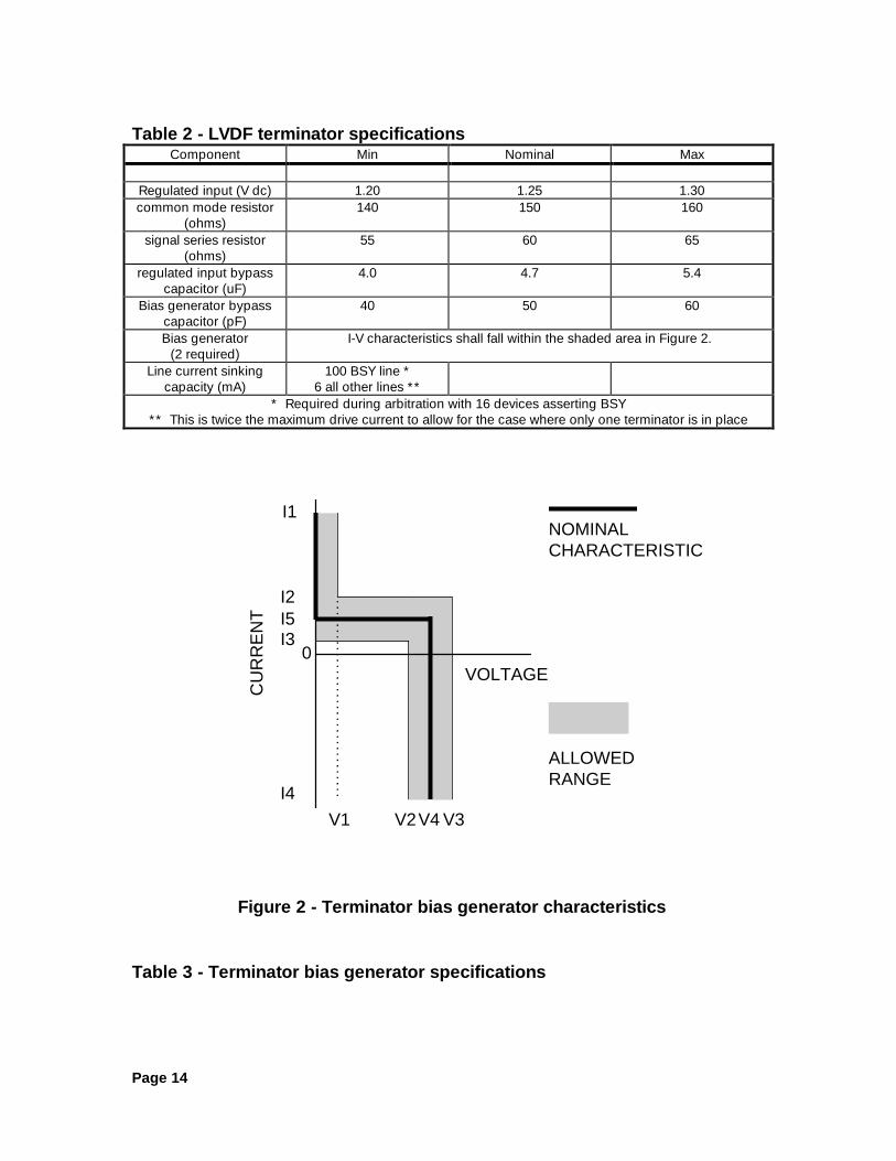
6.3 Low voltage differential bus termination
When operating in the low voltage differential mode SCSI bus termination specified in this sectionshall be used.
Figure 1 - LVDF terminator example
1.25 V REG=
250 uA
0 uA0 V
75 mV
60 OHM
60 OHM
150 OHM
4.7 uF
50 pF
50 pF
- SIGNAL
+ SIGNAL
+
+
+
I
VBIASGENERATOR
Page 14
Component Min Nominal Max
Regulated input (V dc) 1.20 1.25 1.30common mode resistor
(ohms)140 150 160
signal series resistor(ohms)
55 60 65
regulated input bypasscapacitor (uF)
4.0 4.7 5.4
Bias generator bypasscapacitor (pF)
40 50 60
Bias generator(2 required)
I-V characteristics shall fall within the shaded area in Figure 2.
Line current sinkingcapacity (mA)
100 BSY line *6 all other lines **
* Required during arbitration with 16 devices asserting BSY** This is twice the maximum drive current to allow for the case where only one terminator is in place
Figure 2 - Terminator bias generator characteristics
Table 2 - LVDF terminator specifications
CU
RR
EN
T
VOLTAGE0
I1
I2
I3
I4
V1 V2 V3
NOMINALCHARACTERISTIC
I5
V4
ALLOWEDRANGE
Table 3 - Terminator bias generator specifications

Page 15
Parameter ValueI1 3 mAI2 270 uAI3 230 uAI4 - 3 mAI5 250 uAV1 10 mVV2 65 mVV3 85 mVV4 75 mV
7. Bus drivers and receivers
7.1 Single ended drivers
7.1.1 Assertion and negation drivers
The single ended assertion and negation drivers shall follow the specifications in SCSI-3 SPI andSCSI-3 FAST20. Single ended drivers are not specified for speeds higher than FAST 20.
7.1.2 Ground drivers
When using the universal driver architecture described in Figure 3 a new single ended driver isrequired for the ground side of the driver. This so called ground driver provides the connection toground for the single ended ground line associated with the - signal line. In a non-universal singleended driver condition this ground connection is provided by a hard ground. With a universaldriver, this pin may not be hard grounded or the differential mode will not operate properly.
Ground drivers shall have on resistances of less than 20 ohms and shall remain on for the entiretime the device is powered and used in a single ended transmission mode. Ground drivers arenot required to implement any slew rate controls but they must meet all of the input leakage andvoltage level requirements for the LVDF mode specified in this document.
Since the drive requirements for ground drivers are not tightly specified it may be convenient toadjust the size of the ground driver implementation to acheive the desired capacitive balancecondition for the LVDF between the + signal and - signal pins.
7.2 Single ended receivers
Single ended receivers shall follow the specfications in SCSI-3 SPI and SCSI-3 FAST20. Singleended receivers are not specified for operation at speeds higher than FAST20.
7.3 Low voltage differential drivers

Page 16
Low voltage differential drivers shall conform to the architecture specified in Figure 3. It is notrequired to implement the single ended drivers with the LV differential drivers but it is allowed toimplement both LV differential drivers and single ended drivers in a single device.
The LV differential driver consists of balanced current sources that source current from VCC toone signal line while sinking the same current to ground from the other signal line. Diagonallyopposite sources operate together to produce a signal assertion or a signal negation. Anassertion is produced when VCC current is sourced to the + signal line and the - signal linereturns current to ground. A negation is produced when VCC current is sourced to the - signalline and the + signal line returns current to ground.
This scheme produces dc differential voltage levels of 480 to 720 mV with a common mode levelof nominally 1,25 volts when used with the termination scheme specified in section 6.3 without thebias generator. Adding the bias generator (required) increases the spread by nominally 150 mVon each end (330 mV to 970 mV).
Drivers shall negate previously asserted signals for at least a bus settle delay prior to returning tothe high impedance state. [This requirement is caused by the low bias current available from theterminators.]
LV differential drivers shall meet the specifications in Table 4 and all the specifications in Annex B.
Parameter max nominal min NotesOn current (mA) 6.0 5 4.0 under bus
operatingconditions
Off current (uA) 10 @SE Vin < 3.3Voff to on skew
- signal to + signal50 pS
on to off skew- signal to + signal
50 pS
Current imbalance * 500 uA @ 1.25 Vcommon mode
compliance voltage2.175 0.225
* Difference in the magnitude of the + signal current and the - signal current at the connector nearest thedriver
Table 4 - LV differential driver operating specifications

Page 17
Figure 3 - Universal driver architecture
7.4 Low voltage differential receivers
Low voltage differential receivers shall meet the specifications in Table 5 and the specifications inAnnex B.
GROUND
SINGLEENDEDGROUNDDRIVER
LVDF SIGNAL DRIVERS
SINGLEENDEDNEGATIONDRIVER
SINGLEENDEDASSERTIONDRIVER
VCC
GND :SINGLE ENDED: - SIGNAL+ SIGNAL :LVDF: - SIGNAL

Page 18
Parameter Maximum Nominal Minimum NotesInput voltage (dcsingle ended))
4.0 abs max
input sensitivity *(differential mV)
100 dc over commonmode range
Input voltage(differential V)
±3.3 0 See test circuit(need test circuit)
Common mode dcV
2.35 0.05 See test circuit(need test circuit)
input leakagecurrent (uA)
10 @0 to VCC to localground each input
* This is the smallest input level guaranteed to produce a detection by the receiver -- smaller numbersindicate greater sensitivity so only the minimum sensitivity is specified
Implementor'snote: LV differential receivers will usually be implemented as shown in Figure 4.
Figure 4 - LV receiver example
8. Transmission mode detection
Table 5 - LV differential receiver operating specifications
- SIGNAL+SIGNAL
LOCAL GROUND
TO LOGIC
BIAS CURRENT
Page 19
8.1 LV DIFFSENS driver
The LV DIFFSENS driver sets a voltage level on the DIFSENS line that uniquely defines a LVdifferential transmission mode. All LV differential terminators shall provide a LV DIFFSENS driveraccording to the specifications in Table 6.
Parameter max nominal min notesoutput voltage se 1.4 1.3 1.2
Output currentsource dc
15 mA 5 mA With TERMPWR @operational levelsand DIFFSENS @
1.2 to 1.4 VInput current dc 10 uA with terminator
disabledInput sink current
dc(Noise load)
200 uA @ DIFFSENS =2.75 V
8.2 LV DIFFSENSE receiver
All LV differential devices shall incorporate the LV DIFFSENSE receiver that detects the voltagelevel on the DIFFSENS line for purposes of informing the device of the transmission mode beingused by the bus. The LV differential DIFFSENS receiver shall be capable of detecting singleended, LV differential, and HV differential modes. Table 7 defines the receiver input levels for eachof the three modes.
Mode Single ended HV differential LV differentialDIFFSENS line GROUND (< 0.5 V dc) 5V pull up through 1K
(> 2.5 V dc)0.7 to 1.9 V dc
All voltages measured at the device connector with respect to local ground
The LV DIFFSENS receiver shall incorporate low pass with a minimum of 2 mS time constant tolocal ground. [This requirement provides ac common mode protection to the DIFFSENS functionand allows ac receiver common mode levels much greater than 0.5 V.] LV DIFFSENS receiversshall provide 200 K ohms minimum to local ground for purposes of providing ground reference ifno DIFFSENS drivers are connected to the bus. Higher values are allowed if the system integratorcan guarantee that the resistor value chosen will overcome all leakage from devices on the busand will therefore produce reliable single ended detection (see Table 7).
A typical implementation of a LV DIFFSENS receiver is shown in Figure 5.
Table 6 - DIFFSENS driver specifications
Table 7 - DIFFSENS input levels
Page 20
Figure 5 - LV DIFFSENS receiver
9. Contact assignments
20 K
DIFFSENSLINE
0.1uF
1.9 TO 2.2 V
0.6 TO 0.7 V
+
-
+
-
HIGHVOLTAGEDIFFERENTIAL
LOW VOLTAGEDIFFERENTIAL
SINGLEENDED
RECEIVER INPUTS HIGHIMPEDANCE AT ALL TIMES(< 30 uA @ 0 to 2.75 V)
200 K

Page 21
Signal name Connectorcontactnumber
Cable conductor number Connectorcontactnumber
Signal name
+DB(12) 1 1 2 35 - DB(12)+DB(13) 2 3 4 36 -DB(13)+DB(14) 3 5 6 37 -DB(14)+DB(15) 4 7 8 38 -DB(15)+DB(P1) 5 9 10 39 -DB(P1)+DB(0) 6 11 12 40 -DB(0)+DB(1) 7 13 14 41 -DB(1)+DB(2) 8 15 16 42 -DB(2)+DB(3) 9 17 18 43 -DB(3)+DB(4) 10 19 20 44 -DB(4)+DB(5) 11 21 22 45 -DB(5)+DB(6) 12 23 24 46 -DB(6)+DB(7) 13 25 26 47 -DB(7)+DB(P) 14 27 28 48 -DB(P)
GROUND 15 29 30 49 GROUNDDIFFSENS 16 31 32 50 GROUNDTERMPWR 17 33 34 51 TERMPWRTERMPWR 18 35 36 52 TERMPWRRESERVED 19 37 38 53 RESERVEDGROUND 20 39 40 54 GROUND
+ATN 21 41 42 55 -ATNGROUND 22 43 44 56 GROUND
+BSY 23 45 46 57 -BSY+ACK 24 47 48 58 -ACK-RST 25 49 50 59 -RST
+MSG 26 51 52 60 -MSG+SEL 27 53 54 61 -SEL+C/D 28 55 56 62 -C/D+REQ 29 57 58 63 -REQ+I/O 30 59 60 64 -I/O
+DB(8) 31 61 62 65 -DB(8)+DB(9) 32 63 64 66 -DB(9)
+DB(10) 33 65 66 67 -DB(10)+DB(11) 34 67 68 68 -DB(11)
Table 8 - Low voltage differential contact assignments - P cable

Page 22
Signal name Connectorcontactnumber
Cable conductor number Connectorcontactnumber
Signal name
SET 1 SET 2 SET 2 SET 1+DB(0) 1 1 1 2 26 2 -DB(0)+DB(1) 3 2 3 4 27 4 -DB(1)+DB(2) 5 3 5 6 28 6 -DB(2)+DB(3) 7 4 7 8 29 8 -DB(3)+DB(4) 9 5 9 10 30 10 -DB(4)+DB(5) 11 6 11 12 31 12 -DB(5)+DB(6) 13 7 13 14 32 14 -DB(6)+DB(7) 15 8 15 16 33 16 -DB(7)+DB(P) 17 9 17 18 34 18 -DB(P)
GROUND 19 10 19 20 35 20 GROUNDDIFFSENS 21 11 21 22 36 22 GROUNDRESERVED 23 12 23 24 37 24 RESERVEDTERMPWR 25 13 25 26 38 26 TERMPWRRESERVED 27 14 27 28 39 28 RESERVEDGROUND 29 15 29 30 40 30 GROUND
+ATN 31 16 31 32 41 32 -ATNGROUND 33 17 33 34 42 34 GROUND
+BSY 35 18 35 36 43 36 -BSY+ACK 37 19 37 38 44 38 -ACK-RST 39 20 39 40 45 40 -RST
+MSG 41 21 41 42 46 42 -MSG+SEL 43 22 43 44 47 44 -SEL+C/D 45 23 45 46 48 46 -C/D+REQ 47 24 47 48 49 48 -REQ+I/O 49 25 49 50 50 50 -I/O
Table 9 - Low voltage differential contact assignments - A cable
Page 23
10. LV diferential configuration rules
The overall distance between terminators shall be a maximum of 35 meters.
[The real length limits are likely to be determined by attenuation limits and are not known at thistime for all different loading conditions. Data exists that shows 25 meters is acheivable with lessthan a 2x attenuation at FAST 100 speeds using the drivers specified in this document on standardSCSI parallel twisted pair cable. There is at least a 3x attenuation allowed worst case with thepresent specifications in this document so the protocol limit of approximately 35 meters may notbe unreasonable.]
The difference in stub length for devices shall be less than 0.5 inches from the device connector tothe bonding pad on the silicon chip for the REQ, ACK, DATA and PARITY signals.
The difference in capacitance to local ground between REQ, ACK,DATA, and PARITY signals onstubs shall be less than 5 pF at the device connector.
The other configuration rules concerning stub spacing, lengths, and clustering apply is in SCSI-3FAST 20, SCSI-3 SPI and SCSI-2 for the respective single ended speed conditions as well as forthe differential conditions. [This is not unreasonable since the stub related disturbances scale withthe amplitude of the signal and we have not changed the driven to detected ratio by using theLVDF specifications.]
The maximum node capcitance at the device connector shall be 25 pF.
[Note: this value may be lowered if testing indicates that it severely limits configuration rules]
Page 24
FAST10 SE 24 1.0 23 4.0 4.0 15 1.0 14 SETUP 34 33 25 24 HOLD
10 DF 32 9* 23 4.0 4.0 15 10* 5 42 33 25 15
20 SE 12 0.5 11.5 3.0 2.0 6.5 0.5 6 17 16.5 11.5 11
20 DF 16 4.5*11.5 3.0 2.0 6.5 5.5* 1 21 16.5 11.5 6
40 SE/DF 5 0.25 4.75 1.5 2.0 1.25 0.25 1 9 8.75 5.25 5 80 SE/DF 5 0.25 4.75 1.5 2.0 1.25 0.25 1 6.5 6.25 2.75 2.5
* INCLUDES SEPARATE TRANSCEIVER SKEW
SETUP AND HOLD TIMINGS
PROTOCOLCHIP
PROTOCOLCHIP
CABLETX RXB
OA
RD
SK
EW
BO
AR
D S
KE
W
DE
LA
Y S
KE
W
DIS
TO
RT
ION
SK
EW

Page 25
ANNEX A
TERMPWR Distribution profiles
[Need to generate this annex.]

Page 26
Annex B
Additional specifications for LVDF drivers and receivers:
The following sections are copied from a TIA draft document and the contents need to berationalized with the specifications earlier in this standard -- as of this writing no rationalization hasbeen attempted.
The attached document is intended to provide a more complete specification of the driver andreceivers so that present LVDS parts and cells may be directly used for SPI-2 LVDF applications.

Page 27
ELECTRICAL CHARACTERISTICS OF LOW VOLTAGEDIFFERENTIAL SIGNALING-MULTIPOINT (LVDS-M)
INTERFACE CIRCUITS FOR MULTIPOINT DATA INTERCHANGE
SP
April, 98
Page 28
ELECTRICAL CHARACTERISTICS OF LOW VOLTAGEDIFFERENTIAL SIGNALING- MULTIPOINT (LVDS-M)
INTERFACE CIRCUITS FOR MULTIPOINT DATA INTERCHANGETable of Contents
1. Scope ...........................................................................................................................................102. Normative references ...................................................................................................................103. Definitions, symbols and abbreviations .......................................................................................104. General.........................................................................................................................................115. Physical interconnect ...................................................................................................................116. Bus termination ............................................................................................................................127. Bus drivers and receivers.............................................................................................................158. Transmission mode detection......................................................................................................189. Contact assignments....................................................................................................................2010. LV diferential configuration rules................................................................................................2311. SCOPE .......................................................................................................................................2912. NORMATIVE REFERENCES ......................................................................................................3013. DEFINITIONS, SYMBOLS AND ABBREVIATIONS.....................................................................3014. APPLICABILITY...........................................................................................................................3115. ELECTRICAL CHARACTERISTICS.............................................................................................3216. CIRCUIT PROTECTION..............................................................................................................4517. OPTIONAL GROUNDING ARRANGEMENTS.............................................................................4518. ANNEX A (informative) ...............................................................................................................4719. ANNEX B (informative) ...............................................................................................................50
List of FiguresFigure 1 - LVDF terminator example ................................................................................................13Figure 2 - Terminator bias generator characteristics .......................................................................14Figure 3 - Universal driver architecture ............................................................................................17Figure 4 - LV receiver example.........................................................................................................18Figure 5 - LV DIFFSENS receiver .....................................................................................................20Figure 6 - Multipoint application of LVDS-M interface circuits. .................................................311. Figure 7 - Generator voltage and current definitions. ..................................................................331. Figure 8 - Signaling sense............................................................................................................332. Figure 9 - Open-circuit output voltage test circuit. .......................................................................342. Figure 10 - Differential output voltage test circuit.........................................................................342. Figure 11 - Generator offset voltage test circuit. ..........................................................................352. Figure 12 - Generator short-circuit test circuit..............................................................................352. Figure 13 - Generator off-state output current test circuit. ...........................................................362. Figure 14 - Generator output signal waveform. ...........................................................................372. Figure 15 - Dynamic generator output balance measurement. ...................................................381. Figure 16 - Receiver voltage and current definitions....................................................................392. Figure 17 - Receiver input voltage definitions. .............................................................................392. Figure 18 - Receiver input voltage threshold test circuit. .............................................................402. Figure 19 - Receiver input current measurements. ......................................................................412. Figure 20 - Generator/receiver off-state output current test circuit. .............................................412. Figure 21 - Terminating interchange input current - voltage measurements. ..............................434. Figure 22 - Terminating interchange input current vs. input voltage range. ................................445. Figure 23 - Optional grounding arrangement A. ..........................................................................465. Figure 24 - Optional grounding arrangement B. ..........................................................................46

Page 29
List of TablesThe bit ordering used in SCSI is defined in table 1..........................................................................11Table 2 - LVDF terminator specifications .........................................................................................14Table 3 - Terminator bias generator specifications..........................................................................14Table 4 - LV differential driver operating specifications ...................................................................16Table 5 - LV differential receiver operating specifications................................................................18Table 6 - DIFFSENS driver specifications ........................................................................................19Table 7 - DIFFSENS input levels ......................................................................................................19Table 8 - Low voltage differential contact assignments - P cable ....................................................21Table 9 - Low voltage differential contact assignments - A cable ....................................................221. Table 10 - Receiver minimum and maximum input voltages. ......................................................401. Table 11 - Attenuation budget example. ......................................................................................421. Table 12 - Test input currents and voltages for terminating interchanges...................................43
FOREWORD(This foreword is not part of this Standard)
This Standard was formulated under the cognizance of TIA Subcommittee TR-30.2 on DataTransmission Interfaces.This Standard specifies low voltage differential signaling generators and receivers for datainterchange across multipoint bus structures (LVDS-M). LVDS-M is capable of operating at datasignaling rates up to 655 Mbit/s, devices may be designed for data signaling rates less than 655Mbit/s, 100 Mbit/s for example, when economically required for that application.This Standard was developed in response to a demand from the data communications communityfor a general purpose high speed interface standard for use in high throughput DTE-DCEinterfaces.The voltage levels specified in this Standard were specified such that maximum flexibility would beprovided, while providing a low power, high speed, differential interface. Generator outputcharacteristics are independent of power supply, and may be designed for standard +5 V, +3.3 Vor even power supplies as low as +2.5 V. Integrated circuit technology may be BiCMOS, CMOS,or GaAs technology. The low voltage (330 mV) swing limits power dissipation, while alsoreducing radiation of EMI signals. Differential signaling provides multiple benefits over single-ended signaling, notably common mode rejection, and magnetic canceling. The DC electrical levels are similar to electrical levels described in the IEEE 1596.3 standard, andwill inter-operate at certain data signaling rates.This Standard includes two Annexes, both are informative only. Annex A provides guidelines forapplication, addressing data signaling rate and cable length issues. Annex B provides comparisoninformation with other interface standards, and references to this Standard.
11. SCOPE
This Standard specifies the electrical characteristics of low voltage differential signaling interfacecircuits, normally implemented in integrated circuit technology, that may be employed whenspecified for the interchange of binary signals between:Data Terminal Equipment (DTE) and Data Circuit-Terminating Equipment (DCE),Data Terminal Equipment (DTE) and Data Terminal Equipment (DTE),or in any point-to-point interconnection of binary signals between equipment.The interface circuit includes a generator connected by a balanced interconnecting media to aload consisting of a termination impedance and a receiver(s). The interface configuration is anuncomplicated point-to-point interface. The electrical characteristics of the circuit are specified interms of required voltage, and current values obtained from direct measurements of the generatorand receiver (load) components at the interface points. The logic function of the generator and the receiver is not defined by this Standard, as it isapplication dependent. The generators and receivers may be inverting, non-inverting, or may

Page 30
include other digital blocks such as parallel-to-serial or serial-to-parallel converters to boost thedata signaling rate on the interchange circuit as required by the application.Minimum performance requirements for the balanced interconnecting media are furnished. Guidance is given in Annex A, Section A.2 with respect to limitations on data signaling rateimposed by the parameters of the cable length, attenuation, and crosstalk for individualinstallations for a typical cable media interface.It is intended that this Standard will be referenced by other standards that specify the completeinterface (i.e., connector, pin assignments, function) for applications where the electricalcharacteristics of a low voltage differential signaling interface circuit is required. This Standarddoes not specify other characteristics of the DTE-DCE interface (such as signal quality, protocol,bus structure, and/or timing) essential for proper operation across the interface.When this Standard is referenced by other standards or specifications, it should be noted thatcertain options are available. The preparer of those standards and specifications must determineand specify those optional features which are required for that application.
12. NORMATIVE REFERENCES
The following Standard contains provisions which, through reference in this text, constituteprovisions of this Standard. At the time of publication, the edition indicated was valid. Allstandards are subject to revision, and parties to agreements based on this Standard areencouraged to investigate the possibility of applying the most recent edition of the standardindicated below. ANSI and TIA maintain registers of currently valid national standards publishedby them.ANSI/TIA/EIA-422-B-1994 Electrical Characteristics of Balanced Voltage Digital Interface CircuitsEIA-485 Standard for Electrical Characteristics of Generators and Receivers for Use in BalancedDigital Multipoint SystemsANSI/TIA/EIA-612-1993 Electrical Characteristics for an Interface at Data Signaling Rates up to 52Mbit/s
13. DEFINITIONS, SYMBOLS AND ABBREVIATIONS
For the purposes of this Standard, the following definitions, symbols and abbreviations apply:
13.1 Data signaling rate
Data signaling rate - expressed in the units bit/s (bits per second), is the significant parameter. Itmay be different from the equipment’s data transfer rate, which employs the same units. Datasignaling rate is defined as 1/tui where tui is the minimum interval between two significant instants.
13.2 DTE
Data Terminal Equipment
13.3 DCE
Data Circuit-Terminating Equipment
13.4 LVDS-M
Low Voltage Differential Signaling
13.5 Star (*)
Star (*) - represents the opposite input condition for a parameter. For example, the symbol Qrepresents the receiver output state for one input condition, while Q* represents the output statefor the opposite input state.
Page 31
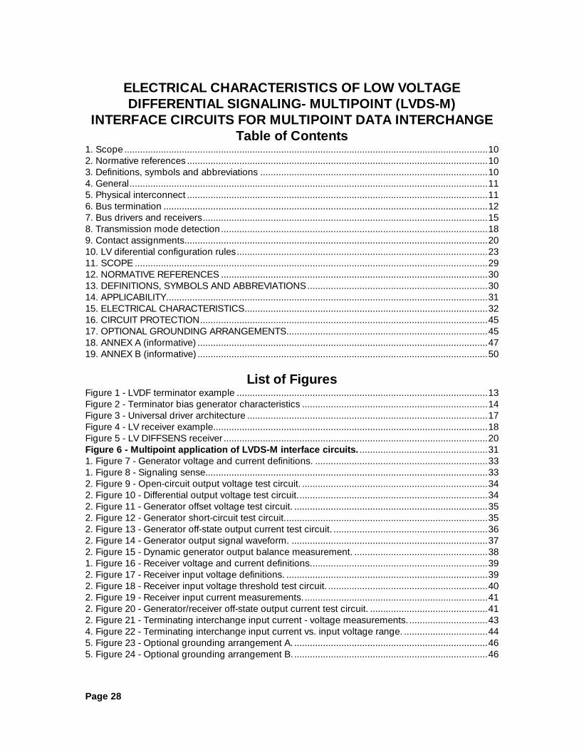
14. APPLICABILITY
14.1 General applicability
The provisions of this Standard may be applied to the circuits employed at the interface betweenequipments where information being conveyed is in the form of binary signals.This Standard specifies the electrical characteristics of the interchange points marked A and B, A'and B', or A/A' and B/B' figure 1.
G R G/R
RtRt
A
B
A'
B'
A/A'
B/B'
L
C C/C'C'
BalancedInterconnecting MediaC - Signal common
G - GeneratorG/R - Combination Generator andReceiverL - Length of stubR - ReceiverRt - Termination resistance
Figure 6 - Multipoint application of LVDS-M interface circuits.The LVDS-M interface is intended for use where any of the following conditions prevail:a. The data signaling rate is too great for effective unbalanced (single-ended) operation.b. The data signaling rate exceeds the capability of TIA/EIA-422-B, EIA-485, or TIA/EIA-612balanced (differential) electrical interfaces.c. The balanced interconnecting media is exposed to extraneous noise sources that may cause anunwanted voltage up to ±1 V measured between the signal conductor and circuit common of agenerator or receiver.d. It is necessary to minimize electromagnetic emissions and interference with other signals.e. Logical inversion of the signals may be required; e.g., a True signal can be changed from ahigh-level to a low-level by exchanging the A and B connections to the balanced interconnectingmedia.
14.2 Data signaling rate
The LVDS-M interface circuit will normally be utilized on data and timing, or control circuits wherethe data signaling rate is up to a recommended maximum limit of 655 Mbit/s. This limit isdetermined by the generator transition time characteristics, the media characteristics, and thedistance between the generator and the load. Certain applications may impose a different (loweror higher) limit for the maximum data signaling rate. This may be accomplished by specifying adifferent minimum generator transition time specification, a different percentage of transition time

Page 32
vs. unit interval at the load, or by a different assumption of the maximum balanced interconnectingmedia signal distortion which is length dependent.The theoretical maximum limit is calculated at 1.923 Gbit/s, and is derived from a calculation ofsignal transition time at the load assuming a loss-less balanced interconnecting media. Therecommended signal transition time (tr or tf) at the load should not exceed 0.5 of the unit intervalto preserve signal quality. This Standard specifies that the transition time of the generator into atest load be 260 ps or slower. Therefore, with the fastest generator transition time, and a loss-lessbalanced interconnecting media, and applying the 0.5 restriction, yields a minimum unit interval of520 ps or 1.923 Gbit/s theoretical maximum data signaling rate.NOTES1 - 655 Mbit/s is the maximum data signaling rate for a serial channel, and employing a parallelbus structure (4, 8, 16, 32, etc. - bus width) can easily extend the obtainable equivalent bit rateinto the Gbit/s range.2 - The recommended maximum data signaling rate is derived from a calculation of signaltransition time at the load. For example, if a cable media is selected, a maximum signal rise timedegradation is assumed to be 500 ps, since cables are not loss-less (500 ps represents a typicalamount of rise time distortion on 5 meters of cable media). Therefore, allowing a 500 psdegradation of the signal in the interconnecting cable yields a 760 ps (fastest) signal at the load. Therefore, with the fastest generator transition time, and a cable with only 500 ps of signaldegradation (transition time), and applying the 0.5 restriction, yields a minimum unit interval of1.520 ns or 655 Mbit/s recommended maximum data signaling rate.Generators and receivers meeting this Standard need not operate over the entire data signalingrate range specified. They may be designed to operate over narrower ranges that satisfy moreeconomically specified applications, for example at lower data signaling rates. When a generatoris limited to a narrower range of data signaling rates, the transition time of the generator may beslowed accordingly to limit noise generation. For example, at 100 Mbit/s the generator's transitiontime should be in the range of 500 ps to 3 ns (5% to 30% of the unit interval), and the signaltransition time at the load should not exceed 5 ns (50% of the unit interval).While a restriction of maximum cable length in not specified, recommendations are given on howto determine the maximum data signaling rate for a typical cable media application (see A.2).
15. ELECTRICAL CHARACTERISTICS
The LVDS-M interface circuit consists of any combination of generators (G), receivers (R), ortransceivers (G/R) totalling thirty-two (32) and a balanced interconnecting media. The followingelectrical characteristics of the interchange connection of these components will allow electricalcompatibility and interchangeability of compliant components.
15.1 Generator characteristics
The fundamental characteristic of a LVDS-M generator is the generation of a first-step differentialoutput voltage of at least 250 mV at the A and B interchange connections to the balanced media.Other charcteristics that affect system performance are the common-mode output voltage, themaximum differential output voltage, the output impedance, and the output signal wave shape.The requirements that follow, define these characteristics in terms of the voltages and currentsdefined in figure 2.
Page 33
G
A
BVB
VA
C
Vt
(VA+VB)/2
IA
IOB
VOS
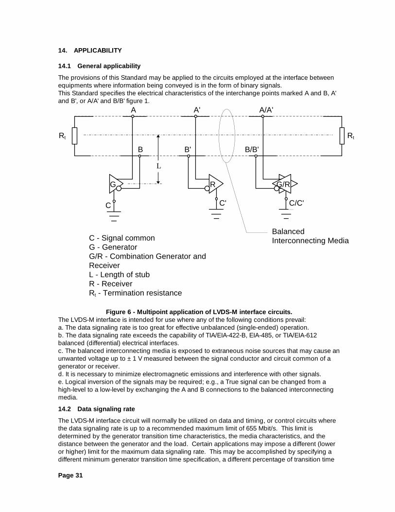
1. Figure 7 - Generator voltage and current definitions.
These requirements are for a generator only. See 5.3 for the characteristics of a combinationGenerator/Receiver (transceiver).The signaling sense of the voltages appearing across the termination resistor is defined in figure 3as follows:a. The A terminal of the generator shall be negative with respect to the B terminal for a binary 1 orOFF state.b. The A terminal of the generator shall be positive with respect to the B terminal for a binary 0 orON state.The logic function of the generator and the receiver is beyond the scope of this Standard, andtherefore is not defined.
C
A
B
VA
VB
| VA - VB |
1 OFF
0
ON
1 OFF
+1.2 V typical
0V (Diff.)
+250 to +400 mV
-250 to -400 mV
ZT = 100 žG
1. Figure 8 - Signaling sense.
15.1.1 Open-circuit output voltages, VOA and VOB
To limit the maximum steady-state voltages at any interchange on the LVDS-M bus, the generatoroutput voltage must be restricted. The highest output voltage occurs with no output current.The voltage between each output terminal of the generator circuit and its common shall bebetween 0 V and 2.5 V when measured in accordance with figure 4. This requirement shall be metin all binary or Off states.0 V < VA < 2.5 V and 0 V < VB < 2.5 V
60Ω

Page 34
1.
G
A
B
Measuredparameter
1, 0, or Off
VOA
VOB
CRL > 1 MΩ2 places
2. Figure 9 - Open-circuit output voltage test circuit.
15.1.2 Differential output voltage, Vt
To assure sufficient voltage to define a valid logic state at any interchange on a fully loaded LVDS-M bus in the presence of a ground potential difference, a minimum differential ouput voltage mustbe generated. This value must be large enough that, after attenuation and allowance for differentialnoise coupling, there is at least +100 mV across the interchange points. A minimum of +250 mVat the generator interchange allows for a loss of 125 mV of signal amplitude or 6 dB of attenuation.There must also be an upper limit to the differential output voltage to define the maximum voltagethat can be attained at an interchange. A maximum output of 450 mV sets the upper bound. Thismaximum output, in conjunction with the generator common-mode output voltage, allowableground potential difference, and application specific parameters shall maintain a voltage between0 V and 2.5 V between any interchange point and its common.The steady-state magnitude of the differential output voltage (Vt), shall be greater than or equal to250 mV and less than or equal to 450 mV when measured with the test circuit shown in figure 5.For the opposite binary state, the polarity of Vt shall be reversed (Vt*). The steady-statemagnitude of the difference between Vt and Vt* shall be 50 mV or less.250 mV < | Vt | < 450 mV250 mV < | Vt* | < 450 mV| Vt | - | Vt* | < 50 mV
1.
G
A
B
Vt60Ω
1.6kΩ
1.6kΩ VTEST0.125V to2.375V
Measuredparameter
+
-Note: Resistors are + 5%
Steady-state logicinput (1 or 0, Highor Low)
2. Figure 10 - Differential output voltage test circuit.

Page 35
15.1.3 Offset (common-mode output) voltage, VOS
The generator output offset plus ground potential difference plus one-half of the differential outputsignal may appear across an interchange point and its common.The steady-state magnitude of the generator offset voltage (VOS), measured with the test load offigure 6 and the generator circuit common shall be greater than or equal to 1.125 V and less thanor equal to 1.375 V for either binary state. The steady-state magnitude of the difference of Vos forone binary state and Vos* for the opposite binary state shall be 50 mV or less.1.125 V < VOS < 1.375 V1.125 V < VOS * < 1.375 V| VOS | - | VOS * | < 50 mV
1.
G
A
B
27Ω + 1%
27Ω + 1%
Measuredparameter
VOS
+
-
Steady-state logicinput (1 or 0, Highor Low)
2. Figure 11 - Generator offset voltage test circuit.
15.1.4 Short-circuit currents, ISA and ISB
Since a LVDS-M bus allows multiple generators, the possibility of contention requires a restrictionon the power that may be sourced to the interchange. This is accomplished with a maximumallowable current from the generator.With the generator output terminals short-circuited to a variable voltage source, the magnitudes ofthe currents (ISA and ISB) shall not exceed 24.0 mA for either binary state (see figure 7) over a testvoltage range of 0 V to 2.5 V.| ISA | < 24.0 mA| ISB | < 24.0 mA
1.
G
A
BISB
Measuredparameter
Steady-state logicinput (1 or 0, Highor Low)
ISA
C
VTEST
+
-0 V to 2.5 V
2. Figure 12 - Generator short-circuit test circuit.

Page 36
15.1.5 Off-state output currents, IOFFA and IOFFB
A generator which is not transmitting and connected to the LVDS-M bus, must not load the busexcessively. This requires restriction of the steady-state and ac currents that can flow at such aninterchange. Since the ac loading of an interchange is common to all types, this requirement isspecificed under 5.5 System characteristics.With the generator in an Off condition (i.e., not transmitting) and the output terminals short-circuited to a variable voltage source, the steady-state magnitudes of the currents, IOFFA and IOFFB
shall not exceed 20 µA over a test voltage range of 0 V to 2.5 V. (see figure 8)These measurements apply with the generator's power supply in both power-on and power-offconditions.| IOFFA | < 20 µA| IOFFB | < 20 µA
1.
G
A
B IOFFB
Measuredparameter
High impedanceor Off state IOFFA
C
VTEST
+
-0 V to 2.5 V
2. Figure 13 - Generator off-state output current test circuit.
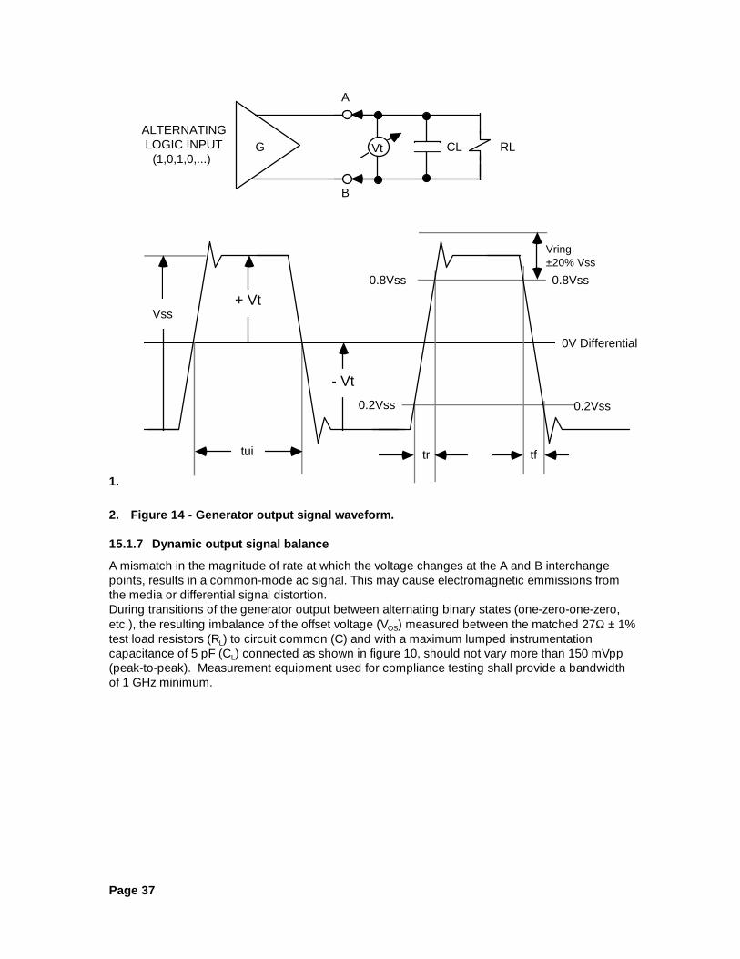
15.1.6 Output signal waveform
The differential output switching or transition time of a generator influences the maximum data rateand maximum stub lengths of a LVDS-M interface. Excessive over and under shoot of the ouputsignal can cause electromagnetic emmissions or false logic state changes on the media.During transitions of the generator output between alternating binary states (one-zero-one-zero,etc.), the differential voltage measured across the 60Ω ± 5% test load (RL) and a maximumlumped instrumentation capacitance of 5 pF (CL), shall be such that the voltage monotonicallychanges between 0.2 and 0.8 of the steady-state output, VSS, and is less than or equal to 0.3 of theunit interval (at the maximum data signaling rate to be employed up to 200 Mbit/s). Above 200Mbit/s the transition time shall be greater than or equal to 260 ps and less than or equal to 1.5 ns. (see figure 9)The signal voltage shall not vary more than ±20% of the steady-state value until the next binarytransition occurs. VSS is defined as the voltage difference between the two steady-state values of the generatoroutput (VSS = 2|Vt|). Measurement equipment used for compliance testing shall provide a bandwidth of 1 GHzminimum.For data signaling rates < 200 Mbit/s ( tui > 5 ns): tr < 0.3 tui, tf < 0.3 tuiFor data signaling rates > 200 Mbit/s and < 655 Mbit/s (1.526 ns < tui < 5 ns):260 ps < tr < 1.5 ns, 260 ps < tf < 1.5 ns
Page 37
1.
Vss
tui
0.2Vss
tr tf
0.2Vss
0.8Vss
0V Differential
G
A
B
Vt
0.8Vss
CL RLALTERNATING LOGIC INPUT
(1,0,1,0,...)
+ Vt
- Vt
Vring ±20% Vss
2. Figure 14 - Generator output signal waveform.
15.1.7 Dynamic output signal balance
A mismatch in the magnitude of rate at which the voltage changes at the A and B interchangepoints, results in a common-mode ac signal. This may cause electromagnetic emmissions fromthe media or differential signal distortion.During transitions of the generator output between alternating binary states (one-zero-one-zero,etc.), the resulting imbalance of the offset voltage (VOS) measured between the matched 27Ω ±1%test load resistors (RL) to circuit common (C) and with a maximum lumped instrumentationcapacitance of 5 pF (CL) connected as shown in figure 10, should not vary more than 150 mVpp(peak-to-peak). Measurement equipment used for compliance testing shall provide a bandwidthof 1 GHz minimum.

Page 38
1.
VosVt
49.9 ž
49.9 ž
Vss
tui
0V Differential
G
A
B
CLALTERNATING LOGIC INPUT
(1,0,1,0,...)
Vos
GND
150 mVp-p
C
A - B
2. Figure 15 - Dynamic generator output balance measurement.
15.2 Receiver characteristics
A receiver indicates the logical state of the LVDS-M bus as defined by the differential voltage thatexists at the interchange. A difference voltage as low as 100 mV defines the state. The receivermust detect this difference over the allowable common-mode input voltage range as determinedby the generator output offset and ground difference voltages.The requirements that follow, define these characteristics in terms of the voltages and currentsdefined in figure 11.
27Ω + 1%
27Ω + 1%
Page 39
R
A'
B'VB'
VA'
C'
VID
(VA'+VB')/2
IA'
IOB'
VCM
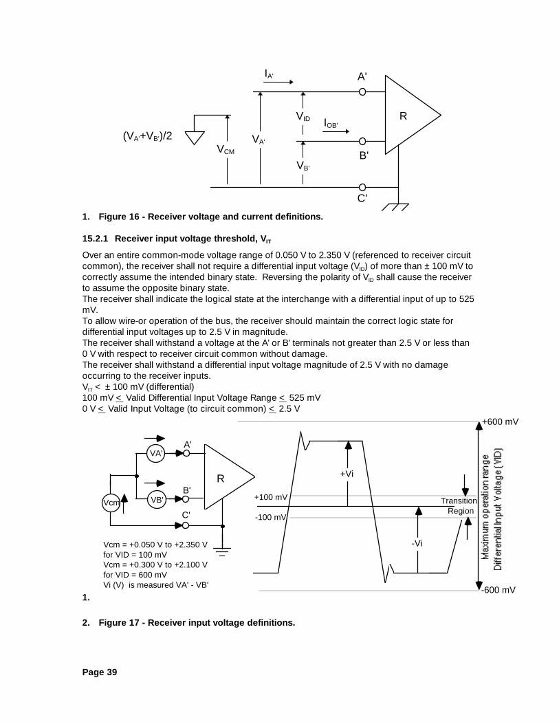
1. Figure 16 - Receiver voltage and current definitions.
15.2.1 Receiver input voltage threshold, VIT
Over an entire common-mode voltage range of 0.050 V to 2.350 V (referenced to receiver circuitcommon), the receiver shall not require a differential input voltage (VID) of more than ±100 mV tocorrectly assume the intended binary state. Reversing the polarity of VID shall cause the receiverto assume the opposite binary state. The receiver shall indicate the logical state at the interchange with a differential input of up to 525mV.To allow wire-or operation of the bus, the receiver should maintain the correct logic state fordifferential input voltages up to 2.5 V in magnitude.The receiver shall withstand a voltage at the A' or B' terminals not greater than 2.5 V or less than0 V with respect to receiver circuit common without damage.The receiver shall withstand a differential input voltage magnitude of 2.5 V with no damageoccurring to the receiver inputs.VIT < ±100 mV (differential)100 mV < Valid Differential Input Voltage Range < 525 mV0 V < Valid Input Voltage (to circuit common) < 2.5 V
1.
R
A'
B'
C'
VA'
VB'Vcm
Vcm = +0.050 V to +2.350 V for VID = 100 mV Vcm = +0.300 V to +2.100 V for VID = 600 mV Vi (V) is measured VA' - VB'
+600 mV
-600 mV
Transition Region
+100 mV
-100 mV
-Vi
+Vi
2. Figure 17 - Receiver input voltage definitions.

Page 40
Table 1 lists the minimum and maximum operating voltages of the receiver (input voltage,differential input voltage, and common-mode input voltage), and the test circuit is shown in figure13. NOTE 7 - The logic function of the receiver is not defined by this Standard.1. Table 10 - Receiver minimum and maximum input voltages.
Applied Voltages(Input Voltage - referenced
to circuit common - C')
ResultingDifferential Input
Voltage
ResultingCommon ModeInput Voltage
Reasonof Test
Via VibVID VCM
+1.250 V +1.150 V +100 mV +1.200 V To guarantee+1.150 V +1.250 V -100 mV +1.200 V operation+2.400 V +2.300 V +100 mV +2.350 V with minimum+2.300 V +2.400 V -100 mV +2.350 V VID applied+0.100 V 0 V +100 mV +0.050 V versus VCM
0 V +0.100 V -100 mV +0.050 V range+1.500 V +0.900 V +600 mV +1.200 V To guarantee+0.900 V +1.500 V -600 mV +1.200 V operation+2.400 V +1.800 V +600 mV +2.100 V with maximum+1.800 V +2.400 V -600 mV +2.100 V VID applied+0.600 V 0 V +600 mV +0.300 V versus VCM
0 V +0.600 V -600 mV +0.300 V range
1.
R
A'
B'
C'
VidVia
Vib Note: Vcm = (Via + Vib)/2, Vid = |Via - Vib|
= Measured Parameter = Applied Voltage
2. Figure 18 - Receiver input voltage threshold test circuit.
15.2.2 Receiver input currents, Iia and Iib
As with a generator, a receiver must not load the bus excessively. Since the ac loading of aninterchange is common to all types, this requirement is specificed under 5.5 Systemcharacteristics.With the voltage ViA (or ViB) ranging from 0 V to +2.4 V while ViB (or ViA) is held at +1.2 V ± 50 mV,the resultant input current IiA (or IiB) shall be no greater than 20 µA in magnitude. Thesemeasurements apply with the receiver's power supply in both power-on and power-off conditions.(see figure 14)| IiA | < 20 µA| IiB | < 20 µA

Page 41
1.
R
A'
B'
C'
Iia
Vib
Via
Iib
= Measured Parameter
2. Figure 19 - Receiver input current measurements.
15.3 Generator/receiver output/input currents, IOFFA/A' and IOFFB/B'
The generator/receiver shall meet the requirements of sections 5.1 and 5.2 when enabledaccordingly. However, the off-state output current of the generator and receiver input currentsshall not be added for the generator/receiver. The load presented to the LVDS-M bus shall complywith the following and 5.5 System characteristics.With the generator/receiver in an Off condition (i.e., not transmitting) and the output terminalsshort-circuited to a variable voltage source, the magnitudes of the currents (IOFFA and IOFFB) shallnot exceed 20 µA over a test voltage range of 0 V to 2.5 V. (see figure 15)These measurements apply with the generator/receiver's power supply in both power-on andpower-off conditions.| IOFFA/A' | < 20 µA| IOFFB/B' | < 20 µA
1.
A
B IOFFB/B'
Measuredparameter
High impedanceor off state IOFFA/A'
C
VTEST
+
-0 V to 2.5 V
G/R
2. Figure 20 - Generator/receiver off-state output current test circuit.
15.4 Interconnecting media electrical characteristics
The balanced interconnecting media shall consist of paired metallic conductors in anyconfiguration which will maintain balanced signal transmission. NOTE 10 - The actual media is not specified and may be: twisted pair cable, twinax cable (parallelpair), flat ribbon cable, or printed-circuit board (PCB) traces.The performance of any balanced interconnecting media used shall be such to maintain thenecessary signal quality for the specific application. If necessary for system consideration,shielding may be employed (see 8.2).

Page 42
Annex A to this Standard provides guidance on performance and cable length versus datasignaling rate and cable recommendations for typical cable applications.
15.4.1 Characteristic impedance
The characteristic impedance of the balanced media shall be 110Ω +/- 20% from 10 MHz to theapplication data rate in Hertz.Note - It is assumed that there are 2 bits transmitted per cycle so that the fundamental frequencyof a data rate of X bps is X/2 Hz.
15.4.2 Attenuation
The attenuation of the output signal from a generator interchange shall be no more than 4.9 dB atany receiving interchange connected to the balanced media. This assures at least 100 mV at anyinterchange with the lowest media chararacteristic impedance and the weakest generator. Thetotal attenuation includes that of the media and the interchange(s).The maximum attenuation requirement shall be met at any frequency up to the application datarate in Hertz.1. Table 11 - Attenuation budget example.
Parameter Derivation ExampleMinimum Output Signal, VOUT Vt/RL x ZO/2 0.25/(60x1.05)x88/2=0.175VMaximum signal loss, Vx VOUT(1-log-1(-4.9/20)) 0.175x(1-0.569)=0.075VMedia Attenuation, Vm VOUT(1-log-1(AL/20)) 0.175xlog-1(0.2x10/20)=0.031VTotal Attenuation for interchangelosses, VAB
Vx - Vm 0.075 - 0.031 = 0.044V
15.4.3 Additional parameters
Additional parameters not specified which are application dependent (see Annex A) are: Maximum Attenuation, Maximum Propagation Delay, Maximum Propagation Delay Skew, Maximum Near End Crosstalk (NEXT), and Maximum Far End Crosstalk (FEXT). Crosstalk, skew,and related pair balance parameters may impact applications with multiple signal transmissionlines.
15.5 System characteristics
15.5.1 Media termination characteristics
All applications shall use a termination impedance at each end of the balanced media. Therecommended value is between 90Ω and 132Ω. The actual value should be selected to match themedia characteristic impedance (+20/-0%) from 10 MHz to the application frequency. Thetermination impedance may be integrated onto the receiver integrated circuit, but subject tomeeting the requirements of 5.5.2 instead of 5.1.5 and 5.2.2.NOTE 8 - Due to the high application frequency, care should be taken in choosing propercomponents such as the termination resistor, and in layout of the printed circuit board. The use ofsurface mount components is highly recommended to minimize parasitic inductance, and leadlength of the termination resistor. Wire wound resistors are not recommended.NOTE 9 - Matching of impedance of the PCB traces, connectors and balanced interconnect mediais highly recommended. Impedance variations along the entire interconnect path should beminimized since they degrade the signal path and may cause reflections of the signal.
15.5.2 Terminating interchanges
As stated earlier, the impedance matching termination may be integrated with the generator,receiver, or generator/receiver. When done, the following interchange requirements supercede the
Page 43
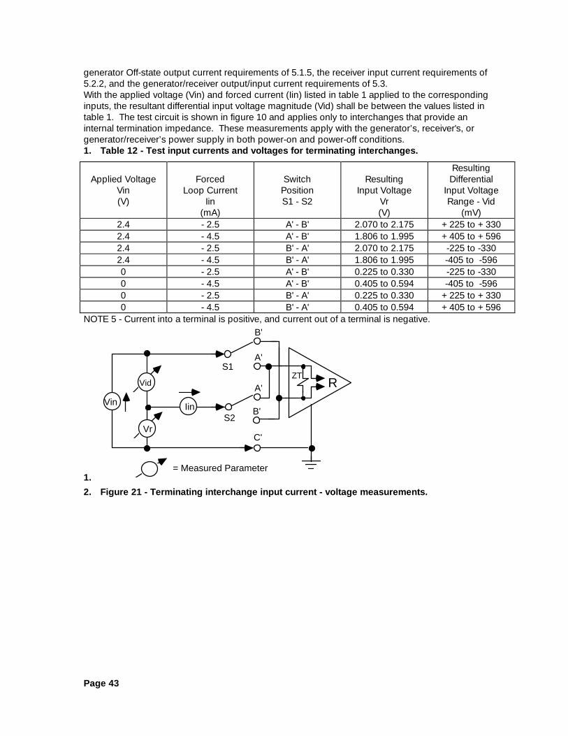
generator Off-state output current requirements of 5.1.5, the receiver input current requirements of5.2.2, and the generator/receiver output/input current requirements of 5.3.With the applied voltage (Vin) and forced current (Iin) listed in table 1 applied to the correspondinginputs, the resultant differential input voltage magnitude (Vid) shall be between the values listed intable 1. The test circuit is shown in figure 10 and applies only to interchanges that provide aninternal termination impedance. These measurements apply with the generator’s, receiver's, orgenerator/receiver’s power supply in both power-on and power-off conditions.1. Table 12 - Test input currents and voltages for terminating interchanges.
Applied VoltageVin(V)
ForcedLoop Current
Iin(mA)
SwitchPositionS1 - S2
ResultingInput Voltage
Vr(V)
ResultingDifferential
Input VoltageRange - Vid
(mV)2.4 - 2.5 A' - B' 2.070 to 2.175 +225 to +3302.4 - 4.5 A' - B' 1.806 to 1.995 +405 to +5962.4 - 2.5 B' - A' 2.070 to 2.175 -225 to -3302.4 - 4.5 B' - A' 1.806 to 1.995 -405 to -5960 - 2.5 A' - B' 0.225 to 0.330 -225 to -3300 - 4.5 A' - B' 0.405 to 0.594 -405 to -5960 - 2.5 B' - A' 0.225 to 0.330 +225 to +3300 - 4.5 B' - A' 0.405 to 0.594 +405 to +596
NOTE 5 - Current into a terminal is positive, and current out of a terminal is negative.
1.
B'
B'
C'
= Measured Parameter
RZT
A'
A'
S1
S2
Vin
Vr
Iin
Vid
2. Figure 21 - Terminating interchange input current - voltage measurements.
Page 44
3.
5004003002001000
2.0
2.5
3.0
3.5
4.0
4.5
132 ž
90 ž
| VID | - Differential Input Voltage - mV
IID -
Lo
op
Cu
rren
t -
mA
600
OPERATING REGION
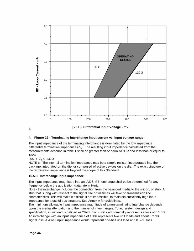
4. Figure 22 - Terminating interchange input current vs. input voltage range.
The input impedance of the terminating interchange is dominated by the low impedancedifferential termination impedance (ZT). The resulting input impedance calculated from themeasurements describe in table 1 shall be greater than or equal to 90Ω and less than or equal to132Ω.90Ω < ZT < 132ΩNOTE 6 - The internal termination impedance may be a simple resistor incorporated into thepackage, integrated on the die, or composed of active devices on the die. The exact structure ofthe termination impedance is beyond the scope of this Standard.
15.5.3 Interchange input impedance
The input impedance magnitude into an LVDS-M interchange shall be be determined for anyfrequency below the application data rate in Hertz.Note - the interchange includes the connection from the balanced media to the silicon, or stub. Astub that is long with respect to the signal rise or fall times will take on transmission linecharacteristics. This will make it difficult, if not impossible, to maintain sufficiently high inputimpedance for a useful bus structure. See Annex A for guidelines.The minimum allowable input impedance magnitude of a non-terminating interchange dependsupon the media attenuation and the number of interchanges. To aid system design andspecification, a unit load is defined as 20kΩ. Each unit load nominally represents a loss of 0.1 dB.An interchange with an input impedance of 10kΩ represents two unit loads and about 0.2 dBsignal loss. A 40kΩ input impedance would represent one-half unit load and 0.5 dB loss.

Page 45
15.5.4 Total load limit
The total number of interchanges to be connected to the LVDS-M bus shall be such that thecombination of unit load and media attenuation is less than 4.9 dB. For example, a 10 m mediawith -0.2 dB/m leaves enough signal for about 29 unit loads.
15.5.5 Failsafe operation
Other standards and specifications using the electrical characteristics of the LVDS-M interfacecircuit may require that specific interchange circuits be made failsafe to certain fault conditions. Such fault conditions may include one or more of the following:1) generator in power-off condition2) receiver not connected with the generator3) open-circuited interconnecting cable4) short-circuited interconnecting cable5) input signal to the load remaining within the transition region (±100 mV) for an abnormalperiod of time (application dependent)When detection of one or more of the above fault conditions is required by specified applications,additional provisions are required in the load and the following items must be determined andspecified:1) which interchange circuits require fault detection2) what faults must be detected3) what action must be taken when a fault is detected; the binary state that the receiver assumes4) what is done does not violate this StandardThe method of detection of fault conditions is beyond the scope of this Standard.
16. CIRCUIT PROTECTION
The LVDS-M interchange, under either the power-on or power-off condition, complying to thisStandard shall not be damaged under the following conditions:a. Generator open circuit.b. Short-circuit across the balanced interconnecting media.c. Short-circuit to circuit common or 2.5 V.NOTE 12 - It is advisable that there be protection from Electrostatic Discharge to the LVDS-Minterchange. The extent of which should be determined and specified by the application.
17. OPTIONAL GROUNDING ARRANGEMENTS
17.1 Signal common (ground)
Proper operation of the LVDS-M interface circuits requires the presence of a signal common pathbetween the circuit commons of the equipment along the media. The signal common interchangelead shall be connected to the circuit common which shall be connected to protective ground byany one of the following methods, shown in figures 18 and 19, as required by specific application.The same configuration need not be used at both ends of an interconnection; however, careshould be exercised to prevent establishment of ground loops carrying high currents.
17.1.1 Configuration "A"
The circuit common of the equipment is connected to protective ground, at one point only, by a100 , ±20%, resistor with a power dissipation rating of 0.5 W. An additional provision may bemade for the resistor to be bypassed with a strap to connect circuit common and protectiveground directly together when specific installation conditions necessitate.NOTE 13 - Under certain ground fault conditions in configuration "A", high ground currents maycause the resistor to fail; therefore, a provision shall be made for inspection and replacement ofthe resistor.

Page 46
1.
GWG
Optional Strap
100 ž 0.5 W
SC
Protective ground or Frame ground
Circuit common or Circuit ground
2. Legend:3. GWG = Green wire ground of power system4. SC = Signal common interchange circuit
5. Figure 23 - Optional grounding arrangement A.
17.1.2 Configuration "B"
The circuit common shall be connected directly to protective ground.
1.
GWG
SC
Protective ground or Frame ground
Circuit common or Circuit ground
2. Legend:3. GWG = Green wire ground of power system4. SC = Signal common interchange circuit
5. Figure 24 - Optional grounding arrangement B.
17.2 Shield ground - cable applications
Some interface applications may require the use of shielded balanced interconnecting media forEMI or other purposes. When employed, the shield shall be connected only to frame ground ateither or both ends depending on the specific application. The means of connection of the shieldand any associated connector are beyond the scope of this Standard.

Page 47
18. ANNEX A (informative)
GUIDELINES FOR CABLE APPLICATION(This annex is not a formal part of the attached TIA/EIA Recommended Standard, but is includedfor information purposes only.)
18.1 Interconnecting cable
The following section provides further information to Section 5.3 and is additional guidanceconcerning operational constraints imposed by the cable media parameters of length andtermination. Generally, if more than one signal transmission line is required for an interface, twisted pairs arenecessary to balance coupling reactance between individual conductors of adjacent pairs andthus reduce crosstalk.
18.1.1 Length
The length of the cable separating the generator and the load is based on a maximum loopresistance of 50 , and a corresponding 125 mV loss of the signal. The following examples given take only the DC effects into account in determining the maximumcable length. This would pertain to low speed operation only. The AC effects will limit themaximum cable length before the DC resistance for high speed applications. See section A.2.For the following cables gauges, the corresponding maximum length for a 50 mV signal loss is:
28 AWG 50 meters (164 feet), 24 AWG 150 meters (492 feet)
Longer lengths are possible, if the voltage attenuation is allowed to decrease the minimumgenerator differential output voltage to the maximum receiver threshold voltage (250 mV to 100mV) for a 150 mV voltage attenuation or -7.9 db. For the following cables gauges, thecorresponding maximum length at a 150 mV signal loss is:
28 AWG 150 meters (492 feet), 24 AWG 450 meters (1,476 feet)
18.1.2 Typical cable characteristics
18.1.2.1 Parallel interface cable
The following characteristics apply to common parallel interface cable (as used for TIA/EIA-613,and other I/O interface standards) consisting of 25 twisted pairs surrounded by an overall shield:
18.1.2.1.1 Parallel cable, physical characteristics
Conductor 28 AWG, 7 strands of 36 AWG, tinned annealed copper, nominal diameter 0.38 mm (0.015 inch)
Insulation Polyethylene or polypropylene; 0.24 mm (0.0095 inch) nominal wall thickness; 0.86 mm (0.034 inch) outside diameter
Foil Shield 0.051 mm (0.002 inch) nominal thickness aluminum / polyester laminated tape helically wrapped around the core
Braid Shield braided 36 AWG, tinned copper with 80% minimum coverage, in electrical contact with the aluminum surface of the foil shield
Diameter nominal overall cable diameter 9.5 mm (0.375 inch)
18.1.2.1.2 Parallel cable, electrical characteristics
DC Resistance 221 / km (67.5 /1000 feet)Mutual Capacitance 43 pF/m (13 pF/ft) at 1 kHzImpedance (characteristic, differential mode) 110 nominal at 50 MHzPropagation Delay 4.8 ns/m (1.46 ns/ft)

Page 48
Attenuation 0.28 dB/m (0.085 dB/ft) at 50 MHzSkew (propagation delay) 0.115 ns/m (0.035 ns/ft)Maximum Crosstalk (Near End, NEXT) 30 dB at 50 MHz
18.1.2.2 Serial interface cable
The following characteristics apply to a common Category 5 serial interface cable (as used forTIA/EIA-422-B, and other I/O interface standards) consisting of 4 unshielded twisted pairssurrounded by an overall jacket:
18.1.2.2.1 Serial cable, physical characteristics
Conductor 24 AWG, 7 strands of 32 AWG, tinned annealed copper, nominal diameter 0.61 mm (0.024 inch)
Insulation Polyethylene or polypropylene; 0.18 mm (0.007 inch) nominal wall thickness; 0.97 mm (0.038 inch) outside diameter
Foil Shield optionalBraid Shield optionalDiameter nominal overall cable diameter 5.6 mm (0.22 inch)
18.1.2.2.2 Serial cable, electrical characteristics
DC Resistance 84.2 / km (25.7 /1000 feet)Mutual Capacitance 48 pF/m (14.5 pF/ft) at 1 kHzImpedance (characteristic, differential mode) 100 nominal at 50 MHzPropagation Delay 4.8 ns/m (1.46 ns/ft)Attenuation 0.17 dB/m (0.051 dB/ft) at 50 MHzMaximum Crosstalk (Near End, NEXT) 36.8 dB at 50 MHz
18.1.3 Cable termination
The characteristic impedance of twisted pair cable is a function of frequency, wire size and type aswell as the kind of insulating materials employed. For example, the characteristic impedance ofaverage 28 AWG, copper conductor, plastic insulated twisted pair cable, to a 50 MHz sine wavewill be on the order of 110 .The range of 90 to 132 allows for a range of media characteristic impedance to be specified. The nominal media characteristic impedance is restricted to the range of 100 to 120 to allowfor impedance variations within the media. Depending upon the balanced interconnecting mediaspecified, the termination impedance should be within 10% of the nominal media characteristicimpedance.
18.2 Cable length vs. data signaling rate guidelines
The maximum permissible length of cable separating the generator and the load is a function ofdata signaling rate and is influenced by the tolerable signal distortion, the amount of longitudinallycoupled noise and common potential differences introduced between the generator and the loadcircuit commons as well as by cable balance. Increasing the physical separation and theinterconnecting cable length between the generator and the load interface points increasesexposure to common mode noise, signal distortion, and the effects of cable imbalance. Accordingly, users are advised to restrict cable length to a minimum, consistent with the generatorto load physical separation requirements.To determine the maximum data signaling rate for a particular cable length the followingcalculations / testing is recommended. First, the maximum DCR of the cable length (loopresistance) should be calculated, then the resulting signal attenuation should be calculated at theload. The voltage at the load must be greater than the receiver thresholds of 100 mV. For aconservative design, a maximum attenuation of 50 mV is recommended. Next eye patterns arerecommended to determine the amount of jitter at the load at the application data signaling rate
Page 49
and comparing that to system requirements. Typically maximum allowable jitters tolerances rangefrom 5% to 20% depending upon actual system requirements. This testing should be done in theactual application if possible, or in a test system that models the actual application as close aspossible. Parameters that should be taken in account include: balanced interconnect mediacharacteristics, termination, protocol and coding scheme, and worst case data patterns (pseudorandom for example). The generator / receiver manufacturers and also the media manufacturersshould provide additional guidance in predicting data signaling rate versus cable length curves fora particular generator / receiver and a particular media as this relationship is very dependent uponthe actual characteristics of the selected devices and media.When generators are supplying symmetrical signals to clock leads, the period of the clock, ratherthan the unit interval of the clock waveform, shall be used to determine the maximum cablelengths (e.g., though the clock rate is twice the data rate, the same maximum cable length limitsapply).
18.3 Co-directional and contra-directional timing information
With co-directional (same direction as data) timing, there are minimal problems with properclocking of the data bits since the difference between data and clock edges is mostly the result ofgenerator and receiver skew and not the transmission line. With contra-directional timing, the user is advised that generator and receiver skew are not theonly items to be taken into account. The cable delay and skew must also be considered.
18.4 In both cases the clock should transition as close to the center of the data bit aspossible.
Page 50
19. ANNEX B (informative)
19.1 Compatibility with other interface standards
The LVDS-M interface circuit is not intended for direct inter-operation with other interface electricalcharacteristics such as TIA/EIA-422-B, EIA-485, TIA/EIA-612, ITU-T (Formerly CCITT)Recommendation V.11, emitter coupled logic (ECL) or PECL.Under certain conditions, inter-operation with circuits of some of the above interfaces may bepossible but may require modification in the interface or within the equipment, or may requirelimitations on certain parameters (such as common mode range); therefore, satisfactory operationis not assured, and additional provisions not specified herein may be required.
19.1.1 Generator output levels (figure B.1)
A generator complying to this Standard features a differential current source capable of delivering a loop current in the range of 2.5 mA to 4.5 mA. When loaded with a 100 load, the resultingdifferential voltage across the resistor will be at least 250 mV and less than 450 mV (Vt). Thecenter point is typically +1.2 V (Vos). These voltages are depicted in figure B.1. Any balanced receiver device that guarantees and input range of at least 0V to +2.4V, andthresholds of 200 mV or less may directly inter-operate with the generator specified by thisStandard and total noise is less than 50 mV. The balanced receiver specified by this Standard may inter-operate with other balancedgenerators specified by other standards along as the balanced generator does not violate themaximum receiver input voltage range, and develops a differential voltage of at least 100 mV, andnot greater than 600 mV. Inter-operation with generators that provide a greater differential voltagemay also be possible with the use of an attenuating circuit. The actual arrangement of suchcircuits is beyond the scope of this annex.
Page 51
1.
Voa
Vob
GND
| Vt |² | Vt |
0 V Differential
Vos² | Vos |
GND
SW
ITC
HIN
G IN
PU
T
SQ
UA
RE
WA
VE
= Measured Parameter
GA
B
VosVt49.9 ž
49.9 ž
C
Voa
Vob
2. Figure B.1 - Generator output levels
19.1.2 Compatibility with IEEE 1596.3
This Standard features very similar DC electrical specifications to the IEEE 1596.3 standard titled:SCI-LVDS-M Low Voltage Differential Signals Specifications and Packet Encoding. Direct inter-operation should be possible at certain data signaling rates without the use of intermediatecircuitry. This Standard specifies generic electrical characteristics of low voltage differentialsignaling interface circuits for general purpose applications.
19.1.3 Compatibility with other interface standards
To determine if direct inter-operation is possible with other interface standards, generator outputlevels, and receiver input specifications must be compared. Specifically the generator's differentialoutput voltage, and offset voltage must be within the bounds of the receiver's input ranges. Correspondingly, the receiver's input thresholds, and input voltage range must be able to acceptthe generator's output levels. If this is the case, direct inter-operation is possible. If differences

Page 52
exists, additional provisions and or precautions may be required. This may include modification oradditional circuitry inserted at the interface points or imposing limitations on certain parameterssuch as maximum common potential difference. The exact circuitry required is beyond the scopeof this annex.
19.2 Power dissipation of generators
Power dissipation is greatly reduced within the generator circuits compared to other differentialstandards which specify a voltage mode generator. The current mode generator can produceless spike current during transitions compared to a voltage mode generator. As data signalingrate increases, this component becomes more critical. This allows for the generator to operateinto the 300 MHz region without the use of special integrated circuit packages or heat sinks. Theload signal is specified between 250 mV and 450 mV typically with a 60Ω load, with creates asmall loop current of only 4 to 8 mA compared to the minimum 20 mA loop current for adifferential TIA/EIA-422-B generator. Since the load current component in also reduced, thisallows for highly integrated generator / receiver devices to be offered in one package or integratedwith other VLSI controller integrated circuits.
19.3 Related TIA/EIA standards
TIA/EIA-422-B Electrical Characteristics of Balanced Voltage Digital Interface CircuitsEIA-485 Standard for Electrical Characteristics of Generators and Receivers for use in BalancedDigital Multipoint SystemsTIA/EIA-612 Electrical Characteristics for an Interface at Data Signaling Rates up to 52 Mbit/s
19.4 Other related interface standards
IEEE 1596.3 SCI-LVDS Low Voltage Differential Signals Specifications and Packet EncodingITU-T (formerly CCITT) Recommendation V.11 Electrical characteristics for balanced double-current interchange circuits for general use with integrated circuit equipment in the field of datacommunications