Welcome to INF4420 Projjgects in Analog and mixed signal CMOS design · Welcome to INF4420...
38
Welcome to INF4420 Projects in Analog and mixed signal CMOS design ! Introduction, T uesday 26th of January, 2010 Snorre Aunet, [email protected] Nanoelectronics Group, Dept. of Informatics Office 3432
Transcript of Welcome to INF4420 Projjgects in Analog and mixed signal CMOS design · Welcome to INF4420...

Welcome to INF4420 Projects in Analog and mixed j gsignal CMOS design !
Introduction, Tuesday 26th of January, 2010t oduct o , uesday 6t o Ja ua y, 0 0
Snorre Aunet, [email protected] Group, Dept. of Informatics
Office 3432

INF4420 – V2010:• sa@luke ~ $ ng sinf4420• fridtjha• rise • Lærere:• majacs• hansoei• haraldsf• ragulant
• Amir Hasanbegovic• Snorre Aunet
• eivinsam• natalkov• nikolahl• kritr• sindrso• mshaugla• geiraby• anderhfanderhf• toreivib• mortenhr• moradi• anhtvanhtv• michaol• kklee
3. februar 2010 2

Outline – Tuesday 20th of January• Practical issues• Learning goals• Design project, tools and methods• Syllabus
V b i f i t d ti t i• Very brief introduction to various circuit building blocks
(sample-and-holds bandgap(sample and holds, bandgap references, switched capacitor circuits, Nyquist- and oversampling data converters, phase-locked loops)
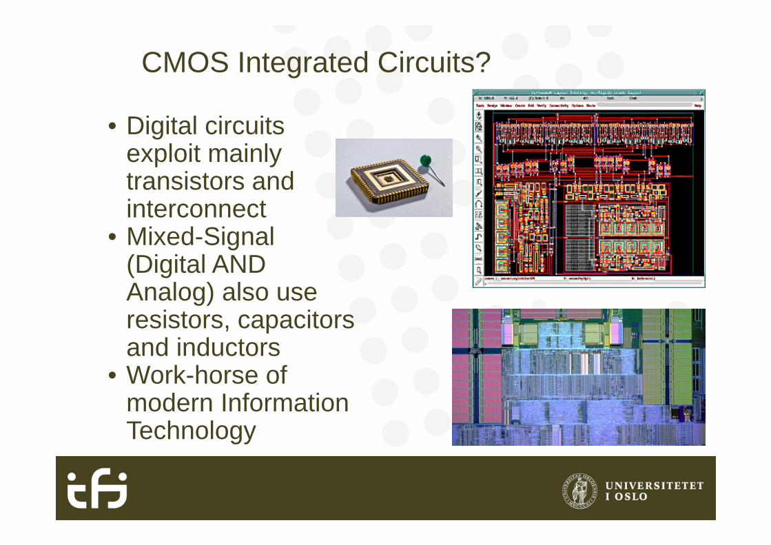
CMOS Integrated Circuits?
• Digital circuits exploit mainlyexploit mainly transistors and interconnectinterconnect
• Mixed-Signal (Digital AND(Digital AND Analog) also use resistors, capacitors and inductors
• Work-horse of d I f timodern Information
Technology

Moore’s law: exponential increase in components per areain components per area
• Challenge to integrate analog and digital (mixed-signal)

http://www.uio.no/studier/emner/matnat/ifi/INF4420/

Why ASICs (Application Specific Integrated Circuits) ??Integrated Circuits) ??
• Advantages:
• Reduced size• Improved performance and functionality• Easier to hide ”company secrets”p y• Reduced cost• Reduced power consumption• Less radiated noise
• Disadvantages:• Increased start-up cost
Hi h d it H t• High power density - Heat• Hard to find top competence• Time consuming development and production• Time to market• Time-to-market

What is an integrated circuit?
• Transistors• Several optionsSeveral options
• Capacitors• How to implement• LinearityLinearity
• Resistors• How to implement• AreaArea
• Inductors• How to implement• Quality factor• Quality factor
• Parasitic components• Calculate• Minimize• Minimize

Design methods; digital from HDL, g gfull custom analog
• Digital systems:Automatic• Automatic synthesis
• VHDL• Schematic
• Analog systems:Analog systems:• Module based• Full-custom

Low Power..
3. februar 2010 10

Mandatory design project
• Design and implement mixed-mode circuit:• Example: ADC, SC-filter, PLL, DAC ( 2008 )• System for automatic removal of mismatch (2009) • Milestones during the process• Milestones during the process• Teaching assistant, Amir Hasanbegovic, will follow
upW it j t t• Write a project report
• LaTeX or similar• Submission: Early/Mid MaySubmission: Early/Mid May• Counts 40 % in the final grading (exam 60%)

Challenge in 2008: Digital-to-Analog Converter (”DAC”)
3. februar 2010 12

INF4420 Project 2009 (1/2)
3. februar 2010 13

INF4420 project 2009 (2/2)
3. februar 2010 14
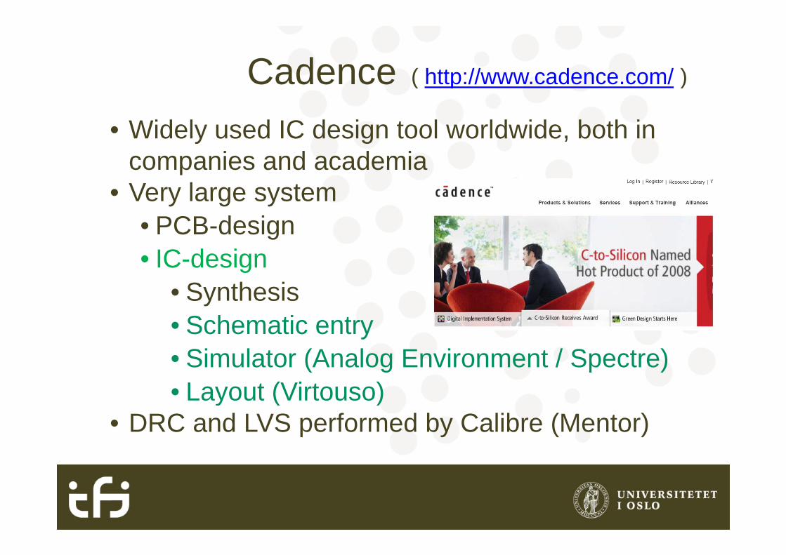
Cadence ( http://www.cadence.com/ ) ( )
• Widely used IC design tool worldwide, both in i d d icompanies and academia
• Very large system• PCB-design• IC-design
• Synthesis• Schematic entry• Simulator (Analog Environment / Spectre)• Layout (Virtouso)y ( )
• DRC and LVS performed by Calibre (Mentor)

Full-custom (”handmade”) design flow
• Design and calculationDesign eq ations• Design equations
• Dimensioning for matching• Schematic entrySchematic entry
• Simulations on cells and top level• Several interactions
• Layout• Module interface• Symmetry/hierarchy• Post Layout Simulations on
iti l d lcritical modules• Next module….

Cadence forts.
S• Start-up:• Web manual
• Standard libraries:• tsmcN90rf • analogLib
• Design views:• Symbol• Schematic• Layout

Schematic entry and simulations in Cadence
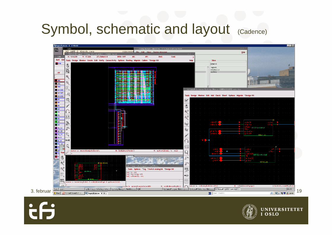
Symbol, schematic and layout (Cadence)
3. februar 2010 19

Process
• TSMC 90 nm low power CMOS:• Minimum gate length: 90nm• 1 Poly-layer1 Poly layer• 9 Metal-layersTrue triple well• True triple well
• Three different threshold voltages• Supply voltage: 1.2 V typ.• Very advanced processVery advanced process

AND-gate
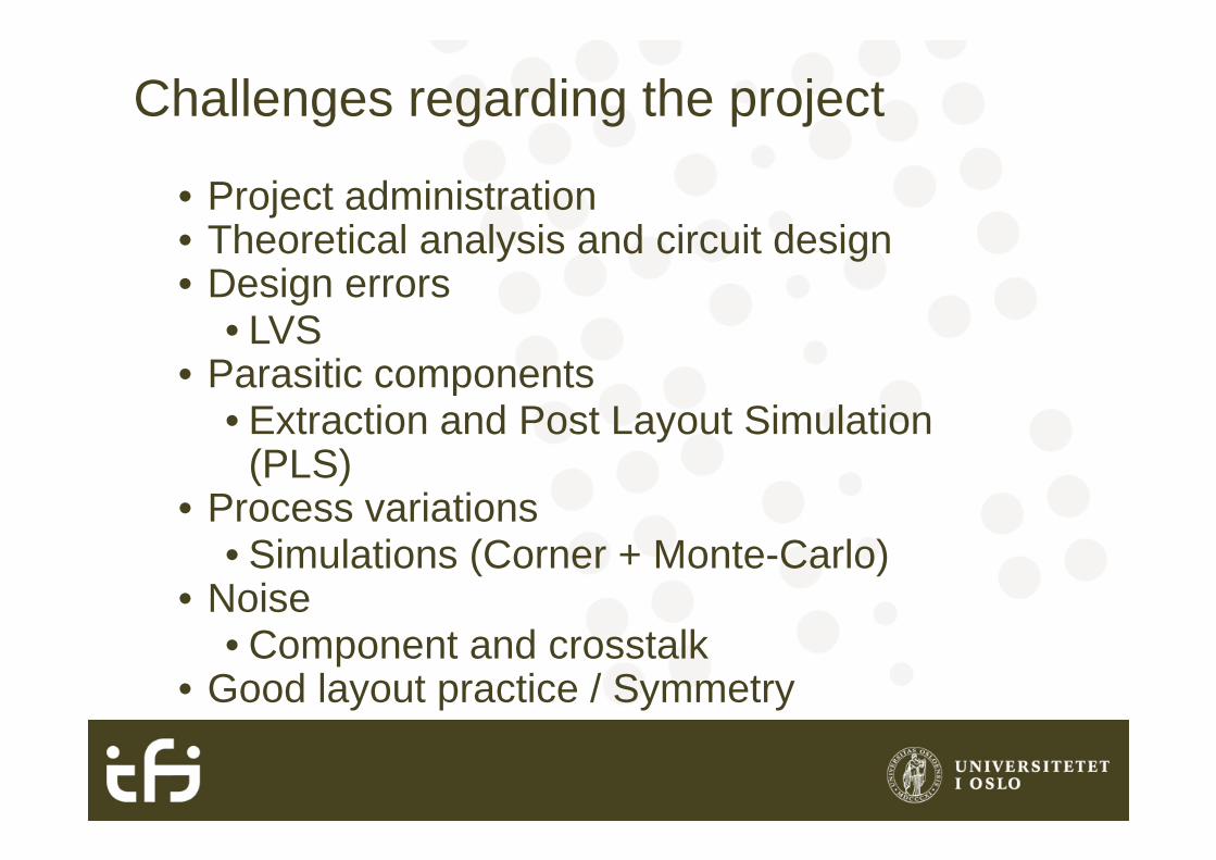
Challenges regarding the project
• Project administration• Theoretical analysis and circuit design• Theoretical analysis and circuit design• Design errors
• LVS• LVS • Parasitic components
• Extraction and Post Layout SimulationExtraction and Post Layout Simulation (PLS)
• Process variations• Simulations (Corner + Monte-Carlo)
• Noise• Component and crosstalk
• Good layout practice / Symmetry
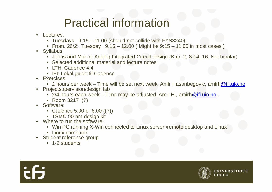
Practical information• Lectures:
• Tuesdays . 9.15 – 11.00 (should not collide with FYS3240).• From. 26/2: Tuesday . 9.15 – 12.00 ( Might be 9:15 – 11:00 in most cases )
• Syllabus:Syllabus:• Johns and Martin: Analog Integrated Circuit design (Kap. 2, 8-14, 16. Not bipolar)• Selected additional material and lecture notes• LTH: Cadence 4.4 • IFI: Lokal guide til CadenceIFI: Lokal guide til Cadence
• Exercises• 2 hours per week – Time will be set next week. Amir Hasanbegovic, [email protected]
• Projectsupervision/design lab• 2/4 hours each week – Time may be adjusted. Amir H., [email protected] .2/4 hours each week Time may be adjusted. Amir H., [email protected] .• Room 3217 (?)
• Software:• Cadence 5.00 or 6.00 ((?))• TSMC 90 nm design kitTSMC 90 nm design kit
• Where to run the software:• Win PC running X-Win connected to Linux server /remote desktop and Linux• Linux computer
• Student reference groupg p• 1-2 students
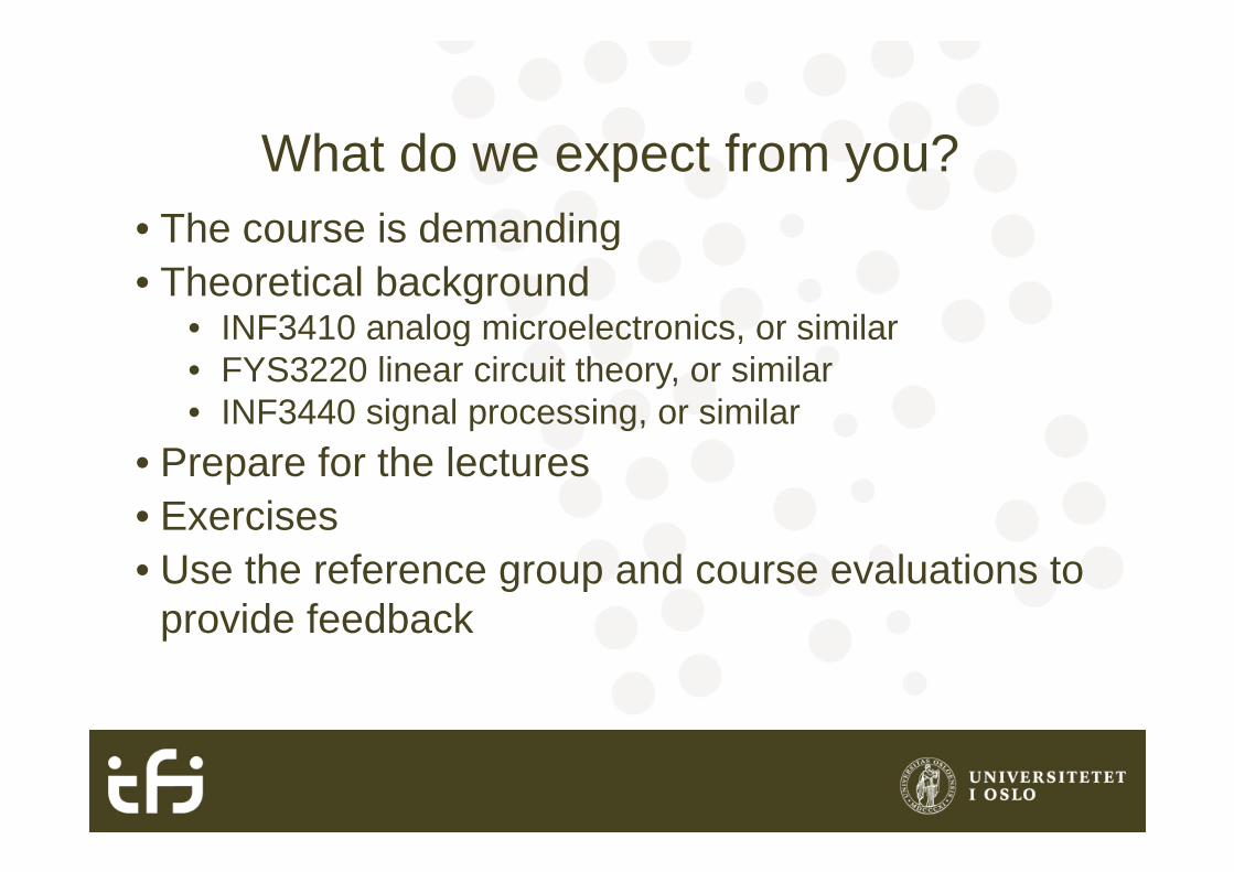
Wh t d t f ?What do we expect from you? • The course is demandingThe course is demanding• Theoretical background
• INF3410 analog microelectronics, or similarINF3410 analog microelectronics, or similar• FYS3220 linear circuit theory, or similar• INF3440 signal processing, or similar
• Prepare for the lectures• Exercises• Use the reference group and course evaluations to
provide feedbackp

Final exam – a few words• Thursday 3rd of June, starting 14:30 (3 hours)
P bl ll l t d t i l f th• Problems usually related to every single of the relevant chapters in the book (2,8,9,…,14,16), and
t i l f th l tmaterial from the lectures
convert to convert to analogx t( )
s t( )
x t( )
x n( ) xc nT( )= y n( ) ys t( ) ysh t( )
y t( )convert todiscrete-time
sequenceDSP
convert toimpulse
trainhold
analoglow-pass
filter
xc t( ) xs t( ) yc t( )
xsh t( ) x n( ) xc nT( )= y n( )ysh t( )
DSPA/D
converter
sample analoglow-pass
filterandhold
D/Aconverterwith hold
xc t( )yc t( )
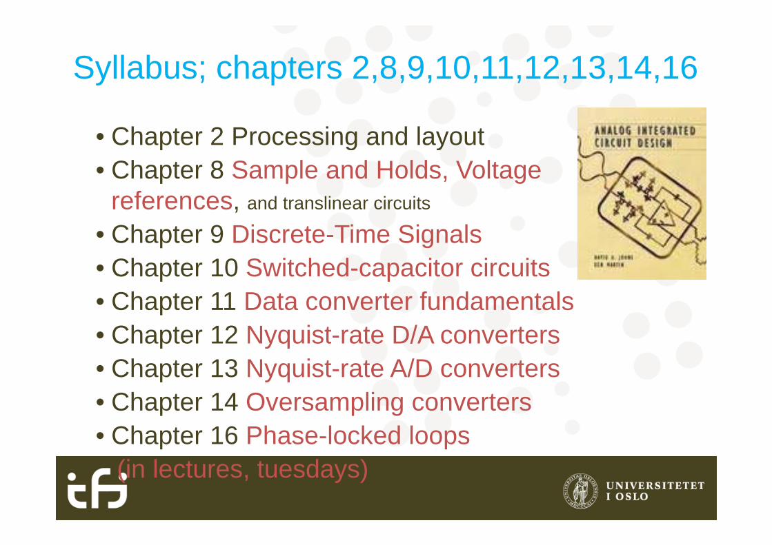
Syllabus; chapters 2,8,9,10,11,12,13,14,16
• Chapter 2 Processing and layoutp g y• Chapter 8 Sample and Holds, Voltage
references, and translinear circuits,• Chapter 9 Discrete-Time Signals• Chapter 10 Switched-capacitor circuitsChapter 10 Switched capacitor circuits• Chapter 11 Data converter fundamentals• Chapter 12 Nyquist rate D/A converters• Chapter 12 Nyquist-rate D/A converters• Chapter 13 Nyquist-rate A/D converters
Ch t 14 O li t• Chapter 14 Oversampling converters• Chapter 16 Phase-locked loops
(in lectures, tuesdays)

Syllabus; chapter 2
• CMOS processing• Relative matching far better than absolute accuracy in CMOS• CMOS layout and design rules• ”Matching is the Achilles heel of analog” C. Diorio, Impinj /
W hi t St t U i itWashington State University• A bad layout can ruin about any analog circuit.

Chapter 8 Sample and Holds, Voltage References
• Performance of S/H• S/H basics• Bandgap voltage reference basics• Circuits for bandgap references g p
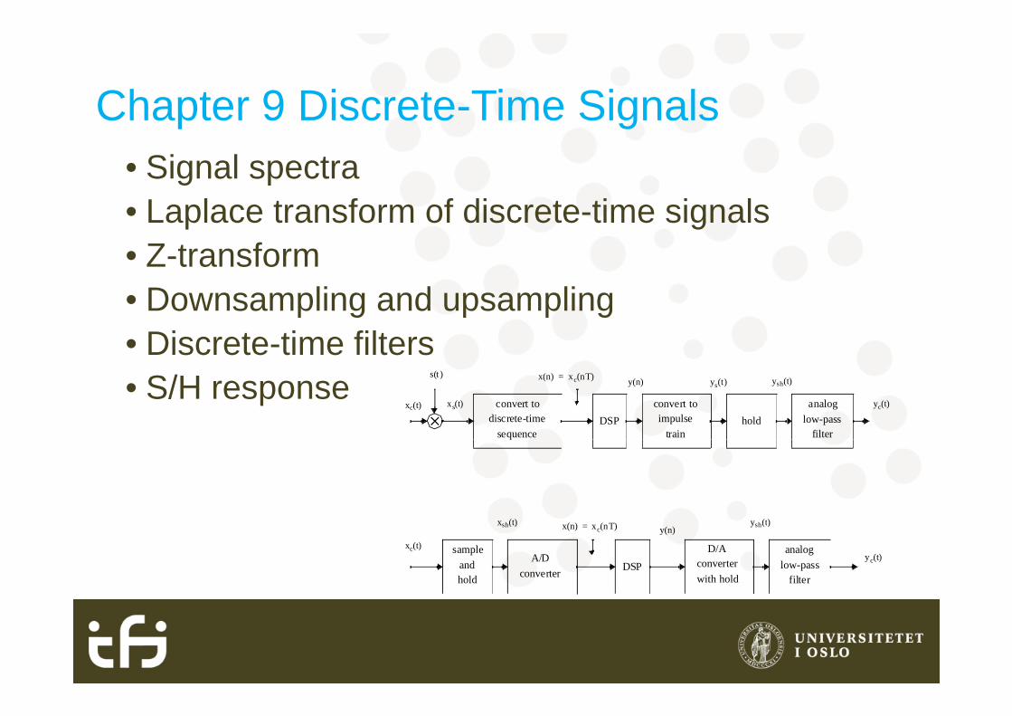
Chapter 9 Discrete-Time SignalsChapter 9 Discrete Time Signals • Signal spectra• Laplace transform of discrete-time signals• Z-transform• Downsampling and upsampling• Discrete-time filters • S/H response
convert todiscrete-time
sequenceDSP
convert toimpulse
trainhold
analoglow-pass
filter
xc t( )
s t( )
xs t( )
x n( ) xc nT( )= y n( ) ys t( ) ysh t( )
yc t( )
q
t( ) t( )
DSPA/D
converter
sample analoglow-pass
filterandhold
D/Aconverterwith hold
xc t( )
xsh t( ) x n( ) xc nT( )= y n( )ysh t( )
yc t( )

Chapter 10 Switched-Capacitor CircuitsChapter 10 Switched Capacitor Circuits • Building blocks• Operation and analysis• First-order filters 21
C2 v t( )
vc2
nT( )
• Biquad filters2
C1
1
vc i
t( )
vcx
t( )
vc o
t( )
vc1
t( )
21 Re q
vo
n( ) vc o
nT( )=vi
n( ) vc i
nT( )=
C1
V1 V2V1 V2
q
Req
TC
1------=
Q C1
V1
V2– every clock period=

Chapter 11 Data converter fundamentalsChapter 11 Data converter fundamentals • Ideal D/A and A/D• Quantization noise• Signed codes• Performance limitations

Chapter 12 Nyquist-Rate D/A ConvertersChapter 12 Nyquist Rate D/A Converters • Decoder-based converters• Binary-scaled converters• Thermometer-code converters• Hybrid conv.
D/ABinVout
in
Vref

Chapter 13 Nyquist-Rate A/D ConvertersChapter 13 Nyquist Rate A/D Converters • Integrating converters
S i t• Successive approx. converters• Algorithmic converters Vref
VinR
• Flash (parallell) conv.• Two-step, interpolating,
Over range
R
V
Vr7
R2----
• Folding, pipelined conv.(2N–1) to N
encoder
N digitaloutputsR
R
R
Vr4
Vr5
Vr6
R
R
R
Vr2
Vr3
Comparators
R Vr1
R 2

Two consequences of the Nyquist-th d ti li i filttheorem and anti-aliasing filters (Wikipedia):
• If the highest frequency B in the original signal is known, the theorem gives th l b d th li f f hi h f t t tithe lower bound on the sampling frequency for which perfect reconstruction can be assured. This lower bound to the sampling frequency, 2B, is called the Nyquist rate.
• If instead the sampling frequency is known, the theorem gives us an upper bound for frequency components, B<fs/2, of the signal to allow for perfect reconstruction. This upper bound is the Nyquist frequency, denoted fN. eco st uct o s uppe bou d s t e yqu st eque cy, de oted
• An anti-aliasing filter is a filter used before a signal sampler, to restrict the bandwidth of a signal to approximately satisfy the sampling theorem. Since the theorem states that unambiguous interpretation of the signal from itsthe theorem states that unambiguous interpretation of the signal from its samples is possible only when the power of frequencies outside the Nyquist bandwidth is zero, the anti-aliasing filter would have to have perfect stop-b d j ti t l t l ti f th th E li bl tiband rejection to completely satisfy the theorem. Every realizable anti-aliasing filter will permit some aliasing to occur; the amount of aliasing that does occur depends on how good the filter is.

Chapter 14 Oversampling Converters
• Oversampling ( >> 2 Nyquist bandwidth) relaxes requirements for matching
• High resolution, low to medium speed• Noise shaping & oversamplingg g• N+1 order modulator gives a certain SNR for
lower OSRthan N-order mod.
• 24 bit Audio conv.24 bit Audio conv.

Chapter 16 Phase-locked loopsChapter 16 Phase locked loops
• Application examples:• clock multiplication,• Freq. generation: The PLL output is a signal with frequency N times
the input frequency where N may be a fractional numberFM demodulation (The input is a FM signal (IF) The output is the• FM demodulation (The input is a FM signal (IF) The output is the demodulated baseband signal
• Products: TV and wireless Phase OutputVinVpd
K
GainLow-pass
filter
H s( )Vlp
detectorp
voltage
Average voltage proportional to phase difference
KlpHlp s( )
VCOVcntl
Vosc(voltage controlled oscillator)

www.akademika.no / www.gnist.no / www.amazon.co.uk
3. februar 2010 37