
UIC NanoEngineering Research Laboratory University of Illinois at Chicago College of Engineering N...
82
UIC NanoEngineering Research Labora University of Illinois at Chicago College of Engineering NanoEngineering Research Lab Applications of Colloidal Quantum Dots and Carbon Nanostructures Michael A. Stroscio a,b,c , and Mitra Dutta a,b Sun Ke, a Milana Vasudev, c Jun Qian, a Sicheng Liao, b Takayuki Yamanaka, a, * D. Ramadurai, c, ** Hye-Son Jung, a Jianyong Yang, a A. Rauchura, a Yang Li, a University of Kentucky, September 24, 2008 a Electrical and Computer Engineering Department, U. of Illinois at Chicago (UIC), 851 S. Morgan Street, Chicago, Illinois 60607 b Physics Department, U. of Illinois at Chicago, 851 S. Morgan Street, Chicago, Illinois 60607 c Bioengineering Department, U. of Illinois at Chicago, 851 S. Morgan Street, Chicago, Illinois 60607 *Now at Northwestern U., M. Razeghi Group, **Now at EPIR, S. Sivananthan
-
Upload
theodore-eaton -
Category
Documents
-
view
217 -
download
1
Transcript of UIC NanoEngineering Research Laboratory University of Illinois at Chicago College of Engineering N...

UIC NanoEngineering Research Laboratory
University of Illinois at Chicago College of Engineering
NNanoEngineeringResearch Lab
Applications of Colloidal Quantum Dots and Carbon Nanostructures
Michael A. Stroscioa,b,c, and Mitra Duttaa,b
Sun Ke,a Milana Vasudev,c Jun Qian,a Sicheng Liao,b Takayuki Yamanaka,a,* D. Ramadurai,c,** Hye-Son Jung,a Jianyong Yang,a A.
Rauchura,a Yang Li,a
University of Kentucky, September 24, 2008
aElectrical and Computer Engineering Department, U. of Illinois at Chicago (UIC), 851 S. Morgan Street, Chicago, Illinois 60607
bPhysics Department, U. of Illinois at Chicago, 851 S. Morgan Street, Chicago, Illinois 60607
cBioengineering Department, U. of Illinois at Chicago, 851 S. Morgan Street, Chicago, Illinois 60607
*Now at Northwestern U., M. Razeghi Group, **Now at EPIR, S. Sivananthan

UIC NanoEngineering Research Laboratory
University of Illinois at Chicago College of Engineering
NNano EngineeringResearch Laboratory
Integrating Nanostructures with Biomolecules: Tool for Studying Biomolecular Architectures
Capabilities for Integrating Nanostructures with Biomolecule
- Synthesis of Biomolecule-Nanostructure Complexes
- Nanostructures used --- CNTs and Quantum Dots (QDs in our arsenal --- Au, CdS, CdSe, CdSe-ZnS, CdTe, ZnO, PbSe, and TiO2)
- Biomolecules studies in our lab by linking with manmade nanostructures include a wide variety peptides (CGGGLDV, CGGGIKVAV, CGGGRGD, CGGGRGDS, CGGGDGEA, GRKKRRQRRR (TAT), CGGGRVDS, GGGC, and many more) and a large variety of single- and double-stranded DNA molecules including ---molecular beacons, short sequences such as TTTTTT, molecular junctions, and specialized sequences such as:Sequence # 1: 5'-Carboxy dT GTATGATATGTTCCCTGGCTCTACTACTGGAGT -3'Sequence # 2: 5'- ACTCCAGTAGAGCCTGGGAA -3'Second sequence (20 bases) is complementary to the first one (30 bases) from 3‘ end.WE WILL MAKE THESE CAPABILITIES AND OTHERS AVAILABLE
TO MEMBERS OF THE BIOMOLECULAR ARCHITECTURE TEAM
Biomolecule
Biomolecules
Biomolecules

UIC NanoEngineering Research Laboratory
University of Illinois at Chicago College of Engineering
NNano EngineeringResearch Laboratory
Integrating Nanostructures with Biomolecules: Relevances tp Biomolecular Architectures
Essential for understanding how environmental effect modify the vibrational, optical, and electronic properties of biomolecules - as an example vibrational modes are modified at boundaries between biomolecules and surfaces in contact with biomolecules (for optical modes boundary conditions such as electrostatic boundary conditions apply and for acoustic modes continuity of displacements and/or normal components of stress tensors) Integrating nanostructures and biomolecules makes it possible to assemble
arrays of structures --- possible coherence enhancements in scattering signatures Our past work has exploited biomolecules to make ordered arrays of man-made nanostructures --- alternatively, nanostructures may be used to make arrays of biomolecules (possible enhancements of scattering signatures) New
CdS CdSe-ZnS-GGGCCdSe-ZnS
Au wire
WE WILL MAKE THESE CAPABILITIES AND OTHERS AVAILABLE TO MEMBERS OF THE BIOMOLECULAR ARCHITECTURE TEAM
Background

UIC NanoEngineering Research Laboratory
Schematic representation of PMMA slides modified chemically to have –NH2 end groups and the DNA strands are attached via glutaraldehyde
Glutaraldehyde, cross-linker
PMMA substrate modified with –NH2 group
NH2 NH2 NH2 NH2 NH2 NH2 NH2 NH2 NH2
DNA strand
NH2 NH2 NH2 NH2NH2 NH2 NH2 NH2 NH2
TiO2 Nanoparticles
Schematic of Immobilized DNA

UIC NanoEngineering Research Laboratory
Schematic of the DNA chemically bound to the PMMA sheets
Glutaraldehyde, cross-linker
PMMA substrate modified with –NH2 group
DNA strand
NH2 NH2 NH2 NH2 NH2 NH2 NH2 NH2 NH2
N N N N N N N N N
AC
TC
GA
GT
AC
AG
CG
AC
CC
AA
CA
TG
AG
AG
AA
C
AC
TC
GA
GT
AC
AG
CG
AC
CC
AA
CA
TG
AG
AG
AA
C
AC
TC
GA
GT
AC
AG
CG
AC
CC
AA
CA
TG
AG
AG
AA
C
AC
TC
GA
GT
AC
AG
CG
AC
CC
AA
CA
TG
AG
AG
AA
C
AC
TC
GA
GT
AC
AG
CG
AC
CC
AA
CA
TG
AG
AG
AA
C
AC
TC
GA
GT
AC
AG
CG
AC
CC
AA
CA
TG
AG
AG
AA
C
AC
TC
GA
GT
AC
AG
CG
AC
CC
AA
CA
TG
AG
AG
AA
C
AC
TC
GA
GT
AC
AG
CG
AC
CC
AA
CA
TG
AG
AG
AA
C
AC
TC
GA
GT
AC
AG
CG
AC
CC
AA
CA
TG
AG
AG
AA
C
AC
TC
GA
GT
AC
AG
CG
AC
CC
AA
CA
TG
AG
AG
AA
C
AC
TC
GA
GT
AC
AG
CG
AC
CC
AA
CA
TG
AG
AG
AA
C
AC
TC
GA
GT
AC
AG
CG
AC
CC
AA
CA
TG
AG
AG
AA
C
AC
TC
GA
GT
AC
AG
CG
AC
CC
AA
CA
TG
AG
AG
AA
C

UIC NanoEngineering Research Laboratory
Illustration of DNA-based SAM fabricated for U. Va. The DNA strands for the formation of the monolayer on PMMA are: 5’- Amino AC TCG AGT ACA GCG ACC CAA CAT GAG AGA AC-‘3 and3’- TG AGC TCA TGT CGC TGG GTT GTA CTC TCT TG carboxy Dt-‘5
The DNA strand with the amino modification on the 5’ end is the one attached to the PMMA substrate modified by hexamethylene diamine to have a-NH2 group and glutaraldehyde is used as the cross-linking agent.
Carboxyl modified DNA was bound to the TiO2 particles via the dopamine modification. The two DNA strands are complementary to each other so they are hybridized to form a double stranded DNA monolayer.
Glutaraldehyde, cross-linker
PMMA substrate modified with –NH2 group
DNA strand
NH2 NH2 NH2 NH2 NH2 NH2 NH2 NH2 NH2
N N N N N N N N N
AC
TC
GA
GT
AC
AG
CG
AC
CC
AA
CA
TG
AG
AG
AA
C
AC
TC
GA
GT
AC
AG
CG
AC
CC
AA
CA
TG
AG
AG
AA
C
AC
TC
GA
GT
AC
AG
CG
AC
CC
AA
CA
TG
AG
AG
AA
C
AC
TC
GA
GT
AC
AG
CG
AC
CC
AA
CA
TG
AG
AG
AA
C
AC
TC
GA
GT
AC
AG
CG
AC
CC
AA
CA
TG
AG
AG
AA
C
AC
TC
GA
GT
AC
AG
CG
AC
CC
AA
CA
TG
AG
AG
AA
C
AC
TC
GA
GT
AC
AG
CG
AC
CC
AA
CA
TG
AG
AG
AA
C
AC
TC
GA
GT
AC
AG
CG
AC
CC
AA
CA
TG
AG
AG
AA
C
AC
TC
GA
GT
AC
AG
CG
AC
CC
AA
CA
TG
AG
AG
AA
C
AC
TC
GA
GT
AC
AG
CG
AC
CC
AA
CA
TG
AG
AG
AA
C
AC
TC
GA
GT
AC
AG
CG
AC
CC
AA
CA
TG
AG
AG
AA
C
AC
TC
GA
GT
AC
AG
CG
AC
CC
AA
CA
TG
AG
AG
AA
C
AC
TC
GA
GT
AC
AG
CG
AC
CC
AA
CA
TG
AG
AG
AA
C
Yale-UIC Collaboration

UIC NanoEngineering Research Laboratory
1450
1600
1750
1900
2050
2200
400 500 600 700 800 900 1000 1100 1200 1300 1400 1500 1600 1700 1800 1900 2000
814
931
1101
1449
1732
514.5 nm laser Raman from RRC
Slit: 50 μm grating: 1800 gr/mm Time: 60sec
Sample #2: Double-stranded DNA /TiO2 (4.5μm)
Raman spectrum from PMMA sample with double stranded DNA bound to TiO2 nanoparticles
PMMA has its major peaks at 1100, 1430, 1780 cm-1
TiO(2) below 620 cm-1
UIC NanoEngineering Research Laboratory
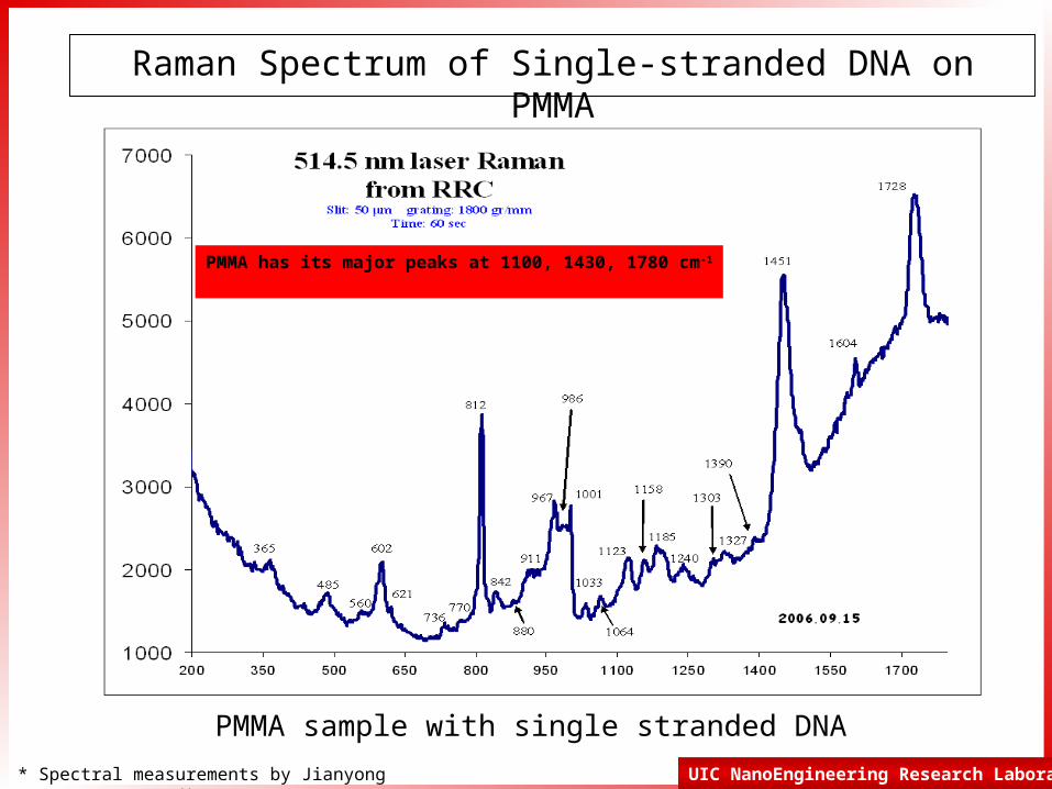
Raman Spectrum of Single-stranded DNA on PMMA
PMMA sample with single stranded DNA
* Spectral measurements by Jianyong Yang
PMMA has its major peaks at 1100, 1430, 1780 cm-1

UIC NanoEngineering Research Laboratory
Raman Spectra were obtained using the Renishaw Raman imaging microscope with an argon ion (514.5 nm) laser and the data is recorded using a CCD camera.
Raman spectra of DNA immobilized on PMMA substrate (a) single stranded amine modified DNA (35 bases) (b). Amine modified GAPDH DNA (850 bp)
Raman Spectroscopy
1250
1500
1750
2000
2250
2500
300 500 700 900 1100 1300 1500 1700 1900
wavelength (cm-1)
Inte
nsi
ty (a
.u.)
563
815
940
1098
1448
1728
A
984
500
700
900
1100
1300
1500
1700
1900
2100
400 600 800 1000 1200 1400 1600 1800 2000
wavelength (cm-1)
Inte
nsity
(a.u
.)
1746
1615
1454
1310
11901075
959
810
835
598560
1240
1110
B

UIC NanoEngineering Research Laboratory
Raman Spectra were obtained using an (325 nm) laser and the data is recorded using a CCD camera.
300
400
500
600
700
800
900
1000
1100
1200
400 600 800 1000 1200 1400 1600 1800 2000
Raman spectra of DNA immobilized on PMMA substrate with a SAM of amine modified GAPDH DNA (850 bp)
Raman Spectroscopy
1000
1500
2000
2500
3000
3500
400 600 800 1000 1200 1400 1600 1800 2000

UIC NanoEngineering Research Laboratory
Raman Spectra were obtained using an (325 nm) laser and the data is recorded using a CCD camera.
500
700
900
1100
1300
1500
1700
1900
2100
400 600 800 1000 1200 1400 1600 1800 2000
rel. (cm-1)
Inte
ns
ity
(a
.u.)
Raman spectra of DNA immobilized on PMMA substrate with a SAM of amine modified GAPDH DNA (850 bp)
Raman Spectroscopy
200
250
300
350
400
450
500
550
600
400 600 800 1000 1200 1400 1600 1800 2000
UIC NanoEngineering Research Laboratory
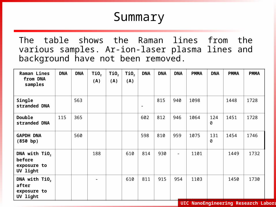
Raman Lines from DNA samples
DNA DNA TiO2
(A)
TiO2
(A)
TiO2
(A)
DNA DNA DNA PMMA DNA PMMA PMMA
Single stranded DNA
563 - 815 940 1098 1448 1728
Double stranded DNA
115 365 602 812 946 1064 1240 1451 1728
GAPDH DNA (850 bp)
560 598 810 959 1075 1310 1454 1746
DNA with TiO2
before exposure to UV light
188 610 814 930 - 1101 1449 1732
DNA with TiO2
after exposure to UV light
- 610 811 915 954 1103 1450 1730
Summary
The table shows the Raman lines from the various samples. Ar-ion-laser plasma lines and background have not been removed.

UIC NanoEngineering Research Laboratory
Molecular beacon
Quantum dotGold NP, quencher
Molecular beacon
Quantum dotGold NP, quencher
Quantum Dot
Molecular Beacon with target DNA strand
Gold NPsGlass substrate
Quantum Dot
Molecular Beacon with target DNA strand
Gold NPsGlass substrate
NNano EngineeringResearch Laboratory
University of Illinois at Chicago College of Engineering
DNA Identification with Molecular Beacons
UIC NanoEngineering Research Laboratory
NNano EngineeringResearch Laboratory
University of Illinois at Chicago College of Engineering
DNA Identification with Molecular Beacons
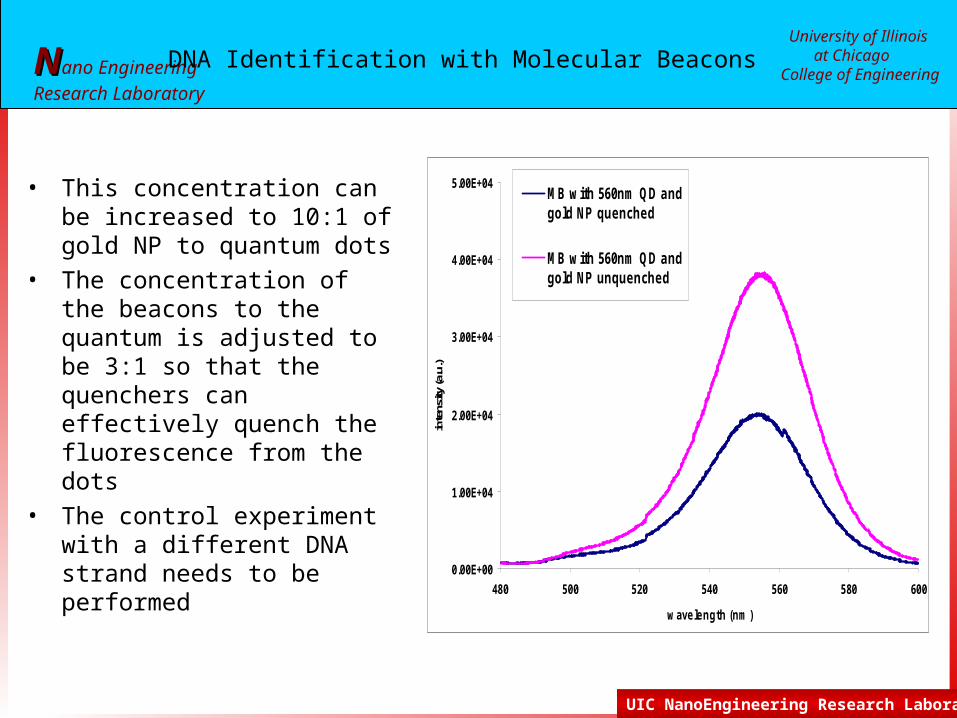
• This concentration can be increased to 10:1 of gold NP to quantum dots
• The concentration of the beacons to the quantum is adjusted to be 3:1 so that the quenchers can effectively quench the fluorescence from the dots
• The control experiment with a different DNA strand needs to be performed
0.00E+00
1.00E+04
2.00E+04
3.00E+04
4.00E+04
5.00E+04
480 500 520 540 560 580 600
w avelength (nm )
inte
nsity
(a.u
.)
MB with 560nm QD andgold NP quenched
MB with 560nm QD andgold NP unquenched

UIC NanoEngineering Research Laboratory
Left-handed Z-DNA is a higher-energy form of the double helix. Each time a right-handed DNA segment turns into Z-DNA, two B–Z junctions form.

UIC NanoEngineering Research Laboratory
I shaped DNA Structure for the study of B-Z DNA transitions
• DNA strands partially complementary to each other are used to form I DNA structure for the study of B-Z transitions.
• When B-Z transition occurs in presence of higher salt concentrations, the quantum dot fluorescence is quenched due to the contact with the quencher, BHQ1; quenching range of the BHQ1 is 480-580 nm
Representation of I DNA structure with the Quantum dot and quencher attached to opposite ends
TCTTGCTCTC TCTTGCTCTC
CACACGAACACACACGAACABHQ1, Quencher
QDAGAACGAGAG
GTGTGCTTGT
GCCG
TCTTGCTCTC TCTTGCTCTC
CACACGAACACACACGAACA BHQ1, Quencher
QDAGAACGAGAG
GTGTGCTTGT
GCCGGC

UIC NanoEngineering Research Laboratory
I shaped DNA Structure for the Study of B-Z DNA Transitions
• DNA strands partially complementary to each other are used to form I DNA structure for the study of B-Z transitions.
• When B-Z transition occurs in presence of higher salt concentrations, the quantum dot fluorescence is quenched due to the contact with the quencher, BHQ1; quenching range of the BHQ1 is 480-580 nm
Representation of I DNA structure with the Quantum dot and quencher attached to opposite ends
TCCTGCTCTCAGGACGAGAG GC CGGTGTGCTTGTCACACGAACA
TiO2QD, Luminescent
Quencher

UIC NanoEngineering Research Laboratory
0.00E +00
2.00E +03
4.00E +03
6.00E +03
8.00E +03
1.00E +04
1.20E +04
1.40E +04
1.60E +04
482 492 502 512 522 532 542 552 562 572
I2.DNA.unquenched
I2.DNA.quenched
I2.DNA.L C .unquenched
I2.DNA.L C .quenched
TCTTGCTCTC--QUENCHERAGAACGAGAG GC CG GCGTGTCGTTGTCACAGCAACA—QD
I-shaped DNA structures with a quencher and a quantum dot (QD) bound to adjacent arms of the structure. The GC-GC-GC linkers undergo pH control- led B- to Z-DNA transitions and move quenchers relative to quantum dots
I. Red Curve in Figure 2; B DNA in cacodylate buffer 50 mM NaCl 2.5 mM MgCl2II. Purple Curve in Figure 2; Z DNA in cacodylate buffer 50 mM NaCl 10 mM MgCl2 0.125 mM Co(NH3)6Cl3III. Green Curve in Figure 2; B DNA in cacodylate buffer 25 mM NaCl 1.0 mM MgCl2IV. Blue Curve in Figure 2; Z DNA in cacodylate buffer 25 mM NaCl 5 mM MgCl2 0.0625 mM Co(NH3)6Cl3

UIC NanoEngineering Research Laboratory
Raman spectra in the region 300-1800 cm-1 of B and Z formsof poly(dG-dC).poly(dG-dC) and their difference spectrum.
Benevides and Thomas, Nucleic Acids Research, 1983

UIC NanoEngineering Research Laboratory
NNano EngineeringResearch Laboratory
University of Illinois at Chicago College of Engineering
Study of DNA Using Indirect Bandgap Semiconductor Quantum Dots
T. Yamanaka, M. Dutta, T. Rajh, and M. A. Stroscio, “Phonon Absorption and Emission by Holes in the HOMO Bands of Duplex DNA,” Proceedings of the International Conference on Hot Carriers in Semiconductors, Proceedings of the International Conference on Hot Carriers in Semiconductors, in Nonequilibrium Carrier Dynamicsin Semiconductors, Springer Proceedings 110, 225-228
(2006). 1D Model for Deformation Potential Scattering of Holes in DNA
• Michael A. Stroscio and Mitra Dutta, “Biologically-inspired Chemically-directed Self-assembly of Semiconductor Quantum-dot-based Systems: Phonon-hole Scattering in DNA Bound to DNA-quantum-dot Complexes,” International Journal of High Speed Electronics, 16(2), 659-668 (2006).• Bykhovskaia, Gelmont, Globus, Woolard et al., Prediction of DNA Far-IR Absorption Spectra based on Normal Mode Analysis, Theor. Chem. Acc., 106, 22 (2001).• Dimitri Alexson, Hongfeng Chen, Michael Cho, Mitra Dutta, Yang Li, Peng Shi, Amit Raichura, Dinakar Ramadurai, Shaunak Parikh, Michael A. Stroscio, and Milana Vasudev, “Semiconductor Nanostructures in Biological Applications,” Journal of Physics: Condensed Matter, 17, R637-R656 (2005)
E
N
m
D
E q
h
1
2
1
2
1
2
1
3
8162
24)(
1
*
2
42
2
2
Experimental Studies of Carrier-Phonon Interactions in DNA
UIC NanoEngineering Research Laboratory
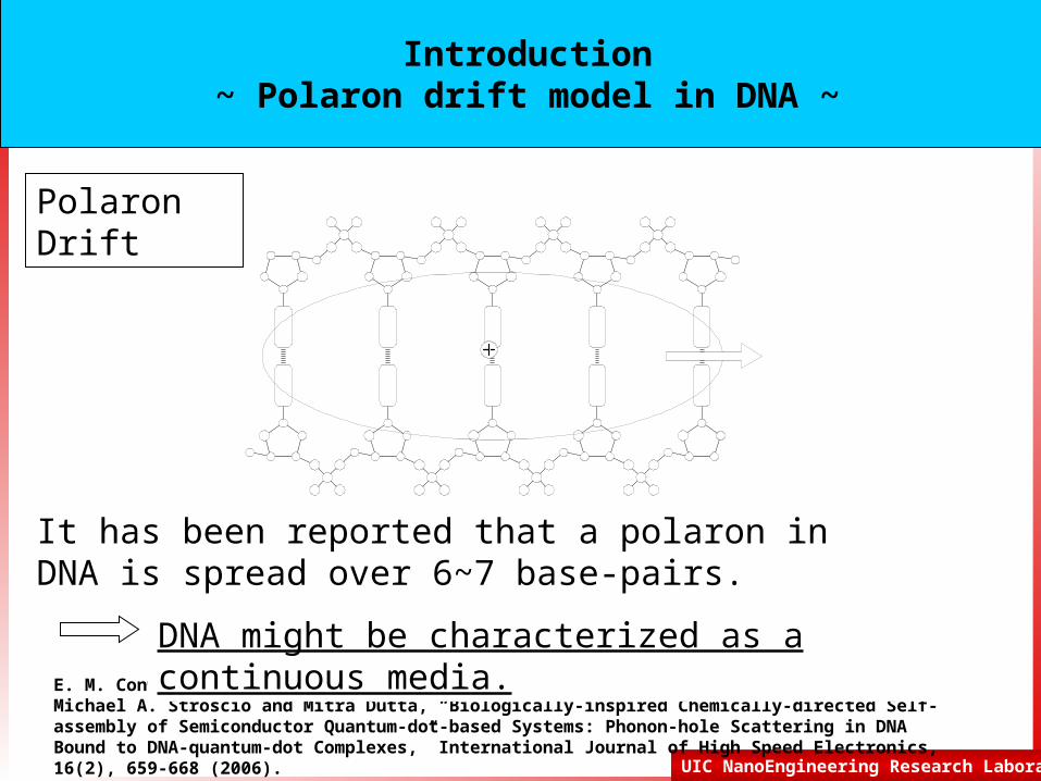
It has been reported that a polaron in DNA is spread over 6~7 base-pairs.
E. M. Conwell and S. V. Rakhmanova, Proc. Natl. Acad. Sci. USA, 97, 4556 (2000); Michael A. Stroscio and Mitra Dutta, “Biologically-inspired Chemically-directed Self-assembly of Semiconductor Quantum-dot-based Systems: Phonon-hole Scattering in DNA Bound to DNA-quantum-dot Complexes,” International Journal of High Speed Electronics, 16(2), 659-668 (2006).
DNA might be characterized as a continuous media.
Polaron Drift
Introduction~ Polaron drift model in DNA ~

UIC NanoEngineering Research Laboratory
Phonon scattering rates are calculated for 1D wire model based on the optical deformation potential.It means
1D quantum wire modelbased on the optical deformation potential
Assumptions
DNA is a 1D chain which consists of base pairs.
All bases have same mass.
The cross section is a rectangle shape.
The elastic constant is identical along the chain.
)(int ruDH op

UIC NanoEngineering Research Laboratory
Phonon-like mode in DNA
Sound velocity along DNA was reported : 1.9 km/sec
This energy looks so small.But, from the basic model of 1D chain
M. B. Hakim, S. M. Lindsay, and J. Powell, Biopolymers., 23, 1185 (1984)
2
at 0s
Cav k
M
If is uniform,
22 = at s
M
vCk
M a a
3.68 meV
Some researchers have reported phonon-like modein the region of ~20 cm-1. For example, Urabe et al. reported 14 cm-1 . 1.74 meV
H. Urabe and Y. Tominaga, Biopolymers., 21, 2477 (1982)
1.74 meV is also a reasonable value.

UIC NanoEngineering Research Laboratory
DNA IP and Semiconductor EvIonization Potential of semiconductor-DNA complexes
-10
-8
-6
-4
-2
0
IP (
eV)
Conduction Band Band GapValence Band 5'GCGTGCGTGGTGC'3
Quantum Dot Interactions with DNA

UIC NanoEngineering Research Laboratory
Energy of carriers [meV]
Em
issi
on r
ate
[sec
-1]
no broadnings= 0.87 meVs= 1.74 meVs= 3.5 meV
(1014)
0 2 4 6 8 10 12
2.0
4.0
6.0
8.0
10.0
12.0
Phonon scattering rates with broadening.
E
N
m
D
E q
1
2
1
2
1
2
1
3
8162
24)(
12
42
2
2
Polaron scattering with the expected longitudinal acoustic phonon mode with a frequency of
14 cm-1 ( = 1.74 meV) evaluated in the Fermi Golden Rule approximation

UIC NanoEngineering Research Laboratory
Scattering Rates for Different Effective Mass
meff = 100 meff = 40 meff = 10 meff = 1
Abs
orpt
ion
rate
[se
c-1]
Carrier energy [meV]0 5 10 15 20
1.0
2.0
3.0(1014)
Em
issi
on r
ate
[sec
-1]
Carrier energy [meV]
meff = 100meff = 40meff = 10meff = 1
0 5 10 15 20
1
2
3
4
(1014)
Absorption Rate Emission RateEphonon = 1.74 meVDop = 0.03x10¹⁰ eV/m = 1.0 meV

UIC NanoEngineering Research Laboratory
Theoretical model
• Characterization of the charge transport in DNA based on phonon scatterings.
• Phonon scattering rates are calculated by the Fermi golden rule and the deformation potential.
• Especially in DNA, phonon scatterings are important on being trapped by an energy valley, typically, G, GG, or GGG site.
Ave
rage
pos
ition
of
char
ges
[nm
]
Time [sec]
Meff = 40
Meff = 60
Meff = 80
Meff = 100
29.2 m/sec
17.5 m/sec
9.29 m/sec
6.84 m/sec
(The electric field : 5.8x10⁵ V/m)
0 0.2 0.4 0.6 0.8 1(10-9)
5
10
15
20
25
The charge movement through DNA starting at position x=0 and illustrates the distance over which
charges are transferred.

UIC NanoEngineering Research Laboratory
Monte Carlo Simulation 1
Simulation of drift
hx
x = 0
V/m108.5 5F
The space is simply one-dimensional without boundaries.
The initial energy is 25.9 meV.
Simulation setup 1

UIC NanoEngineering Research Laboratory
Simulation Result 1
Average position
Eini = 25.9 meVF = 5.8x10⁵ V/mNo boundary
Evaluation ofthe drift velocity
Time [sec]
Ave
rage
pos
ition
of
char
ges
[nm
]
Simulation resultFitted line
meff = 40
meff = 60
meff = 80
meff = 100
29.2 m/sec
17.5 m/sec
9.29 m/sec
6.84 m/sec
0.0 0.2 0.4 0.6 0.8 1.0(10-9)
5
10
15
20
25

UIC NanoEngineering Research Laboratory
Simulation Result 2 (Evaluation of meff)
Saturation velocity due to the effective massEffective mass
Satu
ratio
n ve
loci
ty [
m/s
ec]
0 50 100 150 200
5
10
15
20
25
30
35
40
45
Drift velocity calculated by Conwell is 17.4 m/sec.
meff = 50 ~ 60 is very general value.
S. V. Rakhmanova and E. M. Conwell, J. Phys. Chem. B., 105, 2056 (2001)

UIC NanoEngineering Research Laboratory
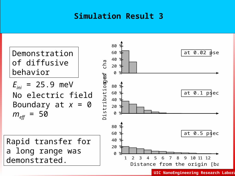
Monte Carlo Simulation 2
Simulation of diffusive behavior
The space is 1D with the boundary at x = 0.
The initial energy is 25.9 meV.
Simulation setup 2
hx
x = 0
No electric field
meff is assumed to be 50.
UIC NanoEngineering Research Laboratory
Simulation Result 3
Demonstration of diffusive behavior
1 2 3 4 5 6 7 8 9 10 11 12
80 %
60 %
40 %
20 %
0 %
80 %
60 %
40 %
20 %
0 %
80 %
60 %
40 %
20 %
0 %
at 0.02 psec
at 0.1 psec
at 0.5 psec
Distance from the origin [base pairs]
Dis
trib
utio
n of
charg
es
Eini = 25.9 meVNo electric fieldBoundary at x = 0meff = 50
Rapid transfer for a long range was demonstrated.
UIC NanoEngineering Research Laboratory
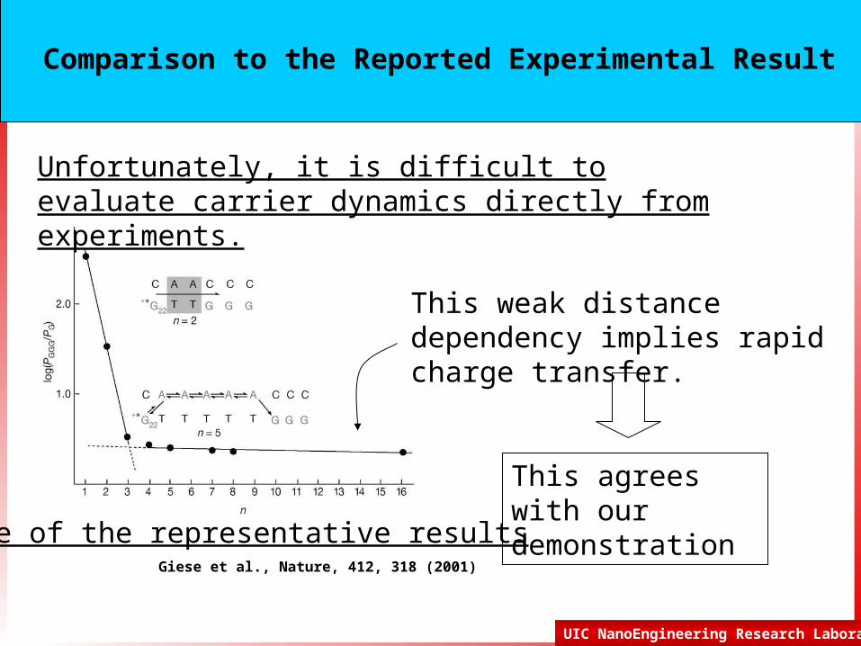
Comparison to the Reported Experimental Result
One of the representative resultsGiese et al., Nature, 412, 318 (2001)
This weak distance dependency implies rapid charge transfer.
Unfortunately, it is difficult to evaluate carrier dynamics directly from experiments.
This agrees with our demonstration

UIC NanoEngineering Research Laboratory
Charge Transfer in DNA
• Charge transfer through DNA via TiO2(titanium dioxide) nanoparticles has been studied in the past.
• TiO2 is a IV-VI semiconductor which has its excitation and emission frequencies in the UV range.
Tijana Rajh et al., J Phys. Chem. B, 2002.
When excited via UV light, TiO2 has excess of holes (charges) which can be transferred to DNA due to the match in their energy levels

UIC NanoEngineering Research Laboratory
Gel Electrophoresis to Detect Cleavage
Lane 1: DNA/TiO2 before illumination with UV light
Lane 2: DNA/TiO2 illuminated with 365 nm UV for 15 min. The Gel clearly shows two separate bands and suggests that cleavage has occurred
Lane 3: Unconjugated DNA oligo (Control). It is evident from the Gel that Lane 1 and 3 have the same molecular weight and hence proves that the TiO2 does not get into the gel and affect the DNA.
Lane 5: 25 bp DNA ladder: 500, 200 125, 75, 50, and 25 bp
1 2 3 5
Nanocomposites used for oligonucleotide cleavage experiments were TiO2/30 sense 5’ Carboxy dT GTATGATATGTTCCCAGGCTCTACTGGAGT and antisense oligo TiO2/30 antisense 5’ ACTCCAGTAGAGCCTGGGAA
5’ COOH TGTATGATATGTTCCCAGGCTCTACTGGAGT AAGGGTCCGAGATDACCTCA 5’

UIC NanoEngineering Research Laboratory
Three-Dimensional DNA Networks
• The three sequences used to form the junction are:
# 1 : 5’-COOH TCTGAGGA
# 2 : 5’ GAGACAGA
# 3 : 5’ TCCTCGTCTC
The TiO2 is attached to the 5’ end of sequence #1.
Should be noted that the three-way junction is a T junction . Two arms are symmetric about the junction
TiO2

UIC NanoEngineering Research Laboratory
Theoretical model
• Characterization of the charge transport in DNA based on phonon scatterings.
• Phonon scattering rates are calculated by the Fermi golden rule and the deformation potential.
• Especially in DNA, phonon scatterings are important on being trapped by an energy valley, typically, G, GG, or GGG site.

UIC NanoEngineering Research Laboratory
u1 = u2 T1normal = T2normal
u = 0 clamped
Tnormal = 0 free-standing
a
M
1M 2M )( 21 MM
a
a '
k
a
M
C4
k
'a
1
2
M
C
2
2
M
C
21
112
MMC
Monoatomic chain Diatomic chain
Dispersion --- monoatomic chain Dispersion --- diatomic chain
k
'a
M
C2
M
C4
k
'a
M
C4
aa
'
2
Dispersion curvefor M1=M2=M
Folding the dispersion curve

UIC NanoEngineering Research Laboratory
DNA is considered as a one-dimensional chain.
If the base sequence is completely random, the number of phonon modes should become a number of base pairs. However, each base pair have almost same mass and it is considered that phonon modes in DNA can be discussed based on a monoatomic chain model.
In monoatomic chains,
at the zone edge.
At the same time, the sound velocity is represented by
at k = 0As a result, the angular frequency becomes
M
C4
M
Cavg
a
vg2

UIC NanoEngineering Research Laboratory
The sound velocity of B-DNA has been measured as 1.9 km/sec [1], and the period of bases is 3.4 Å. Therefore,
3.68 meV corresponds to 29.61 cm-1. This value is the energy of the phonon mode at the zone edge in the case of a uniform one-dimensional chain. However, if the periodic perturbation is assumed with a period of 2a, this energy becomes the energy of the optical mode at the zone center as discussed above. And if the perturbation is more complicated but still weak at the same time, which means that the discussion based on monoatomic chains is still valid, it is expected that another optical modes appear below this energy.
In fact, it has been reported that the lowest lying mode in B-DNA is 14 cm-1 (=1.74 meV) [2]. As a result, it can be said that there is the mode in DNA with only a few meV.
[1] M. B. Hakim, S. M. Lindsay, and J. Powell, ‘The Speed of Sound in DNA’, Biopolymers, 23, pp. 1185-1192, 1984[2] H. Urabe and Y. Tominaga, ‘Low-Lying Collective Modes of DNA Double Helix by Raman Spectroscopy’, Biopolymers, 21, pp. 2477-2481, 1982
[meV] 68.3[rad/sec] 1059.5[rad/sec] 103.4
109.12212
10-
3
a
vg

UIC NanoEngineering Research Laboratory
e-
h+
h+h+
Light
Quantum Dot DNA
TiO2
h+ h+ h+
AuAu
AFM
Glass
TiO2
Au
ssDNA
Measuring I-V Characteristics in ssDNA
Dopamine or 3,4 dihydroxyphenylethylamine
- cd TTTTTT

UIC NanoEngineering Research Laboratory
Au-TiO2-Au without UV Light Au-TiO2-Au with UV Light
e-
h+
h+h+Light
Quantum Dot
TiO2
Au
Au
Current sensing AFM For EF at mid-gap
For FN near Ec
For FP near Ev
I-V Characteristics of Nanostructure Interface

UIC NanoEngineering Research Laboratory
E0 = - 7.4 eVE0 = - 7.0 eV
E0 = - 6.6 eVE0 = - 6.2 eV
I-V Curves for a Au-Ti02-AuEc = - 4.2 eVEv = - 7.4 eV

UIC NanoEngineering Research Laboratory
u1 = u2 T1normal = T2normal
u = 0 clamped
Tnormal = 0 free-standing
a
M
1M 2M )( 21 MM
a
a '
k
a
M
C4
k
'a
1
2
M
C
2
2
M
C
21
112
MMC
Monoatomic chain Diatomic chain
Dispersion --- monoatomic chain Dispersion --- diatomic chain
k
'a
M
C2
M
C4
k
'a
M
C4
aa
'
2
Dispersion curvefor M1=M2=M
Folding the dispersion curve

UIC NanoEngineering Research Laboratory
DNA is considered as a one-dimensional chain.
If the base sequence is completely random, the number of phonon modes should become a number of base pairs. However, each base pair have almost same mass and it is considered that phonon modes in DNA can be discussed based on a monoatomic chain model.
In monoatomic chains,
at the zone edge.
At the same time, the sound velocity is represented by
at k = 0As a result, the angular frequency becomes
M
C4
M
Cavg
a
vg2

UIC NanoEngineering Research Laboratory
The sound velocity of B-DNA has been measured as 1.9 km/sec [1], and the period of bases is 3.4 Å. Therefore,
3.68 meV corresponds to 29.61 cm-1. This value is the energy of the phonon mode at the zone edge in the case of a uniform one-dimensional chain. However, if the periodic perturbation is assumed with a period of 2a, this energy becomes the energy of the optical mode at the zone center as discussed above. And if the perturbation is more complicated but still weak at the same time, which means that the discussion based on monoatomic chains is still valid, it is expected that another optical modes appear below this energy.
In fact, it has been reported that the lowest lying mode in B-DNA is 14 cm-1 (=1.74 meV) [2]. As a result, it can be said that there is the mode in DNA with only a few meV.
[1] M. B. Hakim, S. M. Lindsay, and J. Powell, ‘The Speed of Sound in DNA’, Biopolymers, 23, pp. 1185-1192, 1984[2] H. Urabe and Y. Tominaga, ‘Low-Lying Collective Modes of DNA Double Helix by Raman Spectroscopy’, Biopolymers, 21, pp. 2477-2481, 1982
[meV] 68.3[rad/sec] 1059.5[rad/sec] 103.4
109.12212
10-
3
a
vg

UIC NanoEngineering Research Laboratory
Energy of carriers [meV]
Em
issi
on r
ate
[sec
-1]
no broadnings= 0.87 meVs= 1.74 meVs= 3.5 meV
(1014)
0 2 4 6 8 10 12
2.0
4.0
6.0
8.0
10.0
12.0
Phonon scattering rates with broadening.
E
N
m
D
E q
1
2
1
2
1
2
1
3
8162
24)(
12
42
2
2
Polaron scattering with the expected longitudinal acoustic phonon mode with a frequency of
14 cm-1 ( = 1.74 meV) evaluated in the Fermi Golden Rule approximation

UIC NanoEngineering Research Laboratory
Intrasubband Intersubband
(a) Slab, (b) Reformulated, (c ) Guided, (d) Bulk

UIC NanoEngineering Research Laboratory

UIC NanoEngineering Research Laboratory
UIC NanoEngineering Research Laboratory
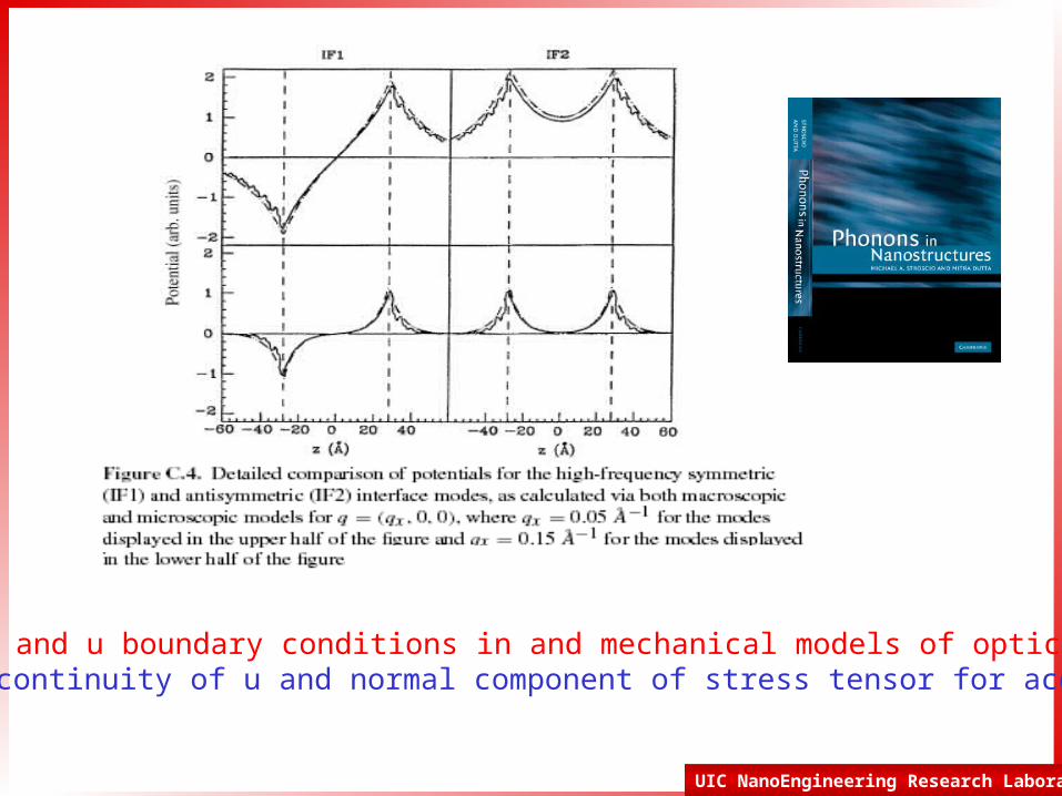
and u boundary conditions in and mechanical models of optical modes, and continuity of u and normal component of stress tensor for acoustic modes

UIC NanoEngineering Research Laboratory
Nano Engineering Research Lab
Univ. of Illinois at Chicago Chicago, USA
Su-Schrieffer-Heeger Hamiltonian
*Sugiyama H. & Saito, I. (1996) J. Am. Chem. Soc. 118, 7063-7068.
M = 4.35 x 10⁻²² g, K = 0.85 eV/A2 (K= Mvsound2/a2), vsound = 1.9 km/s, a = 0.34 nm,
to = 0.36 eV* , determined by interactions of –wavefunctions of adjacent bases* = t/u = 0.6 eV/Angstrom* G = 1.4 eV, A = 0.9 eV, C = .27 eV, T = 0 eV
on-site energy, transfer intergal (to) atthermal equilibrium, change in transfer integral due to displacements = carrier-phonon coupling
potential and kinetic energies ofvibrational modes --- phonons
SSH is used widely to describe polaron transport on polymers

UIC NanoEngineering Research Laboratory
Discussion
• From some of the Raman spectra, we notice that the PMMA has its major peaks at 1100, 1430, 1780 cm-1
• The contribution of the background signal from PMMA is high and may be blocking the weak DNA Raman signatures
• For future experiments– Use longer strands of DNA upto 2K BP obtained from PCR
reactions– Use other methods of tracking double stranded DNA such
as DAPI dye (commonly used biological dye)– Use gel electrophoresis to verify that the exposure to UV
light cleaves the DNA strands bound to TiO2 nanoparticles
UIC NanoEngineering Research Laboratory
Energy transfer between quantum dots and gold nanoparticles
• The transfer of energy is studied between the quantum dots (donors) and gold nanoparticles (acceptors) which leads to quenching of quantum dots
• This energy transfer could be explained as – FRET (fluorescence resonance energy transfer) process and the
efficiency of energy transfer is inversely proportional to d6
– Contact Quenching, which leads to the formation of non-fluorescent complex between the gold nanoparticles and QDs
– SET (Surface energy transfer) where the gold nanoparticles are assumed to behave as a mirror and the efficiency of energy transfer is inversely proportional to d4

UIC NanoEngineering Research Laboratory
• Fort orange dots (605 nm) are conjugated with short peptides (GGGC) using the standard procedures
• Following this, the cysteine group on the peptide is attached to monomaleimido nanogold particles via disulfide bonds
• PL spectra was measured before and after forming the quantum dot/gold nanoparticle complex using the 325 nm Ar+ laser
Procedure

UIC NanoEngineering Research Laboratory
Inte
nsity
(ar
b. U
nits
)
Wavelength in nm
540 565 590 615 640
Wavelength in nm
5000
10000
15000
20000
25000
30000
35000
40000
Inte
nsity
(ar
b. U
nits
)
45000
Backscattering from monomaleimido nanogold particles measured using 325 nm Ar+ Laser
PL spectrum of CdSe-ZnS fort orange quantum dots (E605nm) conjugated with GGGC using 325 nm Ar+ Laser
Emission spectra of Fort orange quantum dots and nanogold particles before forming
complex

UIC NanoEngineering Research Laboratory
Wavelength in nm
Inte
nsity
(ar
b. U
nits
)
Inte
nsity
(ar
b. U
nits
)
Wavelength in nm
PL Spectrum of fort orange quantum dots bound to GGGC and fort orange quantum dots with GGGC in
presence of nanogold particles
PL spectrum of the fort orange dots conjugated with GGGC bound to the monomaleimido nanogold particles
Emission spectra of Fort orange dots and gold nanoparticle complex
UIC NanoEngineering Research Laboratory
FRET and beyond…
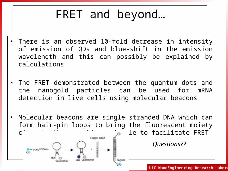
• There is an observed 10-fold decrease in intensity of emission of QDs and blue-shift in the emission wavelength and this can possibly be explained by calculations
• The FRET demonstrated between the quantum dots and the nanogold particles can be used for mRNA detection in live cells using molecular beacons
• Molecular beacons are single stranded DNA which can form hair-pin loops to bring the fluorescent moiety close to the quenching molecule to facilitate FRET
Questions??

UIC NanoEngineering Research Laboratory

UIC NanoEngineering Research Laboratory
Phonon Bottleneck in Carbon Nanotubes
Applications of Short Nanotubes :Applications of Short Nanotubes :
Carbon Nanotube Field Effect Transistors Carbon Nanotube Field Effect Transistors
Field-Emission DisplaysField-Emission Displays
Biomedical SensorsBiomedical Sensors
Light Emitting DiodesLight Emitting Diodes
Molecular ElectronicsMolecular Electronics
Guo and Lundstrom, APL, 86, 193103 (2005)
The role of phonon scattering in carbon nanotube field-effect transistors (CNTFETs) is explored by solving the Boltzmann transport equation using the Monte Carlo method. The results show that elastic scattering in a short-channel CNTFET has a small effect on the source-drain current due to the long elastic mean-free path (mfp) ( 1 μm). If elastic scattering with a short mfp were to exist in a CNTFET, the on current would be severely degraded due to the one-dimensional channel geometry. At high drain bias, optical phonon scattering, which has a much shorter ( 1 μm), is expected to dominate, even in a short-channel CNTFET. Guo and Lundstrom find, however, that inelastic optical scattering has a small effect in CNTFETs under modest gate bias.

UIC NanoEngineering Research Laboratory
Phonon Bottleneck in Carbon Nanotubes
Acoustic Modes in Single Wall Nanotubes (SWNTs)
Amit Raichura, Mitra Dutta, and Michael A. Stroscio, “Continuum Model for Acoustic Phonons and Phonon Bottleneck in Amit Raichura, Mitra Dutta, and Michael A. Stroscio, “Continuum Model for Acoustic Phonons and Phonon Bottleneck in Single Wall Nanotubes,”Single Wall Nanotubes,” J. of Computational ElectronicsJ. of Computational Electronics, Vol. 4, Num 1-2, 91-95; Amit Raichura, Mitra Dutta, and Michael, Vol. 4, Num 1-2, 91-95; Amit Raichura, Mitra Dutta, and MichaelA. Stroscio, “Continuum Model for Acoustic Phonons in Nanotubes: Phonon Bottleneck,”A. Stroscio, “Continuum Model for Acoustic Phonons in Nanotubes: Phonon Bottleneck,” Phys. Stat. Sol.Phys. Stat. Sol. 241; 3448-53241; 3448-53..
Odd Modes:sin sinh cos( )cos( )
2 2
cos cosh sin( )cos( )2 2
cos cosh cos( )cos( )2 2
x
l lu A x k x n t
a a
l lu B x k x n t
a a
l lw C x k x n t
a a
sin2
sinh2
la
kla
tan tanh 02 2
l l
a a
Boundary Conditions
corresponding to 1, 3, 5,… axial half waves = 1.5π, 3.5π, 5.5π,… a
l

UIC NanoEngineering Research Laboratory
Phonon Bottleneck in Carbon Nanotubes
22 2 2 22 2
1 12
2 2 2 2 2 21 2 2
2 1 1
1 12 2
1 1 12 2 2
v vv n n
A
C v v vn n n
2 2 22 1
1 22
2 2 2 2 2 22 1 2
1 2 1
1 12 2
1 1 12 2 2
v vv n n n
B
C v v vn n n
2 2
1
21
lhC
M A BI I
C C
1
2x xu u u u ww dVV M
Amplitude Normalization
4
l
aeI
24cos sin 4 cos2 2 2
l l
a al l lae ka e
a a a
2 32 2 22 2 4 cos
2
l l l l
a a a alk ae le k le ka e
a
322 24 sin 4 sin
2 2
l l
a al l
ka e k a ka ea a
(
)

UIC NanoEngineering Research Laboratory
Phonon Bottleneck in Carbon Nanotubes
0
400
800
1200
1600
0 5 10 15 20
Wav
e N
umbe
r (c
m-1
)
Normalized Wave Vector
Radial
Torsional
Axial
0
200
400
600
800
0 5 10 15 20
Wav
e N
umbe
r (c
m-1
)
Normalized Wave Vector
Radial
Torsional
Axial
(10,10) nanotube with a length of 2.8 nm (10,10) nanotube with a length of 7 nm
Breathing Mode Frequency = 4.93 THz (k = 165 cm-1) Ando et al.., PRB 65, 235412

UIC NanoEngineering Research Laboratory
Phonon Bottleneck in Carbon Nanotubes: Deformation Potential
cos cosh cos2 2
nB l lx k x n
r a a
cos cosh cos2 2
C l lx k x n
r a a
cos cosh cos2 2
A l lu x k x n
a a a
ODD CASE:
EVEN CASE:
sin sinh cos2 2
nB l lx k x n
r a a
sin sinh cos2 2
C l lx k x n
r a a
sin sinh cos2 2
A l lu x k x n
a a a
uD = 24 eVD = 24 eV
HHdefdef = D D
Bardeen AnsatzBardeen AnsatzPRB 65, 235412

UIC NanoEngineering Research Laboratory
Phonon Bottleneck in Carbon Nanotubes --- Energy Subbands (10,0), length = 4 nm
kz = nπ/LL = length of the nanotube
(10,0) tube:Tc = π(2a)/L & T = 0.43 nmL = 9Tkz = nπ/9T
Ref: G. Pennington, PRB 68: 045426
-8
-4
0
4
8
-1 -0.5 0 0.5 1 Tight-Binding Bands Quantizedin Finite-Length NanotubesWave Vector (kz)
En
ergy
(eV
)

UIC NanoEngineering Research Laboratory
Phonon Bottleneck in Carbon Nanotubes: Phonon Assisted Electron Transitions
Axial Phonon at 55 meV
Intravalley Intersubband 2 1 n=1
-6
-3
0
3
6
-1 -0.5 0 0.5 1
Wave Vector (kz)
En
ergy
(eV
)

UIC NanoEngineering Research Laboratory
Phonon Bottleneck in Carbon Nanotubes: Phonon Assisted Electron Transitions
-8
-4
0
4
8
-1 -0.5 0 0.5 1
Intravalley Intersubband 3 1 n=1
Torsional Phonon at 37 meV
Wave Vector (kz)
En
ergy
(eV
)

UIC NanoEngineering Research Laboratory
Close-packed PbSe colloidal quantum dots
6.4 nm
weaker coupling
stronger coupling
Au
Au
Si3
N4
1.0 nm
2.3 nm
M.D. Fischbein and M. Drndic, U. Penn. Applied Physics Letters, 2006

UIC NanoEngineering Research Laboratory
A: Minibands in PbSe QD Superlattice: 4.9-nm diameter, 0.1-nm spacing
0 500 1000 1500 2000 2500 3000 3500 400010
-12
10-10
10-8
10-6
10-4
10-2
100
Energy (meV)
Tra
nsm
issi
on
Co
effi
cie
nt
Transmission Coefficient - Energy
A: Ec = 2.27 eV L1 = 0.1 L2 = 4.9 Barrier at -1 eV
a
a
b
b c
c
d
d
e e

UIC NanoEngineering Research Laboratory
B: Minibands in PbSe QD Superlattice: 4.8-nm diameter, 0.2-nm spacing
0 500 1000 1500 2000 2500 3000 3500 400010
-16
10-14
10-12
10-10
10-8
10-6
10-4
10-2
100
Energy (meV)
Tra
nsm
issi
on
Co
effi
cie
nt
Transmission Coefficient - Energy
B: Ec = 2.27 eV L1 = 0.2 L2 = 4.8 Barrier at -1 eV

UIC NanoEngineering Research Laboratory
C: Minibands in PbSe QD Superlattice: 6.4-nm diameter, 0.1-nm spacing
0 500 1000 1500 2000 2500 3000 3500 400010
-12
10-10
10-8
10-6
10-4
10-2
100
Energy (meV)
Tra
nsm
issi
on
Co
effi
cie
nt
Transmission Coefficient - Energy
C: Ec = 2.27 eV L1 = 0.1 L2 = 6.4Barrier at -1 eV

UIC NanoEngineering Research Laboratory
D: Minibands in PbSe QD Superlattice: 6.3-nm diameter, 0.2-nm spacing
0 500 1000 1500 2000 2500 3000 3500 400010
-14
10-12
10-10
10-8
10-6
10-4
10-2
100
Energy (meV)
Tra
nsm
issi
on
Co
effi
cie
nt
Transmission Coefficient - Energy
D: Ec = 2.27 eV L1 = 0.2 L2 = 6.3Barrier at -1 eV

UIC NanoEngineering Research Laboratory
Forward bias: V > 0
AuITO
MEH-PPV
CdSe
V+ -
MEH-PPV
e-
Ef of ITO
Ef of Au
ITO
MEH-PPVCdSe Au
h+
Current
MEH-PPVP3HT as electron donor
PCBM as electron acceptor
QD
Might also insert QDs into the highly crystalline polymer interpenetrating network for efficient charge separation and transport in one direction.
P3HT as electron donor
PCBM as electron acceptor
QD
Might also insert QDs into the highly crystalline polymer interpenetrating network for efficient charge separation and transport in one direction.
UIC NanoEngineering Research Laboratory
0
1
2
3
4
5
6
7
8
Evac
PDCTh
PPVPDS PVPy
P3HT
MEH-PPV
HOMO
LUMO
(eV)
PTCDAα -NPD
CuPC
0
1
2
3
4
5
6
7
8
Evac
CdSeGaN
SnO2Fe2O3
TiO2ZnOCdS
ZnS
PbSe
GaAsWO3
Ec
Ev
(eV)
InP
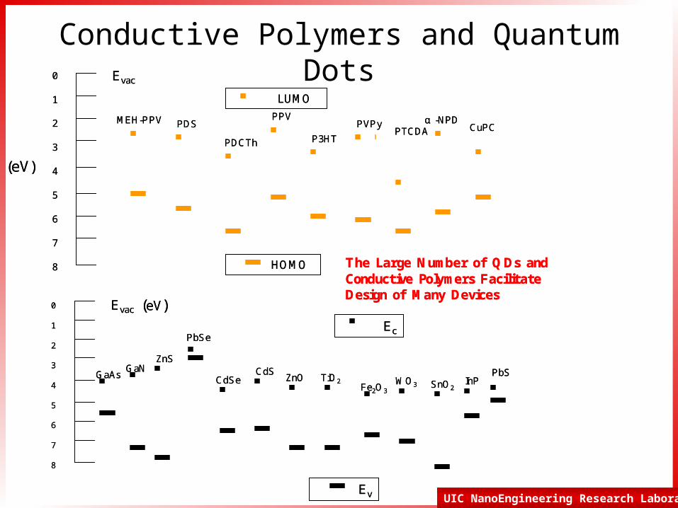
The Large Number of QDs and Conductive Polymers FacilitateDesign of Many Devices
PbS
0
1
2
3
4
5
6
7
8
Evac
PDCTh
PPVPDS PVPy
P3HT
MEH-PPV
HOMO
LUMO
(eV)
PTCDAα -NPD
CuPC
0
1
2
3
4
5
6
7
8
Evac
CdSeGaN
SnO2Fe2O3
TiO2ZnOCdS
ZnS
PbSe
GaAsWO3
Ec
Ev
(eV)
InP
The Large Number of QDs and Conductive Polymers FacilitateDesign of Many Devices
PbS
Conductive Polymers and Quantum Dots

UIC NanoEngineering Research Laboratory
Thermal transport in graphite and carbon nanotubes and the effects of point defect
scattering and boundary scattering mechanisms
Contacts
CNT
Contacts
CNT

UIC NanoEngineering Research Laboratory
( )42.36 10 m/s´
( )41.59 10 m/s´
vLA
vTA
2 2 2
2 1 1
LA TAv v v= +
41.86 10 m/sv = ´c-axis

UIC NanoEngineering Research Laboratory
2D intrinsic thermal conductivity of graphite
Two-dimensional intrinsic thermal conductivity of graphite as a function of temperature.
( )2 3 2
4
d
kfC f
a f=
( )3
2 2,4
di
Mv fl f T
kTfpg=

UIC NanoEngineering Research Laboratory
Effective average point defect concentration
…
Tub
e Dire
ction
…
Tub
e Dire
ction
Row 1st
2nd
nth
…
Tub
e Dire
ction
…
Tub
e Dire
ction
Row 1st
2nd
nth
N: number of circumferential atomsn: number of rowsln: length of CNTd: distance between 2 nearest atoms
Contacts
CNT
Contacts
CNT
For enlightening discussion on end effects see G. Mpourmpakis, G. Froudakis, A. N. Andriotis, M. Menon,
Carbon-nanotube Tips with Edge Made of a Transition Metal, APL, 87, 193105 (2005).

UIC NanoEngineering Research Laboratory
Effective average point defect concentration
…
Tub
e Direction
…
Tub
e Direction
Row 1st
2nd
nth
…
Tub
e Direction
…
Tub
e Direction
Row 1st
2nd
nth
N: number of circumferential atomsn: number of rowsln: length of CNTd: distance between 2 nearest atoms
Contacts
CNT
Contacts
CNT

UIC NanoEngineering Research Laboratory
End effects of point defects
End effects of point defects on CNT thermal conductivity:
solid line is at 300 K, dotted line is at 500 K dashed line is at 800 K

UIC NanoEngineering Research Laboratory
Compare point defect scattering and boundary scattering
Thermal conductivity as a function of CNT tube length at 300 K.
Thermal conductivity as a function of temperature for a single-wall CNT of about 21.2 nm in length:
- solid line is for boundary scattering - dotted line is for point-defect
scattering.

UIC NanoEngineering Research Laboratory
Thermoelectric figure of merit
Thermoelectric figure of merit as a function of temperature for a single-wall CNT of about 4.1 nm in length.
S is the Seebeck coefficient, σ is the electric conductivity, T is the absolute temperature and λ is the thermal conductivity
High ZT values achieved in other systems include AgPbmSbTe2+m reported to exhibit a ZT of ~2.2 at 800 K. ZT values of 2.0 at 300 K have been obtained for PbSnSeTe alloy materials and ~0.8 for the material CsBi4Te6 produced at 225 K.
ZT = S2σT/λ