
Programmable nanoengineering templates for …eezfan/Papers/paper66.pdfProgrammable nanoengineering...
9
NANO EXPRESS Open Access Programmable nanoengineering templates for fabrication of three-dimensional nanophotonic structures Qingfeng Lin, Siu-Fung Leung, Kwong-Hoi Tsui, Bo Hua and Zhiyong Fan * Abstract Porous anodic alumina membranes (AAMs) have attracted great amount of attention due to their potential application as templates for nanoengineering. Template-guided fabrication and assembly of nanomaterials based on AAMs are cost-effective and scalable methods to program and engineer the shape and morphology of nanostructures and nanomaterials. In this work, perfectly ordered AAMs with the record large pitch up to 3 μm have been fabricated by properly controlling the anodization conditions and utilization of nanoimprint technique. Due to the capability of programmable structural design and fabrication, a variety of nanostructures, including nanopillar arrays, nanotower arrays, and nanocone arrays, have been successfully fabricated using nanoengineered AAM templates. Particularly, amorphous Si nanocones have been fabricated as three-dimensional nanophotonic structures with the characterization of their intriguing optical anti-reflection property. These results directly indicate the potential application of the reported approach for photonics and optoelectronics. Keywords: Large-pitch anodic alumina membranes, Programmable nanoengineering templates, Nanocones, Three-dimensional nanophotonic structures Background The capability to program and engineer the shape and morphology of nanostructures and nanomaterials enables tailoring their electronic [1-3], optical [4-6], sensing [7,8], thermal [9,10], and mechanical [11-14] properties for a variety of applications including electronics, photovoltaics, sensors, thermoelectrics, nanomechanical devices, etc. Specifically, a variety of three-dimensional (3-D) nanopho- tonic structures, such as nanowires [15,16], nanopillars [17,18], nanowells [19], and so forth, have been extensively studied for efficient light harvesting scheme to enhance the performance of solar cells. Properly engineered 3-D nanostructures have demonstrated highly promising capability of harvesting sunlight over a broad range of wavelengths and incident angles due to their broadband anti-reflection and efficient light trapping properties. On the other hand, cost-effective approaches toward the precise control of the shape and morphology of nano- structures are crucial for any aforementioned practical ap- plications. In general, nanofabrication methods used to produce nanostructures are commonly defined as ‘top- down’ and ‘bottom-up’ methods [20]. The top-down approaches, which use various kinds of lithographic tech- niques to pattern nanoscale structures typically in two dimensions, allow to fabricate different and complex structures with high precision. However, their major dis- advantage rests in high cost and limited scalability. Con- versely, the bottom-up approaches, which utilize energetic favorable self-assembly and/or self-organizing mechanisms to form nanostructures, are cost-effective but usually lack of controllability over as-obtained macro- and nanostruc- tures. In this regard, a cost-effective and scalable method combining the advantages of both top-down and bottom- up approaches will be highly appealing. Template-guided fabrication and assembly of nanomaterials, particularly based on porous anodic alumina membranes (AAMs), have attracted great amount of attention due to the fact that AAMs are formed by self-organizing mechanism and they enable direct assembly of nanomaterials with con- trolled density [21-25]. Meanwhile, recent achievements * Correspondence: [email protected] Department of Electronic and Computer Engineering, Hong Kong University of Science and Technology, Clear Water Bay, Kowloon, Hong Kong SAR, China © 2013 Lin et al.; licensee Springer. This is an Open Access article distributed under the terms of the Creative Commons Attribution License (http://creativecommons.org/licenses/by/2.0), which permits unrestricted use, distribution, and reproduction in any medium, provided the original work is properly cited. Lin et al. Nanoscale Research Letters 2013, 8:268 http://www.nanoscalereslett.com/content/8/1/268
Transcript of Programmable nanoengineering templates for …eezfan/Papers/paper66.pdfProgrammable nanoengineering...
Lin et al. Nanoscale Research Letters 2013, 8:268http://www.nanoscalereslett.com/content/8/1/268
NANO EXPRESS Open Access
Programmable nanoengineering templates forfabrication of three-dimensional nanophotonicstructuresQingfeng Lin, Siu-Fung Leung, Kwong-Hoi Tsui, Bo Hua and Zhiyong Fan*
Abstract
Porous anodic alumina membranes (AAMs) have attracted great amount of attention due to their potentialapplication as templates for nanoengineering. Template-guided fabrication and assembly of nanomaterials basedon AAMs are cost-effective and scalable methods to program and engineer the shape and morphology ofnanostructures and nanomaterials. In this work, perfectly ordered AAMs with the record large pitch up to 3 μmhave been fabricated by properly controlling the anodization conditions and utilization of nanoimprint technique.Due to the capability of programmable structural design and fabrication, a variety of nanostructures, includingnanopillar arrays, nanotower arrays, and nanocone arrays, have been successfully fabricated using nanoengineeredAAM templates. Particularly, amorphous Si nanocones have been fabricated as three-dimensional nanophotonicstructures with the characterization of their intriguing optical anti-reflection property. These results directly indicatethe potential application of the reported approach for photonics and optoelectronics.
Keywords: Large-pitch anodic alumina membranes, Programmable nanoengineering templates, Nanocones,Three-dimensional nanophotonic structures
BackgroundThe capability to program and engineer the shape andmorphology of nanostructures and nanomaterials enablestailoring their electronic [1-3], optical [4-6], sensing [7,8],thermal [9,10], and mechanical [11-14] properties for avariety of applications including electronics, photovoltaics,sensors, thermoelectrics, nanomechanical devices, etc.Specifically, a variety of three-dimensional (3-D) nanopho-tonic structures, such as nanowires [15,16], nanopillars[17,18], nanowells [19], and so forth, have been extensivelystudied for efficient light harvesting scheme to enhancethe performance of solar cells. Properly engineered 3-Dnanostructures have demonstrated highly promisingcapability of harvesting sunlight over a broad range ofwavelengths and incident angles due to their broadbandanti-reflection and efficient light trapping properties. Onthe other hand, cost-effective approaches toward theprecise control of the shape and morphology of nano-
* Correspondence: [email protected] of Electronic and Computer Engineering, Hong Kong Universityof Science and Technology, Clear Water Bay, Kowloon, Hong Kong SAR,China
© 2013 Lin et al.; licensee Springer. This is an OAttribution License (http://creativecommons.orin any medium, provided the original work is p
structures are crucial for any aforementioned practical ap-plications. In general, nanofabrication methods used toproduce nanostructures are commonly defined as ‘top-down’ and ‘bottom-up’ methods [20]. The top-downapproaches, which use various kinds of lithographic tech-niques to pattern nanoscale structures typically in twodimensions, allow to fabricate different and complexstructures with high precision. However, their major dis-advantage rests in high cost and limited scalability. Con-versely, the bottom-up approaches, which utilize energeticfavorable self-assembly and/or self-organizing mechanismsto form nanostructures, are cost-effective but usually lackof controllability over as-obtained macro- and nanostruc-tures. In this regard, a cost-effective and scalable methodcombining the advantages of both top-down and bottom-up approaches will be highly appealing. Template-guidedfabrication and assembly of nanomaterials, particularlybased on porous anodic alumina membranes (AAMs),have attracted great amount of attention due to the factthat AAMs are formed by self-organizing mechanism andthey enable direct assembly of nanomaterials with con-trolled density [21-25]. Meanwhile, recent achievements
pen Access article distributed under the terms of the Creative Commonsg/licenses/by/2.0), which permits unrestricted use, distribution, and reproductionroperly cited.

Lin et al. Nanoscale Research Letters 2013, 8:268 Page 2 of 9http://www.nanoscalereslett.com/content/8/1/268
on controlling template regularity and internal structureclearly demonstrate their potency for the precise integra-tion of nanomaterials with high degree of freedom[17,26-28]. In this work, we present the fabrication ofAAMs with perfect regularity and unprecedented largepitch up to 3 μm by applying high-voltage anodization inconjunction with nanoimprint process. More importantly,due to the capability of programmable structural designand fabrication, a variety of nanostructures, includingnanopillar arrays, nanotower arrays, and nanocone arrays,have been successfully fabricated using nanoengineeredAAM templates. Particularly, the nanocone arrays havebeen demonstrated as excellent 3-D nanophotonic struc-tures for efficient light harvesting due to the graduallychanged effective refractive index.
Methods
MaterialsAluminum foil (0.25 mm thick, 99.99% purity) wasobtained from Alfa Aesar (Ward Hill, MA, USA), poly-imide solution (PI 2525) was purchased from HDMicroSystems (Parlin, NJ, USA), polycarbonate film(0.2 mm thick) was obtained from Suzhou Zhuonier Op-tical Materials Co., Ltd. (Suzhou, China), epoxy glue(Norland Optical Adhesive 81) was purchased from
Figure 1 Schematic fabrication process and top-view scanning electroprocess of hexagonally ordered porous AAM. (b) Top-view SEM image of 1anodization layer. (c) Top-view SEM image of 1.5-μm-pitch AAM after the sopening in the inset.
Norland Products Inc. (Cranbury, NJ, USA), siliconeelastomer and the curing agent were purchased fromDow Corning (Midland, MI, USA). All other chemicalsare products of Sigma-Aldrich (St. Louis, MO, USA).
AAM fabricationAluminum (Al) foil was cut into 1-cm by 2-cm piecesand cleaned in acetone and isopropyl alcohol. The sheetswere electrochemically polished in a 1:3 (v/v) mixture ofperchloric acid and ethanol for 2 min at 10°C. As shownin Figure 1a, the polished Al sheets were imprintedusing silicon mold (hexagonally ordered pillar array withheight of 200 nm, diameter of 200 to 500 nm, andpitches ranging from 1 to 3 μm) with a pressure of ap-proximately 2 × 10⁴ N cm−2 to initiate the perfectly or-dered AAM growth. The substrates were anodized withconditions listed in Table 1. The first anodization layerwas then etched away in a mixture of phosphoric acid(6 wt.%) and chromic acid (1.8 wt.%) at 63°C for 40 min.After etching, the second anodization was carried outunder the same conditions to obtain approximately2-μm-thick AAM. Afterward, desired pore diameters ofAAMs were obtained by wet etching with 5% phosphoricacid at 53°C. In order to achieve tri-diameter AAM, asubstrate was secondly anodized for time tA1 using thesame anodization conditions and etched in 5% phosphoric
n microscopy (SEM) images of AAM. (a) Schematic fabrication.5-μm-pitch Al concave structure after the removal of the firstecond anodization, with the cross-sectional view showing cone-shape
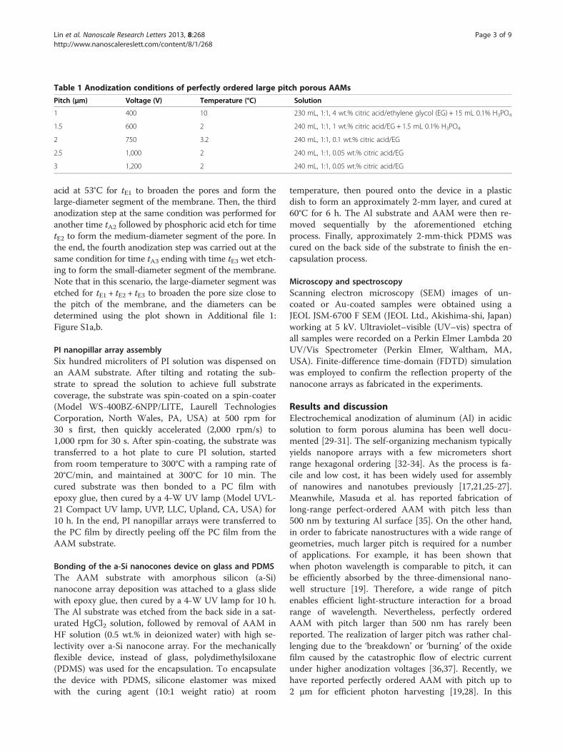
Table 1 Anodization conditions of perfectly ordered large pitch porous AAMs
Pitch (μm) Voltage (V) Temperature (°C) Solution
1 400 10 230 mL, 1:1, 4 wt.% citric acid/ethylene glycol (EG) + 15 mL 0.1% H3PO4
1.5 600 2 240 mL, 1:1, 1 wt.% citric acid/EG + 1.5 mL 0.1% H3PO4
2 750 3.2 240 mL, 1:1, 0.1 wt.% citric acid/EG
2.5 1,000 2 240 mL, 1:1, 0.05 wt.% citric acid/EG
3 1,200 2 240 mL, 1:1, 0.05 wt.% citric acid/EG
Lin et al. Nanoscale Research Letters 2013, 8:268 Page 3 of 9http://www.nanoscalereslett.com/content/8/1/268
acid at 53°C for tE1 to broaden the pores and form thelarge-diameter segment of the membrane. Then, the thirdanodization step at the same condition was performed foranother time tA2 followed by phosphoric acid etch for timetE2 to form the medium-diameter segment of the pore. Inthe end, the fourth anodization step was carried out at thesame condition for time tA3 ending with time tE3 wet etch-ing to form the small-diameter segment of the membrane.Note that in this scenario, the large-diameter segment wasetched for tE1 + tE2 + tE3 to broaden the pore size close tothe pitch of the membrane, and the diameters can bedetermined using the plot shown in Additional file 1:Figure S1a,b.
PI nanopillar array assemblySix hundred microliters of PI solution was dispensed onan AAM substrate. After tilting and rotating the sub-strate to spread the solution to achieve full substratecoverage, the substrate was spin-coated on a spin-coater(Model WS-400BZ-6NPP/LITE, Laurell TechnologiesCorporation, North Wales, PA, USA) at 500 rpm for30 s first, then quickly accelerated (2,000 rpm/s) to1,000 rpm for 30 s. After spin-coating, the substrate wastransferred to a hot plate to cure PI solution, startedfrom room temperature to 300°C with a ramping rate of20°C/min, and maintained at 300°C for 10 min. Thecured substrate was then bonded to a PC film withepoxy glue, then cured by a 4-W UV lamp (Model UVL-21 Compact UV lamp, UVP, LLC, Upland, CA, USA) for10 h. In the end, PI nanopillar arrays were transferred tothe PC film by directly peeling off the PC film from theAAM substrate.
Bonding of the a-Si nanocones device on glass and PDMSThe AAM substrate with amorphous silicon (a-Si)nanocone array deposition was attached to a glass slidewith epoxy glue, then cured by a 4-W UV lamp for 10 h.The Al substrate was etched from the back side in a sat-urated HgCl2 solution, followed by removal of AAM inHF solution (0.5 wt.% in deionized water) with high se-lectivity over a-Si nanocone array. For the mechanicallyflexible device, instead of glass, polydimethylsiloxane(PDMS) was used for the encapsulation. To encapsulatethe device with PDMS, silicone elastomer was mixedwith the curing agent (10:1 weight ratio) at room
temperature, then poured onto the device in a plasticdish to form an approximately 2-mm layer, and cured at60°C for 6 h. The Al substrate and AAM were then re-moved sequentially by the aforementioned etchingprocess. Finally, approximately 2-mm-thick PDMS wascured on the back side of the substrate to finish the en-capsulation process.
Microscopy and spectroscopyScanning electron microscopy (SEM) images of un-coated or Au-coated samples were obtained using aJEOL JSM-6700 F SEM (JEOL Ltd., Akishima-shi, Japan)working at 5 kV. Ultraviolet–visible (UV–vis) spectra ofall samples were recorded on a Perkin Elmer Lambda 20UV/Vis Spectrometer (Perkin Elmer, Waltham, MA,USA). Finite-difference time-domain (FDTD) simulationwas employed to confirm the reflection property of thenanocone arrays as fabricated in the experiments.
Results and discussionElectrochemical anodization of aluminum (Al) in acidicsolution to form porous alumina has been well docu-mented [29-31]. The self-organizing mechanism typicallyyields nanopore arrays with a few micrometers shortrange hexagonal ordering [32-34]. As the process is fa-cile and low cost, it has been widely used for assemblyof nanowires and nanotubes previously [17,21,25-27].Meanwhile, Masuda et al. has reported fabrication oflong-range perfect-ordered AAM with pitch less than500 nm by texturing Al surface [35]. On the other hand,in order to fabricate nanostructures with a wide range ofgeometries, much larger pitch is required for a numberof applications. For example, it has been shown thatwhen photon wavelength is comparable to pitch, it canbe efficiently absorbed by the three-dimensional nano-well structure [19]. Therefore, a wide range of pitchenables efficient light-structure interaction for a broadrange of wavelength. Nevertheless, perfectly orderedAAM with pitch larger than 500 nm has rarely beenreported. The realization of larger pitch was rather chal-lenging due to the ‘breakdown’ or ‘burning’ of the oxidefilm caused by the catastrophic flow of electric currentunder higher anodization voltages [36,37]. Recently, wehave reported perfectly ordered AAM with pitch up to2 μm for efficient photon harvesting [19,28]. In this
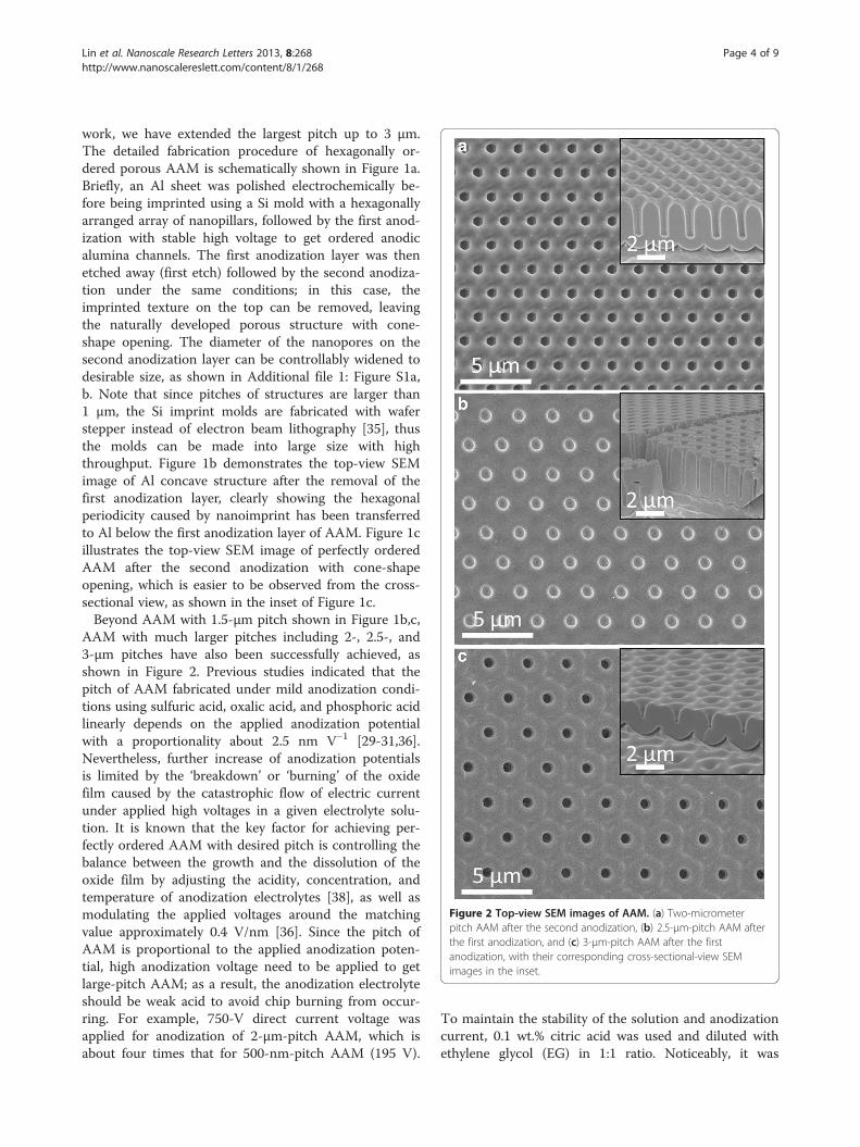
Figure 2 Top-view SEM images of AAM. (a) Two-micrometerpitch AAM after the second anodization, (b) 2.5-μm-pitch AAM afterthe first anodization, and (c) 3-μm-pitch AAM after the firstanodization, with their corresponding cross-sectional-view SEMimages in the inset.
Lin et al. Nanoscale Research Letters 2013, 8:268 Page 4 of 9http://www.nanoscalereslett.com/content/8/1/268
work, we have extended the largest pitch up to 3 μm.The detailed fabrication procedure of hexagonally or-dered porous AAM is schematically shown in Figure 1a.Briefly, an Al sheet was polished electrochemically be-fore being imprinted using a Si mold with a hexagonallyarranged array of nanopillars, followed by the first anod-ization with stable high voltage to get ordered anodicalumina channels. The first anodization layer was thenetched away (first etch) followed by the second anodiza-tion under the same conditions; in this case, theimprinted texture on the top can be removed, leavingthe naturally developed porous structure with cone-shape opening. The diameter of the nanopores on thesecond anodization layer can be controllably widened todesirable size, as shown in Additional file 1: Figure S1a,b. Note that since pitches of structures are larger than1 μm, the Si imprint molds are fabricated with waferstepper instead of electron beam lithography [35], thusthe molds can be made into large size with highthroughput. Figure 1b demonstrates the top-view SEMimage of Al concave structure after the removal of thefirst anodization layer, clearly showing the hexagonalperiodicity caused by nanoimprint has been transferredto Al below the first anodization layer of AAM. Figure 1cillustrates the top-view SEM image of perfectly orderedAAM after the second anodization with cone-shapeopening, which is easier to be observed from the cross-sectional view, as shown in the inset of Figure 1c.Beyond AAM with 1.5-μm pitch shown in Figure 1b,c,
AAM with much larger pitches including 2-, 2.5-, and3-μm pitches have also been successfully achieved, asshown in Figure 2. Previous studies indicated that thepitch of AAM fabricated under mild anodization condi-tions using sulfuric acid, oxalic acid, and phosphoric acidlinearly depends on the applied anodization potentialwith a proportionality about 2.5 nm V−1 [29-31,36].Nevertheless, further increase of anodization potentialsis limited by the ‘breakdown’ or ‘burning’ of the oxidefilm caused by the catastrophic flow of electric currentunder applied high voltages in a given electrolyte solu-tion. It is known that the key factor for achieving per-fectly ordered AAM with desired pitch is controlling thebalance between the growth and the dissolution of theoxide film by adjusting the acidity, concentration, andtemperature of anodization electrolytes [38], as well asmodulating the applied voltages around the matchingvalue approximately 0.4 V/nm [36]. Since the pitch ofAAM is proportional to the applied anodization poten-tial, high anodization voltage need to be applied to getlarge-pitch AAM; as a result, the anodization electrolyteshould be weak acid to avoid chip burning from occur-ring. For example, 750-V direct current voltage wasapplied for anodization of 2-μm-pitch AAM, which isabout four times that for 500-nm-pitch AAM (195 V).
To maintain the stability of the solution and anodizationcurrent, 0.1 wt.% citric acid was used and diluted withethylene glycol (EG) in 1:1 ratio. Noticeably, it was

Lin et al. Nanoscale Research Letters 2013, 8:268 Page 5 of 9http://www.nanoscalereslett.com/content/8/1/268
found that mixing EG with citric acid can further im-prove the stability of the electrolyte, thus avoid the burn-ing from occurring for anodization with such highvoltage [39]. Figure 2a illustrates the top-view SEMimage of perfectly ordered 2-μm-pitch AAM after thesecond anodization, with corresponding cross-sectional-view SEM image shown in the inset. The thickness ofAAM can be controlled by modifying the anodizationtime, and the pore size can be tuned by controlling theetching time.According to the rationale discussed above, 2.5- and
3-μm-pitch AAMs were also fabricated after hundredsof trials with various anodization conditions. The bestanodization conditions of these perfectly ordered large-pitch porous AAMs were summarized in Table 1. Notethat as the acids are highly diluted, anodization processoccurs in a quite slow rate; therefore, AAM growth rateis very slow as well, as shown in Additional file 1: FigureS1d. Figure 2b,c show SEM images of ordered 2.5- and3-μm-pitch AAM after the first anodization, instead ofafter the second anodization. The matching anodizationpotential for 3-μm-pitch AAM is 1,200 V, which gene-rates massive heat so that the present cooling systemwas not powerful enough to maintain the temperaturestability leading to the burning of oxide films during theanodization process gradually. Therefore, the maximumdepth of the channels in 3-μm-pitch AAM after the firstanodization we achieved was about 1 μm (inset inFigure 2c). This depth is not sufficient to form deep Alconcave texture to guide the self-assembly of porousalumina during the second anodization. Whereas themaximum pitch of ordered porous AAM achieved inthis work is up to 3 μm, it is believed that the pitch canbe further increased in the future by modifying the an-odization conditions more carefully assisted with a moreeffective cooling system.As previously mentioned, the fabrication of ordered
porous AAMs with hexagonally packed pore arrays hasattracted much interest due to their applications as tem-plates for nanoengineering. In fact, we have successfullyfabricated nanopillar and nanotower arrays with thelarge-pitch AAMs, using flexible polymer materials, i.e.,polycarbonate (PC) and PI. In order to template PCnanopillars, a PC film was pressed on an AAM on a hotplate with a temperature of 250°C for 15 min to melt PCand fill the AAM channels (Additional file 1: FigureS2a). After cooling down, PC nanopillar arrays wereobtained by directly peeling off the PC film from theAAM. Figure 3a shows the SEM image of a 2-μm-pitchAAM with 700-nm diameter for templating PC nano-pillars, and Figure 3b illustrates the 60°-tilted-angle-viewSEM image of the resulting PC nanopillar arrays with700-nm pillar diameter. In addition, as the AAM porediameter can be widened, Figure 3c shows the SEM
image of a PC nanopillar array being templated from a2-μm-pitch AAM with pore diameter of 1.5 μm. Notethat the nanopillars shown here have beads on top ofthem. These beads were formed during peeling process,as shown in Additional file 1: Figure S3.As the internal structure and shape of AAM nano-
channels can be programmed and engineered [17,36], itopens up more degree of freedom on AAM geometry con-trol. In this work, AAMs with three segments with differentchannel diameters are fabricated by controlling etching andanodization time. Additional file 1: Figure S4 illustrates theschematic process. In brief, a substrate has undergone thesecond anodization for time tA1 and etched for tE1 tobroaden the pores and form the large-diameter segment ofthe membrane. Then, the third anodization step wasperformed for another time tA2 followed by chemical etchfor time tE2 to form the medium-diameter segment. In theend, the fourth anodization step was carried out for timetA3 ending with time tE3 wet etching to form the small-diameter segment. Note that in this scenario the first seg-ment (Figure 3d) was etched for time tE1 + tE2 + tE3, and thethird segment was etched only for tE3 to broaden the poresize. In a generalized case, if there are n segments in total,the total etching time for the mth segment will beTEm ¼ ∑n
i¼mtEi . Therefore, the diameter of the mth seg-ment can be determined by the etching calibration curveand the fitted function (Additional file 1: Figure S1a,b)Dm ¼ F TEmð Þ ¼ F ∑n
i¼mtEi� �
. In addition, the total depth ofthe AAM substrate is HTotal ¼ ∑n
i¼1H i with the mthsegment's depth of Hm =G(tAm) which can be determinedby the plots shown in Additional file 1: Figure S1c,d.Figure 3d demonstrates the cross section of a 1-μm-pitchtri-diameter AAM fabricated by a four-step anodizationprocess. Such a structure has been used to template PCnanotowers, as shown in Figure 3e,f, by the aforementionedthermal press process (Additional file 1: Figure S2b). Notethat as the length of each diameter segment is controllable,a smooth internal slope on the side wall can be achieved byproperly shortening each segment. Therefore, a nanoconestructure can be obtained, as shown in Figure 3f.It is worth noting that the above nanostructure
templating process can be extended to other materials.In practice, we have also fabricated PI nanopillar arrays(Additional file 1: Figure S3) with spin-coating method.Besides using thermal press method to template nano-structures, material deposition method was also used tofabricate well designed nanostructures with AAM. Par-ticularly, a-Si nanocone arrays have been fabricated withplasma-enhanced chemical vapor deposition (PECVD),as shown in Figure 4a with the inset showing the AAMtemplate. The nanocones are formed by a-Si thin-filmdeposition. Additional file 1: Figure S5 shows the crosssection of the a-Si nanocones embedded in the AAM. Inorder to characterize the nanocones, they are transferred
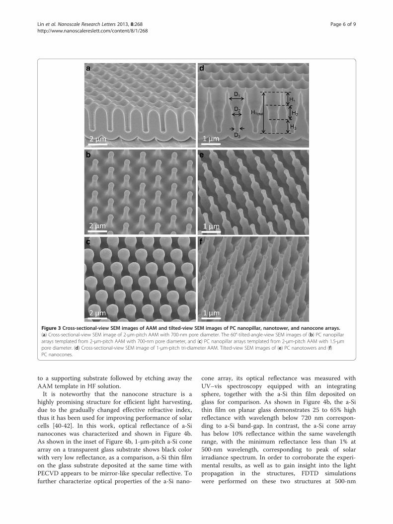
Figure 3 Cross-sectional-view SEM images of AAM and tilted-view SEM images of PC nanopillar, nanotower, and nanocone arrays.(a) Cross-sectional-view SEM image of 2-μm-pitch AAM with 700-nm pore diameter. The 60°-tilted-angle-view SEM images of (b) PC nanopillararrays templated from 2-μm-pitch AAM with 700-nm pore diameter, and (c) PC nanopillar arrays templated from 2-μm-pitch AAM with 1.5-μmpore diameter. (d) Cross-sectional-view SEM image of 1-μm-pitch tri-diameter AAM. Tilted-view SEM images of (e) PC nanotowers and (f)PC nanocones.
Lin et al. Nanoscale Research Letters 2013, 8:268 Page 6 of 9http://www.nanoscalereslett.com/content/8/1/268
to a supporting substrate followed by etching away theAAM template in HF solution.It is noteworthy that the nanocone structure is a
highly promising structure for efficient light harvesting,due to the gradually changed effective refractive index,thus it has been used for improving performance of solarcells [40-42]. In this work, optical reflectance of a-Sinanocones was characterized and shown in Figure 4b.As shown in the inset of Figure 4b, 1-μm-pitch a-Si conearray on a transparent glass substrate shows black colorwith very low reflectance, as a comparison, a-Si thin filmon the glass substrate deposited at the same time withPECVD appears to be mirror-like specular reflective. Tofurther characterize optical properties of the a-Si nano-
cone array, its optical reflectance was measured withUV–vis spectroscopy equipped with an integratingsphere, together with the a-Si thin film deposited onglass for comparison. As shown in Figure 4b, the a-Sithin film on planar glass demonstrates 25 to 65% highreflectance with wavelength below 720 nm correspon-ding to a-Si band-gap. In contrast, the a-Si cone arrayhas below 10% reflectance within the same wavelengthrange, with the minimum reflectance less than 1% at500-nm wavelength, corresponding to peak of solarirradiance spectrum. In order to corroborate the experi-mental results, as well as to gain insight into the lightpropagation in the structures, FDTD simulationswere performed on these two structures at 500-nm
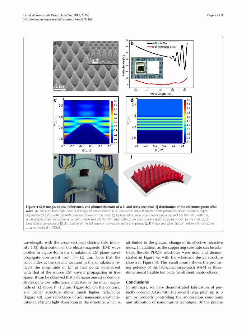
Figure 4 SEM image, optical reflectance, and photo/schematic of a-Si and cross-sectional |E| distribution of the electromagnetic (EM)wave. (a) The 60°-tilted-angle-view SEM image of amorphous Si (a-Si) nanocone arrays fabricated with plasma-enhanced chemical vapordeposition (PECVD), with the AAM template shown in the inset. (b) Optical reflectance of a-Si nanocone array and a-Si thin film, with thephotographs of a-Si nanocone array (left photo) and a-Si thin film (right photo) on a transparent glass substrate shown in the inset. (c, d)Simulated cross-sectional |E| distribution of the EM wave on nanocone arrays and planar. (e, f) Photo and schematic of flexible a-Si nanoconearray embedded in PDMS.
Lin et al. Nanoscale Research Letters 2013, 8:268 Page 7 of 9http://www.nanoscalereslett.com/content/8/1/268
wavelength, with the cross-sectional electric field inten-sity (|E|) distribution of the electromagnetic (EM) waveplotted in Figure 4c. In the simulations, EM plane wavespropagate downward from Y = 1.5 μm. Note that thecolor index at the specific location in the simulations re-flects the magnitude of |E| at that point, normalizedwith that of the source EM wave if propagating in freespace. It can be observed that a-Si nanocone array demon-strates quite low reflectance, indicated by the small magni-tude of |E| above Y = 1.5 μm (Figure 4c). On the contrary,a-Si planar structure shows much higher reflectance(Figure 4d). Low reflectance of a-Si nanocone array indi-cates an efficient light absorption in the structure, which is
attributed to the gradual change of its effective refractiveindex. In addition, as the supporting substrate can be arbi-trary, flexible PDMS substrates were used and demon-strated in Figure 4e, with the schematic device structureshown in Figure 4f. This result clearly shows the promis-ing potency of the fabricated large-pitch AAM as three-dimensional flexible template for efficient photovoltaics.
ConclusionsIn summary, we have demonstrated fabrication of per-fectly ordered AAM with the record large pitch up to 3μm by properly controlling the anodization conditionsand utilization of nanoimprint technique. By the precise

Lin et al. Nanoscale Research Letters 2013, 8:268 Page 8 of 9http://www.nanoscalereslett.com/content/8/1/268
structure design and control, a number of uniquenanostructures, including nanopillars, nanotowers, andnanocones, have been successfully fabricated usinglarge-pitch AAMs as nanoengineering templates. Thisapproach can be extended to a variety of other complexstructures compatible with diverse materials. Particu-larly, a-Si nanocones have been fabricated as 3-Dnanophotonic structures with characterization of theirintriguing optical anti-reflection property. These resultsdirectly indicate the potential application of the reportedapproach for photonics and optoelectronics.
Additional file
Additional file 1: Supporting Information. The file contains Figure S1to Figure S5.
Competing interestsThe authors declare that they have no competing interests.
Authors’ contributionsQL prepared the AAM templates, carried out the reflectance spectrum of a-Sinanocone arrays by both experiments and simulations, and drafted themanuscript. SFL fabricated a-Si nanocone arrays based on the AAMtemplates. KHT helped on the fabrication of PC nanostructures based on theAAM templates. BH gave some suggestions on FDTD simulations. ZFprovided the idea and completed the manuscript. All authors read andapproved the final manuscript.
AcknowledgmentsThis work was partially supported by ITS/192/11 from Hong Kong InnovationTechnology Commission, HKUST Research Project Competition Grant(RPC11EG38), General Research Fund (612111) from Hong Kong ResearchGrant Council, and National Research Foundation of Korea funded by theKorean Government (NRF-2010-220-D00060, 2008–0662256). Supportinginformation is available online from Wiley InterScience or from the author.
Received: 14 May 2013 Accepted: 28 May 2013Published: 7 June 2013
References1. Hong WK, Sohn JI, Hwang DK, Kwon SS, Jo G, Song S, Kim SM, Ko HJ,
Park SJ, Welland ME: Tunable electronic transport characteristics ofsurface-architecture-controlled ZnO nanowire field effect transistors.Nano Lett 2008, 8:950–956.
2. Chang PC, Fan ZY, Wang DW, Tseng WY, Chiou WA, Hong J, Lu JG: ZnOnanowires synthesized by vapor trapping CVD method. Chem Mater2004, 16:5133–5137.
3. Kapadia R, Fan Z, Javey A: Design constraints and guidelines for CdS/CdTenanopillar based photovoltaics. Appl Phys Lett 2010, 96:103116.
4. Yeh LK, Lai KY, Lin GJ, Fu PH, Chang HC, Lin CA, He JH: Giant efficiencyenhancement of GaAs solar cells with graded antireflection layers basedon syringelike ZnO nanorod arrays. Adv Energy Mater 2011, 1:506–510.
5. Chueh YL, Fan ZY, Takei K, Ko H, Kapdia R, Rathore A, Miller N, Yu K, Wu M,Haller EE, Javey A: Black Ge based on crystalline/amorphous core/shellnanoneedle arrays. Nano Lett 2010, 10:520–523.
6. Hua B, Lin Q, Zhang Q, Fan Z: Efficient photon management withnanostructures for photovoltaics. Nanoscale 2013. doi:10.1039/C3NR01152F.
7. Park W, Jo G, Hong WK, Yoon J, Choe M, Lee S, Ji Y, Kim G, Kahng YH, Lee K:Enhancement in the photodetection of ZnO nanowires by introducingsurface-roughness-induced traps. Nanotechnology 2011, 22:205204–205209.
8. Shaalan N, Yamazaki T, Kikuta T: Influence of morphology and structuregeometry on NO2 gas-sensing characteristics of SnO2 nanostructuressynthesized via a thermal evaporation method. Sensors Actuators B: Chem2011, 153:11–16.
9. Hochbaum AI, Chen RK, Delgado RD, Liang WJ, Garnett EC, Najarian M,Majumdar A, Yang PD: Enhanced thermoelectric performance of roughsilicon nanowires. Nature 2008, 451:163–168.
10. Pichanusakorn P, Bandaru P: Nanostructured thermoelectrics. Mater Sci EngR 2010, 67:19–63.
11. Stan G, Ciobanu C, Parthangal P, Cook R: Diameter-dependent radial andtangential elastic moduli of ZnO nanowires. Nano Lett 2007, 7:3691–3697.
12. Bai X, Gao P, Wang ZL, Wang E: Dual-mode mechanical resonance ofindividual ZnO nanobelts. Appl Phys Lett 2003, 82:4806–4808.
13. Ko H, Zhang ZX, Chueh YL, Ho JC, Lee J, Fearing RS, Javey A: Wet and dryadhesion properties of self-selective nanowire connectors. Adv EnergyMater 2009, 19:3098–3102.
14. Ko H, Zhang Z, Takei K, Javey A: Hierarchical polymer micropillar arraysdecorated with ZnO nanowires. Nanotechnology 2010, 21:295305–295309.
15. Chao Y, Chen C, Lin C, He J: Light scattering by nanostructuredanti-reflection coatings. Energ Environ Sci 2011, 4:3436–3441.
16. Chang H, Lai K, Dai Y, Wang H, Lin C, He J: Nanowire arrays withcontrolled structure profiles for maximizing optical collection efficiency.Energ Environ Sci 2011, 4:2863–2869.
17. Fan ZY, Kapadia R, Leu PW, Zhang XB, Chueh YL, Takei K, Yu K, Jamshidi A,Rathore AA, Ruebusch DJ, Wu M, Javey A: Ordered arrays of dual-diameternanopillars for maximized optical absorption. Nano Lett 2010, 10:3823–3827.
18. Hua B, Wang B, Leu PW, Fan ZY: Rational geometrical design ofmulti-diameter nanopillars for efficient light harvesting. Nano Energy2013. doi:10.1016/j.nanoen.2013.03.016.
19. Leung SF, Yu M, Lin Q, Kwon K, Ching KL, Gu L, Yu K, Fan Z: Efficientphoton capturing with ordered three-dimensional nanowell arrays.Nano Lett 2012, 12:3682–3689.
20. Gates BD, Xu Q, Stewart M, Ryan D, Willson CG, Whitesides GM: Newapproaches to nanofabrication: molding, printing, and other techniques.Chem Rev 2005, 105:1171–1196.
21. Fan ZY, Dutta D, Chien CJ, Chen HY, Brown EC, Chang PC, Lu JG: Electricaland photoconductive properties of vertical ZnO nanowires in highdensity arrays. Appl Phys Lett 2006, 89:213110–213112.
22. Masuda H, Fukuda K: Ordered metal nanohole arrays made by a two-stepreplication of honeycomb structures of anodic alumina. Science 1995,268:1466–1468.
23. Yanagishita T, Sasaki M, Nishio K, Masuda H: Carbon nanotubes with atriangular cross-section, fabricated using anodic porous alumina as thetemplate. Adv Mater 2004, 16:429–432.
24. Banerjee P, Perez I, Henn-Lecordier L, Lee SB, Rubloff GW: Nanotubularmetal-insulator-metal capacitor arrays for energy storage.Nat Nanotechnol 2009, 4:292–296.
25. Steinhart M, Wendorff JH, Greiner A, Wehrspohn RB, Nielsch K, Schilling J,Choi J, Gosele U: Polymer nanotubes by wetting of ordered poroustemplates. Science 2002, 296:1997–1997.
26. Fan ZY, Razavi H, Do JW, Moriwaki A, Ergen O, Chueh YL, Leu PW, Ho JC,Takahashi T, Reichertz LA, Neale S, Yu K, Wu M, Ager JW, Javey A: Threedimensional nanopillar array photovoltaics on low cost and flexiblesubstrate. Nat Mater 2009, 8:648–653.
27. Ergen O, Ruebusch DJ, Fang H, Rathore AA, Kapadia R, Fan Z, Takei K,Jamshidi A, Wu M, Javey A: Shape-controlled synthesis of single-crystalline nanopillar arrays by template-assisted vapor–liquid-solidprocess. J Am Chem Soc 2010, 132:13972–13974.
28. Lin Q, Hua B, Leung S, Duan X, Fan Z: Efficient light absorption withintegrated nanopillar/nanowell arrays for three-dimensional thin-filmphotovoltaic applications. ACS Nano 2013, 7:2725–2732.
29. Keller F, Hunter M, Robinson D: Structural features of oxide coatings onaluminum. J Electrochem Soc 1953, 100:411–419.
30. Ebihara K, Takahashi H, Nagayama M: Structure and density of anodicoxide films formed on aluminium in oxalic acid solutions. J Met Finish SocJpn 1983, 34:548–553.
31. O'sullivan J, Wood G: The morphology and mechanism of formation of porousanodic films on aluminium. Proc R Soc London Ser A 1970, 317:511–543.
32. Masuda H, Yada K, Osaka A: Self-ordering of cell configuration of anodicporous alumina with large-size pores in phosphoric acid solution.Jpn J Appl Phys 1998, 37:L1340–L1342.
33. Jessensky O, Muller F, Gosele U: Self-organized formation of hexagonalpore arrays in anodic alumina. Appl Phys Lett 1998, 72:1173–1175.
34. Nielsch K, Choi J, Schwirn K, Wehrspohn RB, Gösele U: Self-ordering regimesof porous alumina: the 10% porosity rule. Nano Lett 2002, 2:677–680.
Lin et al. Nanoscale Research Letters 2013, 8:268 Page 9 of 9http://www.nanoscalereslett.com/content/8/1/268
35. Masuda H, Yamada H, Satoh M, Asoh H, Nakao M, Tamamura T: Highlyordered nanochannel-array architecture in anodic alumina. Appl Phys Lett1997, 71:2770–2772.
36. Lee W, Ji R, Gösele U, Nielsch K: Fast fabrication of long-range ordered porousalumina membranes by hard anodization. Nat Mater 2006, 5:741–747.
37. Ono S, Saito M, Ishiguro M, Asoh H: Controlling factor of self-ordering ofanodic porous alumina. J Electrochem Soc 2004, 151:B473–B478.
38. Chu S, Wada K, Inoue S, Isogai M, Katsuta Y, Yasumori A: Large-scalefabrication of ordered nanoporous alumina films with arbitrary poreintervals by critical-potential anodization. J Electrochem Soc 2006,153:B384–B391.
39. Yu R, Ching K, Lin Q, Leung S, Arcrossito D, Fan Z: Strong light absorptionof self-organized 3-D nanospike arrays for photovoltaic applications.ACS Nano 2011, 5:9291–9298.
40. Garnett EC, Brongersma ML, Cui Y, McGehee MD: Nanowire solar cells.Annu Rev Mater Res 2011, 41:269–295.
41. Hsu CM, Battaglia C, Pahud C, Ruan Z, Haug FJ, Fan S, Ballif C, Cui Y:High-efficiency amorphous silicon solar cell on a periodic nanoconeback reflector. Adv Energy Mater 2012, 2:628–633.
42. Jeong S, Garnett EC, Wang S, Yu Z, Fan S, Brongersma ML, McGehee MD,Cui Y: Hybrid silicon nanocone-polymer solar cells. Nano Lett 2012,12:2971–2976.
doi:10.1186/1556-276X-8-268Cite this article as: Lin et al.: Programmable nanoengineering templatesfor fabrication of three-dimensional nanophotonic structures. NanoscaleResearch Letters 2013 8:268.
Submit your manuscript to a journal and benefi t from:
7 Convenient online submission
7 Rigorous peer review
7 Immediate publication on acceptance
7 Open access: articles freely available online
7 High visibility within the fi eld
7 Retaining the copyright to your article
Submit your next manuscript at 7 springeropen.com