Webinar High potential global claims: creation and validation
Upload
truongdienCategory
view
216download
0
Application ReportSZZA034 - September 2002
1
TI IBIS File Creation, Validation, and Distribution ProcessesMoshiul Haque Standard Linear & Logic
ABSTRACT
The Input/Output Buffer Information Specification (IBIS), also known as ANSI/EIA-656, hasbecome widely accepted among electronic design automation (EDA) vendors,semiconductor vendors, and system designers as the format for digital electrical interfacedata. Because IBIS models do not reveal proprietary, internal processes, or architecturalinformation, semiconductor vendors’ support for IBIS continues to grow. IBIS models are oneof the most important tools used to support TI customers. TI’s goal is to create IBIS modelsthat are compatible with the latest IBIS specifications for every new logic part. This applicationreport describes TI’s IBIS creation, validation, and distribution process, so that customerscan be better informed about our IBIS models. This application report also discusses theaccuracy of IBIS models provided by TI.
Contents
1 Introduction 3. . . . . . . . . . . . . . . . . . . . . . . . . . . . . . . . . . . . . . . . . . . . . . . . . . . . . . . . . . . . . . . . . . . . . . . . . 1.1 What is IBIS? 3. . . . . . . . . . . . . . . . . . . . . . . . . . . . . . . . . . . . . . . . . . . . . . . . . . . . . . . . . . . . . . . . . . . . 1.2 History of IBIS 3. . . . . . . . . . . . . . . . . . . . . . . . . . . . . . . . . . . . . . . . . . . . . . . . . . . . . . . . . . . . . . . . . . . . 1.3 IBIS and SPICE 3. . . . . . . . . . . . . . . . . . . . . . . . . . . . . . . . . . . . . . . . . . . . . . . . . . . . . . . . . . . . . . . . . .
2 Brief Description of Some Common Types of IBIS Models. 3. . . . . . . . . . . . . . . . . . . . . . . . . . . . . . 2.1 Input Model 4. . . . . . . . . . . . . . . . . . . . . . . . . . . . . . . . . . . . . . . . . . . . . . . . . . . . . . . . . . . . . . . . . . . . . . 2.2 2-State Output 6. . . . . . . . . . . . . . . . . . . . . . . . . . . . . . . . . . . . . . . . . . . . . . . . . . . . . . . . . . . . . . . . . . . 2.3 3-State Model 11. . . . . . . . . . . . . . . . . . . . . . . . . . . . . . . . . . . . . . . . . . . . . . . . . . . . . . . . . . . . . . . . . . . 2.4 Input/Output Model 11. . . . . . . . . . . . . . . . . . . . . . . . . . . . . . . . . . . . . . . . . . . . . . . . . . . . . . . . . . . . . . 2.5 Open-Drain Model 12. . . . . . . . . . . . . . . . . . . . . . . . . . . . . . . . . . . . . . . . . . . . . . . . . . . . . . . . . . . . . . .
3 IBIS Creation 13. . . . . . . . . . . . . . . . . . . . . . . . . . . . . . . . . . . . . . . . . . . . . . . . . . . . . . . . . . . . . . . . . . . . . . . 3.1 SPICE Simulation Setup for IBIS Data 13. . . . . . . . . . . . . . . . . . . . . . . . . . . . . . . . . . . . . . . . . . . . . .
3.1.1 Pullup 13. . . . . . . . . . . . . . . . . . . . . . . . . . . . . . . . . . . . . . . . . . . . . . . . . . . . . . . . . . . . . . . . . . . 3.1.2 Pulldown 13. . . . . . . . . . . . . . . . . . . . . . . . . . . . . . . . . . . . . . . . . . . . . . . . . . . . . . . . . . . . . . . . . 3.1.3 Ground Clamp 14. . . . . . . . . . . . . . . . . . . . . . . . . . . . . . . . . . . . . . . . . . . . . . . . . . . . . . . . . . . . 3.1.4 Power Clamp 14. . . . . . . . . . . . . . . . . . . . . . . . . . . . . . . . . . . . . . . . . . . . . . . . . . . . . . . . . . . . . 3.1.5 Ramp, Rising, and Falling Waveform Data 14. . . . . . . . . . . . . . . . . . . . . . . . . . . . . . . . . . . 3.1.6 C_comp 16. . . . . . . . . . . . . . . . . . . . . . . . . . . . . . . . . . . . . . . . . . . . . . . . . . . . . . . . . . . . . . . . .
3.2 IBIS File Data Extraction and Formatting 16. . . . . . . . . . . . . . . . . . . . . . . . . . . . . . . . . . . . . . . . . . .
4 IBIS File Validation 17. . . . . . . . . . . . . . . . . . . . . . . . . . . . . . . . . . . . . . . . . . . . . . . . . . . . . . . . . . . . . . . . . .
5 Visual Check of IBIS Waveform 17. . . . . . . . . . . . . . . . . . . . . . . . . . . . . . . . . . . . . . . . . . . . . . . . . . . . . . 5.1 Pullup Waveforms 18. . . . . . . . . . . . . . . . . . . . . . . . . . . . . . . . . . . . . . . . . . . . . . . . . . . . . . . . . . . . . . . 5.2 Pulldown Waveforms 19. . . . . . . . . . . . . . . . . . . . . . . . . . . . . . . . . . . . . . . . . . . . . . . . . . . . . . . . . . . . . 5.3 Rising Waveforms 20. . . . . . . . . . . . . . . . . . . . . . . . . . . . . . . . . . . . . . . . . . . . . . . . . . . . . . . . . . . . . . .
Trademarks are the property of their respective owners.

SZZA034
2 TI IBIS File Creation, Validation, and Distribution Processes
5.4 Falling Waveform 21. . . . . . . . . . . . . . . . . . . . . . . . . . . . . . . . . . . . . . . . . . . . . . . . . . . . . . . . . . . . . . . . 5.5 Ground-Clamp Waveforms 22. . . . . . . . . . . . . . . . . . . . . . . . . . . . . . . . . . . . . . . . . . . . . . . . . . . . . . . . 5.6 Bus-Hold Behavior in Ground-Clamp Data 23. . . . . . . . . . . . . . . . . . . . . . . . . . . . . . . . . . . . . . . . . . 5.7 Power-Clamp Waveforms 24. . . . . . . . . . . . . . . . . . . . . . . . . . . . . . . . . . . . . . . . . . . . . . . . . . . . . . . . .
6 IBIS File Warnings and Errors 24. . . . . . . . . . . . . . . . . . . . . . . . . . . . . . . . . . . . . . . . . . . . . . . . . . . . . . .
7 IBIS File Distribution 26. . . . . . . . . . . . . . . . . . . . . . . . . . . . . . . . . . . . . . . . . . . . . . . . . . . . . . . . . . . . . . . .
8 Resources 26. . . . . . . . . . . . . . . . . . . . . . . . . . . . . . . . . . . . . . . . . . . . . . . . . . . . . . . . . . . . . . . . . . . . . . . . .
9 References 26. . . . . . . . . . . . . . . . . . . . . . . . . . . . . . . . . . . . . . . . . . . . . . . . . . . . . . . . . . . . . . . . . . . . . . . . .
Appendix-A. Using IBIS Model in HSPICE Simulation 27. . . . . . . . . . . . . . . . . . . . . . . . . . . . . . . . . . . . . .
List of Figures
Figure 1. Input Model Structure 4. . . . . . . . . . . . . . . . . . . . . . . . . . . . . . . . . . . . . . . . . . . . . . . . . . . . . . . . . . Figure 2. Test Simulation Setup to Compare the Difference in Voltage Waveforms
Due to R_fixture 7. . . . . . . . . . . . . . . . . . . . . . . . . . . . . . . . . . . . . . . . . . . . . . . . . . . . . . . . . . . . . . Figure 3. Comparison of Voltage Waveforms for IBIS Model Created
With 50-Ω and 500-Ω Loads 8. . . . . . . . . . . . . . . . . . . . . . . . . . . . . . . . . . . . . . . . . . . . . . . . . . . . Figure 4. V_fixture, R_fixture, C_fixture, and L_fixture in AC Test 8. . . . . . . . . . . . . . . . . . . . . . . . . . . . Figure 5. Two-State Output Model Structure 9. . . . . . . . . . . . . . . . . . . . . . . . . . . . . . . . . . . . . . . . . . . . . . Figure 6. Rref, Cref, and Vref During Propagation Delay Test 9. . . . . . . . . . . . . . . . . . . . . . . . . . . . . . . . Figure 7. Data-Sheet Parameter Measurement Information 10. . . . . . . . . . . . . . . . . . . . . . . . . . . . . . . . Figure 8. Parameter-Measurement Information for GTLP Devices 10. . . . . . . . . . . . . . . . . . . . . . . . . . Figure 9. Vmeas in Propagation Delay Measurement. 10. . . . . . . . . . . . . . . . . . . . . . . . . . . . . . . . . . . . . Figure 10. 3-State Output Model Structure 11. . . . . . . . . . . . . . . . . . . . . . . . . . . . . . . . . . . . . . . . . . . . . . . . Figure 11. Input/Output Buffer Model Structure 12. . . . . . . . . . . . . . . . . . . . . . . . . . . . . . . . . . . . . . . . . . . . Figure 12. SPICE Setup to Extract Pullup Data 13. . . . . . . . . . . . . . . . . . . . . . . . . . . . . . . . . . . . . . . . . . . . Figure 13. SPICE Setup to Extract Pulldown Data 14. . . . . . . . . . . . . . . . . . . . . . . . . . . . . . . . . . . . . . . . . Figure 14. SPICE Setup for V-T data (R_fixture Connected to Pullup Reference) 15. . . . . . . . . . . . . . . Figure 15. SPICE Setup for V-T Data (R_fixture Connected to Pulldown Reference) 16. . . . . . . . . . . . Figure 16. SPICE Setup to Measure C_comp 16. . . . . . . . . . . . . . . . . . . . . . . . . . . . . . . . . . . . . . . . . . . . . Figure 17. Pullup Waveforms 18. . . . . . . . . . . . . . . . . . . . . . . . . . . . . . . . . . . . . . . . . . . . . . . . . . . . . . . . . . . Figure 18. Pulldown Waveforms 19. . . . . . . . . . . . . . . . . . . . . . . . . . . . . . . . . . . . . . . . . . . . . . . . . . . . . . . . . Figure 19. Rising Waveforms 20. . . . . . . . . . . . . . . . . . . . . . . . . . . . . . . . . . . . . . . . . . . . . . . . . . . . . . . . . . . Figure 20. Falling Waveforms 21. . . . . . . . . . . . . . . . . . . . . . . . . . . . . . . . . . . . . . . . . . . . . . . . . . . . . . . . . . . Figure 21. Ground-Clamp Waveforms 22. . . . . . . . . . . . . . . . . . . . . . . . . . . . . . . . . . . . . . . . . . . . . . . . . . . . Figure 22. Bus-Hold Behavior in Ground-Clamp Data 23. . . . . . . . . . . . . . . . . . . . . . . . . . . . . . . . . . . . . . Figure 23. Power-Clamp Waveforms 24. . . . . . . . . . . . . . . . . . . . . . . . . . . . . . . . . . . . . . . . . . . . . . . . . . . . .

SZZA034
3 TI IBIS File Creation, Validation, and Distribution Processes
1 Introduction
1.1 What is IBIS?
The input/output buffer information specification (IBIS) is a behavioral-modeling specification. Itis a standard for describing the analog behavior of the buffers of a digital device using plainASCII-text formatted data. The data in an IBIS file is used to perform signal integrity (SI)simulations of printed circuit boards. The information needed to perform this simulation is buffervoltage-current (V-I) characteristics and switching (output voltage versus time) characteristics.
1.2 History of IBIS
IBIS was created in the early 1990s to promote tool-independent I/O models for system-levelsignal-integrity work. PCI bus signal-integrity simulations were ramping up at Intel, but no onehad a PCI buffer designed. In general, SPICE models were not commonly available. Toovercome this problem, Intel developed a behavioral buffer model in HSPICE that simulatesany buffer characteristics. The behavioral model was so successful that Intel decided to supplyit to customers. But, all customers did not use HSPICE, so a tool-independent model format wasneeded. Several electronic design automation (EDA) tool vendors showed interest in a commonmodeling format, and the IBIS open forum was formed. The first IBIS specification, 1.0, wasreleased in April 1993.
1.3 Input Model
SPICE models are the most widely used models. SPICE models are based on transistor-levelmodeling. For complicated electronic circuits, the total time required to complete a simulation inSPICE is long. SPICE models also should be encrypted, or there should be a nondisclosureagreement (NDA) in place to protect proprietary information. On the other hand, IBIS is abehavioral model and does not reveal any proprietary information. Because IBIS is a behavioralmodel, the total time for simulation is much less than for SPICE.
2 Brief Description of Some Common Types of IBIS Models
An IBIS file of a device contains the electrical characteristics of all the unique pins of that device.Electrical characteristics of a specific pin are called an IBIS model of that pin. An IBIS file alsocontains the package resistance, inductance, and capacitance (R, L, and C) data for each pin.
The following are the most common types of pins in a digital-logic device:
• Input
• 2-state output
• 3-state output
• Input/output (I/O)
• Open drain
Similarly, the model in an IBIS file can be input, 3-state, I/O, etc.

SZZA034
4 TI IBIS File Creation, Validation, and Distribution Processes
2.1 Input Model
The input pin structure of a digital device can be thought of as a combination of the followingcircuits and elements.
• A circuit that is activated if the input voltage is over VCC or logic high (power clamp)
• A circuit that is activated if the input voltage is below ground or logic low (ground clamp)
• A circuit that is activated if the input is within VCC and ground (active circuit)
• Resistance, inductance, and capacitance of the package (R, L, and C)
• Die capacitance of the input pin
The data for these circuits and elements are described under several keywords in the IBIS file.IBIS keywords are shown in square brackets.
The behavior of the first circuit is listed under the [POWER Clamp] keyword, and the behaviorsof the latter two circuits are listed under the [GND Clamp] keyword. R, L, and C are listed underthe [Pin] keyword. Most often, a CMOS digital device has the input structure shown in Figure 1.In this input structure, VDD is the power-clamp reference because the upper clamp diode isconnected to the dc voltage source VDD†, and –VSS† is the ground-clamp reference because thelower clamp diode is connected to the dc voltage source –VSS. The details of power-clamp andthe ground-clamp references are discussed later in this application report. Even though thepackage R, L, and C data are included for the input pin, the ground-clamp and power-clampdata for the IBIS model are extracted without package data; i.e., package R, L, and C do nothave any effect on this data.
L_pkg
R_pkg
C_pkg
To Internal Circuit
C_comp
Input
–VSS –VSS –VSS –VSS
VDDVDD
Figure 1. Input Model Structure
The upper clamp diode is forward biased when the input is approximately 0.7 V over VDD. Thelower clamp diode is forward biased when the input is approximately 0.7 V less than –VSS.
† VDD is equivalent to VCC or power supply and –VSS is equivalent to GND in TI digital logic devices.

SZZA034
5 TI IBIS File Creation, Validation, and Distribution Processes
The input-type model has the following data. Subparameters are enclosed in parentheses.
• Maximum lower threshold voltage (Vinl): VIL in the data sheet.
• Minimum upper threshold voltage (Vinh): VIH in the data sheet.
• Power-clamp reference [Power Clamp Reference]: In most digital circuits, the power-clampreference voltage is VCC because the power-clamp diode is connected to VCC. However, insome cases it may be different than the VCC or power supply. For example, with 5-V safe3.3-V buffers, the power-clamp reference is 5 V.
• Ground-clamp reference [GND Clamp Reference]: In most digital circuits, the ground-clampreference voltage is 0. However, in some cases it may be different than the ground. Forexample, in RS-232 devices it is –12 V.
• Recommended power supply [Voltage Range].
• Recommended temperature [Temperature Range]: The junction temperature of transistors.
• C_comp data (C_comp): This is the total die capacitance as seen at the die pad. C_compdoes not include package capacitance. It includes parasitic capacitance of transistors andcircuit elements, metal capacitance-connecting transistors with the die pad, and die-padcapacitance.
• Power-clamp data [POWER Clamp]: Voltage-current characteristics of the power-clampcircuit. This data is referenced to the power-clamp reference voltage, i.e., in the IBIS file thepower clamp voltage is Vtable = [Power Clamp Reference] – Vin, where Vin is the voltagereferenced to ground. For example, if power-clamp reference is VCC, then the voltage data inIBIS file is Vtable = VCC – Vin. This is the voltage across the diode, not the input voltage.
• Ground-clamp data [GND Clamp]: Voltage-current characteristics of the ground-clampcircuit. This data is referenced to ground-clamp reference voltage, i.e., in an IBIS file theground-clamp voltage is Vtable = Vin – [GND Clamp Reference], where Vin is the voltagereferenced to ground. For example, if the ground-clamp reference is ground, the voltagedata in the IBIS file is Vtable = Vin.
If the power-clamp reference voltage is not mentioned, then, by default, it is equal to therecommended power-supply voltage. Similarly, if the ground-clamp reference voltage is notmentioned, then, by default, it is equal to ground or 0.
The range of data is based on the worst-case scenario of a transmission line. For example, adevice with a power-clamp reference of VDD and a ground-clamp reference of –VSS has amaximum voltage of (2 × VDD + VSS) and minimum voltage of –(2 × VSS + VDD).
The power-clamp diode is on from VDD to maximum voltage; i.e., 2 × VDD + VSS . As in the IBISfile, power-clamp data is VDD relative, so the range would be –(VDD + VSS) to 0 (Vtable =[(power-clamp reference voltage) – Vin]). Ground-clamp diode data range from –(2 × VSS + VDD)to VDD. In the IBIS file, the data ranges from –(VSS + VDD) to (VDD + VSS) (Vtable = Vin –ground-clamp reference voltage).
So, for a 5-V VCC device, the range of ground-clamp data in the IBIS file is from –5 V to 5 V, andfor power-clamp data, the range is –5 V to 0 V. There may be a question of why the range ofground-clamp data is from –5 V to 5 V, since the diode is forward biased only from –5 V to 0,and from 0 to 5 V, the diode is reverse biased. The reason is that, even though it is designatedas ground clamp, the data also contains the V-I data at the normal operating conditions. Forexample, if IBIS users need to know what the input current at threshold is or what the bus-holdcurrent is, they can get it from the ground-clamp data.

SZZA034
6 TI IBIS File Creation, Validation, and Distribution Processes
2.2 2-State Output
A device with a 2-state output does not have an enable pin to disable the output. The 2-stateoutput pin can be thought of as a combination of the following elements and circuits.
• A pullup circuit that is activated when the output is high
• A pulldown circuit that is activated when the output is low
• Die capacitance of the output pin
• R, L, and C of package
The 2-state buffers contain the following information:
• Data-sheet parameter for ac measurement: These subparameters are used to describe thetest condition during propagation-delay measurement. The subparameters are Rref, Cref,Vref, and Vmeas. The definitions of these terms are given later in this application report.
• Pullup reference voltage [Pullup Reference]: This is the reference for the pullup circuit. Forexample, in most digital circuits, the pullup reference voltage is VCC because the pullupcircuit is connected to the VCC or power-supply rail. The default reference is the powersupply listed under (Voltage range) in the IBIS model.
• Pulldown reference [Pulldown Reference]: This is the reference for the pulldown circuit. Forexample, in most digital circuits, the pulldown reference is ground because the pulldowncircuit is connected to the ground. The default reference is ground.
• Recommended power supply [Voltage range]
• Recommended temperature [Temperature Range]: This is the junction temperature oftransistors.
• C_comp data (C_comp)
• Pullup data [Pullup]: These are the V-I characteristics of the pullup circuit. This data isreferenced to the pullup reference voltage; i.e., in the IBIS file, Vtable = [Pullup Reference] –Vin, where Vin is the voltage referenced to ground. For example, if the pullup reference isVCC, the voltage data in the IBIS file is Vtable = VCC – Vin. This is the voltage across thepullup circuit, not the voltage at the output.
• Pulldown data [Pulldown]: These are the V-I characteristics of the pulldown circuit. This datais referenced to the pulldown reference voltage; i.e., in the IBIS file, Vtable = Vin – pulldownreference voltage, where Vin is the voltage referenced to ground. For example, if thepulldown reference is ground, the voltage data in the IBIS file is Vtable = Vin.
• Ramp data [Ramp]
– Output rise slew rate; i.e., dV/dt for the rising waveform (dV/dt_r). This data is derivedfrom a resistive load connected to the pullup reference.
– Output fall slew rate; i.e., dV/dt for the falling waveform (dV/dt_f). This data is derivedfrom a resistive load connected to the pulldown reference.
– Test load (R_load). Resistive load used to generate the dV/dt data. The default value is50 Ω.

SZZA034
7 TI IBIS File Creation, Validation, and Distribution Processes
The definition of dV and dt in an IBIS model is:
dV = 0.8 × (Vmax – Vmin) - 0.2 × (Vmax – Vmin)
dt = time between 0.8 × [Vmax – Vmin] and 0.2 × [Vmax – Vmin] during a transition.
Vmax and Vmin are the maximum and minimum voltages during a transition.
The ramp rate must be specified as an explicit fraction and must not be reduced.
Rising and falling waveform data for an output model reveals how much time it takes to changefrom one state to another when driving a resistive load. Minimums of four V-T curves are neededto adequately describe a push-pull buffer.
• Rising waveform [Rising Waveform] data with resistive load connected to pulldownreference. These data also are known as pullup on data. The turn-on time for pullup circuitscan be determined from these data.
• Falling waveform [Falling Waveform] data with resistive load connected to pullup reference.These data also are known as pulldown on data. The turn-on time for pulldown circuits canbe determined from these data.
• Rising waveform [Rising Waveform] data with resistive load connected to pullup reference.These data also are known as pulldown off data. The turn-off time for pulldown circuits canbe determined from these data.
• Falling waveform [Falling Waveform] data with resistive load connected to pulldownreference. These data also are known as pullup off data. The turn-off time for pullup circuitscan be determined from these data.
The EDA simulator tool uses the V-t data and V-I data in the IBIS model for signal-integritysimulation. There is a concern about the simulation result being accurate if the V-t data is takenat a resistive load that is different than that being used by the customer in their simulation.
Figure 2 shows a test setup for simulation to compare the accuracy of an IBIS model createdwith V-t data taken at a 50-Ω load, versus a 500-Ω load. Figure 3 shows the plot of voltagewaveforms comparison at the transmission-line end. The simulation was done using theSN74LVC04A IBIS model, TSSOP package, 3.3-V VCC, nominal temperature, and 10-MHzfrequency. HSPICE was used as the simulator tool and the V-t options were ramp_rwf = 2 andramp_fwf = 2. In Appendix A, a test file to use an IBIS model in HSPICE is described, and thedetails of these options are discussed. From the plot, it is clear that the difference in simulationdue to R_fixture is negligible.
Transmission-Line EndOutput ZO = 50 TD = 1.75 ns
LVC04ATSSOP Package
Input
C = 5 pF
Figure 2. Test Simulation Setup to Compare the Difference in Voltage Waveforms Due to R_fixture

SZZA034
8 TI IBIS File Creation, Validation, and Distribution Processes
– – – R_fixture_500_____R_fixture_50
6
5
4
3
2
1
0
–1
–2
–3Time – s
6.00E-084.00E-08 8.00E-08 1.00E-07 1.20E-07 1.40E-07
Vo
ltag
e –
V
Figure 3. Comparison of Voltage Waveforms for IBIS Model CreatedWith 50-Ω and 500-Ω Loads
IBIS does not limit the total number of sets of V-t data. The V-t data can be more than four sets(two rising and two falling). Also, the voltage need not be the pullup and pulldown referencevoltage. The resistive load is termed R_fixture in the IBIS model and the voltage source it isconnected to is termed V_fixture. There are two more subparameters: (L_fixture) and(C_fixture). R_fixture, L_fixture, V_fixture, and C_fixture are shown in Figure 4.
Output
C_fixture
–VSS
R_fixture
V_fixtureL_fixture
Figure 4. V_fixture, R_fixture, C_fixture, and L_fixture in AC Test
A simplified 2-state output is shown in Figure 5. Even though the package is shown as part ofthe output, the IBIS data does not include the effect of the package.

SZZA034
9 TI IBIS File Creation, Validation, and Distribution Processes
OutputR_pkg
C_comp
From Internal Circuit
–VSS
VDD
C_pkg
–VSS–VSS
L_pkg
Figure 5. Two-State Output Model Structure
When the output is logic high, the p-channel FET is on and the n-channel FET is off. Pullupcharacteristics are the V-I characteristics of the p-channel FET. In a real device, there may beadditional pullup paths; i.e., additional transistors that are on may be connected from output toVDD and, as a result, pullup data is the total drive strength of the device at a logic-high state.Similarly, pulldown data is the total drive strength of the device at a logic-low state.
A 2-state buffer may have clamp diodes connected at the output. There is no way to make bothtransistors be off at the same time and get the V-I data for clamp diodes. The pullup andpulldown data contains the V-I data of clamp diodes, if there is any.
Cref and Rref correspond to the test loads that the semiconductor vendor uses when specifyingthe propagation delay. Vref corresponds to the test voltage during the propagation delaymeasurement. Values of Vref, Cref, and Rref can be found in the data-sheetparameter-measurement information. The assumed connections for Vref, Rref, and Cref areshown in Figure 6.
Output
Cref
–VSS
Rref
Vref
Figure 6. Rref, Cref, and Vref During Propagation-Delay Test
Figure 7 shows the propagation-delay measurement setup presented in a data sheet. When tpdis measured, 50 pF and 500 Ω are connected to ground. Compare the values in Figure 7(Vref = 0 V, Rref = 500 Ω, and Cref = 50 pF) with corresponding components in Figure 6.

SZZA034
10 TI IBIS File Creation, Validation, and Distribution Processes
From Output Under Test
CL = 50 pF(see Note A)
S1 Open
GND
500 Ω
500 ΩTEST
tPLH/tPHLtPLZ/tPZLtPHZ/tPZH
S1Open6 V
GND
6 V
Note A. CL includes probe and jig capacitance.
Figure 7. Data-Sheet Parameter-Measurement Information
Another example is shown in Figure 8 where Vref = 1.5 V, Rref = 12.5 Ω, and Cref = 30 pF.
1.5 V
TestPoint
CL = 30 pF(see Note A)
From Output Under Test
12.5 Ω
LOAD CIRCUIT FOR B OUTPUTS
Note A. CL includes probe and jig capacitance.
Figure 8. Parameter-Measurement Information for GTLP Devices
Vmeas is the voltage at which propagation delay is measured. Vmeas can be found in theparameter-measurement information of a data sheet. In Figure 9, Vmeas is 50% of VCC, as thepropagation delay is measured when output voltage is 0.5 × VCC.
tPLH tPHL
0 V
VOH
VOL
Input
In-PhaseOutput
50% VCC 50% VCC
50% VCC 50% VCC
VCC
Out-of-PhaseOutput
50% VCC 50% VCC
VOH
VOL
tPLH tPHL
Figure 9. Vmeas in Propagation-Delay Measurement

SZZA034
11 TI IBIS File Creation, Validation, and Distribution Processes
2.3 3-State Model
The 3-state model is similar to the 2-state output model except that it has the high-impedancestate, in addition to high and low states. V-I data at the high-impedance state is needed. Inaddition to pullup and pulldown data, the 3-state model has ground-clamp and power-clamp dataat the high impedance, or Z, state. For 3-state models, the current at high impedance issubtracted from the high-state or low-state current so that the pullup and pulldown data in theIBIS file contains V-I characteristics of only the pullup or pulldown circuit, and high-impedanceV-I characteristics are described under the [POWER Clamp] and [GND Clamp] keywords. InFigure 10, a simplified output structure of a 3-state model is shown.
R_pkg
C_comp
From Internal Circuit
–VSS
VDD
C_pkg
–VSS–VSS
L_pkg
VDD
From Internal Circuit
–VSS
3-StateOutput
Figure 10. 3-State-Output Model Structure
Unlike the 2-state output model, it is possible to simulate the off condition of both the pullup andpulldown transistors to get V-I data for the clamp diodes. In the IBIS model of a 3-state buffer,pullup and pulldown data does not include the V-I data of the clamp diodes. The EDA simulationsoftware adds the clamp currents to the pullup and pulldown currents.
2.4 Input/Output Model
The input/output model is similar to the 3-state model, but like the input model, Vinl and Vinhkeywords are needed to specify the upper and lower thresholds because the pin can act as aninput. An input/output buffer is shown in Figure 11.

SZZA034
12 TI IBIS File Creation, Validation, and Distribution Processes
R_pkg
C_comp
From Internal Circuit
–VSS
VDD
C_pkg
–VSS–VSS
L_pkg
From Internal Circuit
–VSS
Input/Output
–VSS
VDD
To Internal Circuit
VDD
Figure 11. Input/Output Buffer Model Structure
2.5 Open-Drain Model
The open-drain model is similar to the 3-state model, but differs from the 3-state model in thefollowing ways:
• Only pulldown data is needed because there is no pullup circuit.
• Only one set of rising waveform data is taken, with the resistive load connected to VCC or themanufacturer-suggested terminal voltage. Slew rate (dV/dt_r) also is taken from this setup.
• Only one set of falling waveform data is taken, with the resistive load connected to VCC ormanufacturer-suggested terminal voltage. Slew rate (dV/dt_f) also is taken from this setup.
• A pullup reference keyword is needed if the manufacturer-suggested terminal voltage is notthe same as VCC. The pullup reference, in this case, is the manufacturer-suggested terminalvoltage. If not specified, the pullup reference, by default, is VCC.

SZZA034
13 TI IBIS File Creation, Validation, and Distribution Processes
3 IBIS Creation
The source for IBIS data can be generated from laboratory measurement or SPICE simulation.Simulation is the preferred method because the data is much more accurate. In the simulation,the effect of package parasitics can be excluded from the data and the minimum and maximumdata values can be generated. Two types of SPICE net-list are used for creating the IBIS modelsfrom simulations: net-list without the parasitic capacitors and resistors, and net-list with parasiticcapacitors and resistors. The second type of net-list is generated from the actual layoutinformation and can be used to generate very accurate IBIS data.
3.1 SPICE Simulation Setup for IBIS Data
In SPICE simulation, the net-list of the device is used without any package connected to it. Thesetup to extract pullup, pulldown, ground clamp, power clamp, and rising and falling waveformsis described in the following paragraphs. The setup to extract ground-clamp and power-clampdata for input pins or control pins is similar to output pins. For output pins, the high-impedancestate is created during the extraction of ground-clamp and power-clamp data.
3.1.1 Pullup
The SPICE setup to extract pullup data is shown in Figure 12. Follow this procedure to get thedata:
1. Activate output by applying the appropriate signal to the enable pin.
2. Apply an appropriate input voltage to get a high at the output pin.
3. Connect a dc voltage source (VPIN) between the output pin and the pullup reference VDD.
4. Sweep VPIN from –(2 × VSS + VDD) to (2 × VDD + VSS) and print the current value, I (VPIN). (Assume that VDD is the pullup reference and –VSS is the pulldown reference.)
InputOutput
OutputEnable
VPINSweep VPIN from –(2 × VSS + VDD) to(2 × VDD + VSS).
VDD
Figure 12. SPICE Setup to Extract Pullup Data
3.1.2 Pulldown
The SPICE setup to extract pulldown data is shown in Figure 13. Follow this procedure to getthe data:
1. Activate output by applying the appropriate signal to the enable pin.
2. Apply an appropriate input voltage to get a low at the output pin.
3. Connect dc voltage sources, VPIN and VCURRENT with ground-clamp reference –VSS, asshown in Figure 13.

SZZA034
14 TI IBIS File Creation, Validation, and Distribution Processes
4. Sweep VPIN from –(2 × VSS + VDD) to (2 × VDD + VSS) and print the current value throughdc voltage source VCURRENT, I (VCURRENT). (Assume that VDD is the pullup reference and–VSS is the pulldown reference.)
InputOutput
OutputEnable
VPINSweep VPIN from –(2 × VSS + VDD) to(2 × VDD + VSS).
–VSS
VCURRENT
Figure 13. SPICE Setup to Extract Pulldown Data
3.1.3 Ground Clamp
The ground-clamp setup is similar to the pulldown setup, but the output is disabled ordeactivated by using the output-enable pin.
The SPICE setup to extract ground-clamp data is the same as the pulldown data (see Figure 13). Follow this procedure to get the data:
1. Disable the output pin by using the output-enable pin, i.e., apply a high if active low or alow if active high.
2. Connect dc voltage sources, VPIN and VCURRENT with ground-clamp reference –VSS, asshown in Figure 13.
3. Sweep VPIN from –(2 × VSS + VDD) to (2 × VDD + VSS) and print the current value throughdc voltage source VCURRENT, I (VCURRENT). (Assume that VDD is the pullup reference and–VSS is the pulldown reference.)
3.1.4 Power Clamp
The power-clamp setup is similar to the pullup setup, but the output is disabled or deactivated byusing the output-enable pin. The power-clamp test setup is the same for input, 3-state,Input/output, and open-drain models.
The SPICE setup to extract power-clamp data is the same as the pullup data (see Figure 12).Follow this procedure to get the data:
1. Disable the output pin by using the output-enable pin, i.e., apply a high if active low or alow if active high.
2. Connect a dc voltage source (VPIN) between the output pin and the power-clampreference as shown in Figure 12.
3. Sweep VPIN from –(2 × VSS + VDD) to (2 × VDD + VSS) and print the current value, I (VPIN). (Assume that VDD is the pullup reference and –VSS is the pulldown reference.)
3.1.5 Ramp, Rising, and Falling Waveform Data
3.1.5.1 Rising Waveform for R_fixture Connected to Pullup Reference
The following is the SPICE setup to extract the rising waveform data when the R_fixture isconnected to the pullup reference, VDD (see Figure 14). Follow this procedure to get the data:

SZZA034
15 TI IBIS File Creation, Validation, and Distribution Processes
1. Activate the output by using the enable pin.
2. Apply the appropriate input voltage pulse to get a low-to-high transition at the output pin.
3. Measure the rising slew rate, i.e., dV/dt_r.
4. Take enough data points in the transient simulation so that the voltage waveform becomesstable.
3.1.5.2 Falling Waveform for R_fixture Connected to Pullup Reference
The following is the SPICE setup to extract the falling waveform data, when the R_fixture isconnected to the pullup reference, VDD. This setup is similar to the one that extracts the risingwaveform data (see Figure 14). The input stimulus is different than that of the rising waveform.Follow this procedure to get the data:
1. Activate the output by using the enable pin.
2. Apply an appropriate input voltage pulse to get a high-to-low transition at the output pin.
3. Take enough data points in the transient simulation so that the voltage waveform becomesstable.
InputOutput
OutputEnable
V_fixture = VDD
R_fixture
Figure 14. SPICE Setup for V-T data (R_fixture Connected to Pullup Reference)
3.1.5.3 Rising Waveform for R_fixture Connected to Pulldown Reference
The following is the SPICE setup to extract the rising waveform data, when the R_fixture isconnected to the pulldown reference, –VSS (see Figure 15). Follow this prcedure to get the data.
1. Activate the output by using the enable pin.
2. Apply an appropriate input voltage pulse to get a low-to-high transition at the output pin.
3. Take enough data points in the transient simulation so that the voltage waveform becomesstable.
3.1.5.4 Falling Waveform for R_fixture Connected to Pulldown Reference
The following is the SPICE setup to extract falling waveform data when the R_fixture isconnected to the pulldown reference, –VSS. This setup is similar to the one that extracts therising waveform data (see Figure 15). The input stimulus is different than that of the risingwaveform. Follow this procedure to get the data:
1. Activate the output by using the enable pin.

SZZA034
16 TI IBIS File Creation, Validation, and Distribution Processes
2. Measure the falling slew rate, i.e., dV/dt_f.
3. Apply an appropriate input voltage pulse to get a high-to-low transition at the output pin.
4. Take enough data points in the transient simulation so that the voltage waveform becomesstable.
InputOutput
OutputEnable
V_fixture = –VSS
R_fixture
Figure 15. SPICE Setup for V-T Data (R_fixture Connected to Pulldown Reference)
3.1.6 C_comp
The SPICE setup to determine C_comp is similar for the input, 3-state, input/output andopen-drain models. In the 3-state, input/output, and open-drain models, the output is disabledwhile determining C_comp. So, basically C_comp is a 3-state capacitance. For the 2-stateoutput model, because there is no way to disable the output, C_comp is determined by takingthe average of the capacitance determined in the high and low states. The SPICE setup tomeasure C_comp is shown in Figure 16.
Input
–VSS
C_comp
–VSS
Vdata
Time
V dat
a
Figure 16. SPICE Setup to Measure C_comp
A slow triangular voltage pulse is applied at the input or output pin and the current is recorded atvarious points on the voltage pulse (see the Vdata-versus-time curve in Figure 16). C_comp thenis determined from the following formula, and an average is taken.
C IdVdt

SZZA034
17 TI IBIS File Creation, Validation, and Distribution Processes
3.2 IBIS File Data Extraction and Formatting
From the SPICE simulation result, the necessary IBIS models for all the pins of a specific deviceare extracted to create an IBIS file. The number of data points allowed for any set of dc or acdata is 100. Over 1000 data points are generated in dc or ac SPICE simulation. TI uses the“100-best-points algorithm” to choose 100 simulation data from the dc or ac simulation results.This algorithm uses linear interpolation between points and selects the 100 best points thataccurately describe the dc or ac behavior, so that when the EDA tool uses these data forsimulation, it can get simulation results close to SPICE.
The appropriate mathematical operation is done before putting this data in the IBIS file. Forexample, for a 3-state model, the power-clamp current is subtracted from the pullup data andthe ground-clamp data is subtracted from the pulldown data. Data for all models are extractedfrom SPICE simulations.
The IBIS file contains the lumped R, L, and C values for the package. These data are combinedwith the extracted data from simulations, formatted according to the latest IBIS specifications,and put together in one file.
4 IBIS File Validation
After creating an IBIS file for a device, the file undergoes a validation procedure to ensure thatthe customer gets the most accurate IBIS model. TI follows a strict validation procedure. Thefollowing is a concise summary of validation checks.
• In all packages, a model for every electrically different pin, and models for all possible VCCranges are included.
• Passes data-sheet parameters VOH, VOL, Ii, Ii(hold), etc.
• No errors are generated when the file is checked, using the latest IBISCHK.
• All warnings are documented in the notes section, with an explanation.
• V-I curves must be monotonic. If they are nonmonotonic, the reason for nonmonotonocityshould be explained in the notes section of the IBIS file. For example, due to the feedbackcircuit, the input of bus-hold devices exhibits nonmonotonocity in the ground-clamp curve.
• All of the dc curves pass through the origin (0 mA at 0 V).
• The entire V-T curve has full swings, and rise and fall time is compatible with the data sheet.
• If the device has balanced propagation delay (tPLH = tPHL), the time to reach the thresholdvoltage in the rising and the falling waveforms should be equal.
• Electrostatic discharge (ESD) diode characteristics in the ground-clamp and thepower-clamp data agree with the device characteristics.
• It contains all the necessary parameters, keywords, etc., as described in IBIS Specification3.2.
• The IBIS file contains the nominal, weak, and strong data over the entire recommended VCC,temperature, and process range.

SZZA034
18 TI IBIS File Creation, Validation, and Distribution Processes
5 Visual Check of IBIS Waveform
A visual check of IBIS waveforms can give a quick idea about the accuracy of that model. In thefollowing paragraphs, examples of a dc (pullup, pulldown, ground clamp, and power clamp) andan ac waveform (rising and falling) in an IBIS file are shown. The waveforms were capturedusing the Visual IBIS Editor, which is a free tool provided by INNOVEDA. Each set ofwaveforms shows characteristics at typical, minimum, and maximum condition. Typical data istaken at nominal VCC, nominal temperature, and nominal process. Minimum data is taken atminimum VCC, weak process, and at a temperature that will generate the worst performancedata. Maximum data is taken at maximum VCC, strong process, and at a temperature that willgenerate the best performance data.
5.1 Pullup Waveforms
An example of pullup waveforms is shown in Figure 17. The VOH-IOH data from the device datasheet can be compared with the pullup curve. For example, if the data sheet says that IOH = – 8 mA for VOH (minimum) is 2 V at VCC = 3 V, the equivalent voltage to look at the pullupwaveform is V = 3 – 2 =1 V. If, on the pullup waveform, at V =1 V, the absolute magnitude ofminimum pullup current (taken at VCC = 3 V) is greater than or equal to 8 mA, the data arecorrect.
100
50
0
–50
–2 –1 0 1 2 3 4
1 V, –10 mA
Minimum MaximumTypical
VOH – V
I
= m
AO
H
Figure 17. Pullup Waveforms

SZZA034
19 TI IBIS File Creation, Validation, and Distribution Processes
5.2 Pulldown Waveforms
An example of pulldown waveforms is shown in Figure 18. The VOL-IOL data from the devicedata sheet can be compared with the pulldown curve. For example, if the data sheet says thatIOL = 10 mA for VOL (maximum) is 0.55 V at VCC = 3 V, the equivalent voltage to look at thepulldown waveform is V = 0.55 V. If, on the pulldown waveform, at V = 0.55 V, the absolutemagnitude of minimum pulldown current (taken at VCC = 3.0 V) is greater than or equal to 10 mA, the data are correct. Typical and maximum pulldown current also should be greater than10 mA.
100
0
–100
–200
–2 –1 0 1 2 3 4
1 V, 30 mA
Minimum MaximumTypical
VOL – V
I
= m
AO
L
Figure 18. Pulldown Waveforms
Pullup and pulldown waveforms may have different shapes than those shown in Figures 17 and18. Due to the presence of some special circuits, pullup waveforms may be different. Forexample, overvoltage-tolerant circuits can cause the current in the negative voltage region todecrease as the voltage becomes more negative. Damping resistors can cause the current inthe positive-voltage region to become less negative as the voltage increases. Due to thepresence of dynamic output control circuits, there may be a large increase in the slope of thecurve in the positive-voltage region. Similarly, the pulldown waveforms can show differentshapes, due to presence of special circuits.
SZZA034
20 TI IBIS File Creation, Validation, and Distribution Processes
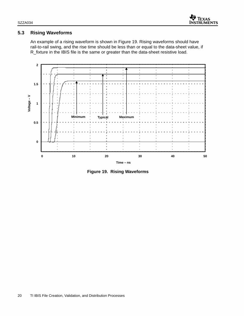
5.3 Rising Waveforms
An example of a rising waveform is shown in Figure 19. Rising waveforms should haverail-to-rail swing, and the rise time should be less than or equal to the data-sheet value, ifR_fixture in the IBIS file is the same or greater than the data-sheet resistive load.
2
1
0 10 20 30 40 50
Minimum MaximumTypical
Time – ns
Vo
ltag
e –
V
1.5
0
0.5
Figure 19. Rising Waveforms

SZZA034
21 TI IBIS File Creation, Validation, and Distribution Processes
5.4 Falling Waveforms
An example of a falling waveform is shown in Figure 20. Falling waveforms should have therail-to-rail swing, and the fall time should be less than or equal to the data-sheet value, ifR_fixture in the IBIS file is the same or greater than the data-sheet resistive load.
2
1
0 10 20 30 40 50
Minimum
Maximum
Typical
Time – ns
Vo
ltag
e –
V
1.5
0
0.5
Figure 20. Falling Waveforms

SZZA034
22 TI IBIS File Creation, Validation, and Distribution Processes
5.5 Ground-Clamp Waveforms
An example of the ground-clamp waveforms is shown in Figure 21. Some devices may have adiode connected between the input and ground or between the output and ground.Ground-clamp waveforms describe the V-I characteristics of those diodes. Sometimes there areVik-Iik data in a data sheet. In that case, the absolute magnitude of ground-clamp current at V = Vik should be equal to or greater than Iik. For example, if Vik= –1.2 V and Iik = –18 mA, onthe waveform at V = Vik, the absolute magnitude of the current should be greater than or equalto 18 mA.
–100
–1 0 1
Minimum
Maximum
Typical
0
–300
–200
VIK – V
I
= m
AIK
–1.2 V, –125 mA
Figure 21. Ground-Clamp Waveforms

SZZA034
23 TI IBIS File Creation, Validation, and Distribution Processes
5.6 Bus-Hold Behavior in Ground-Clamp Data
If the device has bus hold at the input, the input ground-clamp waveforms should be an S shapein the voltage range between 0 and VCC (see Figure 22). The voltage/current relationship shouldmatch the data-sheet Vi and Ii(hold) data. If the data sheet is specified at Vi = 0.8 V, minimumIi(hold) 75 µA, the current at V = 0.8 V on the ground-clamp waveform should be at least 75 µA.
500
0
0 1 2 3
Minimum
Maximum
Typical
250
–500
–250
VI – V
=
AI(
ho
ld)
0.8 V, 80 A
I
Figure 22. Bus-Hold Behavior in Ground-Clamp Data

SZZA034
24 TI IBIS File Creation, Validation, and Distribution Processes
5.7 Power-Clamp Waveforms
An example of power-clamp waveforms is shown in Figure 23. Some devices may have a diodeconnected between the input and VCC or between the output and VCC. If the device has a diode,the power-clamp waveform should exhibit the V-I characteristics of the diode.
60
20
–1.5 –1 0
40
0
Vik – V
–0.5
Minimum
Maximum
Typical
I =
mA
ik
Figure 23. Power-Clamp Waveforms
6 IBIS File Warnings and Errors
The IBIS file is checked using a parser to ensure that the syntax is correct. This parser is calledIBISCHK and can be downloaded from the official IBIS homepage. In the following paragraphs,some common warnings and errors are discussed, along with the reasons for those warningsand errors. Validation ensures that there is no error and all warnings are documented in thenotes section of IBIS file. In case of any warning or error, customers can consult the notessection in IBIS file and contact TI customer service.
• Some warnings may be generated due to device characteristics. The following are someexamples.
– WARNING (line n0) - GND Clamp Minimum data is non-monotonic.Non-monotonic data in ground-clamp may be due to special circuits. For example, due tothe bus-hold circuit, a ground-clamp waveform can exhibit non-monotonicity. Thereshould be a note in the notes section of the IBIS file explaining the cause ofnon-monotonicity.
– WARNING (line n1) - Pullup Minimum data is non-monotonic.Non-monotonic data in pullup may be due to a damping resistor, an over-voltageprotection circuit, or dynamic output control circuit. There should be a note in the notessection of the IBIS file explaining the cause of non-monotonicity.

SZZA034
25 TI IBIS File Creation, Validation, and Distribution Processes
– WARNING (line n2) - Pulldown Minimum data is non-monotonic.
Non-monotonic data in pulldown may be due to the dynamic output control circuit or anyfeedback circuit at the output. There should be a note in the notes section of the IBIS fileexplaining the cause of non-monotonicity.
• The following are some examples of warnings and errors that may be generated due toinaccurate IBIS data or incorrect syntax.
– WARNING (line n1) – Typ value is not in between Min and Max.
Package typical data may be wrong.
– ERROR – Component ’ALVCH16373_DGG’: Model ’ALVCH16373_OUT’ for Pin ’2’ notdefined.
The model for pin 2 in the pin section of the IBIS file is not defined in the IBIS file.
– ERROR – Model ’ALVCH16373_IN_33’ in Model Selector ’ALVCH16373_IN’ is notdefined in the file.
The model described in the model section under the “Model Selector” keyword is notdefined in the IBIS file.
– WARNING – Model ’ALVCH16373_LEIN_25’: Model_type ’Input’ must have Vinl set.
– WARNING – Model ’ALVCH16373_LEIN_25’: Model_type ’Input’ must have Vinh set.
The threshold parameter value (Vil and Vih in the datasheet) is missing from the inputmodel.
– WARNING – Model ’ALVCH16373_OUT_33’: TYP VI curves cannot drive through Vmeas = 1.5 V given load Rref = 5 ohms to Vref = 0 V.
This warning is generated when the pullup and pulldown current is not enough to drivethe load Rref up to Vmeas. Rref may be too small or Vmeas may be too high. If these arecorrect, but the warning remains, then the pullup and pulldown data may be incorrect.V–T data, if not allowed to settle down to a stable value, can generate this warning.
– WARNING – Model ‘ALVCH16373_OUT_33’: Pulldown has Decreasing Current.
The pulldown characteristics may be wrong. Pulldown should be increasing fromnegative voltage up to positive voltage. Simulation setup may be wrong.
– ERROR (line n2) – Exceeds 80 characters.
In an IBIS file, the total number of characters in a line should not exceed 80. Most often,this error is due to difference in end-of-line characters in a different platform. Forexample, an IBIS file created in the windows platform may have this error if it isdownloaded in the UNIX platform, as UNIX adds an end-of-line character at the end ofeach line in the IBIS file. The file can be converted to use in UNIX by ‘dos2unix’command.

SZZA034
26 TI IBIS File Creation, Validation, and Distribution Processes
– ERROR – Model ‘ALVCH16373_OUT_33’: The [Falling Waveform] with [R_fixture]=500Ohms and [V_fixture_min]=3V has MIN column DC endpoints of 0.55V and 3.00v, but anequivalent load applied to the model’s I–V tables yields different voltages (0.05V and3.00V), a difference of 963.74% and 0.01%, respectively.
The error is due to dc and ac data mismatch. The end point of the voltage-time data isnot the same as the dc data. For example, if the end point in the falling waveform is 0.55,then with R_fixture = 500 the current through R_fixture is determined. This current shouldrepresent the same voltage of 0.55 in the pulldown table. Most of the time this warning isgenerated when the simulation data are not taken for a sufficient time, i.e., until thevoltage waveform settled to a stable value. Sometimes, the warning may be generatedbecause the rising and falling waveform does not contain the full rail-to-rail switching.
If the percentage difference in voltage is less than a certain value, the error can come upas a warning. If the difference is negligible it does not significantly affect the accuracy. AnIBIS model created from an actual laboratory measurement can cause this warning.
– ERROR (line n3) – File name opened ’scem259.ibs’ not the same as File_name’sn74auc16245.ibs’
The name of the IBIS file should be the same name as described under “File Name”keyword in the IBIS file.
TI provides two different formats of the IBIS file, one with the .ibs extension and the otherwith the zip extension. The .ibs file has to be renamed similar to the file name describedunder (File Name) keyword in the IBIS file. The .zip file is the compressed version of the.ibs file. It can be uncompressed and the IBIS file can be used directly without renamingthe file.
7 IBIS File Distribution
If the IBIS model passes validation, it is sent to an external TI website. IBIS models can beobtained by accessing http://www.ti.com.
8 Resources
The IBIS open forum is a working group of the EIA association and, as such is responsible forthe official IBIS specification. The official website for provides information on IBIS, articles, freetools, and models.
9 References1. Introduction to IBIS Models – Arpad Muranyi, Signal Integrity Engineering, Intel Corporation.
2. I/O Buffer Information Specification, Version 3.2, IBIS Committee.
3. I/O Buffer Modeling Cookbook, IBIS Open Forum.
4. Star-HSPICE Manual, Release 1999.2, Avanti Corporation.
5. Innoveda Visual IBIS Editor, Version 3, www.innoveda.com

SZZA034
27 Using IBIS Model in HSPICE Simulation
Appendix A Using IBIS Model in HSPICE Simulation*An IBIS test file.
*********|*********|*********|*********|*********|*********|********|*********|
.OPTIONS search=’./’
.OPTIONS POST=2 $ Enables HSPLOT interface
.OPTIONS ACCT OPTS $ Prints stats & option values used
.OPTIONS SPICE=1 $ Forces Berkeley compatibility
.OPTIONS GMIN=1E–10 $ Lowest allowable conductance values
.OPTIONS GMINDC=1E–10 $ A conductance in parallel w/ PN junctions
.OPTIONS ITL1=400 $ Maximum DC iteration limit
.OPTIONS ITL4=40 $ Maximum transient iterations/timestep
.OPTIONS ITL5=0 $ No limit to total transient iterations
.TEMP 25 $ Nominal temperature
.OPTIONS LIST NODE PROBE
*********************TYPICAL CONDITION**********************
*********DRIVER***********************
b_io *Buffer call –––must start with ”b”*+nd_pu *Power supply to pullup*+nd_pd *GND supply to pulldown*+nd_out *Output node*+nd_in *Input node –––A voltage source must be connected+nd_en_driver *Enable input**+v_out_of_in *This is used by the hspice–– no voltage source should
*be connected to this node. This is used when the I/O*model works as an input model. This voltage source*can be monitored to see when*the input signal crosses the*Vinl and Vinh level. This voltage source produces a 1*or 0 based on the input signal.
+nd_pc *power supply to power clamp*+nd_gc *GND supply to ground clamp*+file=’sn74lvc245a.ibs’ *name of the ibis file. The name of the ibis file
*should match the file name under the ’File Name’*keyword in the IBIS file
+model=’LVC245A_IO_33 *Model name*+typ=typ *typical,min or max condition**+power=on *power on–hspice will take the power from Ibis file,
*If off then connect voltage source to*pullup,pulldown,gnd_clamp,power_clamp
+buffer=3 *buffer type 3 for I/O ***+xv_pu=nd_state_pu *These two nodes are used to monitor exactly how the*+xv_pd=nd_state_pd *transition is taking place. The state of these two
*node changes from 0 to 1 or vice versa during the*transition.
+interpol=1 *1=linear, 2=quadratic bi–spline. TI uses linear*interpolation when creating IBIS file
+ramp_fwf=2 *Defines which falling waveform data to use*If 0 then uses the dv/dt_f data, default 0*If 1 then uses the first falling waveform data*If 2 then uses both sets of falling waveform data
+ramp_rwf=2 *Defines which rising waveform data to use*If 0 then uses the dv/dt_r data, default 0*If 1 then uses the first rising waveform data and*If 2 then both sets of rising waveform data and
*+rwf_tune= *Tuning parameter. Used when ramp_rwf=0 or 1. This*parameter is a value between 0 and 1 and used in*conjunction with dv/dt_r in the IBIS model to*determine the time when the pulldown circuit*switches *from ON to OFF. Use ramp_rwf=2 and this

SZZA034
28 Using IBIS Model in HSPICE Simulation
*parameter is unused.
*+fwf_tune= *Tuning parameter. Used when ramp_fwf=0 or 1. This*parameter is a value between 0 and 1 and used in*conjunction with dv/dt_f in the IBIS model to*determine the time when the pullup circuit*switches from ON to OFF. Use ramp_fwf=2 and this*is unused
*+nowarn *suppresses warning messages
****PKG CONNECTION***CPKG nd_out 0 2.19870E–13*HSPICE simulator does not connect the pkg data withLPKG driver_out cen 4.31600E–09*the IBIS model. Connect the package R, L and C data.RPKG cen nd_out 6.00971E–02
**********************************************
****LOAD ****TRANSMISSION LINE*****
TLOAD driver_out 0 lineend 0 ZO=50 TD=5.81ns L=1.3769
****TERMINATION*****
Rpu lineend tt 50Vterm tt 0 dc 3.3
.tran 0.1ns 245ns
*********TRANSIENT ANALYSIS**********
Vin nd_in 0 PULSE 0 1 6.07n 0n 0n 123n 240n
Ven1 nd_en_driver 0 dc 0v **ACTIVE LOW***
.print tran V(driver_out) V(nd_in)
****************************************
.END

IMPORTANT NOTICE
Texas Instruments Incorporated and its subsidiaries (TI) reserve the right to make corrections, modifications,enhancements, improvements, and other changes to its products and services at any time and to discontinueany product or service without notice. Customers should obtain the latest relevant information before placingorders and should verify that such information is current and complete. All products are sold subject to TI’s termsand conditions of sale supplied at the time of order acknowledgment.
TI warrants performance of its hardware products to the specifications applicable at the time of sale inaccordance with TI’s standard warranty. Testing and other quality control techniques are used to the extent TIdeems necessary to support this warranty. Except where mandated by government requirements, testing of allparameters of each product is not necessarily performed.
TI assumes no liability for applications assistance or customer product design. Customers are responsible fortheir products and applications using TI components. To minimize the risks associated with customer productsand applications, customers should provide adequate design and operating safeguards.
TI does not warrant or represent that any license, either express or implied, is granted under any TI patent right,copyright, mask work right, or other TI intellectual property right relating to any combination, machine, or processin which TI products or services are used. Information published by TI regarding third–party products or servicesdoes not constitute a license from TI to use such products or services or a warranty or endorsement thereof.Use of such information may require a license from a third party under the patents or other intellectual propertyof the third party, or a license from TI under the patents or other intellectual property of TI.
Reproduction of information in TI data books or data sheets is permissible only if reproduction is withoutalteration and is accompanied by all associated warranties, conditions, limitations, and notices. Reproductionof this information with alteration is an unfair and deceptive business practice. TI is not responsible or liable forsuch altered documentation.
Resale of TI products or services with statements different from or beyond the parameters stated by TI for thatproduct or service voids all express and any implied warranties for the associated TI product or service andis an unfair and deceptive business practice. TI is not responsible or liable for any such statements.
Mailing Address:
Texas InstrumentsPost Office Box 655303Dallas, Texas 75265
Copyright 2002, Texas Instruments Incorporated