The Fundamental Hardware Elements and Options of Digital ...
41
University of Central Florida University of Central Florida STARS STARS Retrospective Theses and Dissertations Fall 1983 The Fundamental Hardware Elements and Options of Digital The Fundamental Hardware Elements and Options of Digital Signal Processing Signal Processing Mark A. Hemmerlein University of Central Florida Part of the Engineering Commons Find similar works at: https://stars.library.ucf.edu/rtd University of Central Florida Libraries http://library.ucf.edu This Masters Thesis (Open Access) is brought to you for free and open access by STARS. It has been accepted for inclusion in Retrospective Theses and Dissertations by an authorized administrator of STARS. For more information, please contact [email protected]. STARS Citation STARS Citation Hemmerlein, Mark A., "The Fundamental Hardware Elements and Options of Digital Signal Processing" (1983). Retrospective Theses and Dissertations. 686. https://stars.library.ucf.edu/rtd/686
Transcript of The Fundamental Hardware Elements and Options of Digital ...
University of Central Florida University of Central Florida
STARS STARS
Retrospective Theses and Dissertations
Fall 1983
The Fundamental Hardware Elements and Options of Digital The Fundamental Hardware Elements and Options of Digital
Signal Processing Signal Processing
Mark A. Hemmerlein University of Central Florida
Part of the Engineering Commons
Find similar works at: https://stars.library.ucf.edu/rtd
University of Central Florida Libraries http://library.ucf.edu
This Masters Thesis (Open Access) is brought to you for free and open access by STARS. It has been accepted for
inclusion in Retrospective Theses and Dissertations by an authorized administrator of STARS. For more information,
please contact [email protected].
STARS Citation STARS Citation Hemmerlein, Mark A., "The Fundamental Hardware Elements and Options of Digital Signal Processing" (1983). Retrospective Theses and Dissertations. 686. https://stars.library.ucf.edu/rtd/686
THE FUNDAMENTAL HARDWA..R.E ELEMEHTS AND OPTIONS OF DIGIT1'.i..1 SIGNAL PROCESSING
BY
JYJ.AR.T{ A . HEMMERLEI N B. S.E., University of Central Florida, 1980
RESEARCH REPORT
Submitted in partial fulfillment of the requirements for the degree of Master of Science in Ehgineering
in the Graduate Studies Program of the College of Engineering University of Central Florida
Orlando, Florida
Fall Term 1983
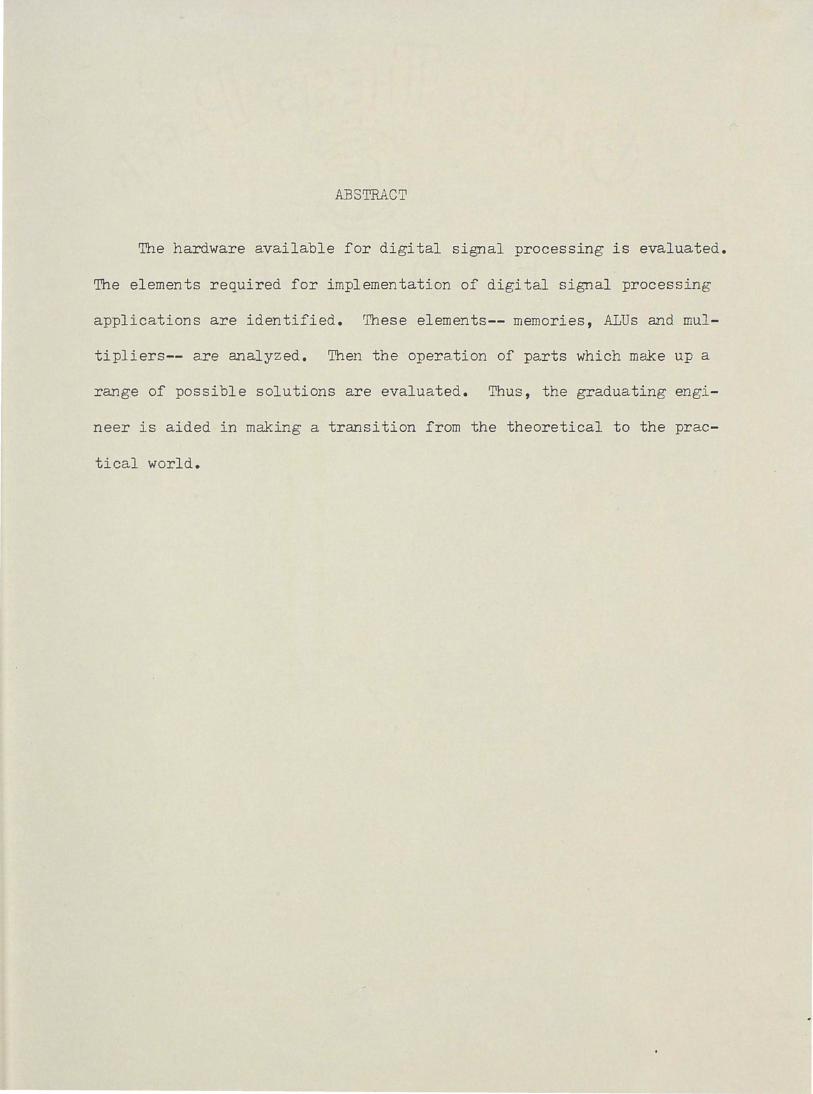
ABSTRACT
The hardware available for digital signal processing is evaluated.
The elements required for implementation of digital signal processing
applications are identified. These elements-- memories, ALUs and mul
tipliers-- are analyzed. Then the operation of parts which make up a
range of possible solutions are evaluated. Thus, the graduating engi
neer is aided in making a transition from the theoretical to the prac
tical world.
TABLE OF CONTENTS
LIST OF TABL~S • • • • • • • • • • • • • • • • • • • • • • • •
LIST OF FIGURES • • • • • • • • •
I INTRODUCTION • • • • • • • • • • •
II BACKGROill.Jl) • • • • • • • • •
III - FUNDJ\MENTAL EL:E!MENTS • • • • • • •
1. 2. 3. 4.
Registers and Memories Addition • • • • Multiplication Di vision • •
• • •
• •
• • •
• • • • • • • • • • • • •
IV - H"PLEMENTATIONS • • • • • •
1. 2. 3. 4. 5.
Correlation/Convolution • • • • • • Fixed Instruction Set Microprocessor Bit Slice Processor • • • • • • • Single Chip Signal Processors • • • Comparison of Implementations • •
• • •
• • • •
• •
•
•
• •
• • • • • • • • •
• • • • • • •
• • • • • • •
• • • • • •
• • • • • • • • • • • • • • • • • • • •
• • • • • •
• • • • • • •
• • • • • • • • • •
• • • • • • • • • • • •
• • • • • •
V - CONCLUSION • • • • • • • • • • • • • • • •
REFERENCES • • • • • • • • • • • • • • • • •
iii
iv
v
1
2
3
3 8
11 14
16
16 18 22 28 31
34
35
LIST OF TABLES
1 . Data Path Delay 16 Bit Ripple Carry Adder/Subtracter • • • • •
2. Design Cost and Time Considerations • • • • • • • • • • • • •
iv
12
33
LI ST OF FIGURES
1. 4096 Bit Static Random Access Memory • • . . • • . • • . . 5 2. 16,384 :Bit Dynamic Random Access Memory • • • • . • . . • . 5 3. 8192 Bit PRON • . • • . • • • . . • . . . . . . • . • . . 7 4. 16 Word by 4 Bit Dual Port R.AJl.i . . • • • . . . • • . • 7 5. FIFO Memory • • • • . • . • • • . . • • . • . . • . . 9 6. Cascaded Full Adder Cells Connected as a Four Bit
Ri pple Carry Adder • . • • • • . . • . . • • • . . • . 10 7. Connection of 16 :Bit ALU Using Ripple Carry • • • • . • . • 10 8 . Full Lookahead Carry 16 Bit Adder • • • . • . . . • • • . • 12 9 . Clocked Add-shift Multiplier . . • . • . • • • • • • • • • 13
10 . Structure for Array Multiplier • . • . • • • • . . • • 13 11. Fixed Poin t Binary Division • • . • • • • • • • • . • 15 12. Di gi tal Correlator • • • • . • • • • • • • • • • • • • . . 17 13. Sam ple Output of Di gital Correlator • • . • • • . . • . . . 17 14 . Convolution Using a Digital Correlator • • . . • • . • • . 19 15. 8085 Yri croprocessor System Using 74S508 to Provide
a Hardware Multiply • • • • • • . . . . • . • . • . • • • . 20 16. Routine for 8085 Software Multiply • • . • . • • • • • • • 21 17. Routine for 8085/74S508 Multiply • . . . • • . • • • • • • 21 18 . Single Precision Format for 8232 Floating Point
Number • • . • . • • • • • . • . . . . • . • • • . . • • • 22 19 . Simple ~li croprograrnm ed Architecture . . . • . . . . • . • . 23 20. Pipelining Bit Slice Architecture . • . • • • . . • . 23 21. AM2903 ALU • • . . • • . • • ·• . . • . • . . • • . • • • • 25 22. Interconnections and Microcode Algorithm for 16
Bit Ri pple Carry Multiply • • • • • • • • . • • • • • • • • 26 23. Array Processor • • • • • • • • . • • • • • • . • • • . • . 27 24. 2920 Signal Processor • • . . . . • • • • • . • • • . . • • 29 25. TMS320 Im pl emen ta ti on for FIR Filter • • • . • • • . . • • 30 26. Complexity vs. Throughput . • • • • • . . • • • . • • • • • 32
v
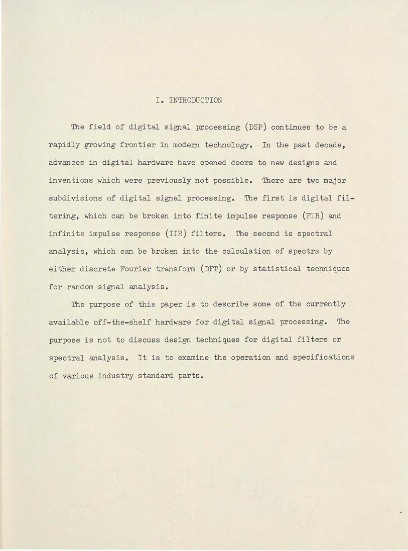
I. INTRODUCTION
The field of digital signal processing (DSP) continues to be a
rapidly growing frontier in modern technology. In the past decade,
advances in digital hardware have opened doors to new designs and
inventions which were previously not possible. There are two major
subdivisions of digital signal processing. The first is digital fil
tering, which can be broken into finite impulse response (FI R) and
infinite impulse response (IIR) filters. The second is spectral
analysis, which can be broken into the calculation of spectra by
either discrete Fourier transform (DFT) or by statistical techniques
for random signal analysis.
The purpose of this paper is to describe some of the currently
available off-the-shelf hardware for digital signal processing. 'Ihe
purpose is not to discuss design techniques for digital filters or
spectral analysis. It is to examine the operation and specifications
of various industry standard parts.
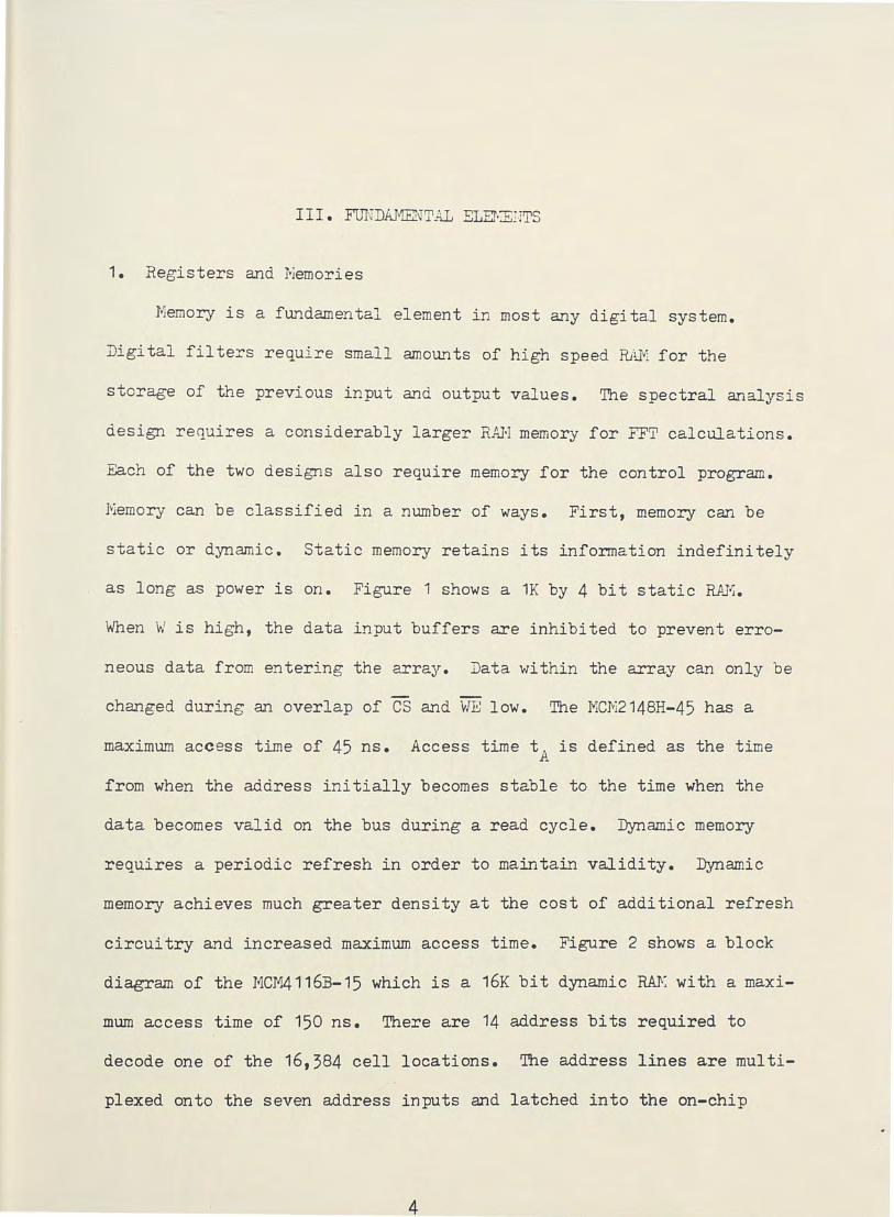
II. :BACKG~omrn
The primary arithmetic operations for digital signal processing
are addition and multiplication. Consider a~ example from the first
major subdivision of digital signal processing-- digital filtering.
The second order filter model below requires 5 multiplications and
4 additions for each value of y(n) •
. zilso consider an exa~ple from the second major subgroup of digital
signal processing. The fast Fourier transform (FFT), which is at the
heart of most spectral analysis applications, is used to deterLline the
discrete Fourier transform (DFT) of the finite duration sequence x(n)
of length N.
N-1 [ 2 ~ X(k)=Ex(n)exp- N71 nk j
n=O
where k = 0, 1 , 2. • • N-1
In order to perform this spectral analysis, ~ log2I-~ complex mul tipli
cations and N log2N complex ad.di tions are required.
The four primary implementations to be considered for the above
digital signal processing applications are (1) hardwired logic,
including SSI/~IBI, semi-custom and custom integrated circuits; (2) 8
or 16 bit general purpose microprocessors; (3) single chip signal
processors; and (4) microprogrammable bit slice architectures.
2
There are some major tradeoffs for these four implementations.
If high speed, critical instruction sets or long word lengths are
required, the 8 or 16 bit standard microprocessors cannot be used.
3
If parts count and design time must be minimized, then the micropro
cessor-based design is preferred. Yet, if a system requires high speed
and long word lengths and still must be easily upgraded, then the bit
slice microprogrammed design might be preferred. It can usually be
changed by replacement of a PRm1: , which is much easier than cha'1ging
hardwired logic.
Thus, the balance of the paper discusses the memories, adders,
multipliers and controllers available for digital signal processing •
..
III. FUNDAMENTAL ELD:E:i·JTS
1. Registers and 1·1emories
r~emory is a fundamental element in most any digital system.
Digital filters requi re small amounts of high speed R.iU!i for the
storage of the previous input and output values. The spectral analysis
design requires a considerably larger R.Af·l memory for FFT calculations.
Each of the two designs also require memory for the control program.
Nemory can be classified in a number of ways. First, memory can be
static or dynamic. Static memory retains its information indefinitely
as long as power is on. Figure 1 shows a 1K by 4 bit static RAJ'i .
When V.I is high, the data input buffers are inhibited to prevent erro
neous data from entering the array. Data within the array can only be
changed during an overlap of CS and WE low. The MCM2148H-45 has a
maximum access time of 45 ns. Access time tA is defined as the time
from when the address initially becomes stable to the time when the
data becomes valid on the bus during a read cycle. Dynamic memory
requires a periodic refresh in order to maintain validity. Dynamic
memory achieves much greater density at the cost of additional refresh
circuitry and increased maximum access time. Figure 2 shows a block
diagram of the MCM4116B-15 which is a 16K bit dynamic RA1': with a maxi
mum access time of 150 ns. There are 14 address bits required to
decode one of the 16,384 cell locations. The address lines are multi
plexed onto the seven address inputs and latched into the on-chip
4
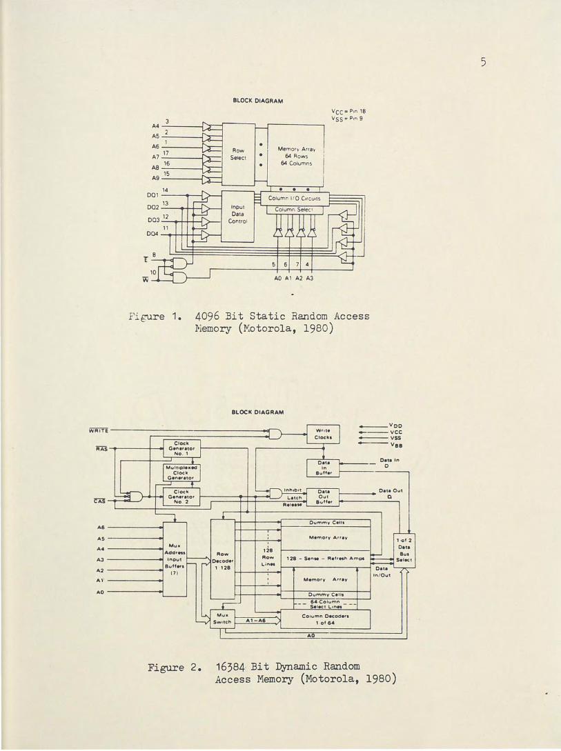
Fig-u.re 1.
R"As-------..
AS-------,..
A<I -------- Mux Addrns
AJ-------- Input
Buffers A2 -------- ( 7 )
A\
AO--------
BLOCK DIAGRAM
Row Select
Input Data
Control
• • •
Memory Array 64 Rows
64 Columns
AO Al A2 A3
Vcc=P1n 1s v 55 =Pin 9
4096 Bit Static Random Access Memory (Motorola, 1980)
BLOCK DIAGRAM
Row
Wrote
Clocks
Data In
Buffer
----"DD ----vcc ----vss
V99
Data In 0
Data Out
Buffer
1-------- Oat~ Out
Dummy Cells
Memory Arrav
Memory Array
Dummy Cells
6<1 ·Column Select L1nti'I
Co1umn Decodars
1 ·0f ·6•
AO
1 ·Of 2 Data
Figure 2. 16384 Bit Dynamic Random Access Memory (Motorola, 1980)
5
6
latches. The first clock, the row address strobe (RAS), latches the
seven row address bits into the chip. The second clock, the column
address strobe (CAS), latches the seven column address bits into the
chip. Data to be written into a selected cell is then latched into an
on-chip register by a combination of WRITE and CAS while RAS is active.
Data is to be retrieved from the selected cell in a read cycle by
maintaining WRITE in the inactive state throughout the portion of the
memory cycle in which CAS is active low.
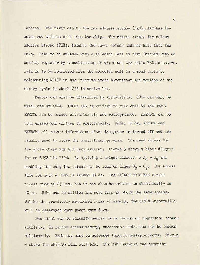
Memory can also be classified by wri tabili ty. RO:Ms can only be
read, not written. PROMs can be written to only once by the user.
EPROMs can be erased ul travioletly and reprogrammed. EEPR01'1s can be
both erased and written to electrically. ROMs, PRO~IB, EPRO~IB and
~'PROMs all retain information after the power is turned off and are
usually used to store the controlling program. The read access for
the above chips are all very similar. Figure 3 shows a block diagram
for an 8192 bit PROM. By applying a unique address to A0 - ~ and
enabling the chip the output can be read on lines o0 - o7• The access
time for such a PROM is around 60 ns. The EEPROM 2816 has a read
access time of 250 ns, but it can also be written to electrically in
10 ms. RAMs can be written and read from at about the same speeds.
Unlike the previously mentioned forms of memory, the R.AI1's information
will be destroyed when power goes down.
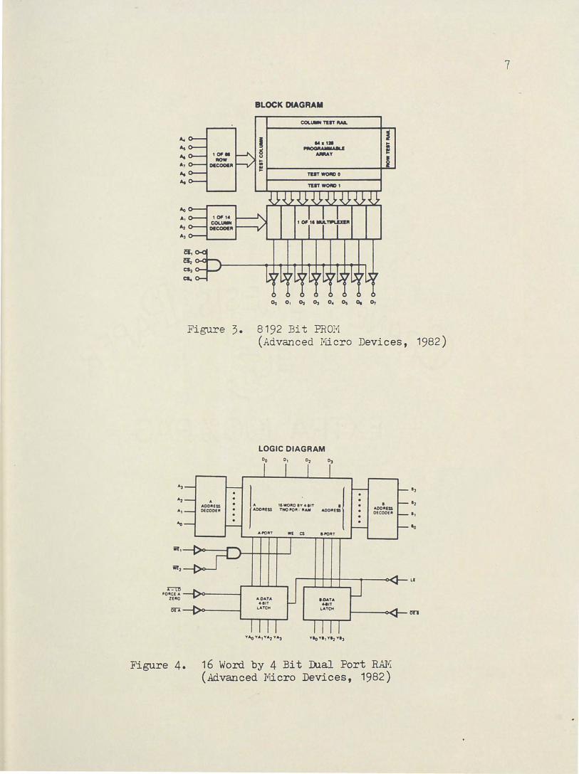
The final way to classify memory is by random or sequential acces
sibility. In random access memory, successive addresses can be chosen
arbitrarily. RAMs may also be accessed through multiple ports. Figure
4 shows the AM29705 Dual Port RAM. The RAM features two separate
.. ~ .. 1 OF•
"°w A7 DeCOOER .. .. Ao A1 1Of14
~ COL..-t
DeCODER
AJ
Ci,
~ cs, ca..
Figure 3.
"1
x-:-rn
" ADDllESS DECODE II
FOllCE A --t~oo-----1 ZEllO
on --t~-0-----1
BLOCK DIAGRAM
COL..-t TUT RAIL
I i ... ,. = 8 ARRAY I!! • ~ i • Ill
~
TUTWON>O
~.,.WON) 1
8192 Bit PROM (Advanced ~licro Devices, 1982)
LOGIC DIAGRAM Do
" ADDllESS
A.l'()llT
A.OAT.A 4·81T
LATCH
D1 D2 D3
16·WOllD 8Y 4·llT • 1'#0-POA • 11.Alll ADDllESS
WE cs 8.l'OllT
13
• 82 ADDllESS DECOOEll 81
Bo
t----OC~I-- CJR
Figure 4. 16 Word by 4 Bit fual Port RAJ~ (Advanced Micro Devices, 1982)
7
8
output ports such that any two 4 bit words can be read from these
outputs simultaneously. In sequential memory, adjacent bits appear at
the output in sequence. Sequential memories take the fonn of first-
in-first-out (FIFO) memories and shift registers. FIFOs may be util-
ized whenever two variable speed processes must be interfaced or a
number of samples must be taken b~fore processing may begin (FFT proc-
essing). Figure 5 shows the block diagram for the c5/c67401/A FIFO
memory. Data enters when the shift in (SI) input goes high. Data
exits when the shift out (so) input goes high. The outputs input
ready (IR) and output ready (OR) are low when the memory is full or
empty respectively.
2. Addition
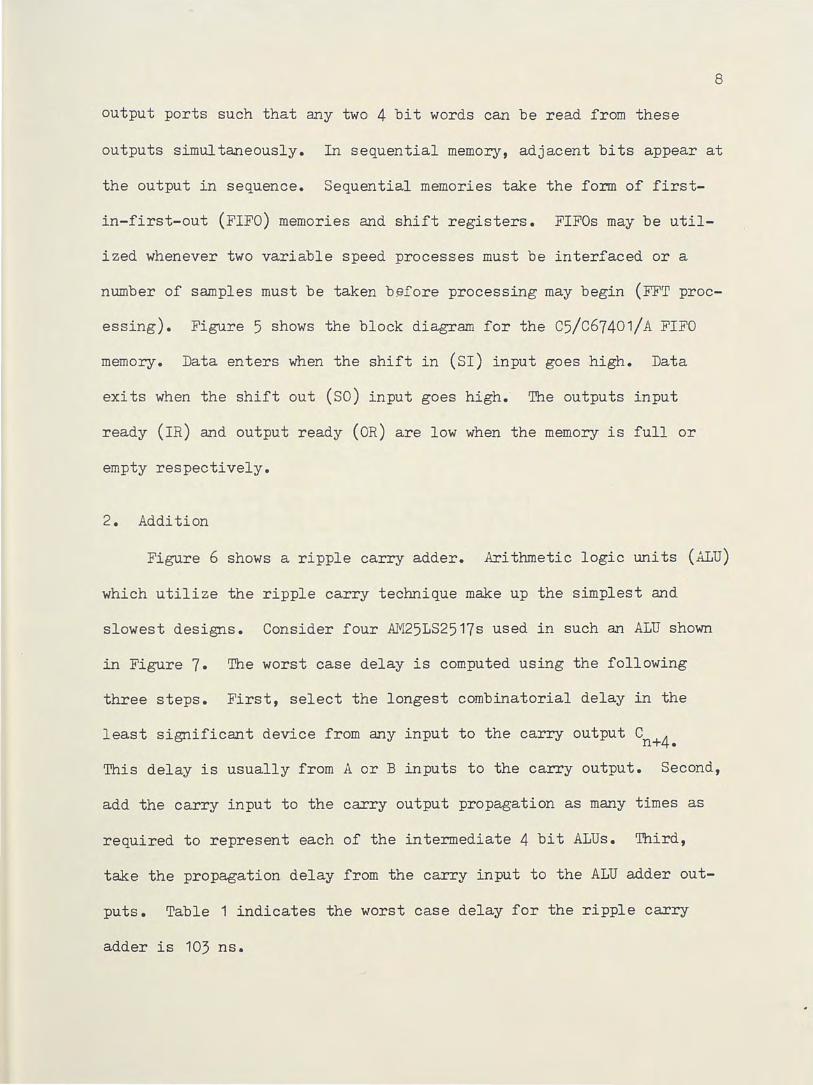
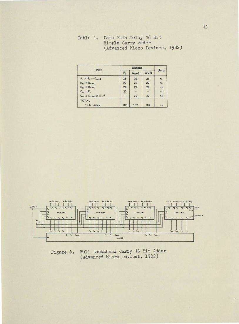
Figure 6 shows a ripple carry adder. Arithmetic logic units (ALU)
which utilize the ripple carry technique make up the simplest and
slowest designs. Consider four .AM25LS2517s used in such an ALU shown
in Figure 7. The worst case delay is computed using the following
three steps. First, select the longest combinatorial delay in the
least significant device from any input to the carry output C n+4.
This delay is usually from A or B inputs to the carry output. Second,
add the carry input to the ca:rry output propagation as many times as
required to represent each of the intermediate 4 bit ALUs. Third,
take the propagation delay from the carry input to the ALU adder out-
puts. Table 1 indicates the worst case delay for the ripple ca:rry
adder is 103 ns.

Block Diagram•
INPUT "fAOY
CS/C87.a1/ A Mx4
Figure 5. First-In-First-Out (FIFO) Memory (Monolithic Memories, 1981)
0 /
C1N Vo Xo
A
Co
So
Figure 6.
v, x, V2 X2 V3 X3
c B A A A
Co Co Co
s, 52 SJ CoUT
Cascaded Full Adder Cells Connected as a 4 Bit Ripple Carry Adder (Advanced Micro Devices, 1982)
•o • ' f~ •3
Figure 7.
•• F~ <6 f 7
Connection for a 16 Bit ALU Using Ripple Carry (Advanced Yrlcro Devices, 1982)
10
11
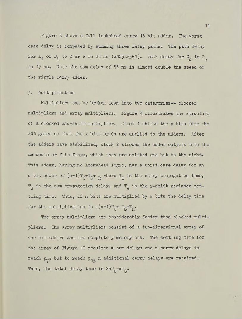
Figure 8 shows a full lookahead carry 16 bit adder. The worst
case delay is computed by summing three delay paths. The path delay
for Ai or Bi to G or Pis 26 ns (AM25LS381). Path delay for en to F3
is 19 ns. Note the sum delay of 55 ns is almost double the speed of
the ripple carry adder.
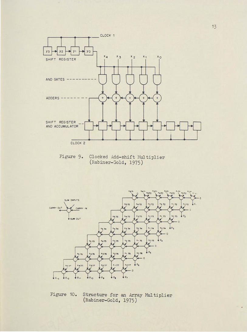
3. Multi plication
Multipliers can be broken down into two categories-- clocked
multipliers and array multipliers. Figure 9 illustrates the structure
of a clocked add-shift multiplier. Clock 1 shifts they bits into the
AND gates so that the x bits or Os are applied to the adders. After
the adders have stabilized, clock 2 strobes the adder outputs into the
accumulator flip-flops, which then are shifted one bit to the right.
This adder, having no lookahead logic, has a worst case delay for an
n bit adder of (n-1)Tc+T8+TR where TC is the ca:rry propagation time,
T8 is the sum propagation delay, and TR is the y-shift register set
tling time. Thus, if n bits are multiplied by m bits the delay time
for the multiplication is m(n-1)TC+mT8+TR.
The array multipliers are considerably faster than clocked multi
pliers. The array multipliers consist of a two-dimensional array of
one bit adders and are completely memoryless. The settling time for
the array of Figure 10 requires m sum delays and n ca:rry delays to
reach p7
; but to reach p13
n additional carry delays are required.
Thus, the total delay time is 2nTc+mT8•
'-----'C..
Figure 8.
Table 1.
Path
Aj or Bi to Cn+4
Cn to Cn+4
Cn to Cn+4
Cn t<;> Fi
Data Path Delay 16 Bit Ripple Carry Adder (Advanced Micro Devices, 1982)
Output Units'
Fi Cn+4 OVR
36 36 36 ns
22 22 22 ns
22 22 22 ns
23 - - ns
Cn to Cn+4 or OVA - 22 22 ns
TOTAL
16-bit delay 103 102 102 ns
i:, •, c,, •• l:2 '2 c,., .. _ Full Lookahead Carry 16 Bit Adder (Advanced Micro Devices, 1982)
12
CLOCK
SHIFT REGISTER x 3 x 2
AND GATES --- -- ---- -
ADDERS------ - -
SHIFT REGISTER __ AND ACCUMULATOR
CLOCK 2
Figure 9.
SUM INPUTS
CARRY O~RY 11\1
- ls~ OUT
Clocked Add-shift Multiplier (Rabiner-8-old, 1975)
Figure 10. Structure for an Array Multiplier (Rabiner-Gold, 1975)
13
14
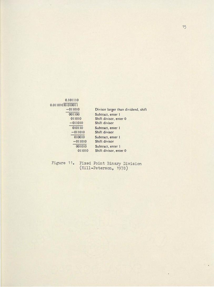
4. Division
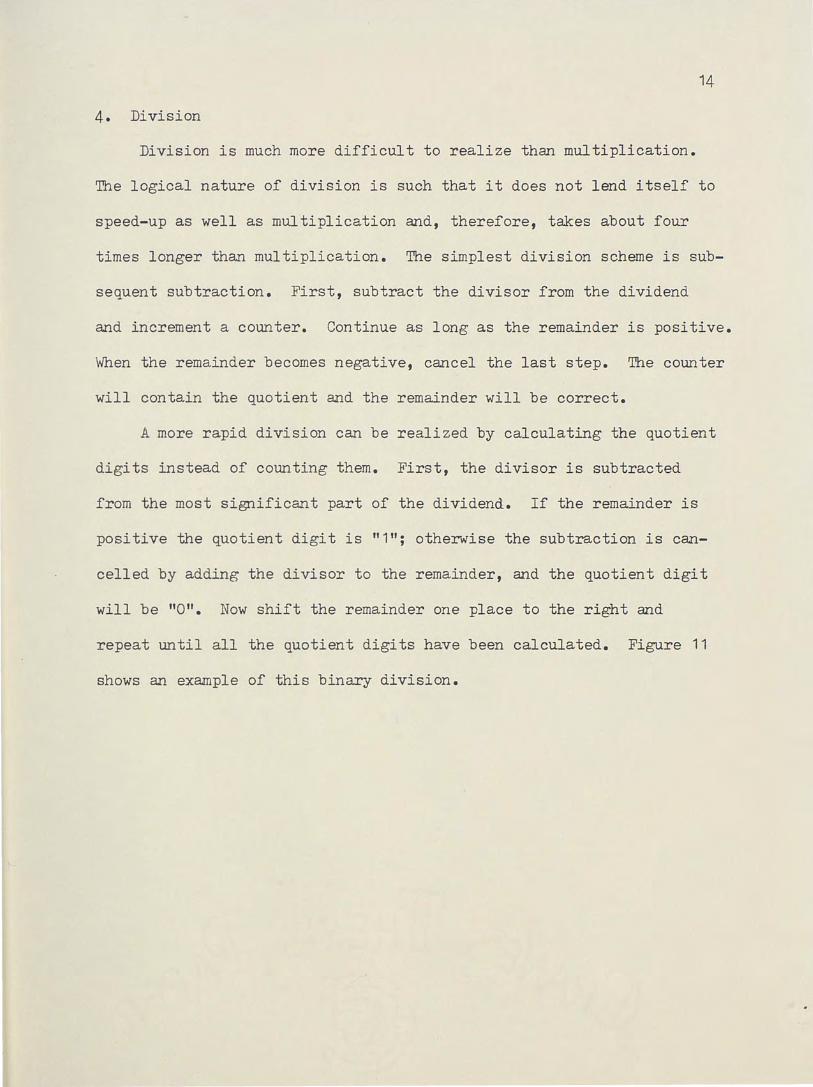
Division is much more difficult to realize than multiplication.
The logical nature of division is such that it does not lend itself to
speed-up as well as multiplication and, therefore, takes about four
times longer than multiplication. The simplest division scheme is sub
sequent subtraction. First, subtract the divisor from the dividend
and increment a counter. Continue as long as the remainder is positive.
When the remainder becomes negative, cancel the last step. The counter
will contain the quotient and the remainder will be correct.
A more rapid division can be realized by calculating the quotient
digits instead of counting them. First, the divisor is subtracted
from the most significant part of the dividend. If the remainder is
positive the quotient digit is "1"; otherwise the subtraction is can
celled by adding the divisor to the remainder, and the quotient digit
will be "0". Now shift the remainder one place to the right and
repeat until all the quotient digits have been calculated. Figure 11
shows an example of this binary division.
0.101110
0.011010)0.010011 -011010
001100 011010
-011010
010110 -011010
010010 -011010
001010 011010
Divisor larger than dividend, shift
Subtract, enter 1 Shift divisor, enter 0 Shift divisor
Subtract, enter 1 Shift divisor
Subtract, enter 1 Shift divisor
Subtract, enter 1 Shift divisor, enter 0
Figure 11. Fixed Point Binary Division (Hill-Peterson, 1978)
15
IV. IMPLEMENTATIONS
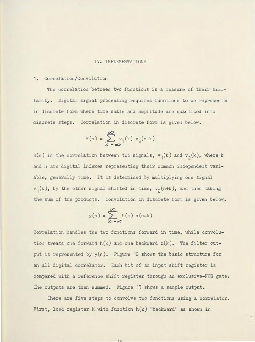
1. Correlation/Convolution
The correlation between two functions is a measure of their simi-
larity. Digital signal processing requires functions to be represented
in discrete form where time scale and amplitude are quantized into
discrete steps. Correlation in discrete form is given below.
oO
R(n) = L v 1(k) v2 (n+k) k=- 00
R(n) is the correlation between two signals, v 1(k) and v2(k), where k
and n are digital indexes representing their common independent vari-
able, generally time. It is determined by multiplying one signal
v 1(k), by the other signal shifted in time, v2(n+k), and then taking
the sum of the products. Convolution in discrete form is given below.
00
y(n) = ~ h (k) x(n-k) k=-oO
Correlation handles the two functions forward in time, while convolu-
tion treats one forward h(k) and one backward x(k). The filter out-
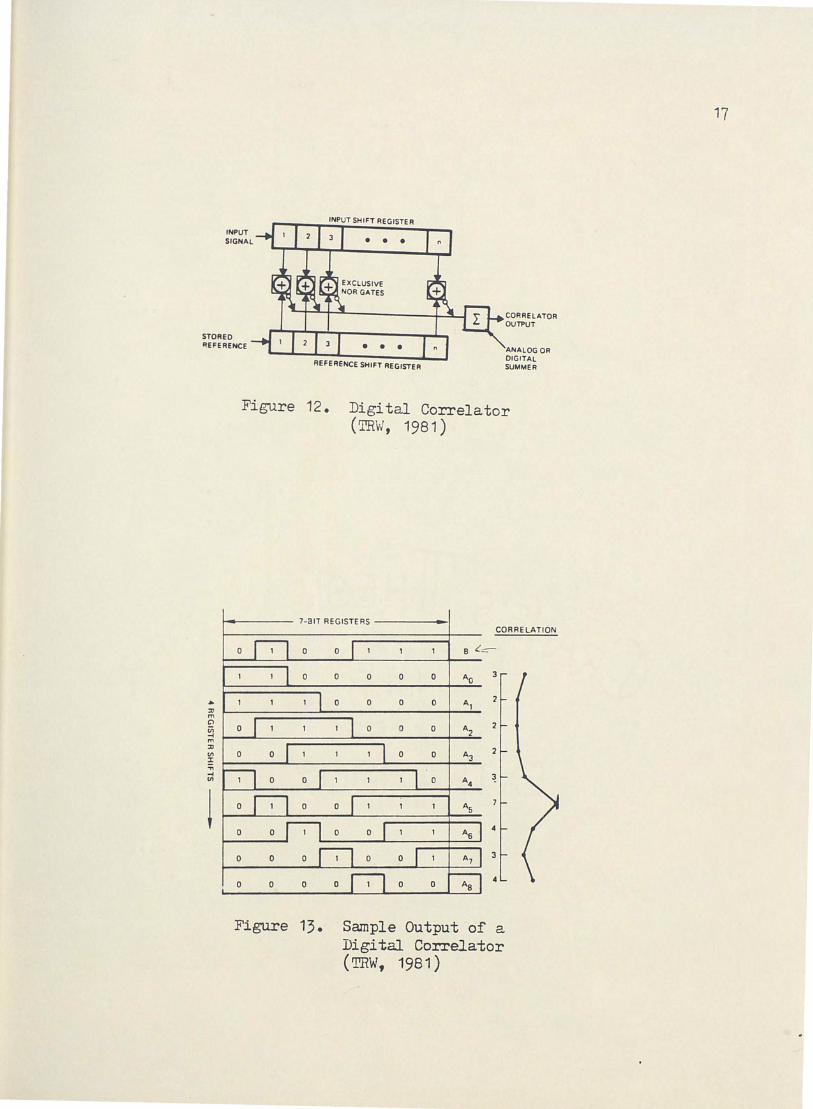
put is represented by y(n). Figure 12 shows the basic structure for
an all digital correlator. Each bit of an input shift register is
compared with a reference shift register through an exclusive-NOR gate.
The outputs are then summed. Figure 13 shows a sample output.
There are five steps to convolve two functions using a correlator.
First, load register M with function h(k) "backward" as shown in
INPUT SIGNAL
STORED REFERENCE
INPUT SHIFT REGISTER
• • •
• • •
CORRELATOR OUTPUT
REFERENCE SHIFT REGISTER
ANALOG OR DIGITAL SUMMER
Figure 12. Digital Correlator (TRW, 1981)
7-31T REGISTERS
• ::tJ m C'l
0
Vi 0 ~ ::tJ (/')
::c :;; ~ Cll
0
0
Figure 13.
0
0
0
CORRELATION
B t:_~
0 0 0 Ao 3
0 0 0 Al 2
0 0 0 A2 2
~
Sample Output of a IJigi tal Correlator (TRW, 1981)
17
18
Figure 14. Second, clock function x(k) forward through A until x 1 and
h 1 align. Third, compute the first convolution point, y 1=x1•h1
•
Fourth, advance "A" register contents one bit, and compute y2=h1x2
+h2x
1•
Fi fth, continue until the sequence is completed. The TRW TDC1023J has
a maximum bit rate of 20 MHz.
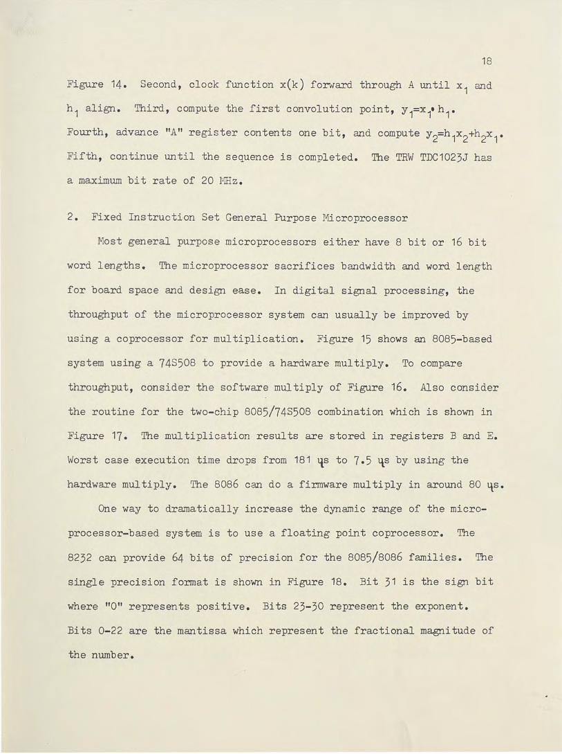
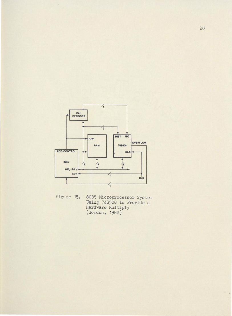
2. Fixed Instruction Set General Purpose Microprocessor
Most general purpose microprocessors either have 8 bit or 16 bit
word lengths. The microprocessor sacrifices bandwidth and word length
for board space and design ease. In di gital signal processing, the
throughput of the microprocessor system can usually be improved by
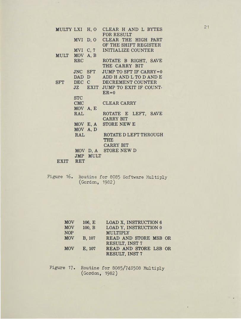
using a coprocessor for multiplication. Figure 15 shows an 8085-based
system using a 748508 to provide a hardware multiply. To compare
throughput, consider the software multiply of Figure 16. Also consider
the routine for the two-chip 8085/748508 combination which is shown in
Figure 17. The multiplication results are stored in registers Band E.
Worst case execution time drops from 181 qs to 7.5 ~s by using the
hardware multiply. The 8086 can do a firmware multiply in around 80 qs.
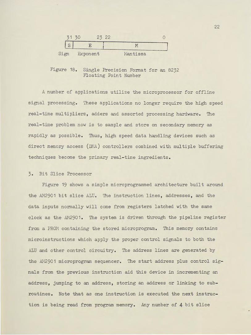
One way to dramatically increase the dynamic range of the micro-
processor-based system is to use a floating point coprocessor. The
8232 can provide 64 bits of precision for the 8085/8086 families. The
single precision format is shown in Figure 18. Bit 31 is the sign bit
where "0" represents positive. Bits 23-30 represent the exponent.
Bits 0-22 are the mantissa which represent the fractional magnitude of
the number.
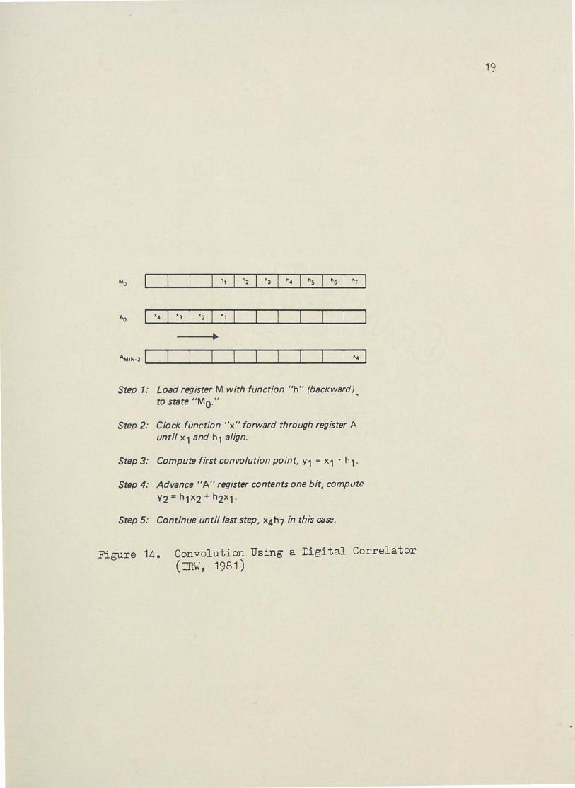
Step 1: Load register M with function "h" (backward) to state "Mo."
Step 2: Clock function "x" forward through register A until x 1 and h 1 align.
Step 3: Compute first convolution point, Y1 = x1 • hi.
Step 4: Advance "A" register contents one bit, compute v2 = hix2 + h2x1.
Step 5: Continue until last step, x4h7 in this case.
Figure 14. Convolution Using a Digital Correlator (TRW, 1981)
19
/
.... 1
PAL .. DECODER
• /
/3 i • ~
INST GO R/W
OVERFLOW RAM 1tl508
ADD/ CONTROL ~ [a · ~K f4--
• • 8085 v v v
, 8 J 8 '8
AD0-AD7 - t t --CLK / - ,, 1
CLK
/
/
Figure 15. 8085 I'licroprocessor System Using 748508 to Provide a Hardware !"iul ti ply (Gordon, 1982)
20
MULTY LXI H,O CLEAR H AND L BYTES FOR RESULT
MVI D,O CLEAR THE HIGH PART OF THE SHIFT REGISTER
MVI c, 7 INITIALIZE COUNTER MU~T MOV A,B
RRC ROTATE B RIGHT, SAVE THE CARRY BIT
JNC SFT JUMP TO SFT IF CARRY =O DAD D ADD HAND LTO DAND E
SFT DEC c DECREMENT COUNTER JZ EXIT JUMP TO EXIT IF COUNT-
ER=O STC CMC CLEAR CARRY MOV A,E RAL ROTATE E LEFT, SAVE
CARRY BIT MOV E,A STORE NEWE MOV A,D RAL ROTATE D LEFT THROUGH
THE CARRY BIT
MOV D,A STORE NEWD JMP MULT
EXIT RET
Figure 16. Routine for 8085 Software Multiply (Gordon, 1982)
MOV 106, E LOAD X, INSTRUCTION 6 MOV 100, B LOAD Y, INSTRUCTION 0 NOP MULTIPLY MOV B, 107 READ AND STORE MSB OR
RESULT, INST 7 MOV E, 107 READ AND STORE LSB OR
RESULT, INST 7
Figure 17. Routine for 8085/748508 Multiply (Gordon, 1982 )
21
31 30 23 22 0
I s I E l M
Sign Exponent liantissa
Figure 18. Single Precision Format for an 8232 Floating Point Number
A nwnber of applications utili ze the microprocessor for offline
22
signal processing. These applications no longer require the high speed
real-time multipliers, adders and assorted processing hardware. The
real-time problem now is to sample and store on secondary memory as
rapidly as possible. Thus, high speed data handling devices such as
direct memory access (D}lA ) controllers combined with multiple buffering
techniques become the primary real-time ingredients.
3. Bit Slice Processor
Figure 19 shows a simple microprogrammed architecture built around
the AJV12901 bit slice ALU. The instruction lines, addresses, and the
data inputs normally will come from registers latched with the same
clock as the AM2901. The system is driven through the pipeline register
from a PROM containing the stored microprogram. This memory contains
microinstructions which apply the proper control signals to both the
ALU and other control circuitry. The address lines are generated by
the AJvI2901 microprogram sequencer. The start address plus control sig-
nals from the previous instruction aid this device in incrementing an
address, jumping to an address, storing an address or linking to sub-
routines. Note that as one instruction is executed the next instruc-
tion is being read from program memory. Any number of 4· bit slice

OTHER ADDRESS SOURCES
a-l....-.. ()II Am2111a ()II ""'29101
Figure 19.
FROM DATA IUS
~i 1•11
INSTRUCTION I REGISTER I
OR l'LA)I ~ING I l'ROM
.. A .., ( ,,
.... "" ""J D So
S1 FE
IEOUENCEll l'V'
y C' c,,
t @
J)
... "'~ A
START ADO RESS
ADDRESS
MICROf'ROGRAM STORE
CROMll'flOMl
COf'TROL
A , 8
JUtll' ADDRESS
CLOCK
TO OTHER DEVICES
DATA IN
DATA OUT
Simple Microprogrammed Architecture (Advanced J1·iicro Devices, 1982)
CLOCK l)__r-
... v
... CONTROL ...
v LOGIC ~ROM . SS 1 l ....
STATUS I ~ REGISTER
r-..r- (M\2111) c
- -FROM DATA IUS
~i ~
I=- 1-1 DATA
I REGISTER
cc MICROl'ROGRAM -«> llTS L
{J, MEMORY
0 ' IA C' 0 c;.., ~ROM I ... -21eTOOWOROS l'tl'ELIN£ G) ..
1 I@
v H z I @
@; REGISTER A ""'2901 ARRAY OVR -
ruction currently being exec:ut8d 1 Microinst
2 SeQuen mr control tin• •l•ct aource of next m icroinstruction eddrea
3 Next m
' Next m
icrolnstruction eddrn1
ictolnstruction
I Status bits from current microinstruction
I Status bits from last microinstruction
Figure 20.
,, e OR ... I ~ARRAY F3 Cn
y F•O
I l
... ~ ~ TO OTHER TO DATA IUS
SYSTEM ELEMENTS
(e. I ENAILES ON MAR , IR . ORI
Pipelining Bit Slice Architecture (Advanced Micro Devices, 1982)
i I ....... I ~TROLUfillT AHO/OR MEMORY
ADDRESS REGISTER
9 TO
ADDRESS IUS
23
24
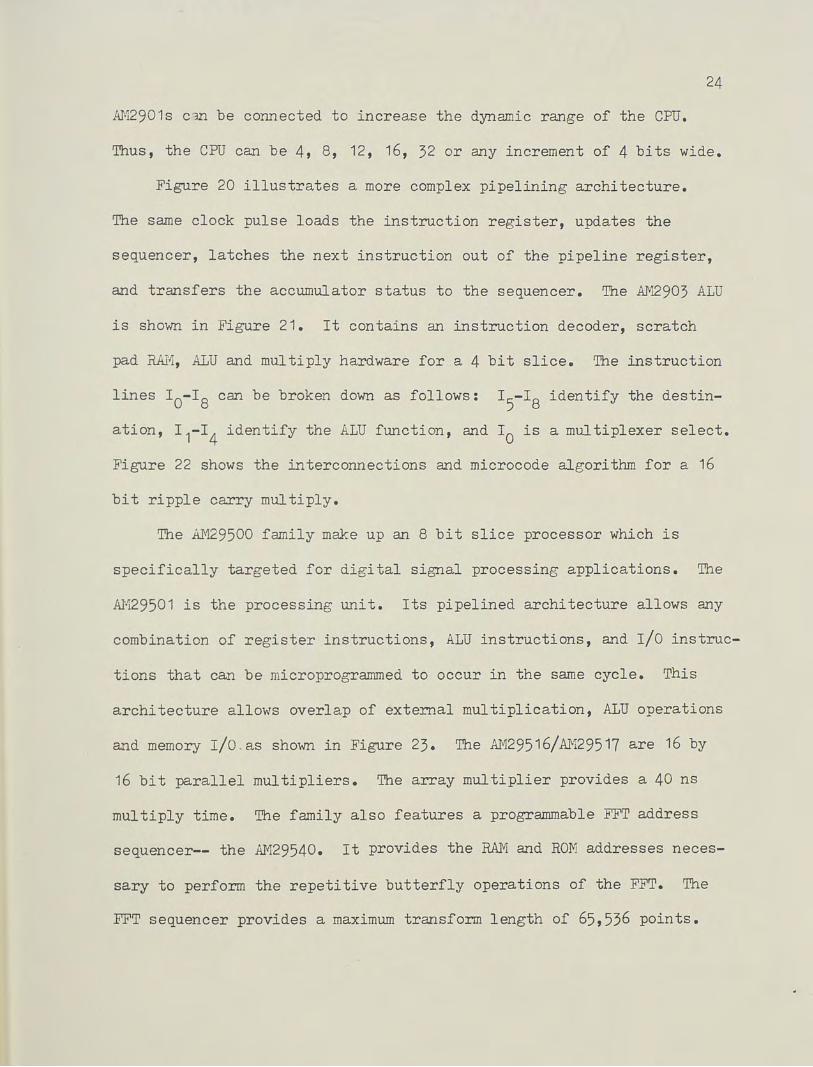
AM2901s c-m be connected to increase the dynamic range of the CPU.
Thus, the CPU can be 4, 8, 12, 16, 32 or any increment of 4 bits wide.
Figure 20 illustrates a more complex pipelining architecture.
The same clock pulse loads the instruction register, updates the
sequencer, latches the next instruction out of the pipeline register,
and transfers the accumulator status to the sequencer. The AM2903 ALU
is shown in Figure 21. It contains an instruction decoder, scratch
pad RAM, ALU and multiply hardware for a 4 bit slice. The instruction
lines r0-r8 can be broken down as follows: r 5-r8 identify the destin
ation, r 1-r4 identify the ALU function, and r0 is a multiplexer select.
Figure 22 shows the interconnections and microcode algorithm for a 16
bit ripple carry multiply.
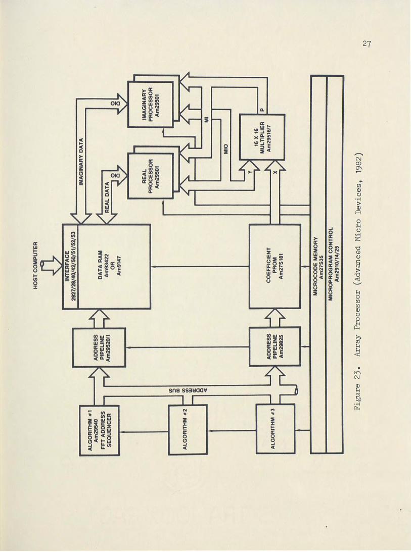
The AM29500 family make up an 8 bit slice processor which is
specifically targeted for digital signal processing applications. The
A1'129501 is the processing unit. Its pipelined architecture allows any
combination of register instructions, ALU instructions, and I/O instruc
tions that can be microprogrammed to occur in the same cycle. This
architecture allows overlap of external multiplication, ALU operations
and memory I/0 -as shown in Figure 23. The AM29516/AM29517 are 16 by
16 bit parallel multipliers. The array multiplier provides a 40 ns
multiply time. The family also features a programmable FFT address
sequencer-- the AM29540. It provides the RAM and ROM addresses neces
sary to perform the repetitive butterfly operations of the FFT. The
FFT sequencer provides a maximum transform length of 65,536 points.

BLOCK DIAGRAM
DATA IN
Ao - 3 e>------r--+--_. :DDRESS ADORES: t----.,,C---cJ llo - J
RAM MllTE iJl ENABLE
A B 1'--llO---DATA DUT DATADUT
~IN
~OVRCJ-------+---....;:i~
SI~ ~>l-------+-------1
l!IVe>-------+-------OtJ
iTN r>------
i:E D------4 INSTRUCTION e DECODE
CP
Vt>-------.....(~!5Gi
..----r---~c:ir 08o- J
0100
----ClCP
----a Vee
----ClGND
Figure 21. AH2903 Arithmetic Logic Unit (ALU) (Advanced Micro Devices, 1982)
25
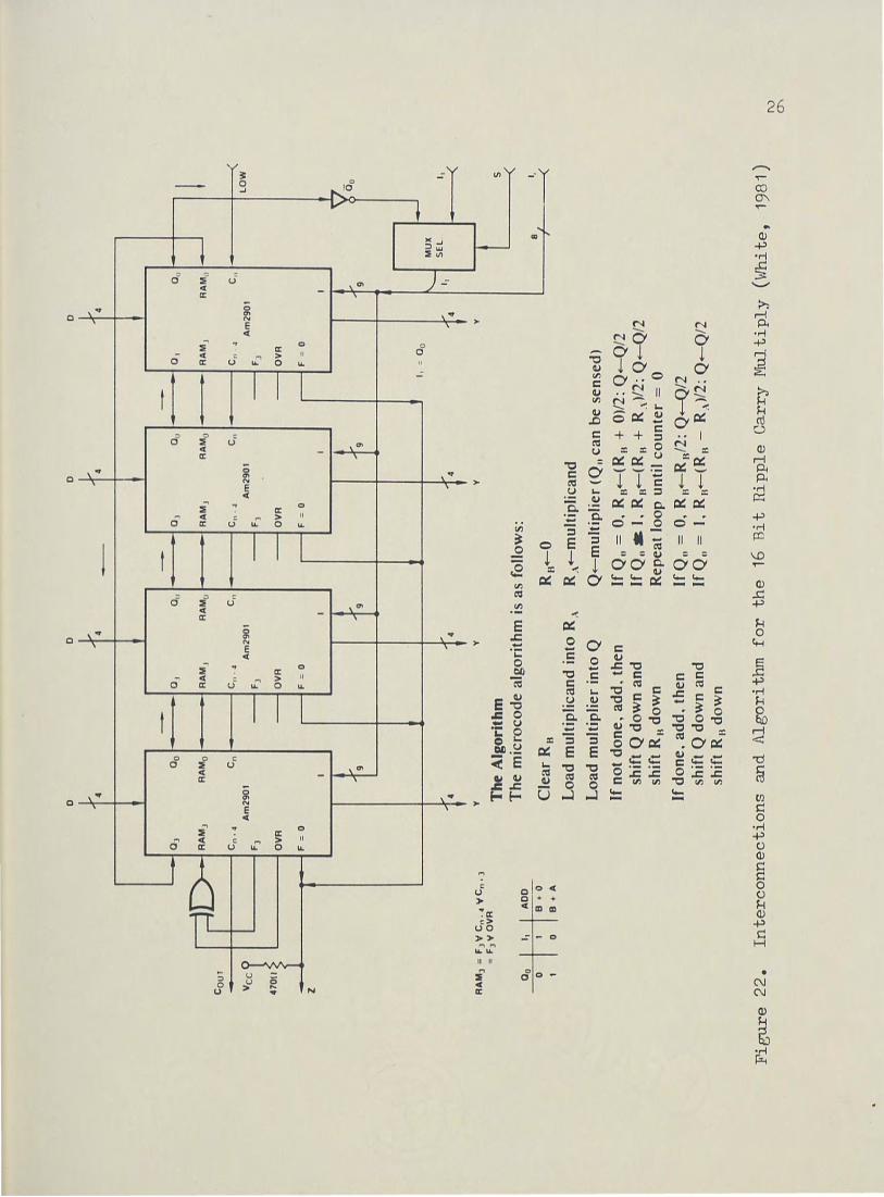
........
.._.
O:i
Cou
r r;
=)D
--A
AM
3
Cn
·4
Ve
e
F3
470!
1 >
.>
O
VA
F =
0 z R
AM
3 =
F:i V
C,,
. 4
V C
, 1,
3 =
F 3V
OV
A
Oo
I 1,
I A
DO
0
1 B
+ 0
0 0
D
D
Lo--
.; "
,.v
... v
... 4
4 -
4 4
I I l
---
-O
o -
Oi
Ou
OJ
Ou
a,
AA
M0
-A
AM
J A
A M
u R
AM
J R
AM
0 R
AM
J
Cn
c ...
4 c,
, c,
,. 4
c,,
c ...
4 A
m2
90
1
Am
29
01
A
m2
90
1
Am
29
01
-
F3
-F
J -
F3
-O
VA
-
OV
A
-O
VA
~
F =
0
-F
= 0
-F
= 0
I I
I
' I
,..v
[,..
...
i.-
9 ..
9 9
• I,
=
00
v ...
v ,..
.i.-
v ....
4 4
4 ..
4 '
v v
v v
The
Alg
orit
hm
Th
e m
icro
cod
e al
gori
thm
is
as f
ollo
ws:
r1~".lr
D
Lo
ad m
ulti
plic
and
into
R"
Lo
ad m
ulti
plie
r in
to Q
If n
ot
do
ne,
ad
d,
then
sh
ift
Q d
ow
n a
nd
sh
ift
R"
do
wn
If d
on
e. a
dd
, th
en
shif
t Q
do
wn
an
d
shif
t R
n d
ow
n
D
n
R "
+-m
ulti
plic
and
Q+
-mu
ltip
lier
(Q
., ca
n b
e se
nse
d)
If Q
0 =
0,
Rn+
-( R
u +
0)/
2: Q
+-Q
/2
If Q
11 &
I,
Rn+
-< R
n+
R.\)
/2:
Q+
-Q/2
R
epea
t lo
op u
ntil
co
un
ter
= 0
If Q
11 =
0,
Ru+
-R1/2
: Q
+-Q
/2
If Q
11 =
I ,
R n
+-( R
tt -
R .·\
)/2:
Q +
-Q/2
Ou
RA
M0
, __
l c .
. -
~ '
LO
W
I ,.v 9
6 O
o
I , __
[\..
_ M
UX
11
SE
L
'· " I
t s "
8/
I,
·--<
Fig
ure
2
2.
Inte
rco
nn
ecti
on
s an
d A
lgo
rith
m f
or
the
16 B
it R
ipp
le
Car
ry M
ult
iply
(W
hit
e,
1981
) I\
)
0\
ALG
OR
ITH
M #
1
Am
29
54
0
1 '
FF
T A
DD
RE
SS
S
EQ
UE
NC
ER
ALG
OR
ITH
M #
2
ALG
OR
ITH
M #
3
fl) ::>
m
fl)
fl) w
a:
Q
Q c
AD
DR
ES
S
PIP
ELI
NE
A
m29
520/
1
AD
DR
ES
S
PIP
ELI
NE
A
m2
98
25
HO
ST
CO
MP
UT
ER
INT
ER
FA
CE
2
92
7/2
8/4
0/4
2/5
0/5
1/5
2/5
3
DA
TA
RA
M
Am
93
42
2
OR
A
m91
47
CO
EF
FIC
IEN
T
PR
OM
A
m27
S18
1
MIC
RO
CO
DE
ME
MO
RY
A
m27
S35
MIC
RO
PR
OG
RA
M C
ON
TR
OL
Am
29
10
/14
/25
IMA
GIN
AR
Y D
AT
A
RE
AL
P
RO
CE
SS
OR
A
m29
501
MIO
16 x
16
IMA
GIN
AR
Y
PR
OC
ES
SO
R
Am
2950
1
Ml
MU
LTIP
LIE
R I p
I
Am
2951
6/7
Fig
ure
23.
A
rra
y
Pro
cess
or
(Adv
ance
d M
icro
Dev
ices
, 19
82)
I\)
-..J
28
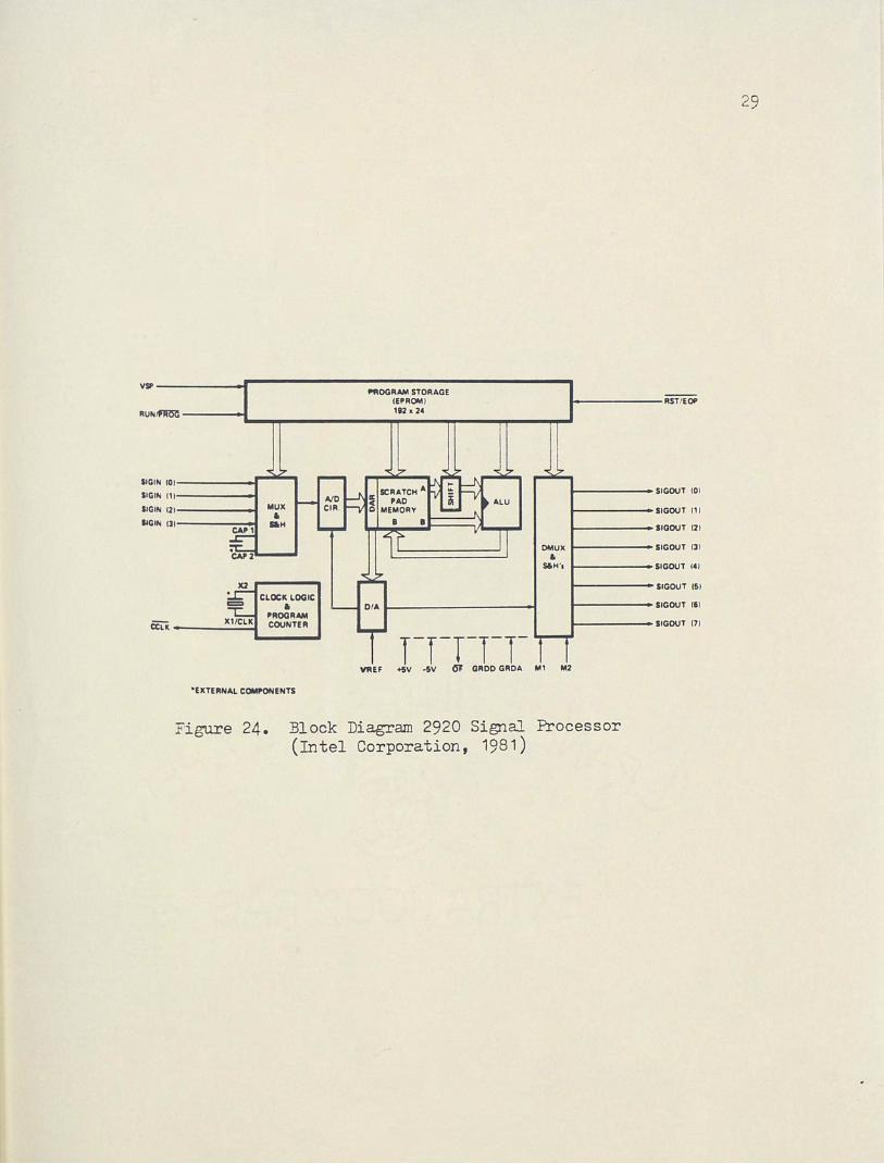
4. Single Chip Signal Processors
The Intel 2920 is a programmable single chip signal processor.
It contains an input multiplexer, a sample hold, an analog to digital
converter, a scratch pad RAM, an EPROM, an ALU, a digital to analog
converter and an output multiplexer on a single chip. The 2920 is
designed to replace analog subsystems such as filters, threshold
detectors, limiters, oscillators, and waveform generators to name a
few. The 2920 has a dynamic range limited to nine bi ts and a band
width limited to 13 KHz. Figure 24 shows a block diagram for the
processor.
The TMS320 is a single chip microcomputer aimed at giving both
the design ease of a general purpose microprocessor and the high
throughput of a rnultichip design. The TIVl.8320 is based on a modified
Harvard architecture which supports separate program and data memory
spaces. This architecture allows for the overlap of fetch and execute
cycles. The chip also features a 16 X 16 multiply at 200 ns and gives
a full 32 bit result. Figure 25 shows a TMS320 FIR filter implementa
tion and corresponding speed of execution.
v~~~~~~-1----------------------------------------.. '°"OGRAM STORAGE IEPROM l -------RST/EOP 192 • 2C RUN.flWC ____ .. .... ...,.,----------...., ...... ----.~--....,.~--..... ~
SIGIN 101------lr-.-.,..,
SIGIN 111-----_.
llGIN 121-----_.
llGIN 131-----_. CAP1
•CAP2
MUX
• aH
CLOCK LOGIC
• PROGRAM COUNTER
"EXTERNAL COMPONENTS
A/O CIR.
OMUX a.
S&H·a
DIA
Figure 24. Block Diagram 2920 Signal Processor (Intel Corporation, 1981)
SIGOUT 10)
SIGOUT 111
SIGOUT 121
SIGOUT Il l
SIGOUT !Cl
SIGOUT 151
SIGOUT 161
SIGOUT (71
29
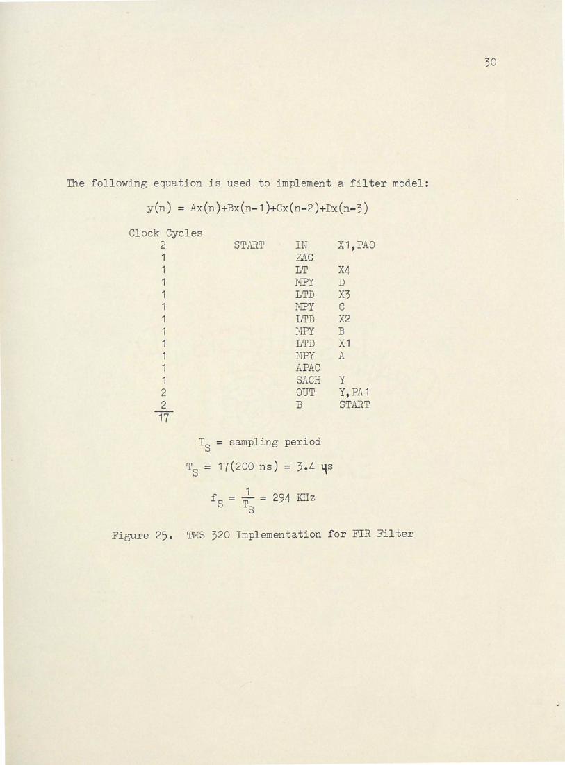
The following equation is used to implement a filter model:
y(n) = Ax(n)+Bx(n-1)+Cx(n-2)+Dx(n-3)
Clock Cycles 2 1 1 1 1 1 1 1 1 1 1 1 2 2
17
START IN ZAC LT MPY LTD MPY LTD MPY LTD :MPY APAC SACH OUT B
TS = sampling period
Ts = 17(200 ns) = 3.4 qs
f = -1 = 294 KHz
S TS
X1, PAO
X4 D X3 c X2 B X1 A
y Y, PA 1 START
Figure 25. TMS 320 Implementation for FIR Filter
30

31
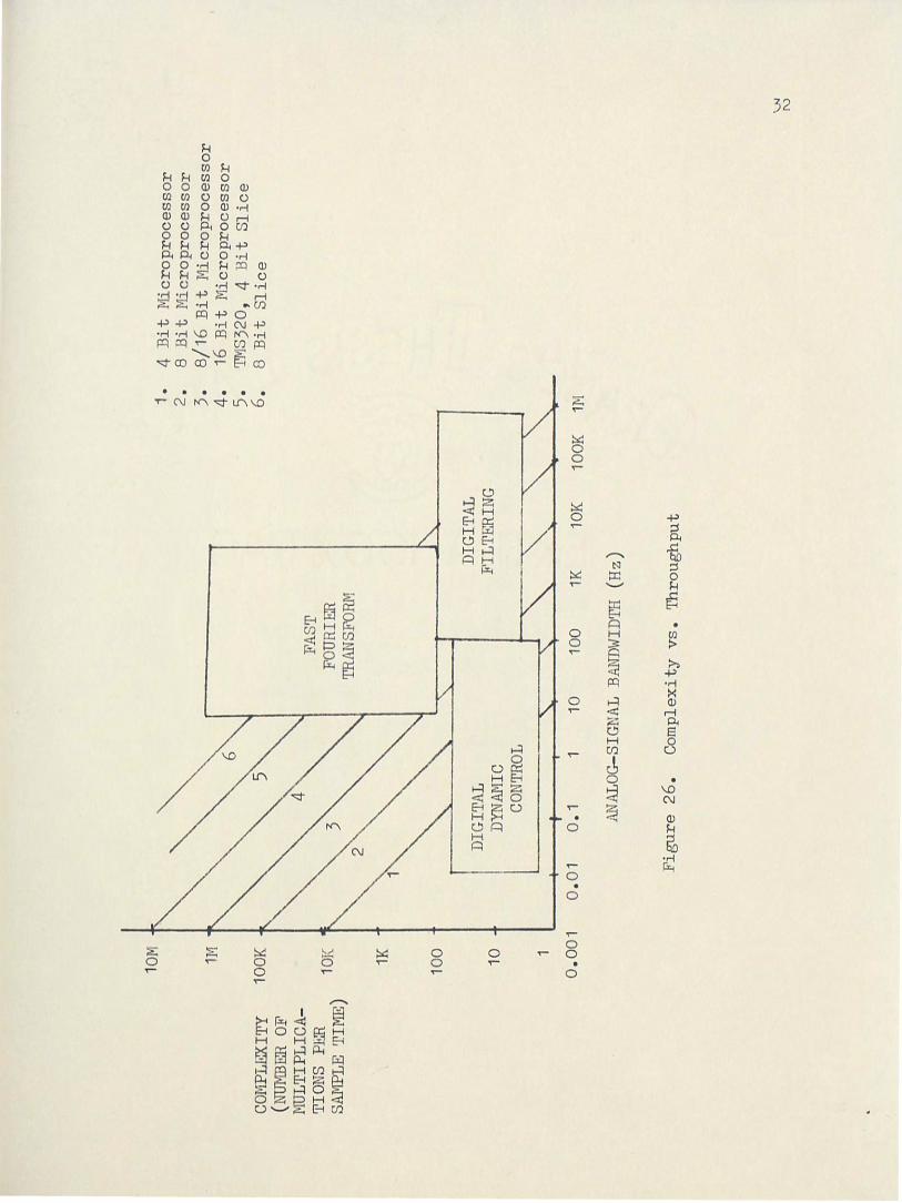
5. Comparison of Implementations
Figure 26 is a graph showing the complexity vs. throughput for
various implementations. The fast Fourier transform ranges from 32
point transform used in instrumentation to the very complex transforms
used in pattern recognition. The digital filtering applications range
from voice to video. The digital dynamic controllers require both
lower bandwidths and less complexity.
Figure 26 also shows the general techJ1ology requirements for
particular applications. For example, almost all control applications
can be handled without requiring a bit slice processor. Also very few
digital filtering applications can utilize an 8 bit microp~ocessor.
The TJV'S320 filter implementation of Figure 25 has a sampling
period of T8
equal to 294 KHz . Thus, if the input analog signal
requires at least 20 samples per period then the maximum bandwidth is
14.7 KHz.
BW = 1 20TS
Table 2 shows the design and cost tradeoffs for the various imple-
mentations. The 8 bit processor is the easiest to design and the
SSI/F1SI discrete logic is the most difficult. The TMS 320 provides an
excellent tradeoff of throughput and design time.
COM
PLEX
ITY
(N
UMBE
R OF
M
ULT
IPLI
CA
TI
ON
S PE
R
SAM
PLE
TIM
E)
10:M
1M
100K
10K
1K
100 10 1
0.0
01
0
.01
DIG
ITA
L DY
NAM
IC
CONT
ROL
0.1
1
10
FAST
FO
URI
ER
TRAN
SFOR
M
100
DIG
ITA
L FI
LTER
ING
1K
10K
.AN
ALO
G-S
IGN
AL
BAND
WID
TH
(Hz)
Fig
ure
2
6.
Co
mp
lex
ity
vs.
T
hro
ug
hp
ut
1.
2. 3.
4.
5.
6.
100K
lM
4 B
it ~
licroprocessor
8 B
it M
icro
pro
cess
or
8/1
6 B
it I
v'J.
icro
proc
esso
r 16
B
it M
icro
pro
cess
or
TM
S320
, 4
Bit
Sli
ce
8 B
it S
lice
\.>J
I'\.
)
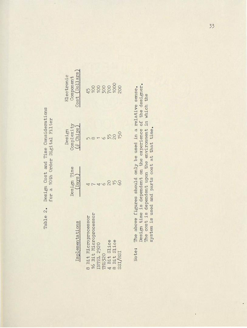
Tab
le 2
. D
esig
n
Co
st a
nd
Tim
e C
on
sid
erat
ion
s fo
r a
10
th O
rder
Dig
ital
Fil
ter
Des
ign
D
esig
n
Tim
e C
om
ple
xit
y
Imp
lem
enta
tio
ns
(Day
s)
(if
Ch
ips)
8 B
it M
icro
pro
cess
or
4 5
16 B
it M
icro
pro
cess
or
7 8
INT
EL
29
20
4 1
TN
S320
6
6 4
Bit
Sli
ce
20
35
8 B
it S
lice
15
20
SS
I/M
SI
60
150
Ele
ctr
on
ic
Com
pone
nt
Co
st
(Do
llars
)
45
100
100
300
700
1000
20
0
No
te:
The
ab
ov
e fi
gu
res
sho
uld
o
nly
be
use
d i
n
a re
lati
ve s
en
se.
Des
ign
ti
me
is
dep
end
ent
on
the
exp
erie
nce
o
f th
e d
esi
gn
er.
T
he
co
st i
s d
epen
den
t up
on
the
env
iro
nm
ent
in w
hich
th
e sy
stem
is u
sed
and
part
s co
st a
t th
at
tim
e.
"""'
"""'
X. CONCLUSION
Digital signal processing requires high speed arithmetic and con
trol sequencing capabilities for both digital filtering and spectral
analysis. The fundamental hardware elements are memories, adders, mul
tipliers and dividers. Memory can be classified as either static or
dynamic. It can also be classified by either writability or accessi
bility. ALUs can utilize the slower ripple carry adders or the more
complex lookahead carry adders. Division tends to be slower and more
complex than multiplication.
There is a range of possible solutions available to implement
digital signal processing applications. Correlation is a measure of
similarity between functions. The digital correlator may be used to
convolve two funGtions to realize a desired filter response. The gen
eral purpose microprocessors are desirable in applications requiring
limited dynamic range and limited bandwidth. The bit slice processor
can attain greater dynamic range and greater speed than the micropro
cessor-based system. It will usually, however, lead to a more complex
circuit design. The present trend is to develop single chip signal
processors to replace the more complex multichip bit slice designs.
REFERENCES
Advanced ~licro Devices. Array and Digital Sign.al Processing Products. Sunnyvale, CA: Advanced Ydcro Devices, 1982.
Cushman, Robert H. "Digitization Is on the Way for FFT Designs." Electronic Design News (August 1981): 99-106.
Eldon, John. Correlation-- A Powerful Technique for Digital Signal Processing. La Jolla, CA: TRW, 1981.
Gordon Ehud. "Speed AP Arithmetic Functions While Using Less Software." Electronics Design News (Nay 1982): 167-171.
Hill, Fredrick J., and Peterson, Gerald R. Digital Systems-- Hardware Organi zation and Design• New York: John Wiley, 1978.
Intel Corporation. Intel Component Data Catalog. Santa Clara, CA: Intel Corporation, 1981.
Nick, John R. "Understanding the .AM25LS2517 and AM25LS381." .AND Bipolar Mi croprocessor Logic and Interface Data Book. Sunnyvale, GA : Advanced I'-U.cro Devices, 1982.
1onolithic Memories Inc. :Monolithic Memories Bipolar LSI Databook. Sunnyvale, CA: Monolithic Memories Inc., 1981.
Eotorola Inc. Motorola Memory Data Manual. Austin, TX: Motorola Inc., 1980.
Rabiner, Lawrence R., and Gold, Bernard. Theory and Application of Digital Signal Processing. Englewood Cliffs, NJ: Prentice-Hall, 1975.
White, Donnamaie E. Bit Slice Design: Controllers and ALUs. New York: Garland STPl'fi Press, 1981.