The ATA Correlator - seti.org · The design goal of the ATA correlator is a 1024 channel, 100 MHz...
37
ATA memo 73 The ATA Correlator W.L. Urry, M. Wright, M. Dexter, D. MacMahon 16 Feb. 2007 Abstract This memo describes the current status of the ATA correlator. The correlator is designed for 352 antennas, dual polarization, with 1024 frequency channels over a 100 MHz bandwidth. The correlator uses an FX architecture with a polyphase filter which provides over 60 db rejection of RFI between frequency channels. The signal distribution from the antennas into the correlators uses a switched corner turner which converts the streams of data from the antennas with 1024 frequency channels into streams of data with all antennas for subsets of frequency channels. The correlator has a pipeline architecture which processes these subsets of frequency channels for all antennas, and uses inexpensive off-chip memory to reorder and integrate the data. The correlator is packaged in standard cPCI chassis and is being implemented in phases. Two prototype correlators each with 4 inputs (FX4) have been in use on the ATA telescope since May 2005. Two of the production correlator modules with 8 inputs each (FX8) were installed Jan 2007. The FX8 correlators use an ADC which directly samples the L-band analog IF system of the ATA telescope at 800 MHz, with a digital FIR filter to provide the 100 MHz input to the FX correlator. The next step is a 32-antenna dual polarization correlator (FX64) which requires eight FX8 modules and the addition of a corner turner to the cPCI backplane, followed by the correlator for 48 antennas dual polarization. The detailed design and implementation for up to 352 antennas is presented.
Transcript of The ATA Correlator - seti.org · The design goal of the ATA correlator is a 1024 channel, 100 MHz...
ATA memo 73
The ATA Correlator
W.L. Urry, M. Wright, M. Dexter, D. MacMahon
16 Feb. 2007
Abstract
This memo describes the current status of the ATA correlator. The correlator is designed for 352 antennas, dual polarization, with 1024 frequency channels over a 100 MHz bandwidth. The correlator uses an FX architecture with a polyphase filter which provides over 60 db rejection of RFI between frequency channels. The signal distribution from the antennas into the correlators uses a switched corner turner which converts the streams of data from the antennas with 1024 frequency channels into streams of data with all antennas for subsets of frequency channels. The correlator has a pipeline architecture which processes these subsets of frequency channels for all antennas, and uses inexpensive off-chip memory to reorder and integrate the data. The correlator is packaged in standard cPCI chassis and is being implemented in phases. Two prototype correlators each with 4 inputs (FX4) have been in use on the ATA telescope since May 2005. Two of the production correlator modules with 8 inputs each (FX8) were installed Jan 2007. The FX8 correlators use an ADC which directly samples the L-band analog IF system of the ATA telescope at 800 MHz, with a digital FIR filter to provide the 100 MHz input to the FX correlator. The next step is a 32-antenna dual polarization correlator (FX64) which requires eight FX8 modules and the addition of a corner turner to the cPCI backplane, followed by the correlator for 48 antennas dual polarization. The detailed design and implementation for up to 352 antennas is presented.

Correlator Design
The design goal of the ATA correlator is a 1024 channel, 100 MHz bandwidth, 352 antenna, dual polarization correlator. If there are sufficient funds we will build two 100 MHz bandwidth correlators that can be independently tuned to cover a total bandwidth of 200 MHz. The ATA correlator relies on an FX architecture which first divides the signal into frequency channels, usually by a Fourier transform, and then cross multiplies or correlates the result for each antenna pair. In order to avoid the severe channel to channel sidelobes produced by using the FFT as a filter bank, a polyphase technique is used[1] (figure 1). The severe problem of distributing the signals from the polyphase filter bank to the correlator is solved by using a corner turner of unique design[2](figure 4) which converts the 352 streams of 1024 channels into 342 streams of antennas of 3 frequency channels each. Normally, where the number of channels is evenly divided by the number of antennas, the number of streams leaving the corner turner will equal the number of streams entering. In our case, 3 channels times 352 is 1056. Since only 1024 channels are measured, 32 bogus channels are added and need not be correlated. The corner turner produces 352 data streams of 3 frequency channels each but 10 of these streams contain bogus data and need not be correlated. 342 data streams of 3 channels each will produce 1026 channels which is sufficient to carry all of the data with 2 channels to spare. In a non-square corner turner of this type, it is necessary to read out the 1056 channels in the time that it takes to generate the 1024 frequency channels in the filter bank card. It is necessary to run the corner turner and correlator cards at a slightly higher speed than the 100 MHz of the filter bank (figures 2&3). Each correlator is presented with a sequential stream of all of the antennas where all 61425 baselines are computed as the data enters one antenna at a time. A pipeline correlator was developed that minimizes the wiring required to expand a correlator to this size [3,4](figure 7). One innovation enables us to replace a significant amount expensive FPGA memory with less expensive off chip memory while preserving the basic idea of a pipeline correlator with low chip to chip wiring and easy expandability. This innovation requires the use of inexpensive memory as a signal buffer (figure 3) to reorder the frequency channel samples as they emerge from the polyphase filter bank. The large memory signal buffer also enables us to gain a great deal of flexibility in our implementation of the switched corner turner. The large memory signal buffer stores 1024 samples of each of the frequency bins. When the data enters the correlator, the 1024 samples are used to calculate and average several baselines. While these intermediate results are accumulated, the sums from the last set of baselines are accumulated into a large inexpensive memory rather than the expensive memory of the programmable gate array.

Implementation The system is housed in standard cPCI chassis and the boards are cPCI compatible. The cPCI standard is attractive because cPCI compatible components are widely available. A standard cPCI backplane has many unassigned pins that may be dedicated to the correlator. The cPCI standard also has specifications for cards that may be plugged into the back as well as the front of the chassis. The cards that accomplish the corner turn fit nicely into the back of the chassis while the polyphase filter bank cards and the correlator cards fit nicely into the front. The cPCI specification allows up to 8 cards in a backplane. We use a double backplane chassis that can accommodate a total of 16 cards. Each backplane is under the control of its own standard, off the shelf, computer card. Up to 6 of the card slots in each backplane are dedicated to polyphase filter bank cards for a total of 12 cards per chassis or they can be used for up to a total of 12 correlator cards per chassis. Each polyphase filter bank card has 8 filter banks filtering complex samples and can do the filtering for both polarizations of 4 antennas. A single filled cPCI chassis can do the filtering for up to 48 antennas with two polarizations. Similarly, one correlator card is required for every 4 antennas. Each correlator card is only partially loaded so that as more antennas must be accommodated, the depth of the pipeline is increased. A fully loaded correlator card can accommodate up to 352 antennas. A 48-antenna dual polarization correlator system consists of 2 cPCI chassis interconnected with 48 flat ribbon cables. A 352-antenna system will occupy 4 racks with 4 chassis each per tuning. The current power consumption estimate for the 352-antenna system is approximately 30 KW per tuning or 60 KW for the anticipated dual tuning system.
Data Acquisition Rates The smallest unit of integration is limited by the size of the data buffer that reorganizes the data before it is sent to the corner turner. The data buffer stores 1024 samples of each of the 1024 frequency samples. It requires 10 msec to fill this buffer. The correlation coefficients are calculated in 10 msec units. The dump time of the correlator is currently limited by the readout time of 6 slave 33 MHz 32 bit cPCI cards using a standard Linux operating system which reads out data in small bursts. This requires a high transaction overhead so that a full 352-antenna system would require a prohibitive amount of time to read out. The cPCI core that we are using is capable of transferring data as bus master so that close to the full bandwidth of the bus may be realized. The correlator design requires only 7 of the 8 cPCI card slots. As a future development, we plan to provide a data collection card in the extra slot that can be used to receive the data from the correlator cards at the full speed of the bus. With this improvement, we can dump a full 352-antenna, dual polarization, full Stokes correlator in approximately one second. A 48-antenna full Stokes correlator can be dumped in 150 msec. A 32-antenna system can be dumped in 70 msec. By averaging data in each of the cards we can dump a reduced resolution single polarization correlator in approximately 20 msec. By using 64 bit data transfers we can cut these times in half. The correlator is double

buffered so that integration need not be stopped while the data is read out.
Development Plan Two 4-antenna prototype correlators have been installed on the ATA telescope at Hat Creek since May 2005. They are being used for instrumental calibration and astronomy programs on the ATA. One of the prototype correlators was used on the PAPER array at the NRAO. The PAPER array is a prototype for a large N array to study the epoch of reionization [5]. The prototype has also been very useful in software development for wide field imaging [6]. At the present time we are just finishing an 8 input correlator using the production boards. The correlator consists of one 100 MHz bandwidth 8 input polyphase filter bank card and one 8 input correlator card. This system can handle 8 antennas with a single polarization, or 4 antennas dual polarization. The two card subsystem represents the smallest unit of our expandable system. Progress has been hampered by the fact that the ATA analog to digital, digital delay and fringe rotation system is still in development and it was necessary for us to build a digital front end to test the correlator system. The Radio Astronomy Lab has been working closely with the Berkeley Wireless Research Center (BWRC) to develop a computing platform for radio telescope DSP applications. We used 2 boards developed in collaboration with the group at BWRC. ADC and IBOB boards provide digital down conversion and FIR filters to match the 100 MHz bandwidth of the ATA correlator. With an inexpensive low pass filter to limit the bandwidth to 400 MHz, a sample rate of 800 MHz directly samples the L-band analog IF system of the ATA telescope which can be tuned anywhere within the 10 GHz bandwidth of the ATA telescope. The IBOB provides an additional digital output which is available to feed beamformers or packetized data into a computer cluster. Our added hardware has the advantage of making the correlator system much more portable, and provides direct calibration of the digital data into beamformers. Our next step is to expand the two card, 8 input subsystem into a 32-antenna dual polarization correlator. Advancing from an 8 input correlator to a 32-antenna correlator (64 input) measuring all 4 Stokes parameters requires the addition of a corner turner to the polyphase filter bank chassis backplane. This corner turner addition has been fully simulated and should work without much trouble. After the 32-antenna dual polarization correlator has been constructed it will be expanded to a 48-antenna dual polarization system. This step requires the addition of 4 polyphase filter bank cards, 4 correlator cards and 4 more corner turner cards and will require reprogramming the correlator and the corner turner cards. The electronics required to implement the non-square corner turner case will need to be built and tested. Almost all of the hardware required for the 48-antenna dual polarization system is in stock. The 48-antenna dual polarization system can also be used as a 96-antenna single polarization system so that as more antennas come on line they can be put directly to use.
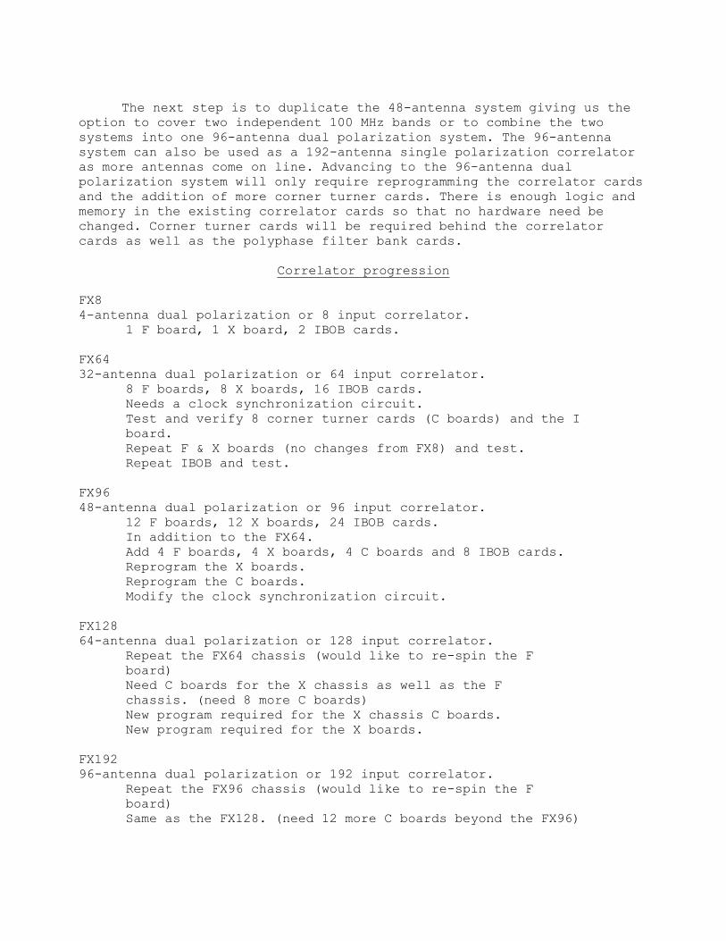
The next step is to duplicate the 48-antenna system giving us the option to cover two independent 100 MHz bands or to combine the two systems into one 96-antenna dual polarization system. The 96-antenna system can also be used as a 192-antenna single polarization correlator as more antennas come on line. Advancing to the 96-antenna dual polarization system will only require reprogramming the correlator cards and the addition of more corner turner cards. There is enough logic and memory in the existing correlator cards so that no hardware need be changed. Corner turner cards will be required behind the correlator cards as well as the polyphase filter bank cards.
Correlator progression FX8 4-antenna dual polarization or 8 input correlator. 1 F board, 1 X board, 2 IBOB cards. FX64 32-antenna dual polarization or 64 input correlator. 8 F boards, 8 X boards, 16 IBOB cards. Needs a clock synchronization circuit. Test and verify 8 corner turner cards (C boards) and the I board. Repeat F & X boards (no changes from FX8) and test. Repeat IBOB and test. FX96 48-antenna dual polarization or 96 input correlator. 12 F boards, 12 X boards, 24 IBOB cards. In addition to the FX64. Add 4 F boards, 4 X boards, 4 C boards and 8 IBOB cards. Reprogram the X boards. Reprogram the C boards. Modify the clock synchronization circuit. FX128 64-antenna dual polarization or 128 input correlator. Repeat the FX64 chassis (would like to re-spin the F board) Need C boards for the X chassis as well as the F chassis. (need 8 more C boards) New program required for the X chassis C boards. New program required for the X boards. FX192 96-antenna dual polarization or 192 input correlator. Repeat the FX96 chassis (would like to re-spin the F board) Same as the FX128. (need 12 more C boards beyond the FX96)

Conclusion The ATA correlator has an innovative design which solves several problems: A polyphase filter provides over 60 db isolation between frequency channels - essential in a high RFI environment. The correlator design solves the "large N" problem - the signal distribution from N antennas into N^2 correlators. A switched corner turner converts the N streams of data from the antennas with all the frequency channels into N streams of data with all antennas for subsets of frequency channels which are routed to N correlators. The correlators have an expandable pipeline architecture which processes the subsets of frequency channels for all antennas and uses inexpensive off-chip memory to reorder and integrate the data. Working with the Berkeley Wireless Research Center (BWRC), the polyphase filter and pipeline correlator designs have been incorporated into standard libraries which are used in the rapid development of FPGA and ASIC designs for other correlators which use standard FPGA platforms and Ethernet switches to route the signals. The switched corner turner described in this memo provides a low cost and low power solution which reduces the N^2 correlator inputs into N interconnections. The pipeline correlator is extendable and, with the corner turner, offers a low cost solution for telescopes with large numbers of antennas such as the ATA and SKA.
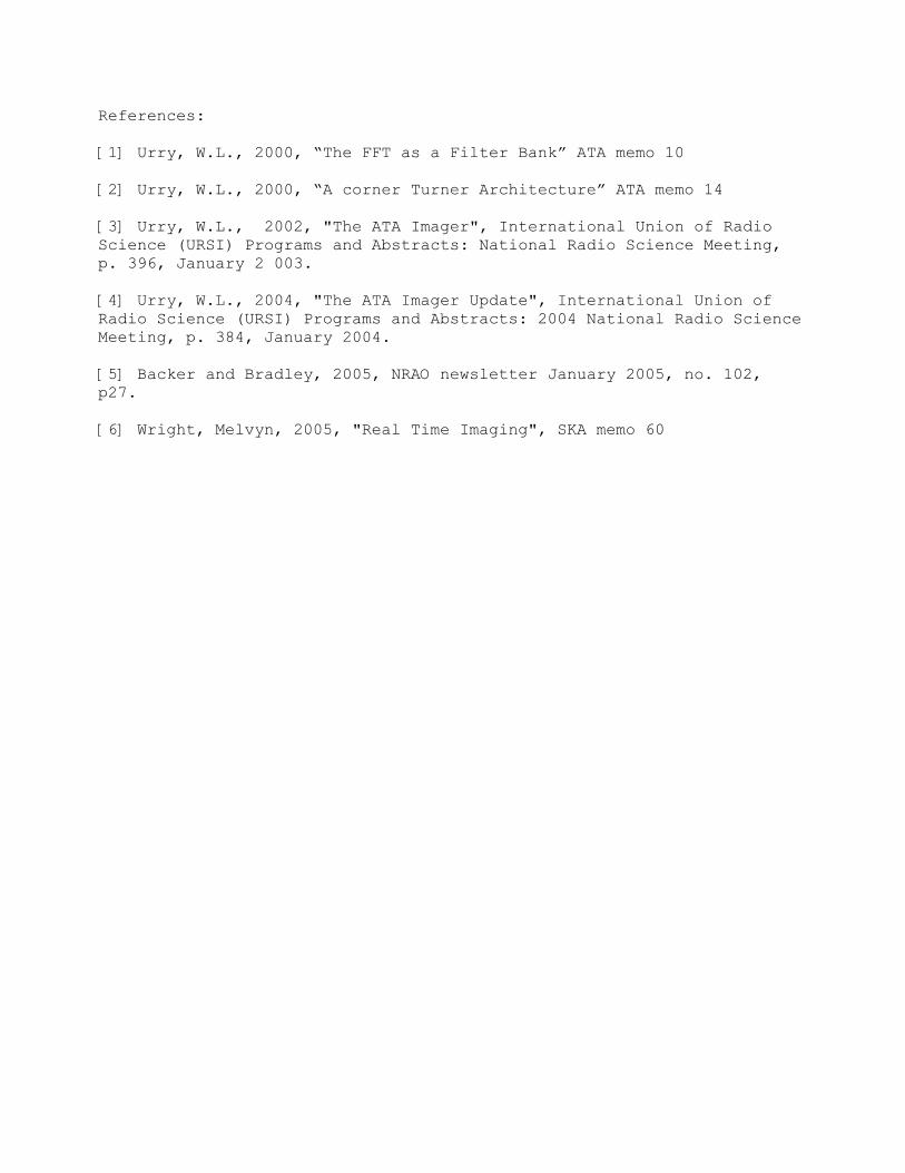
References: [1] Urry, W.L., 2000, “The FFT as a Filter Bank” ATA memo 10 [2] Urry, W.L., 2000, “A corner Turner Architecture” ATA memo 14 [3] Urry, W.L., 2002, "The ATA Imager", International Union of Radio Science (URSI) Programs and Abstracts: National Radio Science Meeting, p. 396, January 2 003. [4] Urry, W.L., 2004, "The ATA Imager Update", International Union of Radio Science (URSI) Programs and Abstracts: 2004 National Radio Science Meeting, p. 384, January 2004. [5] Backer and Bradley, 2005, NRAO newsletter January 2005, no. 102, p27. [6] Wright, Melvyn, 2005, "Real Time Imaging", SKA memo 60
Appendix
figure 1
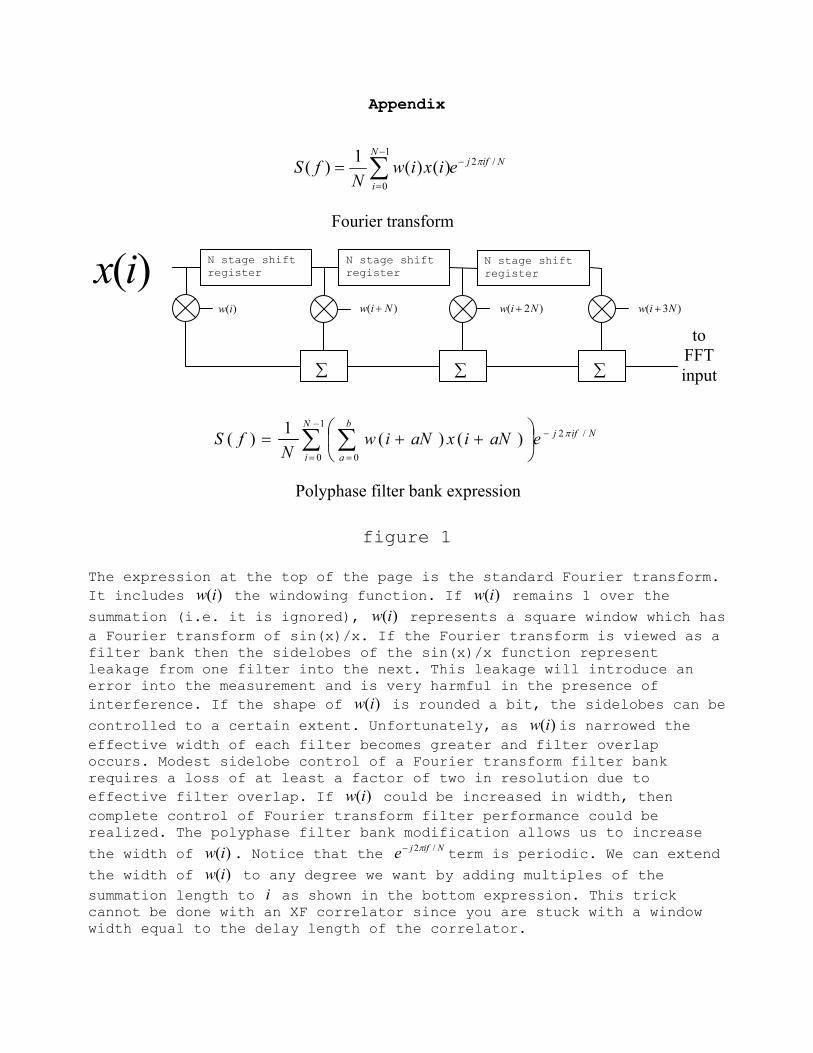
The expression at the top of the page is the standard Fourier transform. It includes )(iw the windowing function. If )(iw remains 1 over the
summation (i.e. it is ignored), )(iw represents a square window which has a Fourier transform of sin(x)/x. If the Fourier transform is viewed as a filter bank then the sidelobes of the sin(x)/x function represent leakage from one filter into the next. This leakage will introduce an error into the measurement and is very harmful in the presence of interference. If the shape of )(iw is rounded a bit, the sidelobes can be
controlled to a certain extent. Unfortunately, as )(iw is narrowed the effective width of each filter becomes greater and filter overlap occurs. Modest sidelobe control of a Fourier transform filter bank requires a loss of at least a factor of two in resolution due to effective filter overlap. If )(iw could be increased in width, then complete control of Fourier transform filter performance could be realized. The polyphase filter bank modification allows us to increase
the width of )(iw . Notice that the Nifje /2π− term is periodic. We can extend
the width of )(iw to any degree we want by adding multiples of the summation length to i as shown in the bottom expression. This trick cannot be done with an XF correlator since you are stuck with a window width equal to the delay length of the correlator.
)(ix
∑
N stage shift register
)( Niw +
NifjN
i
b
aeaNixaNiw
NfS /2
1
0 0)()(1)( π−
−
= =∑ ∑
++=
N stage shift register
)2( Niw +
to FFT input
N stage shift register
∑
)3( Niw +
∑
)(iw
Polyphase filter bank expression
NifjN
ieixiw
NfS /2
1
0)()(1)( π−
−
=∑=
Fourier transform
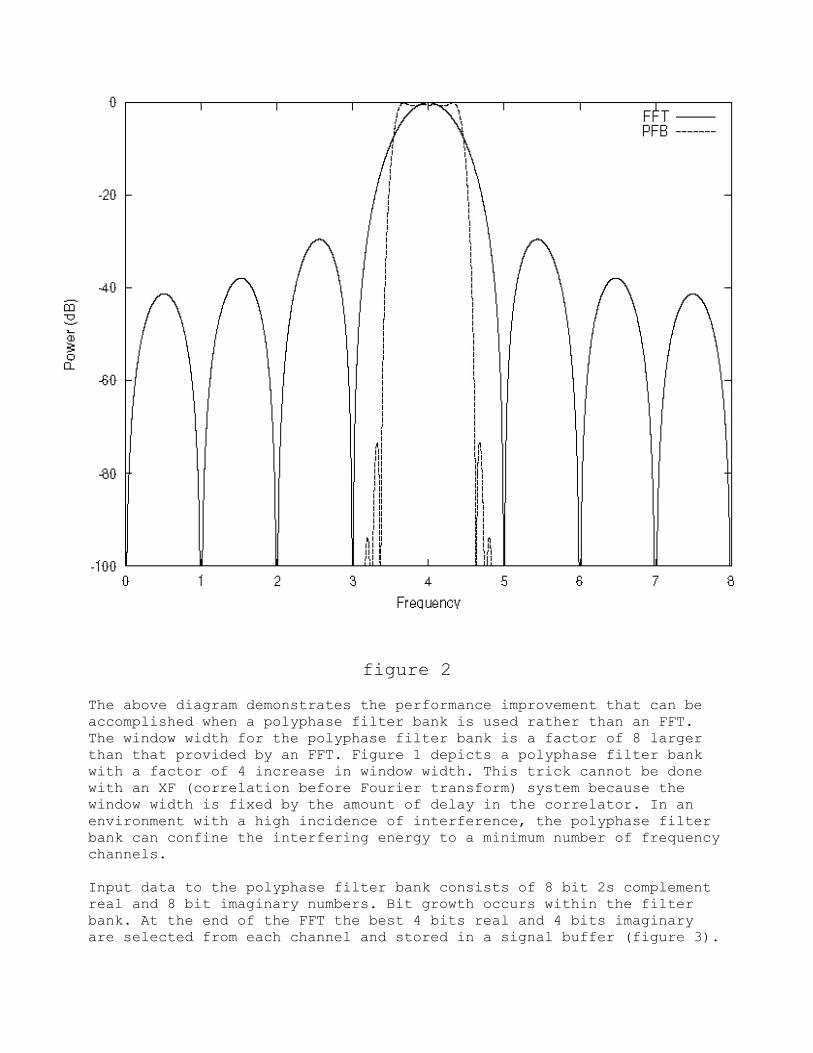
figure 2 The above diagram demonstrates the performance improvement that can be accomplished when a polyphase filter bank is used rather than an FFT. The window width for the polyphase filter bank is a factor of 8 larger than that provided by an FFT. Figure 1 depicts a polyphase filter bank with a factor of 4 increase in window width. This trick cannot be done with an XF (correlation before Fourier transform) system because the window width is fixed by the amount of delay in the correlator. In an environment with a high incidence of interference, the polyphase filter bank can confine the interfering energy to a minimum number of frequency channels. Input data to the polyphase filter bank consists of 8 bit 2s complement real and 8 bit imaginary numbers. Bit growth occurs within the filter bank. At the end of the FFT the best 4 bits real and 4 bits imaginary are selected from each channel and stored in a signal buffer (figure 3).
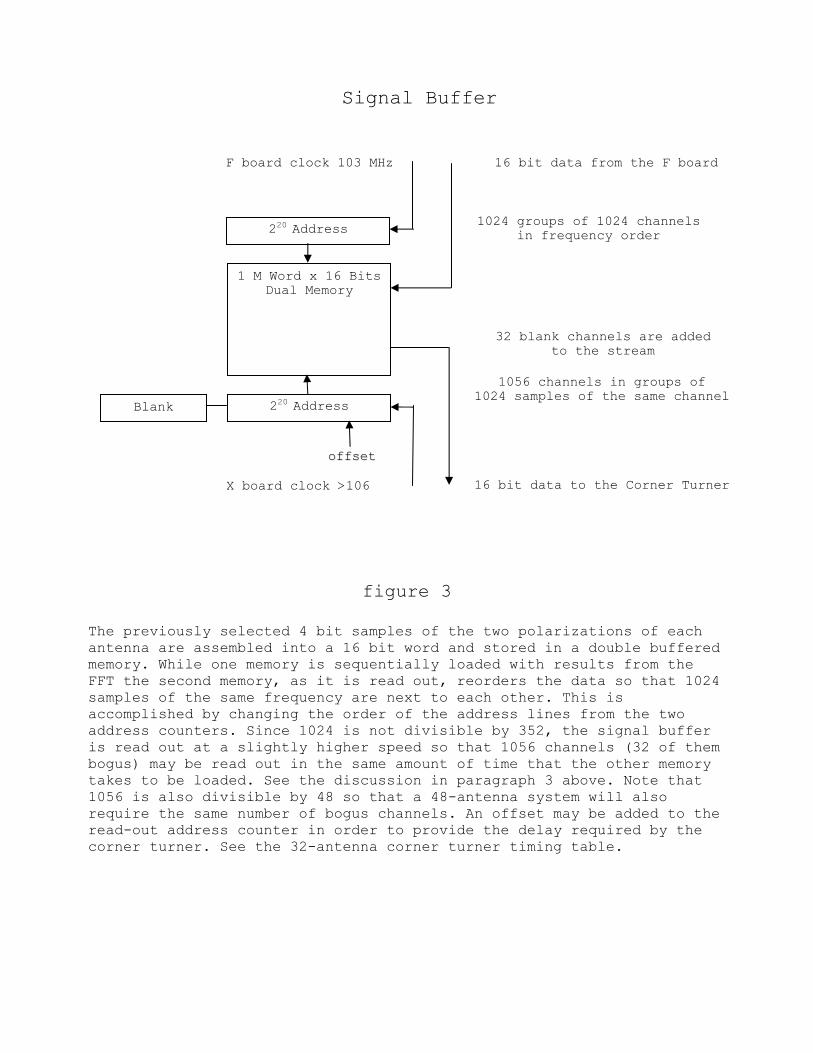
figure 3
The previously selected 4 bit samples of the two polarizations of each antenna are assembled into a 16 bit word and stored in a double buffered memory. While one memory is sequentially loaded with results from the FFT the second memory, as it is read out, reorders the data so that 1024 samples of the same frequency are next to each other. This is accomplished by changing the order of the address lines from the two address counters. Since 1024 is not divisible by 352, the signal buffer is read out at a slightly higher speed so that 1056 channels (32 of them bogus) may be read out in the same amount of time that the other memory takes to be loaded. See the discussion in paragraph 3 above. Note that 1056 is also divisible by 48 so that a 48-antenna system will also require the same number of bogus channels. An offset may be added to the read-out address counter in order to provide the delay required by the corner turner. See the 32-antenna corner turner timing table.
Signal Buffer
220 Address
1 M Word x 16 BitsDual Memory
220 Address
F board clock 103 MHz 16 bit data from the F board
Blank
X board clock >106 16 bit data to the Corner Turner
1024 groups of 1024 channelsin frequency order
1056 channels in groups of 1024 samples of the same channel
32 blank channels are added to the stream
ooffffsseett
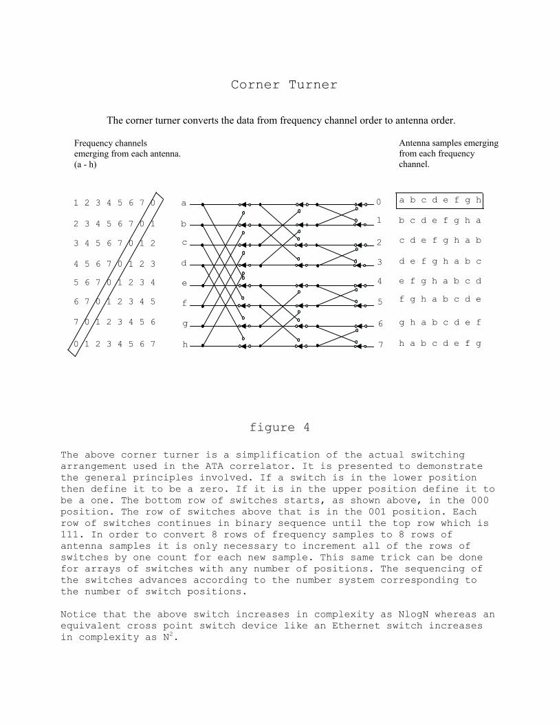
figure 4
The above corner turner is a simplification of the actual switching arrangement used in the ATA correlator. It is presented to demonstrate the general principles involved. If a switch is in the lower position then define it to be a zero. If it is in the upper position define it to be a one. The bottom row of switches starts, as shown above, in the 000 position. The row of switches above that is in the 001 position. Each row of switches continues in binary sequence until the top row which is 111. In order to convert 8 rows of frequency samples to 8 rows of antenna samples it is only necessary to increment all of the rows of switches by one count for each new sample. This same trick can be done for arrays of switches with any number of positions. The sequencing of the switches advances according to the number system corresponding to the number of switch positions. Notice that the above switch increases in complexity as NlogN whereas an equivalent cross point switch device like an Ethernet switch increases in complexity as N2.
The corner turner converts the data from frequency channel order to antenna order.
Frequency channels emerging from each antenna. (a - h)
Antenna samples emerging from each frequency channel.
Corner Turner
1 2 3 4 5 6 7 0
2 3 4 5 6 7 0 1
3 4 5 6 7 0 1 2
4 5 6 7 0 1 2 3
5 6 7 0 1 2 3 4
6 7 0 1 2 3 4 5
7 0 1 2 3 4 5 6
0 1 2 3 4 5 6 7
0
1
2
3
4
5
6
7
a
b
c
d
e
f
g
h
a b c d e f g h
b c d e f g h a
c d e f g h a b
d e f g h a b c
e f g h a b c d
f g h a b c d e
g h a b c d e f
h a b c d e f g
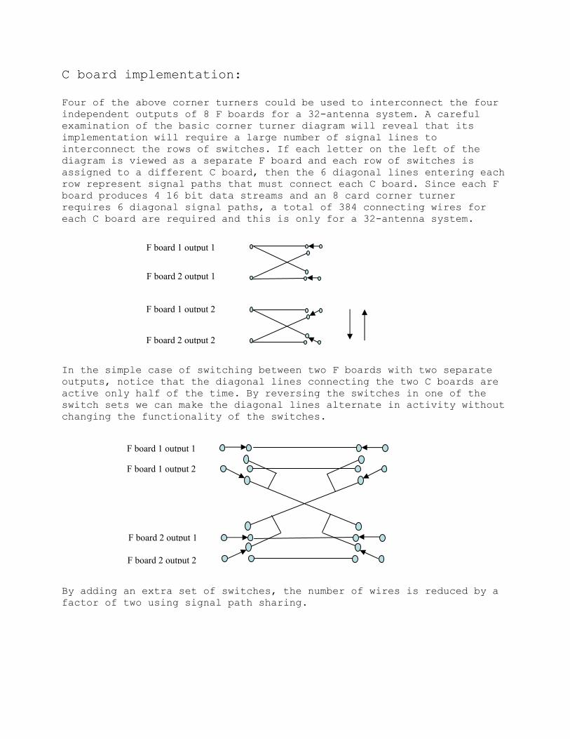
C board implementation: Four of the above corner turners could be used to interconnect the four independent outputs of 8 F boards for a 32-antenna system. A careful examination of the basic corner turner diagram will reveal that its implementation will require a large number of signal lines to interconnect the rows of switches. If each letter on the left of the diagram is viewed as a separate F board and each row of switches is assigned to a different C board, then the 6 diagonal lines entering each row represent signal paths that must connect each C board. Since each F board produces 4 16 bit data streams and an 8 card corner turner requires 6 diagonal signal paths, a total of 384 connecting wires for each C board are required and this is only for a 32-antenna system. In the simple case of switching between two F boards with two separate outputs, notice that the diagonal lines connecting the two C boards are active only half of the time. By reversing the switches in one of the switch sets we can make the diagonal lines alternate in activity without changing the functionality of the switches. By adding an extra set of switches, the number of wires is reduced by a factor of two using signal path sharing.
F board 1 output 1
F board 2 output 1
F board 1 output 2
F board 2 output 2
F board 1 output 1
F board 1 output 2
F board 2 output 1
F board 2 output 2
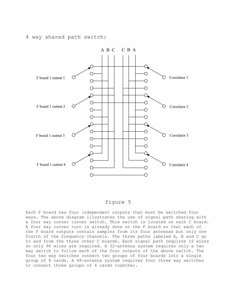
4 way shared path switch:
figure 5 Each F board has four independent outputs that must be switched four ways. The above diagram illustrates the use of signal path sharing with a four way corner turner switch. This switch is located on each C board. A four way corner turn is already done on the F board so that each of the F board outputs contain samples from its four antennas but only one fourth of the frequency channels. The three paths labeled A, B and C go to and from the three other C boards. Each signal path requires 16 wires so only 96 wires are required. A 32-antenna system requires only a two way switch to follow each of the four outputs of the above switch. The four two way switches connect two groups of four boards into a single group of 8 cards. A 48-antenna system requires four three way switches to connect three groups of 4 cards together.
A B C C B A
F board 1 output 1
F board 1 output 2
F board 1 output 3
F board 1 output 4 Correlator 4
Correlator 3
Correlator 2
Correlator 1
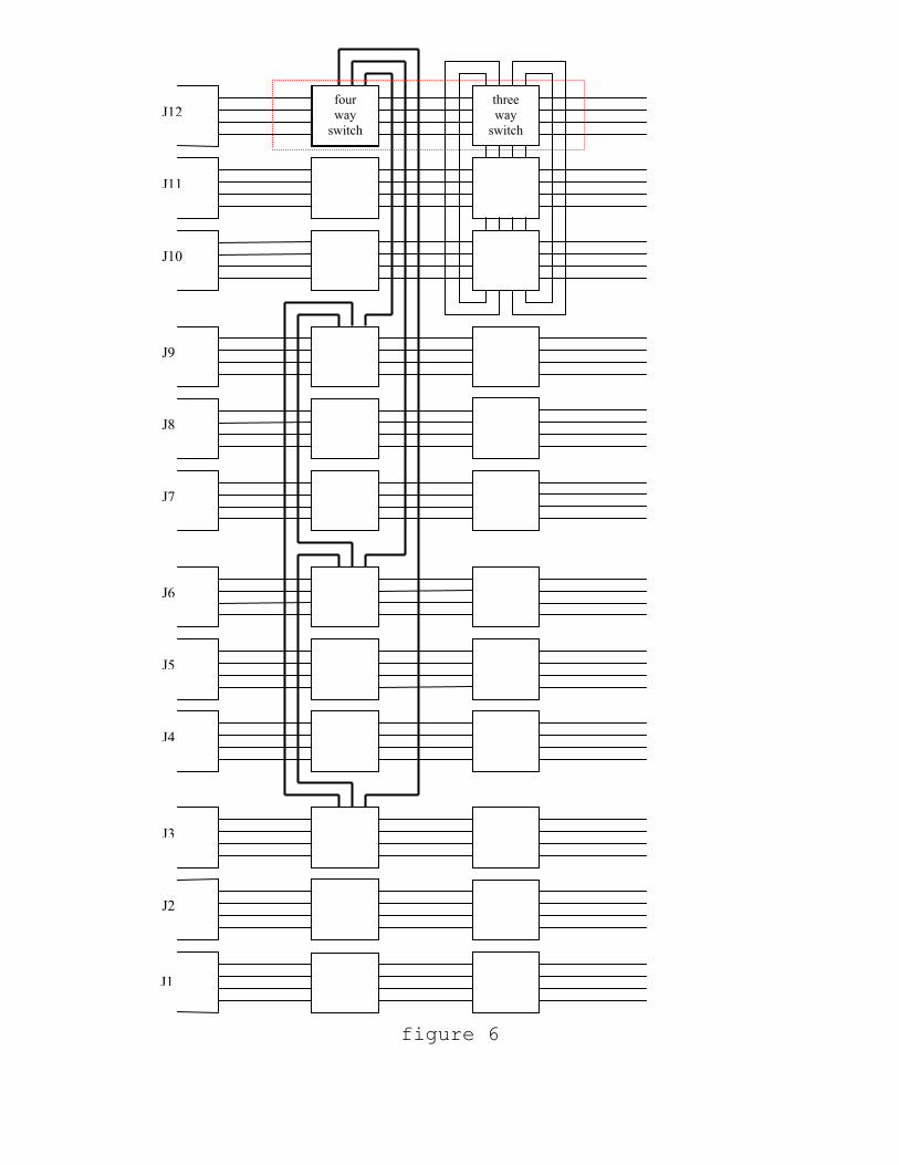
figure 6
J12
J2
J10
J9
J8
J7
J6
J5
J4
J3
J11
J1
four way
switch
three way
switch

I Board wiring: Figure 6 shows a subset of the I board wiring and its relationship to the corner turner switches. The J numbers on the left side of the diagram refer to card slots in the cPCI filter bank chassis. The lines extending to the right of the diagram represent cables going to the correlator chassis. One of the C boards is outlined in the red dashed line. A 12 board 48-antenna chassis is illustrated. All of the wiring is provided on the I board. Only a subset of the wiring is shown. Each of the 12 C boards requires a four way switch followed by a three way switch. A 32-antenna chassis requires a four way switch followed by a two way switch. The heavy lines represent the 32 wires of the A, B, and C lines. The lighter lines represent 16 wires each. The C boards are wired in nested star patterns. The four way switches are connected in a star with three other C boards. The three way switches are connected in a star with two other C boards. The four way switches require a total of 96 wires and the three way switches use 128 wires for a total of 224 wires to each C board.
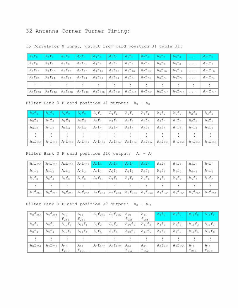
32-Antenna Corner Turner Timing: To Correlator 0 input, output from card position J1 cable J1: A0f0 A1f0 A2f0 A3f0 A4f0 A5f0 A6f0 A7f0 A8f0 A9f0 ... A31f0 A0f8 A1f8 A2f8 A3f8 A4f8 A5f8 A6f8 A7f8 A8f8 A9f8 ... A31f8 A0f16 A1f16 A2f16 A3f16 A4f16 A5f16 A6f16 A7f16 A8f16 A9f16 ... A31f16 A0f24 A1f24 A2f24 A3f24 A4f24 A5f24 A6f24 A7f24 A8f24 A9f24 ... A31f24
M M M M M M M M M M M M A0f248 A1f248 A2f248 A3f248 A4f248 A5f248 A6f248 A7f248 A8f248 A9f248 ... A31f248
Filter Bank 0 F card position J1 output: A0 – A3 A0f0 A1f0 A2f0 A3f0 A0f1 A1f1 A2f1 A3f1 A0f2 A1f2 A2f2 A3f2
A0f3 A1f3 A2f3 A3f3 A0f4 A1f4 A2f4 A3f4 A0f5 A1f5 A2f5 A3f5
A0f6 A1f6 A2f6 A3f6 A0f7 A1f7 A2f7 A3f7 A0f8 A1f8 A2f8 A3f8
M M M M M M M M M M M M A0f253 A1f253 A2f253 A3f253 A0f254 A1f254 A2f254 A3f254 A0f255 A1f255 A2f255 A3f255
Filter Bank 0 F card position J10 output: A4 – A7 A4f255 A5f255 A6f255 A7f255 A4f0 A5f0 A6f0 A7f0 A4f1 A5f1 A6f1 A7f1
A4f2 A5f2 A6f2 A7f2 A4f3 A5f3 A6f3 A7f3 A4f4 A5f4 A6f4 A7f4
A4f5 A5f5 A6f5 A7f5 A4f6 A5f6 A6f6 A7f6 A4f7 A5f7 A6f7 A7f7
M M M M M M M M M M M M A4f252 A5f252 A6f252 A7f252 A4f253 A5f253 A6f253 A7f253 A4f254 A5f254 A6f254 A7f254
Filter Bank 0 F card position J7 output: A8 – A11 A8f254 A9f254 A10
f254 A11 f254
A8f255 A9f255 A10 f255
A11 f255
A8f0 A9f0 A10f0 A11f0
A8f1 A9f1 A10f1 A11f1 A8f2 A9f2 A10f2 A11f2 A8f3 A9f3 A10f3 A11f3
A8f4 A9f4 A10f4 A11f4 A8f5 A9f5 A10f5 A11f5 A8f6 A9f6 A10f6 A11f6
M M M M M M M M M M M M A8f251 A9f251 A10
f251 A11 f251
A8f252 A9f252 A10 f252
A11 f252
A8f253 A9f253 A10 f253
A11 f253
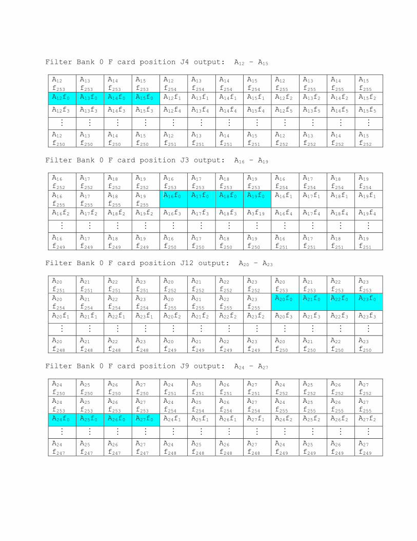
Filter Bank 0 F card position J4 output: A12 – A15 A12 f253
A13 f253
A14 f253
A15 f253
A12 f254
A13 f254
A14 f254
A15 f254
A12 f255
A13 f255
A14 f255
A15 f255
A12f0 A13f0 A14f0 A15f0 A12f1 A13f1 A14f1 A15f1 A12f2 A13f2 A14f2 A15f2
A12f3 A13f3 A14f3 A15f3 A12f4 A13f4 A14f4 A15f4 A12f5 A13f5 A14f5 A15f5
M M M M M M M M M M M M A12 f250
A13 f250
A14 f250
A15 f250
A12 f251
A13 f251
A14 f251
A15 f251
A12 f252
A13 f252
A14 f252
A15 f252
Filter Bank 0 F card position J3 output: A16 – A19 A16 f252
A17 f252
A18 f252
A19 f252
A16 f253
A17 f253
A18 f253
A19 f253
A16 f254
A17 f254
A18 f254
A19 f254
A16 f255
A17 f255
A18 f255
A19 f255
A16f0 A17f0 A18f0 A19f0 A16f1 A17f1 A18f1 A19f1
A16f2 A17f2 A18f2 A19f2 A16f3 A17f3 A18f3 A3f19 A16f4 A17f4 A18f4 A19f4
M M M M M M M M M M M M A16 f249
A17 f249
A18 f249
A19 f249
A16 f250
A17 f250
A18 f250
A19 f250
A16 f251
A17 f251
A18 f251
A19 f251
Filter Bank 0 F card position J12 output: A20 – A23 A20 f251
A21 f251
A22 f251
A23 f251
A20 f252
A21 f252
A22 f252
A23 f252
A20 f253
A21 f253
A22 f253
A23 f253
A20 f254
A21 f254
A22 f254
A23 f254
A20 f255
A21 f255
A22 f255
A23 f255
A20f0 A21f0 A22f0 A23f0
A20f1 A21f1 A22f1 A23f1 A20f2 A21f2 A22f2 A23f2 A20f3 A21f3 A22f3 A23f3
M M M M M M M M M M M M A20 f248
A21 f248
A22 f248
A23 f248
A20 f249
A21 f249
A22 f249
A23 f249
A20 f250
A21 f250
A22 f250
A23 f250
Filter Bank 0 F card position J9 output: A24 – A27 A24 f250
A25 f250
A26 f250
A27 f250
A24 f251
A25 f251
A26 f251
A27 f251
A24 f252
A25 f252
A26 f252
A27 f252
A24 f253
A25 f253
A26 f253
A27 f253
A24 f254
A25 f254
A26 f254
A27 f254
A24 f255
A25 f255
A26 f255
A27 f255
A24f0 A25f0 A26f0 A27f0 A24f1 A25f1 A26f1 A27f1 A24f2 A25f2 A26f2 A27f2
M M M M M M M M M M M M A24 f247
A25 f247
A26 f247
A27 f247
A24 f248
A25 f248
A26 f248
A27 f248
A24 f249
A25 f249
A26 f249
A27 f249
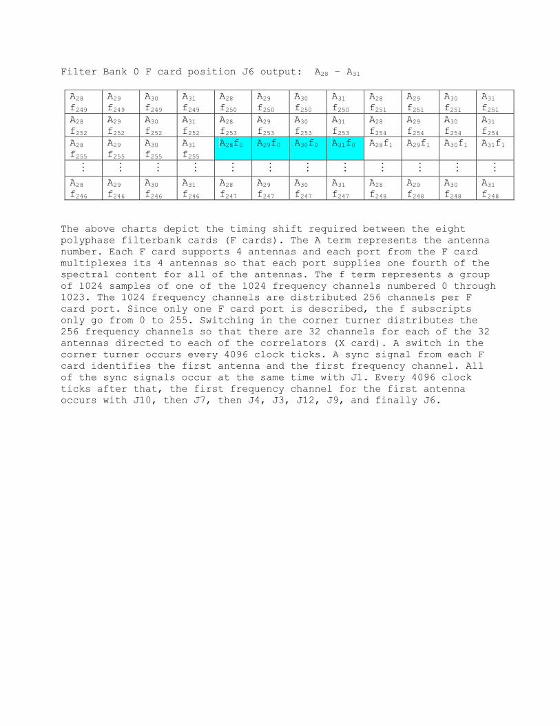
Filter Bank 0 F card position J6 output: A28 – A31 A28 f249
A29 f249
A30 f249
A31 f249
A28 f250
A29 f250
A30 f250
A31 f250
A28 f251
A29 f251
A30 f251
A31 f251
A28 f252
A29 f252
A30 f252
A31 f252
A28 f253
A29 f253
A30 f253
A31 f253
A28 f254
A29 f254
A30 f254
A31 f254
A28 f255
A29 f255
A30 f255
A31 f255
A28f0 A29f0 A30f0 A31f0 A28f1 A29f1 A30f1 A31f1
M M M M M M M M M M M M A28 f246
A29 f246
A30 f246
A31 f246
A28 f247
A29 f247
A30 f247
A31 f247
A28 f248
A29 f248
A30 f248
A31 f248
The above charts depict the timing shift required between the eight polyphase filterbank cards (F cards). The A term represents the antenna number. Each F card supports 4 antennas and each port from the F card multiplexes its 4 antennas so that each port supplies one fourth of the spectral content for all of the antennas. The f term represents a group of 1024 samples of one of the 1024 frequency channels numbered 0 through 1023. The 1024 frequency channels are distributed 256 channels per F card port. Since only one F card port is described, the f subscripts only go from 0 to 255. Switching in the corner turner distributes the 256 frequency channels so that there are 32 channels for each of the 32 antennas directed to each of the correlators (X card). A switch in the corner turner occurs every 4096 clock ticks. A sync signal from each F card identifies the first antenna and the first frequency channel. All of the sync signals occur at the same time with J1. Every 4096 clock ticks after that, the first frequency channel for the first antenna occurs with J10, then J7, then J4, J3, J12, J9, and finally J6.
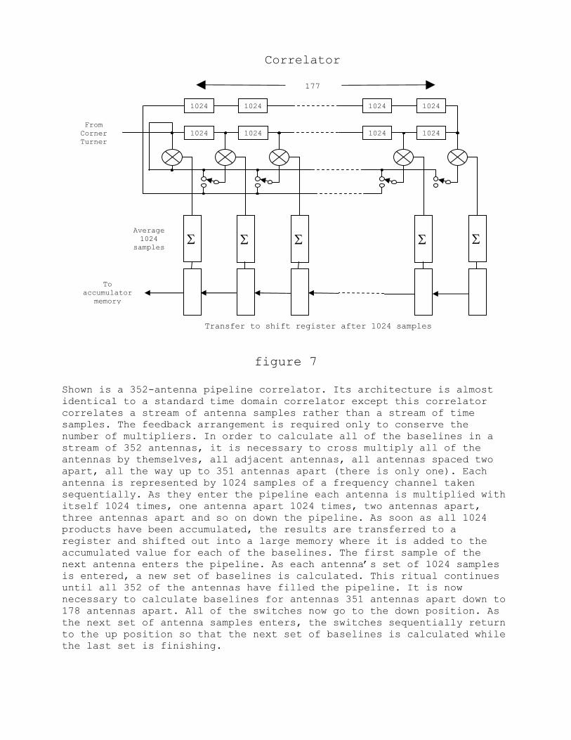
figure 7
Shown is a 352-antenna pipeline correlator. Its architecture is almost identical to a standard time domain correlator except this correlator correlates a stream of antenna samples rather than a stream of time samples. The feedback arrangement is required only to conserve the number of multipliers. In order to calculate all of the baselines in a stream of 352 antennas, it is necessary to cross multiply all of the antennas by themselves, all adjacent antennas, all antennas spaced two apart, all the way up to 351 antennas apart (there is only one). Each antenna is represented by 1024 samples of a frequency channel taken sequentially. As they enter the pipeline each antenna is multiplied with itself 1024 times, one antenna apart 1024 times, two antennas apart, three antennas apart and so on down the pipeline. As soon as all 1024 products have been accumulated, the results are transferred to a register and shifted out into a large memory where it is added to the accumulated value for each of the baselines. The first sample of the next antenna enters the pipeline. As each antenna’s set of 1024 samples is entered, a new set of baselines is calculated. This ritual continues until all 352 of the antennas have filled the pipeline. It is now necessary to calculate baselines for antennas 351 antennas apart down to 178 antennas apart. All of the switches now go to the down position. As the next set of antenna samples enters, the switches sequentially return to the up position so that the next set of baselines is calculated while the last set is finishing.
1024 1024
1024 1024
1024 1024
1024 1024
Σ Σ Σ Σ ΣAverage 1024
samples
To accumulator
memory
Transfer to shift register after 1024 samples
From Corner Turner
Correlator
177
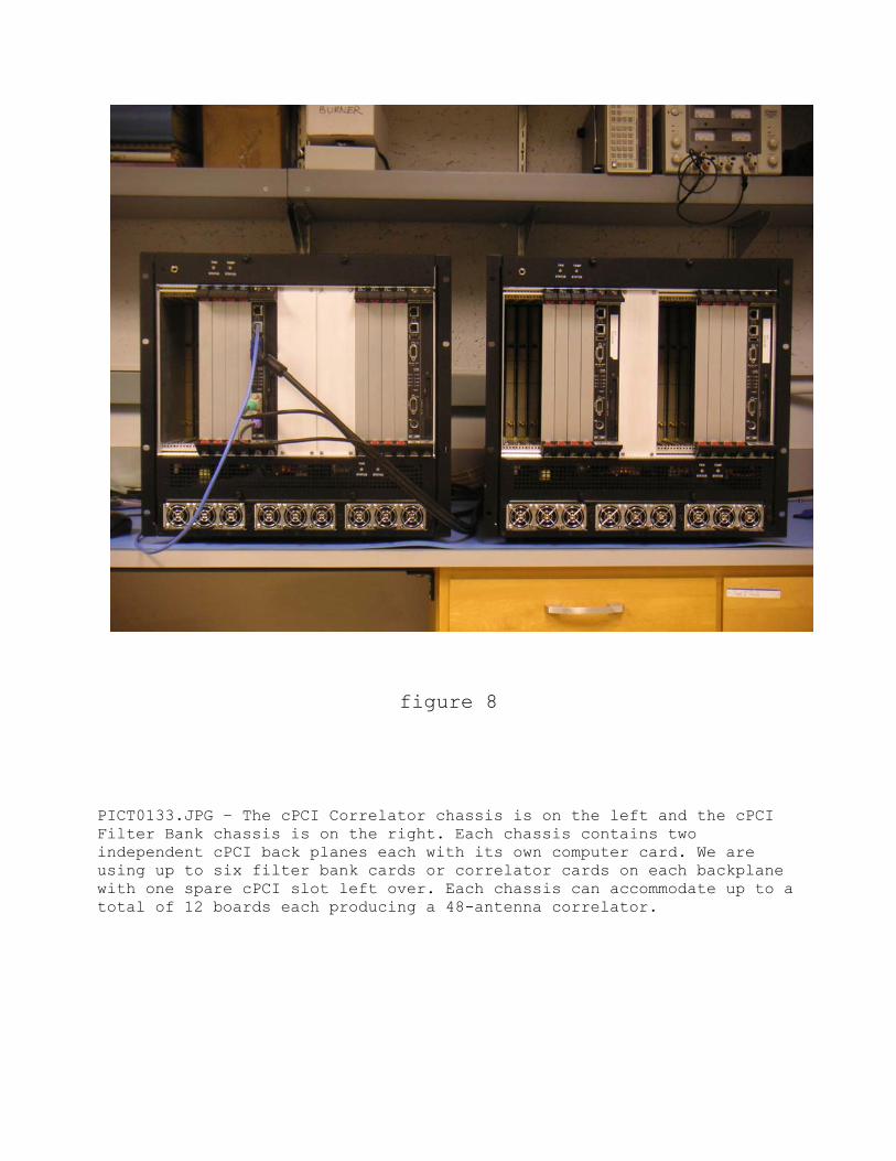
figure 8
PICT0133.JPG – The cPCI Correlator chassis is on the left and the cPCI Filter Bank chassis is on the right. Each chassis contains two independent cPCI back planes each with its own computer card. We are using up to six filter bank cards or correlator cards on each backplane with one spare cPCI slot left over. Each chassis can accommodate up to a total of 12 boards each producing a 48-antenna correlator.

figure 9 PICT0126.JPG – F Board. A single XC2VP50-6FF1152C Xilinx chip provides eight 1024 channel polyphase filter banks for four antennas with two polarizations each. The polyphase filter banks may be preceded by half band filters to reduce the input bandwidth in factor of 2 steps for narrower bandwidth observations. Each card has four signal buffers and a four way corner turner and produces four data streams of 256 frequency channels of the four antennas.
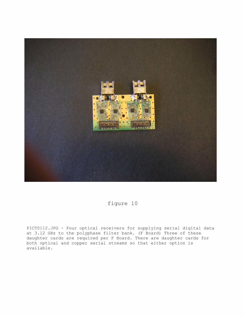
figure 10 PICT0112.JPG – Four optical receivers for supplying serial digital data at 3.12 GHz to the polyphase filter bank. (F Board) Three of these daughter cards are required per F Board. There are daughter cards for both optical and copper serial streams so that either option is available.
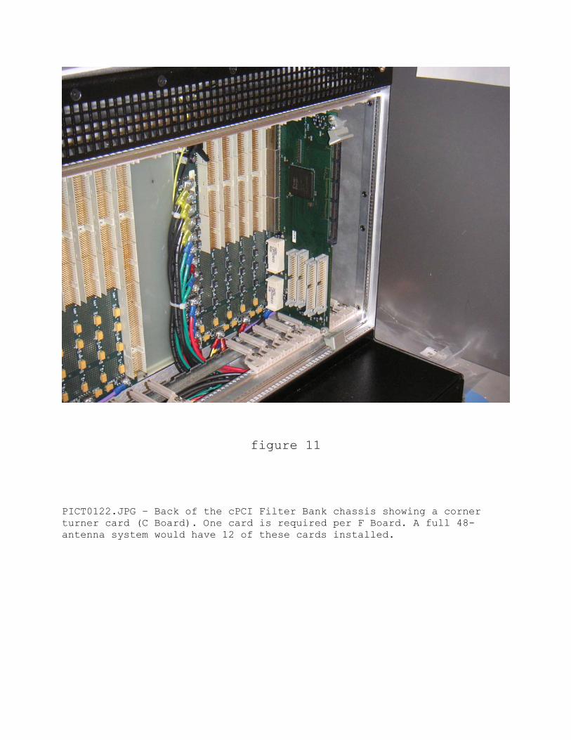
figure 11 PICT0122.JPG – Back of the cPCI Filter Bank chassis showing a corner turner card (C Board). One card is required per F Board. A full 48-antenna system would have 12 of these cards installed.
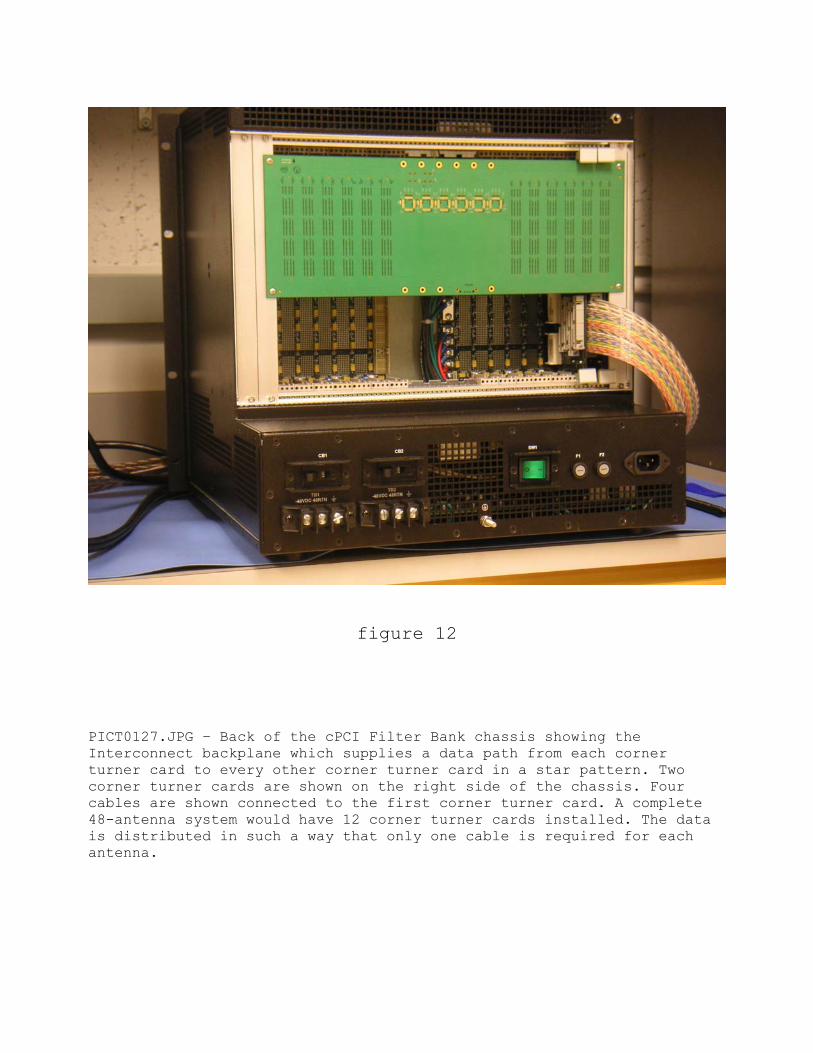
figure 12 PICT0127.JPG – Back of the cPCI Filter Bank chassis showing the Interconnect backplane which supplies a data path from each corner turner card to every other corner turner card in a star pattern. Two corner turner cards are shown on the right side of the chassis. Four cables are shown connected to the first corner turner card. A complete 48-antenna system would have 12 corner turner cards installed. The data is distributed in such a way that only one cable is required for each antenna.
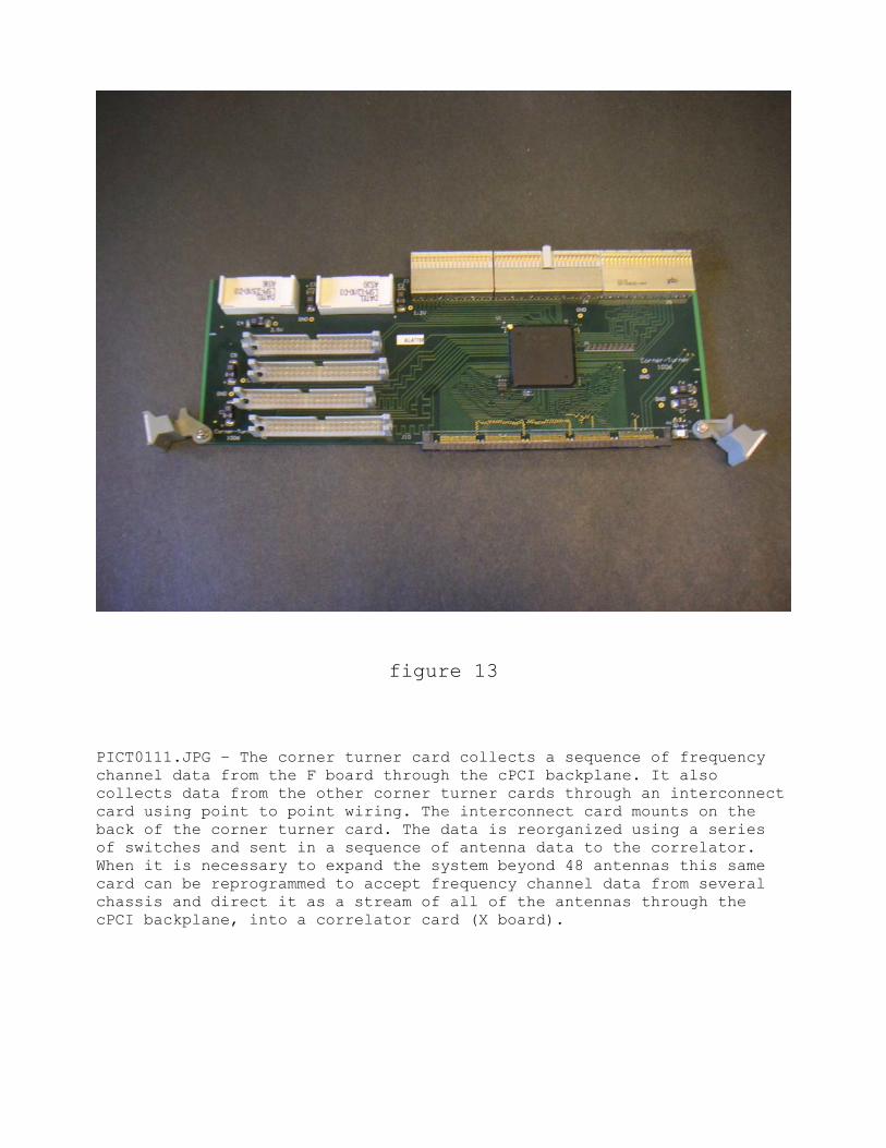
figure 13 PICT0111.JPG – The corner turner card collects a sequence of frequency channel data from the F board through the cPCI backplane. It also collects data from the other corner turner cards through an interconnect card using point to point wiring. The interconnect card mounts on the back of the corner turner card. The data is reorganized using a series of switches and sent in a sequence of antenna data to the correlator. When it is necessary to expand the system beyond 48 antennas this same card can be reprogrammed to accept frequency channel data from several chassis and direct it as a stream of all of the antennas through the cPCI backplane, into a correlator card (X board).
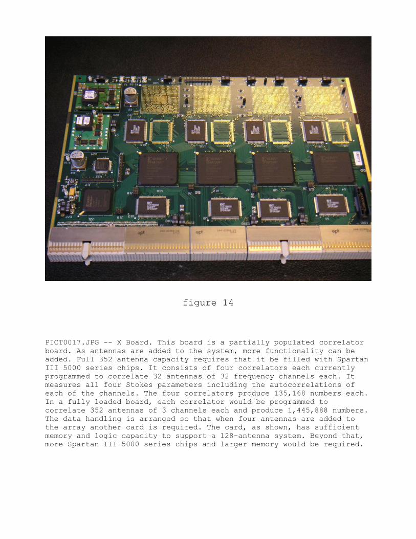
figure 14 PICT0017.JPG -- X Board. This board is a partially populated correlator board. As antennas are added to the system, more functionality can be added. Full 352 antenna capacity requires that it be filled with Spartan III 5000 series chips. It consists of four correlators each currently programmed to correlate 32 antennas of 32 frequency channels each. It measures all four Stokes parameters including the autocorrelations of each of the channels. The four correlators produce 135,168 numbers each. In a fully loaded board, each correlator would be programmed to correlate 352 antennas of 3 channels each and produce 1,445,888 numbers. The data handling is arranged so that when four antennas are added to the array another card is required. The card, as shown, has sufficient memory and logic capacity to support a 128-antenna system. Beyond that, more Spartan III 5000 series chips and larger memory would be required.
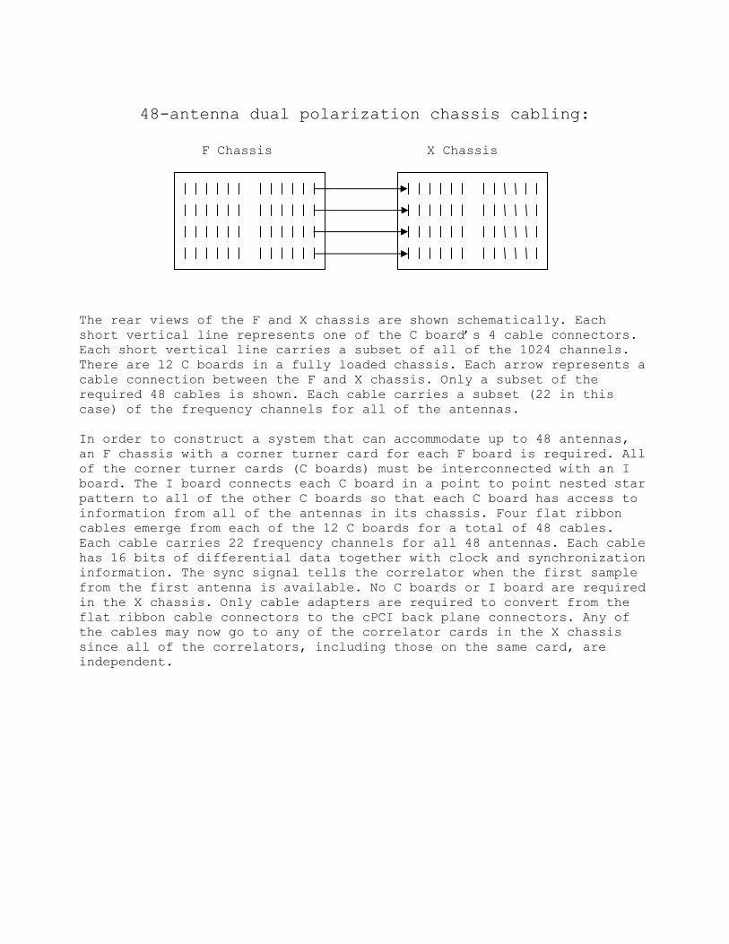
48-antenna dual polarization chassis cabling:
The rear views of the F and X chassis are shown schematically. Each short vertical line represents one of the C board’s 4 cable connectors. Each short vertical line carries a subset of all of the 1024 channels. There are 12 C boards in a fully loaded chassis. Each arrow represents a cable connection between the F and X chassis. Only a subset of the required 48 cables is shown. Each cable carries a subset (22 in this case) of the frequency channels for all of the antennas. In order to construct a system that can accommodate up to 48 antennas, an F chassis with a corner turner card for each F board is required. All of the corner turner cards (C boards) must be interconnected with an I board. The I board connects each C board in a point to point nested star pattern to all of the other C boards so that each C board has access to information from all of the antennas in its chassis. Four flat ribbon cables emerge from each of the 12 C boards for a total of 48 cables. Each cable carries 22 frequency channels for all 48 antennas. Each cable has 16 bits of differential data together with clock and synchronization information. The sync signal tells the correlator when the first sample from the first antenna is available. No C boards or I board are required in the X chassis. Only cable adapters are required to convert from the flat ribbon cable connectors to the cPCI back plane connectors. Any of the cables may now go to any of the correlator cards in the X chassis since all of the correlators, including those on the same card, are independent.
X ChassisF Chassis
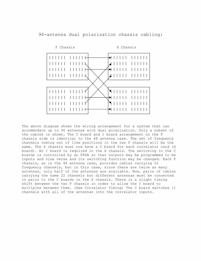
96-antenna dual polarization chassis cabling:
The above diagram shows the wiring arrangement for a system that can accommodate up to 96 antennas with dual polarization. Only a subset of the cables is shown. The C board and I board arrangement on the F chassis side is identical to the 48 antenna case. The set of frequency channels coming out of like positions in the two F chassis will be the same. The X chassis must now have a C board for each correlator card (X board). No I board is required in the X chassis. The switching in the C boards is controlled by an FPGA so that outputs may be programmed to be inputs and vise versa and its switching function may be changed. Each F chassis, as in the 48 antenna case, provides cables carrying 22 frequency channels, but in this case, since there are twice as many antennas, only half of the antennas are available. Now, pairs of cables carrying the same 22 channels but different antennas must be connected in pairs to the C boards in the X chassis. There is a slight timing shift between the two F chassis in order to allow the C board to multiplex between them. (See Correlator Timing) The C board switches 11 channels with all of the antennas into the correlator inputs.
F Chassis X Chassis
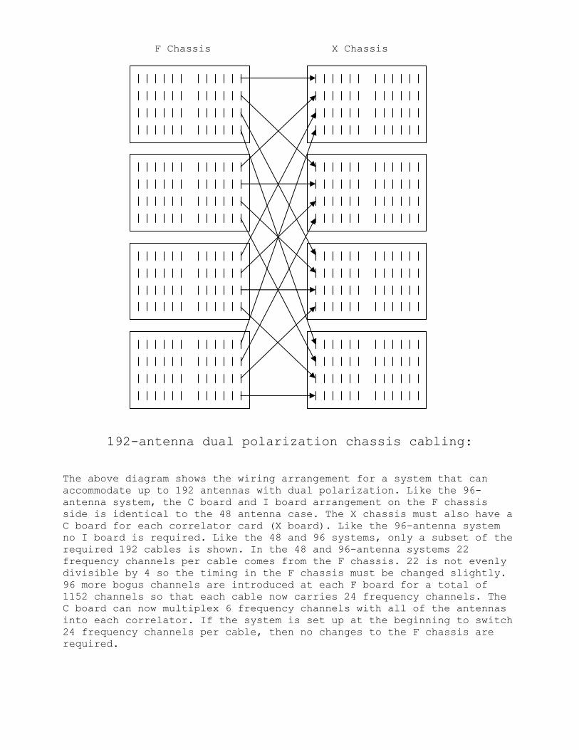
192-antenna dual polarization chassis cabling: The above diagram shows the wiring arrangement for a system that can accommodate up to 192 antennas with dual polarization. Like the 96-antenna system, the C board and I board arrangement on the F chassis side is identical to the 48 antenna case. The X chassis must also have a C board for each correlator card (X board). Like the 96-antenna system no I board is required. Like the 48 and 96 systems, only a subset of the required 192 cables is shown. In the 48 and 96-antenna systems 22 frequency channels per cable comes from the F chassis. 22 is not evenly divisible by 4 so the timing in the F chassis must be changed slightly. 96 more bogus channels are introduced at each F board for a total of 1152 channels so that each cable now carries 24 frequency channels. The C board can now multiplex 6 frequency channels with all of the antennas into each correlator. If the system is set up at the beginning to switch 24 frequency channels per cable, then no changes to the F chassis are required.
F Chassis X Chassis
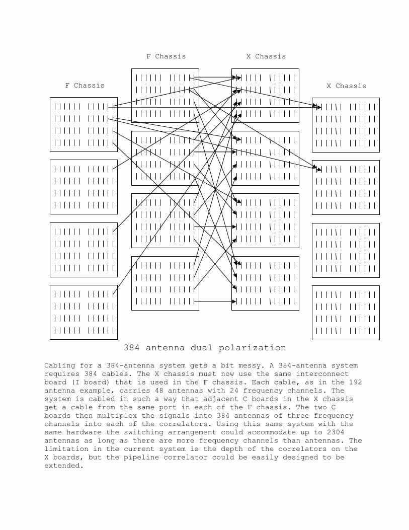
384 antenna dual polarization Cabling for a 384-antenna system gets a bit messy. A 384-antenna system requires 384 cables. The X chassis must now use the same interconnect board (I board) that is used in the F chassis. Each cable, as in the 192 antenna example, carries 48 antennas with 24 frequency channels. The system is cabled in such a way that adjacent C boards in the X chassis get a cable from the same port in each of the F chassis. The two C boards then multiplex the signals into 384 antennas of three frequency channels into each of the correlators. Using this same system with the same hardware the switching arrangement could accommodate up to 2304 antennas as long as there are more frequency channels than antennas. The limitation in the current system is the depth of the correlators on the X boards, but the pipeline correlator could be easily designed to be extended.
F Chassis X Chassis
F Chassis X Chassis
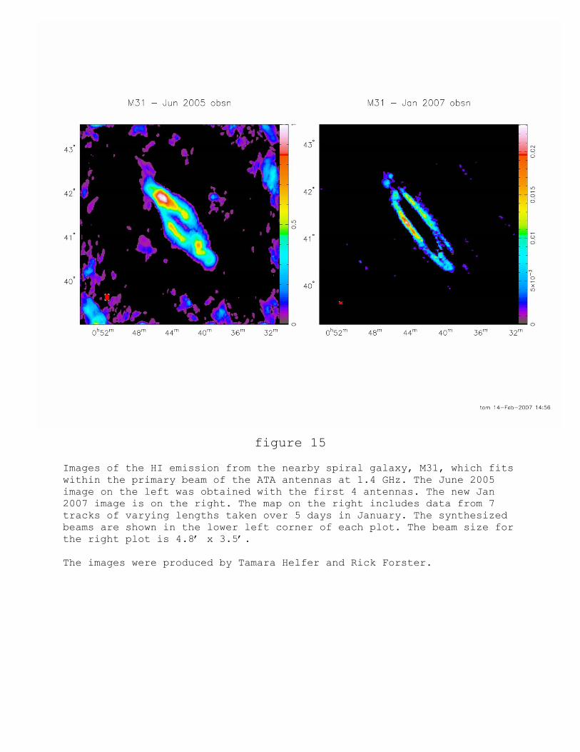
figure 15 Images of the HI emission from the nearby spiral galaxy, M31, which fits within the primary beam of the ATA antennas at 1.4 GHz. The June 2005 image on the left was obtained with the first 4 antennas. The new Jan 2007 image is on the right. The map on the right includes data from 7 tracks of varying lengths taken over 5 days in January. The synthesized beams are shown in the lower left corner of each plot. The beam size for the right plot is 4.8’ x 3.5’. The images were produced by Tamara Helfer and Rick Forster.
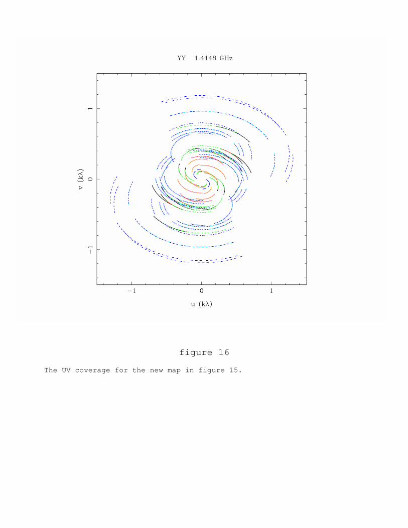
figure 16
The UV coverage for the new map in figure 15.
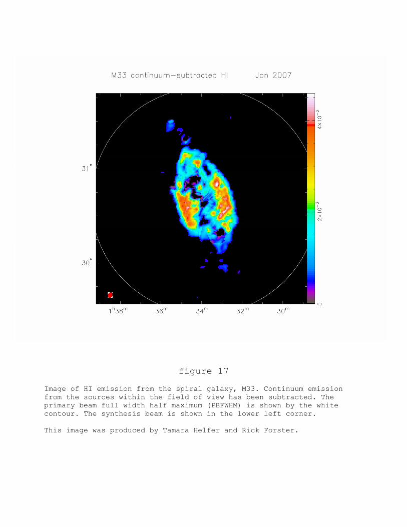
figure 17
Image of HI emission from the spiral galaxy, M33. Continuum emission from the sources within the field of view has been subtracted. The primary beam full width half maximum (PBFWHM) is shown by the white contour. The synthesis beam is shown in the lower left corner. This image was produced by Tamara Helfer and Rick Forster.

addendum:
The Ethernet switch option: It has been suggested that the filter bank part of the correlator could be connected to the correlator part by using industry standard serial links and commercial Ethernet switches. Indeed, the signal buffer in the F board could be used to collect the signal data into convenient packets. Xilinx produces FPGA chips with serializer-deserializer logic included. It seems that it would not take much added logic to add header information to each of these packets so that they could be steered to the proper locations. Unfortunately it requires more in system resources simply to accommodate an Ethernet switch than it does to directly install a corner turner switch. It is interesting to consider what would be required to convert the present system into one that can use Ethernet switches. The easiest thing to do would be to redesign the boards that are currently being used to accomodate the corner turner (C boards). It would be necessary to replace the relatively inexpensive Spartan III device with a more expensive Vertix Pro device that contains the logic required for at least 4 Ethernet serializer-deserializers. In order to avoid latency problems it would be required to add at least 2 large memory chips to act as signal buffers for the X board. The inexpensive 3M ribbon connectors would have to be replaced with expensive wide bandwidth Infiniband connectors. The cost of the C boards has increased by just adding the hardware necessary to plug into an Ethernet switch. We do save the cost of the passive board that interconnects the C boards. Now it is necessary, for a 352-antenna system, to buy a 704 port single direction Ethernet switch and 704 wide bandwidth cables. The problems presented by an Ethernet switch are not insurmountable, but they do represent design problems. To suggest that the signal distribution problem in an FX correlator may be solved simply by using an Ethernet switch rather than sitting down and working out the paths required in a corner turner is to ignore the engineering required to hook up an Ethernet switch. Simply install the Ethernet switch and the device will automatically determine the proper signal routing. The use of an Ethernet switch seems like a simple solution to a complex problem. An Ethernet switch, however, is not designed to solve the problems presented by a correlator. An Ethernet switch is designed to collect packets arriving at random times and direct them to the proper location in a competitive manner. If a collision occurs, then the loosing packet enters a queue and waits until the port is available. The result is variable latency and there is the very real danger that the packets will arrive from their different locations out of order. If the packets from the polyphase filterbanks entering the Ethernet switch are not reordered then all of the polyphase filter banks will produce the same set of frequency channel samples at the same time. These packets will all be sent to the same correlator at the same time. A collision is guaranteed. In fact, all of the correlators will suffer from the same problem. If

the Ethernet switch does not have enough storage in its queue, then it will lose data. The system will experience a massive denial of service. The collision problem can be reduced if the packets are scheduled in the same manner as the data in the corner turner. The corner turner is designed to function without collisions and it does this by controlling when the data is sent to the correlator and by using predetermined paths that guarantee no collisions will take place. An Ethernet switch must still select a suitable path through its network using its own internal logic. When an Ethernet switch starts up, it broadcasts messages to all of its ports in order to fill its address table. At the correlator end of the machine a serializer is needed to respond to the Ethernet switch as it establishes this table. We also need a deserializer feeding another signal buffer that can sort the data as it comes in as well as smooth out any latency problems. It must use the information in the header to organize the data according to antenna, frequency channel and time of arrival. Each correlator card must then assemble the data into the proper order before it can enter the correlator. The complexity involved in this problem and the amount of logic required to implement it is beginning to look very close if not more than the engineering complexity and amount of logic required to implement a corner turner. As an added complication, a commercial Ethernet switch is expected to have only 50% port utilization. This application will use close to 100% port utilization. In other words, a correlator application for an Ethernet switch will experience a factor of two increase in data throughput over what the manufacturer expects. There could easily be unexpected power dissipation and thermal problems as well as internal rate problems within the switch. All of these engineering issues must be investigated and accommodated in the design of a correlator using an Ethernet switch. If an Ethernet switch is not available with 352 input ports and 352 output ports then a 352 antenna correlator must use an array of Ethernet switches that allows a path from every filter card to each and every correlator card. An Ethernet switch is basically a fancy cross point switch. Cross point switches have a complexity of N2 where N is the number of ports in the switch. Ordinarily this may not be a problem since a huge number of switches can be accommodated in a single integrated circuit. The problem arises when an Ethernet switch with the required number of ports is not commercially available. A single Ethernet switch can be expected to handle only a small subset of the 352 antennas. Only half of the ports can be expected to receive data from the filter banks since the other half must send the data to the next set of Ethernet switches. If, for instance, a switch has 22 ports, it must use 11 for inputs from the filter bank and 11 for outputs to the next switch. In order to enable all possible paths from filter bank to correlator, several banks of Ethernet switches must be used. 352 ports are required for the first layer of switches so 32 of these 22 port Ethernet switches are needed to supply the required number of ports.

These 32 Ethernet switches must be followed by 32 more switches in order to insure that all paths are available. But a bank of 11 port switches followed by another bank of 11 port switches will enable connectivity to a maximum of 121 ports. Another 32 switches are required to complete connectivity to all 352 correlators. This is a formidable amount of equipment burning power and occupying space. In this example the problem is minimized because the Ethernet switches are arranged sequentially so that they can serendipitously form corner turner paths and maintain reasonably consistent latency. If it is necessary to change manufacturers, will you be guaranteed that the latency performance will be the same? While, in general, it is a good idea to use equipment that is already built and tested so you can cut development costs, it is not a good idea if it takes more in development and hardware cost than a simpler approach. Even in the case where a standard programmable device like the BEE2 is used, no Ethernet switch is required in cases where the number of antennas is less than 128. The inclusion of a switched corner turner in the BEE2 results in a much simpler correlator than one that requires an Ethernet switch. It requires fewer system resources to implement a switch in the BEE2 than the resources required to connect the BEE2 to an Ethernet switch. The current CASPER correlator designs could be improved by eliminating the Ethernet switch, at least in cases with a limited number of antennas. Each BEE2 unit is designed with several polyphase filter banks and an equal number of pipeline correlators. This allows you to use bidirectional cables to interconnect a system of several BEE2 boxes. The trick is to follow each group of polyphase filter banks with a switched corner turner internal to the BEE2. If you have a system that requires N BEE2 boxes then you need N-1 bidirectional XAUI ports on each box assuming the ports have sufficient bandwidth. You will need a total of (N-1)! bidirectional cables for the whole system. You don't need to use Ethernet switches. In each box you switch 1/N of the frequency channels and all of the antennas onto each of the N-1 cables going out to the other boxes. One of the sets of frequency channels remains in the box. This same set of frequency channels is sent back from all of the other boxes so that the original box ends up with all of the antenna samples for that subset of frequency channels. Within the box the N streams are combined in a second corner turner and distributed to the local correlators. The hardware required to implement the switch inside the BEE2 is minimal. It is a simple set of switches that switch at the correct time. A FIFO may be required to implement the XAUI links between the boards. On the other hand in order to implement an external Ethernet switch a signal buffer holding several packets of samples is required for every correlator. Logic is required to read the packet header and reorder the packets so that they are not mixed up when they enter the correlator. The buffer depth must be established by experiment and must be deep enough to minimize errors. Header logic must be supplied to identify where the packet comes from and where it should go and when it

originates in time. The use of an internal corner turner in the BEE2 boxes is limited by the number of XAUI links that the BEE2 can accommodate. For very large antenna arrays an external switching arrangement like an Ethernet switch, must be provided. If the antenna array is very large and an external switch is required then there is a problem if an Ethernet switch cannot be found with a sufficient number of ports. An Ethernet switch is a cross point device and its complexity increases as the square of the number of ports. If, for instance, a switch with only ½ of the required ports is found, then 4 Ethernet switches will be required to supply all of the connectivity required for the correlator.