Programmer’s Guide to the EVLA Correlator B. Carlson EVLA Correlator S/W F2F Apr. 3-4, 2006.
63
Programmer’s Guide to the EVLA Correlator B. Carlson N atio n al R esearch C ouncil C anada C o n se il n atio n a l d e rech erches C anada EVLA Correlator S/W F2F Apr. 3- 4, 2006
-
Upload
laurel-goodman -
Category
Documents
-
view
217 -
download
0
Transcript of Programmer’s Guide to the EVLA Correlator B. Carlson EVLA Correlator S/W F2F Apr. 3-4, 2006.

Programmer’s Guide to theEVLA Correlator
B. Carlson
N ational R esearch C ounci lC anada
C onsei l national de recherchesC anada EVLA Correlator S/W F2F Apr. 3-4, 2006

B. Carlson, 2006-Apr 3-4 EVLA Correlator S/W F2F - Programmer's Guide 2
Outline• Purpose.
• Timing and Delay Tracking.
• Phase Models.
• Dump Control.
• Station Board.
• Baseline Board.
• System.

B. Carlson, 2006-Apr 3-4 EVLA Correlator S/W F2F - Programmer's Guide 3
Purpose
• Comprehensive User Manual of the correlator from a programmer’s perspective.
• Define details of timing, delay tracking, phase models, dump control.
• Discuss each function on each board/chip in some reasonable detail—note references to additional documentation.
• DRAFT2 released.
B. Carlson, 2006-Apr 3-4 EVLA Correlator S/W F2F - Programmer's Guide 4
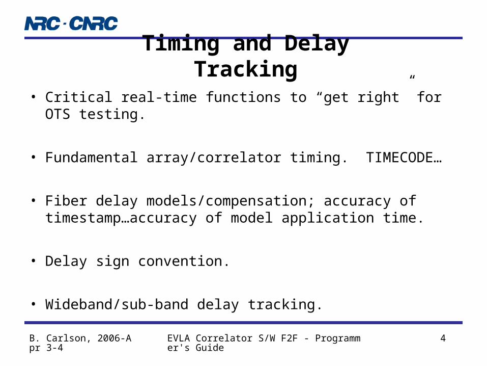
Timing and Delay Tracking
• Critical real-time functions to “get right” for OTS testing.
• Fundamental array/correlator timing. TIMECODE…
• Fiber delay models/compensation; accuracy of timestamp…accuracy of model application time.
• Delay sign convention.
• Wideband/sub-band delay tracking.

B. Carlson, 2006-Apr 3-4 EVLA Correlator S/W F2F - Programmer's Guide 5
Station Board
Delay Buffer(0.25 sec deep)
Antenna 1PPStime tick(A1PPS)
Array TimingReference
(GPS UTC +H-maser)
0.12 sec nominaldelay Synchronization
and delaytracking
TimecodeGenerator
Board
0.12 secdelay
Timing to Baseline/Phasing Boards
Set timeand delay
Baseline/PhasingBoards
TIM
ING
SY
NC
SynchronizedProcessing
Constant delays,geometric delays + LO
round-trip delay
System1PPS + 128MHz clock
LO reference
+ 1PPS tick
Correlator
TIMECODE(s)
TIMECODE
LO feedback
Fiber delay ~200 us(20 km)
LO round-trip phasemeasurement
Fiber delay ~200 us(20 km)
B. Carlson, 2006-Apr 3-4 EVLA Correlator S/W F2F - Programmer's Guide 6
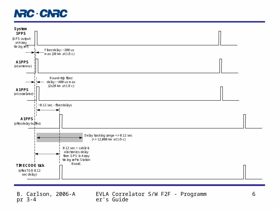
A1PPS(at antenna)
A1PPS(at correlator)
A1PPS(after delay buffer)
Round-trip fiberdelay: ~400 us max(2x20 km at 1/3 c)
Delay tracking range +/- 0.12 sec(+/- 12,000 km at 1/3 c)
System1PPS
(GPS outputat Array
timing ref)
TIMECODE tick(after TGB 0.12
sec delay)
~0.12 sec - fiber delays
Fiber delay: ~200 usmax (20 km at 1/3 c)
0.12 sec + cable &electronics delay
from GPS in Arraytiming ref to Station
Board.

B. Carlson, 2006-Apr 3-4 EVLA Correlator S/W F2F - Programmer's Guide 7
TIMECODE initialization/selection
128 MHz reference clock
Reference 1 PPS
Signals from ArrayTiming Reference
A-TIMECODE-0
A-TIMECODE-1
A-TIMECODE-2
B-TIMECODE-0
B-TIMECODE-1
B-TIMECODE-2
TIMECODE Set A(a.k.a. “Set 0”)
TIMECODE Set B(a.k.a. “Set 1”)
M&C Ethernet
TimecodeGenerator
FPGA
TimecodeGenerator
FPGA
Dec
oder
/Syn
cD
ecod
er/S
ync
TimecodeGenerator Board A
TimecodeGenerator Board B
All
Sta
tion
Boa
rds’
“T
imin
g C
hips
”
All
Bas
elin
e a
nd P
hasi
ng B
oard
s

B. Carlson, 2006-Apr 3-4 EVLA Correlator S/W F2F - Programmer's Guide 8
External Timecode from NRAO

B. Carlson, 2006-Apr 3-4 EVLA Correlator S/W F2F - Programmer's Guide 9
Correlator TIMECODE

B. Carlson, 2006-Apr 3-4 EVLA Correlator S/W F2F - Programmer's Guide 10
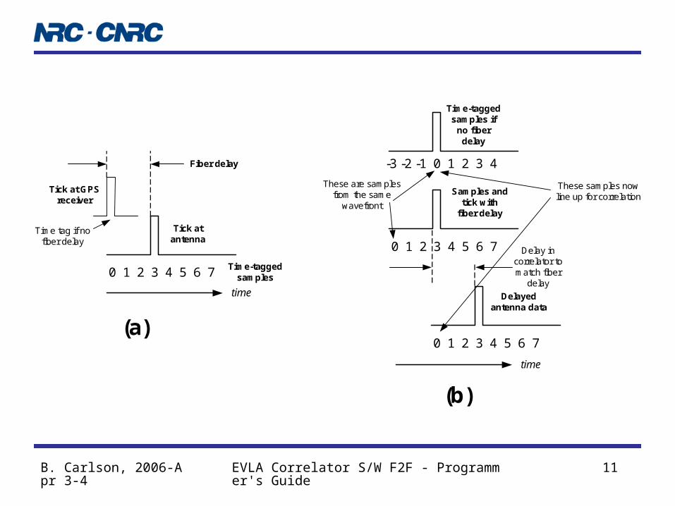
Fiber delay models
• Array Timing Reference-to-antenna fiber delays need to be known well enough to ensure that fringes are found within the delay search range of the correlator.– Min +/-250 nsec; max +/-32 usec for sub-band 128 MHz.
• Accuracy of fiber delay model for at least one antenna determines accuracy of timestamps and when models are applied in correlator.
• Fiber delays are put into the correlator as +’ve delay offsets.
B. Carlson, 2006-Apr 3-4 EVLA Correlator S/W F2F - Programmer's Guide 11
0 1 2 3 4 5 6 7
time
Fiber delay
Tick at GPSreceiver
Tick atantenna
Time-taggedsamples
-3 -2 -1 0 1 2 3 4
0 1 2 3 4 5 6 7
Time-taggedsamples if
no fiberdelay
Samples andtick with
fiber delay
These are samplesfrom the same
wavefront
0 1 2 3 4 5 6 7
Delayedantenna data
These samples nowline up for correlation
Delay incorrelator tomatch fiber
delay
Time tag if nofiber delay
time
(a)
(b)

B. Carlson, 2006-Apr 3-4 EVLA Correlator S/W F2F - Programmer's Guide 12
Delay sign convention
Direction of(+)’ve delay
Direction of(-)‘ve delay
tick wavefront timeat tick
Phase reference plane
Sourcevector
Phase reference:real or virtual
antenna
*Source
tick-tauX wavefronttime at tick
tick+tauY wavefronttime at tick
tauX
tauY
Station Y
Station X
Direction ofwavefront
propagation
B. Carlson, 2006-Apr 3-4 EVLA Correlator S/W F2F - Programmer's Guide 13
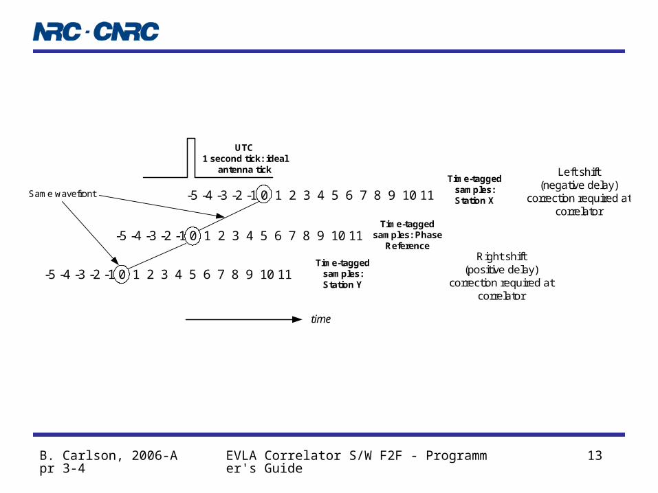
time
UTC1 second tick: ideal
antenna tickTime-tagged
samples:Station X
-5 -4 -3 -2 -1 0 1 2 3 4 5 6 7 8 9 10 11
-5 -4 -3 -2 -1 0 1 2 3 4 5 6 7 8 9 10 11
-5 -4 -3 -2 -1 0 1 2 3 4 5 6 7 8 9 10 11
Time-taggedsamples: Phase
Reference
Time-taggedsamples:Station Y
Same wavefront
Left shift(negative delay)
correction required atcorrelator
Right shift(positive delay)
correction required atcorrelator

B. Carlson, 2006-Apr 3-4 EVLA Correlator S/W F2F - Programmer's Guide 14
Delay Tracking
• Develop simplified model.
• Define the “Delay Tracker Quiescent State” to be when the A1PPS and the reference (TIMECODE) tick at output of delay buffer are lined up.– Sets value of Reference Pointer.
– Allows antenna-to-correlator fiber delays to be completely factored out.

B. Carlson, 2006-Apr 3-4 EVLA Correlator S/W F2F - Programmer's Guide 15
Delay Tracking—simple model
Delay FIFOBuffer
Antenna 1PPS(A1PPS) Delayed_A1PPS Measurement
Point
Reference 1PPS
Data InData Out
(to correlation)

B. Carlson, 2006-Apr 3-4 EVLA Correlator S/W F2F - Programmer's Guide 16
Delay tracking—actual model (simplified)
Wideband DelayFIFO Buffer
MeasurementPoint
Sub-band DelayFIFO Buffer
FIR Taps
TimingChip
TIMECODEs in
TIMECODE out
Data in Data out
A1PPSDelayedA1PPS
Constant½ Buffer
Delay
½ FIR TapDelay
Reference tick
Other filterchip
functions(Stage 2mixer,state
countsetc)
Sub-bandData out
Delay Module
Filter Chip
Output Interface toBaseline/Phasing
Boards
A
BC
B. Carlson, 2006-Apr 3-4 EVLA Correlator S/W F2F - Programmer's Guide 17
Delay Tracking
• Wideband: handled by the Delay Module.– H/W logic handles complexity of de-multiplexed data stream and
delay slewing; presents relatively simple software interface.– Concrete example given to go from floating-point point-slope model
to H/W register values.– Delay always specified in terms of number of 244 psec (244.140625)
units.
• Sub-band: handled by the Filter Chip (but operates on wideband data).– Similar to Delay Module, but only +/-16 usec.– Delay specified in terms of “samples at the original sample rate”.– Concrete example given…

B. Carlson, 2006-Apr 3-4 EVLA Correlator S/W F2F - Programmer's Guide 18
Delay Tracking
• Very fine delay tracking (+/-1/32 samples) handled and timed completely in hardware. S/W needs only to set where it is applied.
• Can be applied using the Filter Chip Stage 2 DSSB mixer or, in the Correlator Chip mixer (normally).– If applied in the Filter Chip, “PHASERR” going to the Baseline
Boards is forced to 0 by H/W.

B. Carlson, 2006-Apr 3-4 EVLA Correlator S/W F2F - Programmer's Guide 19
Delay Tracking
• M&C delivers models to the correlator with a “Model Server”.– Separate models for wideband delay and sub-band delay.
• Models:– Constant “clock model”…for constant LO distribution fiber delays.
– LO fiber round-trip delay model.
– Geometric delay model (CALC).
– Could do WVR measurements if desired…
• Convenient if model’s “to” in terms easily understood by the correlator (i.e. # seconds since Epoch – TIMECODE COUNTPPS).

B. Carlson, 2006-Apr 3-4 EVLA Correlator S/W F2F - Programmer's Guide 20
Phase Models and Fringe Rotation
• Earth-rotation phase, fiber round-trip phase, fshift phase.
• Normally applied in Correlator Chip.– Could be partially or completely applied in Filter Chip DSSB mixer
but lose benefit of doing it at the last possible point (and mixer band-edge degradation).
• “t” of calculation depends on:– Delay through Filter Chip stages…measured for each Filter Chip in
the Output Chip of the Station Board.
– Recirculation parallel or serial phase.

B. Carlson, 2006-Apr 3-4 EVLA Correlator S/W F2F - Programmer's Guide 21
LOo
LOo + fshift
frequency
ampl
itude
phas
e
tau(t) = dphi/df
phi_BB(t)
phi_RF(t)phi_net(t)
LOo + fshift

B. Carlson, 2006-Apr 3-4 EVLA Correlator S/W F2F - Programmer's Guide 22
Phase Models and Fringe Rotation
• Calculation is:
• Concrete example given…– Net_LO includes the fshift, and thus is different for each antenna.
– How to calculate P0 and P1 PHASEMOD coefficients.
– How to build the PHASEMOD frame—HES—Hardware Executable Script. Written to Timing Chip on Station Board.
tfshiftLONettt )_()()(

B. Carlson, 2006-Apr 3-4 EVLA Correlator S/W F2F - Programmer's Guide 23
0 1 0 01 PLEN BB0 SB0 P0-0 P1-0 BBk SBk P0-k P1-k CRC-4 010 1
Start bit(a lways 0 )
PLEN : Num ber o f phase po lynom ia lde finitions tha t fo llow. This is equa lto k+1 . (8 b its)
P hase po lynom ia lde finition 0 (72 b its)
P hase po lynom ia lde finition k (72 b its)
C R C -4: 4 -b it C RC to be ca lcula ted onon a ll b its from P LE N to P 1-k inc lus ive .The genera to r po lynom ia l is :P (x) = x^4 + x + 1 (o r, thegenera to r pa tte rn is 10011)
A lways '0'
pream b le (0101 ...)
tim e
B aseband # (0...7)tha t this po lynom ia lis app licab le to (3 b its)
Sub-band # (0...17)tha t this po lynom ia lis app licab le to (5 b its).
P0: Ze ro -th o rde r phasete rm (i.e . initia l phase).32 -b its rep resenting1 cyc le o f phase .
P1: F irs t o rde r phasete rm (i.e . phase ra te ).32 -b its (2 's com p lem ent)rep resenting +/-1 cyc le /sam p le . NOTE :
1 . P o lynom ia l coe ffic ients ge tloaded and a re active on theTIM E C OD E 'T' b it (100P P S )tha t occurs a fte r this fram e.2 . M ultip le P HA S E M OD fram escan be de fined be fo re a 'T' b it.
PHASEMOD Format
SID
8-b it S ta tion ID

B. Carlson, 2006-Apr 3-4 EVLA Correlator S/W F2F - Programmer's Guide 24
Command Tx Data Width Data
0123456789101112131415
Command [15:11]
Command Name
Action
00000 N/A Reserved. Ignored by the executor. 00001 SBIT Generate a Start Bit. Effectively generates a ‘100’ output. 00010 FOD Generate Width bits of Data 00011 CRC Generate a 4-bit CRC 00100 END Stop execution, continuously generate Preamble
(101010…), and wait for 10-msec tick to come along before executing the next Command written to the other RAM. Once the microprocessor writes an END Command, it must not write any more Commands until after the next 10-msec tick.
1xxxx NOP Generate a defined count+1 of the ‘10’ pattern. Here, count is bits 0-14 of this word.
All others N/A Reserved for future use. Ignored by the executor.

B. Carlson, 2006-Apr 3-4 EVLA Correlator S/W F2F - Programmer's Guide 25
Cmd Width Data Description NOP Count=99 100 Preambles to ensure first frame occurs well after the 10-
msec tick. SBIT n/a n/a Start bit ‘100’ output FOD 111 0x01 PLEN=1; this frame contains one PHASEMOD FOD 111 0x55 SID=0x55 FOD 010 0x3 Baseband=3 FOD 100 0x10 Sub-band=16 FOD 111 0xFB P0—Byte 0 FOD 111 0x3F P0—Byte 1 FOD 111 0x86 P0—Byte 2 FOD 111 0x32 P0—MSByte 3 FOD 111 0x5D P1—Byte 0 FOD 111 0xF1 P1—Byte 1 FOD 111 0xF4 P1—Byte 2 FOD 111 0xFF P1—MSByte 3 CRC n/a na/ CRC-4 code NOP Count=9 Insert some Preamble for good measure Other PHASEMOD frames… END Count=31959 Preamble Fill

B. Carlson, 2006-Apr 3-4 EVLA Correlator S/W F2F - Programmer's Guide 26
CMIB writes Phasemodel script to
PMPort_R for allPHASEMODs to be
generated
time
0 10 msec 20 msec 30 msec
PHASEMOD framestransmitted by
executor toBaseline/Phasing
Boards
New Phasemodels take
effect
CMIB gets interrupt

B. Carlson, 2006-Apr 3-4 EVLA Correlator S/W F2F - Programmer's Guide 27
Phase Models and Fringe Rotation
• Each Station Board CMIB must write phase models (i.e. build PHASEMOD) for all of its own outputs.
• Other models may be present, but they are ignored by downstream hardware.

B. Carlson, 2006-Apr 3-4 EVLA Correlator S/W F2F - Programmer's Guide 28
Dump Control
• Station Board generates the DUMPTRIG signal to control all down-stream dumping/integration for the Correlator Chip and the LTA.
• Sub-array/correlator-wide synchronization required to support recirculation and phase binning.– One way or another, synchronize to TIMECODE to eliminate Station
Board-to-Station Board communication.
• HES built by S/W to generate DUMPTRIG.
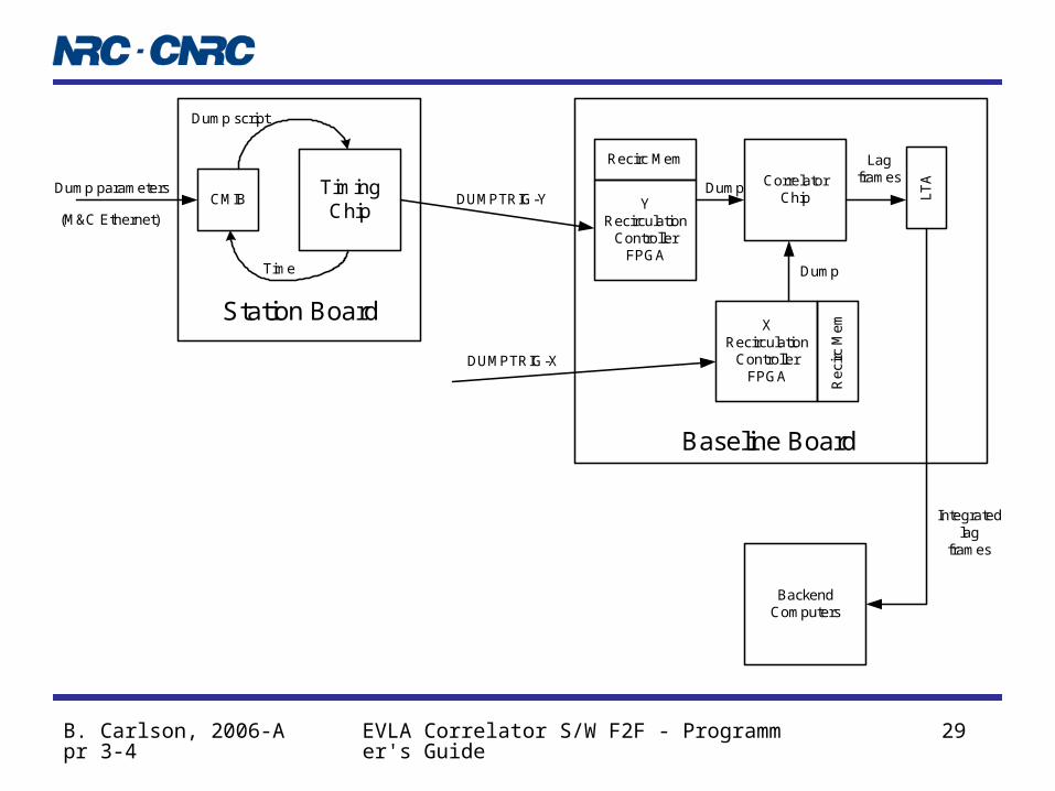
B. Carlson, 2006-Apr 3-4 EVLA Correlator S/W F2F - Programmer's Guide 29
Station Board
TimingChip
Baseline Board
YRecirculation
ControllerFPGA
XRecirculation
ControllerFPGA
CorrelatorChip
Recirc Mem
Re
circ
Me
m
DUMPTRIG-Y
DUMPTRIG-X
CMIB
Dump script
Time
Dump parameters
(M&C Ethernet)
LTA
Lagframes
Dump
Dump
BackendComputers
Integratedlag
frames

B. Carlson, 2006-Apr 3-4 EVLA Correlator S/W F2F - Programmer's Guide 30
0 1 0 0 CRC-4DLEN BB0 SB0 BB1 SB1 BBk SBk PBCMD 1 10 10 1 1 01
tim e
preamble (0101...)
S tart b it(always 0)
D u m p specificatio nlen g th (8 b its):The number of BBand SB pairs definedin this frame. This isequal to k+1. B aseb an d # to du m p (5 b its):
11111 -- A ll basebands00xxx -- Baseband ID (0...7)
S ub -band # to d um p (5 b its):11111 -- A ll sub-bandsothers -- Sub-band ID (0...17)
BB/SBpair 0
BB/SBpair 1
BB/SBpair k
P h ase b in # (16 b its):The LTA (phase) binnumber that the datais to be dumped into.The MSB of this wordis the bank #. Eachdump must specify anLTA/phase bin numberto put the data into evenif pulsar phase binningis not formally active.
D u m p C om m an d (3 b its):000 -- First dump of data into LTA bin. Just save data in LTA bin.001 -- Add data to existing LTA data and save in LTA bin.010 -- Last dump: add to LTA data; flag LTA bin as ready.011 -- Speed dump: bypass LTA directly to output.100 -- Dump data and discard it. This clears the correlator chip accumulators.101 -- S ingle dump: save in LTA and flag bin as ready.110 -- Reset the recirculation block counter to the start block. No dump action taken.111 -- Synchronization test frame. Dump Trigger is generated and is aligned with the 'T' bit of TIMECODE. No dump action taken
C R C -4: 4-bit CRC to be calculated onon all bits from CMD to PB inclusive.The generator polynomial is:P(x) = x^4 + x + 1 (or, thegenerator pattern is 10011)
D um p T rig g er:Data is dumpedand timestampedon this bit (2nd '1'in a row) after asuccessful DUMPTRIGframe.A lw ays '1 '
D U M P TR IG F o rm at
NOTES:1. Multiple DUMPTRIG frames can be defined before each Dump Trigger.2. Must have at least 4 preamble bits between DUMPTRIG frames.
additional DUMPTRIGframes
TID
Trig ger ID (4 b its)Frames with thesame TID have thesame Dump Trigger
SID
8-b it S tatio n ID
A lw ays '0 '
FRAME
B. Carlson, 2006-Apr 3-4 EVLA Correlator S/W F2F - Programmer's Guide 31
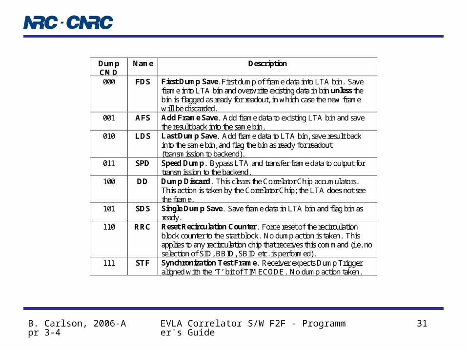
Dump CMD
Name Description
000 FDS First Dump Save. First dump of frame data into LTA bin. Save frame into LTA bin and overwrite existing data in bin unless the bin is flagged as ready for readout, in which case the new frame will be discarded.
001 AFS Add Frame Save. Add frame data to existing LTA bin and save the result back into the same bin.
010 LDS Last Dump Save. Add frame data to LTA bin, save result back into the same bin, and flag the bin as ready for readout (transmission to backend).
011 SPD Speed Dump. Bypass LTA and transfer frame data to output for transmission to the backend.
100 DD Dump Discard. This clears the Correlator Chip accumulators. This action is taken by the Correlator Chip; the LTA does not see the frame.
101 SDS Single Dump Save. Save frame data in LTA bin and flag bin as ready.
110 RRC Reset Recirculation Counter. Force reset of the recirculation block counter to the start block. No dump action is taken. This applies to any recirculation chip that receives this command (i.e. no selection of SID, BBID, SBID etc. is performed).
111 STF Synchronization Test Frame. Receiver expects Dump Trigger aligned with the ‘T’ bit of TIMECODE. No dump action taken.
B. Carlson, 2006-Apr 3-4 EVLA Correlator S/W F2F - Programmer's Guide 32
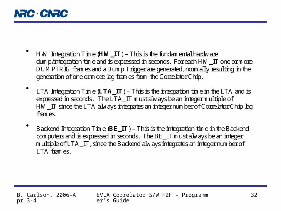
H/W Integration Time (HW_IT) – This is the fundamental hardware dump/integration time and is expressed in seconds. For each HW_IT one or more DUMPTRIG frames and a Dump Trigger are generated, normally resulting in the generation of one or more lag frames from the Correlator Chip.
LTA Integration Time (LTA_IT) – This is the integration time in the LTA and is expressed in seconds. The LTA_IT must always be an integer multiple of HW_IT since the LTA always integrates an integer number of Correlator Chip lag frames.
Backend Integration Time (BE_IT) – This is the integration time in the Backend computers and is expressed in seconds. The BE_IT must always be an integer multiple of LTA_IT, since the Backend always integrates an integer number of LTA frames.

B. Carlson, 2006-Apr 3-4 EVLA Correlator S/W F2F - Programmer's Guide 33
For each stream (a stream being the output of a Digital Filter on the Station Board), there can be a different HW_IT. However, there is a hardware restriction in that every HW_IT must be an integer multiple of the smallest HW_IT that is in DUMPTRIG.
HW_ITmax is 500 sec. A larger HW_IT may result in overflow of the Correlator Chip accumulators.

B. Carlson, 2006-Apr 3-4 EVLA Correlator S/W F2F - Programmer's Guide 34
Dump Modes
• Normal dump-and-integrate.
• Recirculation dump-and-integrate.– Recirc FPGA on Baseline Board handles all counting, memory pointer
offsets etc. Driven by Dump Triggers and CMDs.
• Phase binning.
• Recirculation and phase binning .
• Burst dumping.

B. Carlson, 2006-Apr 3-4 EVLA Correlator S/W F2F - Programmer's Guide 35
Normal dump-and-integrate
CMD Time Phase bin Bank Action DD 0 X X Dump/discard. Clears accumulators FDS 500 us 0 0 First dump into LTA AFS 1 ms 0 0 Add to LTA AFS 1.5 ms 0 0 Add to LTA AFS 2.0 ms 0 0 Add to LTA AFS 2.5 ms 0 0 Add to LTA LDS 3.0 ms 0 0 Add to LTA, flag as ready FDS 3.5 ms 1 0 First dump into LTA AFS 4 ms 1 0 Add to LTA AFS 4.5 ms 1 0 Add to LTA AFS 5.0 ms 1 0 Add to LTA AFS 5.5 ms 1 0 Add to LTA LDS 6.0 ms 1 0 Add to LTA, flag as ready FDS 6.5 ms 2 0 First dump into LTA … … … …

B. Carlson, 2006-Apr 3-4 EVLA Correlator S/W F2F - Programmer's Guide 36
Recirculation dump-and-integrateCMD Time Phase bin Bank Lags Action DD 0 X X N/A Dump/discard. Clears corr chip
accumulators. RRC 0 X X N/A Force reset of recirc. block counter FDS 500 us 0 0 0-127 First dump of data into LTA FDS 1 ms 0 0 128-255 First dump of data into LTA FDS 1.5 ms 0 0 256-383 First dump of data into LTA FDS 2.0 ms 0 0 384-511 First dump of data into LTA RRC 2.0 ms X X N/A Force reset of recirc. block counter AFS 2.5 ms 0 0 0-127 Add to LTA AFS 3.0 ms 0 0 128-255 Add to LTA AFS 3.5 ms 0 0 256-383 Add to LTA AFS 4.0 ms 0 0 384-511 Add to LTA RRC 4.0 ms X X N/A Force reset of recirc. block counter LDS 4.5 ms 0 0 0-127 Add to LTA, flag as ready LDS 5.0 ms 0 0 128-255 Add to LTA, flag as ready LDS 5.5 ms 0 0 256-383 Add to LTA, flag as ready LDS 6.0 ms 0 0 384-511 Add to LTA, flag as ready RRC 6.0 ms X X N/A Force reset of recirc. block counter FDS 6.5 ms 1 0 0-127 First dump of data into LTA FDS 7.0 ms 1 0 128-255 First dump of data into LTA FDS 7.5 ms 1 0 256-383 First dump of data into LTA FDS 8.0 ms 1 0 384-511 First dump of data into LTA RRC 8.0 ms X X N/A Force reset of recirc. block counter AFS 8.5 ms 1 0 0-127 Add to LTA … … … … … …

B. Carlson, 2006-Apr 3-4 EVLA Correlator S/W F2F - Programmer's Guide 37
X
Y
Lag B lock: 0 1 2 3 4 5 6 7
X R e c irc B lo c k: 7 6 5 4 3 2 1 0
Y R e c irc B lo c k: 0 1 2 3 4 5 6 7
cente r lag=N/2
Lag 0
Lag N-1
N-lag Correlator Recircu lation B lock Nu m b erin g(for case of N=32, b lock s ize = 4 lag s)
older Y samples
older X samples

B. Carlson, 2006-Apr 3-4 EVLA Correlator S/W F2F - Programmer's Guide 38
Phase binning
CMD Time Phase bin Bank Action DD 0 X X Dump/discard. Clears corr chip accumulators. FDS 250 s 0 0 First dump bin 0 FDS 500 s 1 0 First dump bin 1 FDS 750 s 2 0 First dump bin 2 FDS 1 ms 3 0 First dump bin 3 FDS 1.25 ms 4 0 First dump bin 4 AFS 1.5 ms 0 0 Add to LTA bin 0 AFS 1.75 ms 1 0 Add to LTA bin 1 AFS 2 ms 2 0 Add to LTA bin 2 AFS 2.25 ms 3 0 Add to LTA bin 3 AFS 2.5 ms 4 0 Add to LTA bin 4 AFS 2.75 ms 0 0 Add to LTA bin 0 AFS 3 ms 1 0 Add to LTA bin 1 AFS 3.25 ms 2 0 Add to LTA bin 2 AFS 3.5 ms 3 0 Add to LTA bin 3 AFS 3.75 ms 4 0 Add to LTA bin 4 LDS 4 ms 0 0 Add to LTA, flag as ready bin 0 LDS 4.25 ms 1 0 Add to LTA, flag as ready bin 1 LDS 4.5 ms 2 0 Add to LTA, flag as ready bin 2 LDS 4.75 ms 3 0 Add to LTA, flag as ready bin 3 LDS 5 ms 4 0 Add to LTA, flag as ready bin 4 FDS 5.25 0 1 First dump bin 0, bank 1 … … … … …
B. Carlson, 2006-Apr 3-4 EVLA Correlator S/W F2F - Programmer's Guide 39
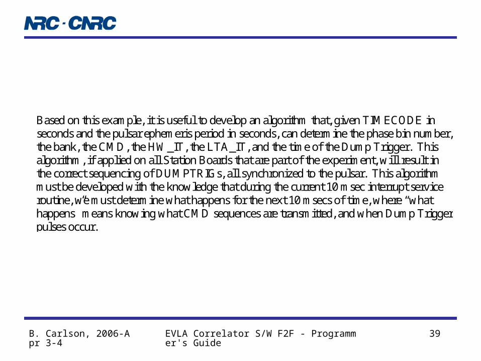
Based on this example, it is useful to develop an algorithm that, given TIMECODE in seconds and the pulsar ephemeris period in seconds, can determine the phase bin number, the bank, the CMD, the HW_IT, the LTA_IT, and the time of the Dump Trigger. This algorithm, if applied on all Station Boards that are part of the experiment, will result in the correct sequencing of DUMPTRIGs, all synchronized to the pulsar. This algorithm must be developed with the knowledge that during the current 10 msec interrupt service routine, we must determine what happens for the next 10 msecs of time, where “what happens” means knowing what CMD sequences are transmitted, and when Dump Trigger pulses occur.

B. Carlson, 2006-Apr 3-4 EVLA Correlator S/W F2F - Programmer's Guide 40
timetTC
TP
Nbin = 8
Tbin
tpulsar tpulsar tpulsar tpulsar tpulsar tpulsar
tDT0
tDT1
tDT2
tcalc3
0 1 2 3 4 5 6 7 0 1 2 3 4 5 6 7 0 1 2 3 4 5 6 7 0 1 2 3 4 5 6 7 0 1 2 3 4 5 6 7 0 1 2 3 4 5 6Phase bin:
TP x Bins_to_add
TP x Bins_to_add x 2
BANK 0 BANK 1CMD=FDS CMD=AFS CMD=LDS CMD=FDS CMD=AFS CMD=LDS
10 ms tick
S/W ISR builds HEDSfor next 10 msec period
TIMECODE10 ms tick 10 ms tick 10 ms tick
tbank
CMDinterval = 0 CMDinterval = 1 CMDinterval = 2 CMDinterval = 0 CMDinterval = 1 CMDinterval = 2
tbank
Pulsar pulse train

B. Carlson, 2006-Apr 3-4 EVLA Correlator S/W F2F - Programmer's Guide 41
Phase binning and recirculation
• Almost too painful to contemplate.
• Lose “recirculation factor” number of Phase bins– E.g. if recirculation factor is 4, then there are 1000/4=250 phase bins
available.
– “number of places to put data in LTA” is always constant.
– Left as an exercise for the reader to develop the S/W algorithm to implement.

B. Carlson, 2006-Apr 3-4 EVLA Correlator S/W F2F - Programmer's Guide 42
CMD Time Phase bin Bank Action DD 0 X X Dump/discard. Clears corr chip accumulators.
Resets recirc block counter. FDS 250 s 0 0 First dump bin 0 – recirc block 0 FDS 500 s 0 0 First dump bin 0 – recirc block 1 FDS 750 s 0 0 First dump bin 0 – recirc block 2 FDS 1.0 ms 0 0 First dump bin 0 – recirc block 3 RRC 1.0 ms X X Force reset of recirc block counter FDS 1.25 ms 1 0 First dump bin 1 – recirc block 0 FDS 1.5 ms 1 0 First dump bin 1 – recirc block 1 FDS 1.75 ms 1 0 First dump bin 1 – recirc block 2 FDS 2.0 ms 1 0 First dump bin 1 – recirc block 3 RRC 2.0 ms X X Force reset of recirc block counter FDS 2.25 ms 2 0 First dump bin 2 – recirc block 0 FDS 2.5 ms 2 0 First dump bin 2 – recirc block 1 FDS 2.75 ms 2 0 First dump bin 2 – recirc block 2 FDS 3.0 ms 2 0 First dump bin 2 – recirc block 3 RRC 3.0 ms X X Force reset of recirc block counter LDS 3.25 ms 0 0 Add to LTA bin 0 – recirc block 0 LDS 3.5 ms 0 0 Add to LTA bin 0 – recirc block 1 LDS 3.75 ms 0 0 Add to LTA bin 0 – recirc block 2 LDS 4.0 ms 0 0 Add to LTA bin 0 – recirc block 3 RRC 4.0 ms X X Force reset of recirc block counter … … … … …

B. Carlson, 2006-Apr 3-4 EVLA Correlator S/W F2F - Programmer's Guide 43
Burst Dumping
• Used when integration time is too small to allow for contiguous data capture.
• 3 ways of doing it:– Explicit control and synchronization of DUMPTRIG.
– Explicit control of LTA’s burst-mode.
– Implicit—let rate at which GigE chip can transmit data to Backend automatically control bursts.
• LTA fills up…priority naturally transfers to LTA-to-GigE data transfer.
• What data acquired for what baselines at what time is indeterminate.

B. Carlson, 2006-Apr 3-4 EVLA Correlator S/W F2F - Programmer's Guide 44
DUMPTRIG Synchronization
• Important for recirculation to ensure X/Y memory offset pointers correct.
• Correlator Chip XSTATUS, YSTATUS, and DESSR registers indicate if X/Y dump pulses not synchronized.– If not, it means that the lags being acquired for a particular lag block
are indeterminate.

B. Carlson, 2006-Apr 3-4 EVLA Correlator S/W F2F - Programmer's Guide 45
DUMPTRIG HES ExampleCmd Width Data #bits
@ 128 Mbps
#bits (elapsed)
Description
TRIG n/a n/a 2 2 Dump Trigger @ TIMECODE T-bit NOP Count=9 20 22 Preamble SBIT n/a n/a 3 25 Start bit ‘100’ output FOD 010 0x00 3 28 CMD=000; First dump. FOD 111 0x01 8 36 DLEN=1 FOD 011 0x00 4 40 TID=0 FOD 111 0x23 8 48 SID=0x23 FOD 100 0xFF 5 53 BB0=0xFF; all basebands FOD 100 0xFF 5 58 SB0=0xFF; all sub-bands FOD 111 0x80 8 66 Phase Bin MSByte=0, Bank=1 FOD 111 0x03 8 74 Phase Bin LSByte=3 CRC n/a na/ 4 78 CRC-4 code NOP Count=31959 63920 63998 Preamble Fill TRIG n/a na/ 2 64000 Dump Trigger at t=500.0 sec
Repeat above, CMD=001
63998 127998 Dump Trigger at t1.0 msec
Repeat 18 more times. Last CMD=010. END n/a n/a na/ End of script TRIG n/a n/a n/a Dump Trigger @ TIMECODE T-bit Other Commands for other frames.

B. Carlson, 2006-Apr 3-4 EVLA Correlator S/W F2F - Programmer's Guide 46
Station Board
• Overall functional description.
• Descriptions of chip functions from S/W perspective.
• Some blanks need to be filled in as some FPGA designs need upgrade or are in flux.
• References to documentation…

B. Carlson, 2006-Apr 3-4 EVLA Correlator S/W F2F - Programmer's Guide 47
InputChip
Delay Module 0
Delay Module 1
WidebandCorrelator
Filter Bank0
Filter Bank1
TimingChip
OutputChip 0
OutputChip 1
VSI Chip 0
VSI Chip 1
Mid
dle
conn
ecto
rT
op c
onne
ctor
Bot
tom
con
nect
or
Fib
er-o
ptic
mod
ule
&co
nnec
tor
CMIB/PCMC
Fib
ers
from
ant
enna
TIM
EC
OD
E
PH
AS
ER
R
PH
AS
ER
R
Widebandfractional
delay error
18
wa
fers
ou
t2x
TIM
EC
OD
Ew
afe
rs in
VS
I-H
I/O
or
HM
Gb
ps I/
OV
SI-
H I
/O o
r H
M G
bps
I/O
a
b
c
A/0
B/1
Widebandfractional
delay error

B. Carlson, 2006-Apr 3-4 EVLA Correlator S/W F2F - Programmer's Guide 48
Sub-bandbeam delay
trackingmemory
(8k deep)
Stage 4 FilterFIR
(64-512 taps)(31.25 kHz to
256 kHz)
01
2
15
Stage 1 Filter512-tap
Poly-phase FIR(~16 MHz to
128 MHz)
Stage 2 FilterFIR
(64-512 taps)+
DSSB mixer(8 MHz to64 MHz)
Stage 3 FilterFIR
(64-512 taps)(512 kHz to
4 MHz)
SidebandFlipper
4/7-bitrequantizer
Pre-requantizer
powerdetector(2 bins)
Fast interferencedetector and
data validblanking with
dwell time
01
2
15
Wideband delaytracking error
4/7-bit outputDelay-to-phase
conversion
Final residualdelay error
PHASERR
Inp
ut
fro
m W
ideb
and
Co
rrel
ato
r F
PG
A
Wideband data:16 x 4-bits @ 256
Mwords/sec
Filtered data,16-bits wide
Noise diodebin control
Data validqualifer
Data valid
Narrow-bandsub-sample
delay correction
Datavalid
encoding
Powerdetector,
state counts,phase-caldetector
To
Ou
tpu
t C
hip
, Tim
ing
Ch
ip, V
SI C
hip
ClipCounter

B. Carlson, 2006-Apr 3-4 EVLA Correlator S/W F2F - Programmer's Guide 49
Station Board Data Products
• Wideband state counts.• Wideband correlation lags.• 16-bit stage output clip counter.• Pre-re-quantizer power measurement.• Re-quantizer state counts.• Re-quantizer power.• Re-quantizer clip counter.• Tone extractor I&Q.• RFI blanker counter.• Radar-mode data capture.

B. Carlson, 2006-Apr 3-4 EVLA Correlator S/W F2F - Programmer's Guide 50
Station Board miscl
• Memory map.
• PCMC– Processor boot, PCI devices, absolute memory addresses.
– FPGA programming (“personality” programming). Byte-wide.
– A/D readings for V + T monitor.
– 10 msec interrupt.

B. Carlson, 2006-Apr 3-4 EVLA Correlator S/W F2F - Programmer's Guide 51
Baseline Board
• Overall description.
• Important points of note for each chip…details refer to RFS docs.
• Mostly configuration and monitor. Relatively little real-time S/W.

B. Carlson, 2006-Apr 3-4 EVLA Correlator S/W F2F - Programmer's Guide 52
‘Y’Recirculation
ControllerFPGA 2
‘Y’Recirculation
ControllerFPGA 1
‘Y’Recirculation
ControllerFPGA 0
‘X’Recirculation
ControllerFPGA 0
‘X’Recirculation
ControllerFPGA 1
‘X’Recirculation
ControllerFPGA 2
CorrelatorChip
LTA
Con
tro
ller
CorrelatorChip
LTA
Con
tro
ller
CorrelatorChip
LTA
Con
tro
ller
CorrelatorChip
LT
AC
ontr
olle
r
CorrelatorChip
LT
AC
ontr
olle
r
CorrelatorChip
LT
AC
ontr
olle
r
CorrelatorChip
LT
AC
ontr
olle
r
CorrelatorChip
LT
AC
ontr
olle
r
CorrelatorChip
LT
AC
ontr
olle
rGigEChip
To
p C
onn
ecto
rB
ott
om C
onn
ect
or
HM 1 Gbps
HM 1 Gbps
GigE toBackend
Inp
uts
fro
m S
tatio
n B
oa
rds
Inp
uts
fro
m S
tatio
n B
oa
rds
DP
SR
AM
DP
SR
AM
DP
SR
AM
DPSRAM
DPSRAM
DPSRAM
Row 0
Row 1
Row 2
Col 0Col 1Col 2

B. Carlson, 2006-Apr 3-4 EVLA Correlator S/W F2F - Programmer's Guide 53
HM
Gbp
s R
ecei
vers
Inp
ut C
ross
-ba
r S
witc
h
Out
put
Da
ta P
ath
Sw
itch
Tes
t Ve
cto
r S
witc
h
Re
circ
ula
tion
Se
lect
ion
Sw
itch
Recirculator
4 x
HM
Gb
ps W
afe
rsfr
om S
tatio
n B
oard
s
Da
ta, P
has
e, C
ontr
olO
utp
uts
to C
orr
ela
tor
Ch
ips
“internal” data streams
ExternalDPSRAM
Bit Force
Au
to-c
orre
lato
r M
ode
Sel
ect
Test VectorGenerator

B. Carlson, 2006-Apr 3-4 EVLA Correlator S/W F2F - Programmer's Guide 54
CCQ-0(4x128 Clags)
CCQ-1(4x128 Clags)
CCQ-2(4x128 Clags)
CCQ-3(4x128 Clags)
X-STR[0]-in
Dump Gen/ID Capture
MCB_ADDR[0:3]MCB_DATA[0:7]MCB_CS_MCB_RD/WR_MCB_CLKRESET_
DATA_CS_DATA_RDY_ACCDATA[0:31]DATA_OE_DATA_CLKOUTDATA_VALID_FRAME_ABORT_
Simplified Correlator Chip Block Diagram
LTAControllerInterface
uP/MCBInterface
X-CLOCK-in Y-CLOCK-in
X In
put F
IFO
Buf
fer
(92-
bit x
64
deep
)
Y In
put F
IFO
Buf
fer
(92-
bit x
64
deep
)
ReadoutControl/LTA I/F
MCBInterface
X Data/Control
Y Data/Control
PLL PLL
X-STR[0]-out
X-STR[1]-in
X-STR[1]-out
X-STR[2]-in
X-STR[2]-out
X-STR[3]-in
X-STR[3]-out
X-STR[4]-in
X-STR[4]-out
X-STR[5]-in
X-STR[5]-out
X-STR[6]-in
X-STR[6]-out
X-STR[7]-in
X-STR[7]-out
X-CTRL-in
X-CTRL-out
X-CLOCK-out Y-CLOCK-out
Y-STR[0]-in
Y-STR[0]-out
Y-STR[1]-in
Y-STR[1]-out
Y-STR[2]-in
Y-STR[2]-out
Y-STR[3]-in
Y-STR[3]-out
Y-STR[4]-in
Y-STR[4]-out
Y-STR[5]-in
Y-STR[5]-out
Y-STR[6]-in
Y-STR[6]-out
Y-STR[7]-in
Y-STR[7]-out
Y-CTRL-in
Y-CTRL-out
TDI TMS TCK TDO
JTAG Interface
Auto-corrSwitch
PLL_RESET_
TESTMODE_0
TESTMODE_1
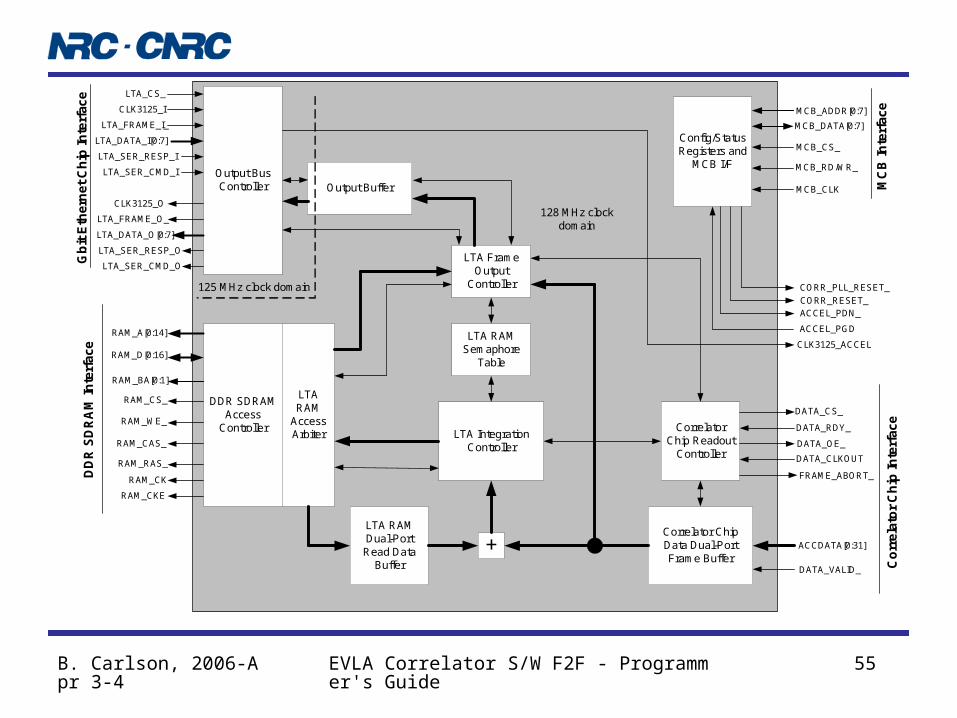
B. Carlson, 2006-Apr 3-4 EVLA Correlator S/W F2F - Programmer's Guide 55
LTA IntegrationController
CorrelatorChip Readout
Controller
Correlator ChipData Dual-PortFrame Buffer
LTA RAMDual-PortRead Data
Buffer
DDR SDRAMAccess
Controller
LTA RAMSemaphore
Table
LTA FrameOutput
Controller
Output BufferOutput BusController
LTARAM
AccessArbiter
Config/StatusRegisters and
MCB I/F
+
MCB_ADDR[0:7]
MCB_DATA[0:7]
MCB_CS_
MCB_RD/WR_
MCB_CLK
ACCDATA[0:31]
DATA_CS_
DATA_RDY_
DATA_OE_
DATA_CLKOUT
FRAME_ABORT_
DATA_VALID_
CLK3125_I
LTA_CS_
LTA_FRAME_I_
LTA_DATA_I[0:7]
RAM_D[0:16]
RAM_A[0:14]
RAM_BA[0:1]
RAM_CS_
RAM_WE_
RAM_CAS_
RAM_RAS_
RAM_CK
RAM_CKE
Gb
it E
the
rne
t C
hip
Inte
rfac
eD
DR
SD
RA
M In
terf
ace
Co
rre
lato
r C
hip
Inte
rfa
ce
MC
B In
terf
ac
e
125 MHz clock domain
128 MHz clockdomain
LTA_SER_CMD_I
LTA_SER_RESP_I
CLK3125_O
LTA_FRAME_O_
LTA_DATA_O[0:7]
LTA_SER_CMD_O
LTA_SER_RESP_O
ACCEL_PDN_
ACCEL_PGD
CLK3125_ACCEL
CORR_RESET_
CORR_PLL_RESET_

B. Carlson, 2006-Apr 3-4 EVLA Correlator S/W F2F - Programmer's Guide 56
DP FrameBuffer-H
DP FrameBuffer-L
LTA_SER_CMD[0:7]
LTA_CS_[0:63]
EthernetFrame Builder
Scheduler
8B/10B Encoder,Serializer
(specializedFPGA functions)
Gbit/sec Ethernetinput
Dest. IPAddresses+ Enables
Config/StatusRegisters and
MCB I/F
MCB_ADDR[0:7]
MCB_DATA[0:7]
MCB_CS_
MCB_RD/WR_
MCB_CLK
ClockGenerator
PLL
CLK125_in
Internal 125 MHz clock
8 External 31.25 MHz clocks
CO
L #
0
LTA_DATA[0:7]
LTA_FRAME_
LTA_SER_RESP
DD
R In
put
LTA_DATA[0:7]
LTA_FRAME_
LTA_SER_RESP
DD
R In
put
LTA_DATA[0:7]
LTA_FRAME_
LTA_SER_RESP
DD
R I
nput
CO
L #
1C
OL
#2
LTA_DATA[0:7]
LTA_FRAME_
LTA_SER_RESP
DD
R In
put
CO
L #
7
LTA_SER_RESP-H
LTA_SER_RESP-L
Checksum Calc
LTA_SER_CMD_RET[0:7]
Gbit/sec Ethernetoutput
GBIT_CFG[2:0]

B. Carlson, 2006-Apr 3-4 EVLA Correlator S/W F2F - Programmer's Guide 57
Preamble SFD DATA CRC-32
7 1
6 6
2 584 or 1096 4
10101010 10101010 10101010 10101010 10101010 10101010 10101010
10101011
Covered by CRC-32
Vers HL
Type
Length
Identification Flg Fragment Offset
TTL Protocol Header Checksum
Source IP Address
Destination IP Address
0 31
0 31
Start Sync (101010…)
Start_BlockY NBlocks nlags ChipID CCC FType
BBIDY SBIDY SID-Y BBIDX SBIDX SID-X
CHECKSUM
IP Header(20 bytes)
Length Checksum
LTA Data Frame(556 or 1068 bytes)
31 0
UDP Header(8 bytes)
IEEE 802.3 Ethernet Frame with UDP/IP and LTA Data Frametime
Destination Address Source Address
Type
Source Port Destination Port
Type/Length

B. Carlson, 2006-Apr 3-4 EVLA Correlator S/W F2F - Programmer's Guide 58
Baseline Board miscl
• Memory map.
• PCMC– Similar to Station Board (Processor boot, PCI devices).
– FPGA programming…bit serial.
– A/D V+T readings.
– All Corr Chip core voltages accessed using one A/D channel and dual 32:1 analog switches. Use Recirc-Y7 to control analog switches.
– 10 msec interrupt.
• Correlator Chip power and reset sequencing.– Controlled thru regs on companion LTA.
– Power sequence, PLL reset sequence, reset sequence.

B. Carlson, 2006-Apr 3-4 EVLA Correlator S/W F2F - Programmer's Guide 59
Other Boards
• Timecode Board and Phasing Board.– Details still to be filled in…
B. Carlson, 2006-Apr 3-4 EVLA Correlator S/W F2F - Programmer's Guide 60
System
• Remote power monitor and control.• M&C network.• Baseline Board to CBE GigE switched network.• Station-to-Baseline Board data routing.
– Mechanical mock-up demonstrates that cable routing in Baseline rack is feasible.
• Location of Phasing Board not completely defined.– In Baseline racks?– In separate rack?
• System module numbering and identification: ICD A25010N0002.

B. Carlson, 2006-Apr 3-4 EVLA Correlator S/W F2F - Programmer's Guide 61
X / Y 1 2 3 4 5 6 7 8 9 10 11 12 13 14 15 16 17 18 19 20 21 22 23 24 25 26 27 28 29 30 31 32
1 2 3 4 5 6 7 8 9 10 11 12 13 14 15 16 17 18 19 20 21 22 23 24 25 26 27 28 29 30 31 32
1 1 Y Inputs 1 Y Inputs 1 Y Inputs 1 Y Inputs
2 2 2 2 2
3 3 X Inputs 3 3 X Inputs 3 X Inputs
4 4 Slot 7 TOP 4 Slot 6TOP 4 Slot 5 TOP 4 Slot 4 TOP
5 5 5 5 5
6 6 6 6 6
7 7 7 7 7
8 8 8 8 8
9 10 11 12 13 14 15 16 17 18 19 20 21 22 23 24 25 26 27 28 29 30 31 32
9 9 Y Inputs 9 Y Inputs 9 Y Inputs
10 10 10 10
11 11 X Inputs 11 X Inputs 11 X Inputs
12 12 Slot 5 BOTTOM 12 Slot 4 BOTTOM 12 Slot 3 TOP
13 13 13 13
14 14 14 14
15 15 15 15
16 16 16 16
17 18 19 20 21 22 23 24 25 26 27 28 29 30 31 32
17 17 Y Inputs 17 Y Inputs
18 18 18
19 19 X Inputs 19 X Inputs
20 20 Slot 3 BOTTOM 20 Slot 2 TOP
21 21 21
22 22 22
23 23 23
24 24 24
25 26 27 28 29 30 31 32
25 25 Y Inputs
26 26
27 27 X Inputs
28 28 Slot 1 TOP
29 29
30 30
31 31
32 32

B. Carlson, 2006-Apr 3-4 EVLA Correlator S/W F2F - Programmer's Guide 62
Crate 0=TOP
SLOT X-inputs Y-inputs
0 1 25-32 25-32 0 2 17-24 25-32 0 3 9-16 25-32 0 4 1-8 25-32 0 5 1-8 17-24 0 6 1-8 9-16 0 7 1-8 1-8 1 3 17-24 17-24 1 4 9-16 17-24 1 5 9-16 9-16

B. Carlson, 2006-Apr 3-4 EVLA Correlator S/W F2F - Programmer's Guide 63
Appendix I
• Copy of sub-band Stitching and Windowing from NRC-EVLA Memo# 001.– Important for post-Backend processing.
– Need pre-requantizer power measurements, filter scaling factors, filter shapes for sub-band stitching. Probably needs another document to define exactly what numbers are needed, and what needs to be done.
– Windowing for stitching needs more work.