SN74LVC2G04-EP DUAL INVERTER GATE - TI. · PDF filewww .ti.com 1a 1y 1 6 2a 2y 3 4...
13
www.ti.com FEATURES 3 2 4 6 1 1A 1Y 2Y GND 2A DBV PACKAGE (TOP VIEW) YEA, YEP, YZA, OR YZP PACKAGE (BOTTOM VIEW) DCK PACKAGE (TOP VIEW) 3 2 4 6 1 1A 1Y 2Y GND 2A 3 2 4 6 1 1A 1Y 2Y GND 2A 1A 2A 1Y 2Y GND DRL PACKAGE (TOP VIEW) See mechanical drawings for dimensions. 1 4 2 3 6 V CC V CC V CC 5 V CC 5 5 5 DESCRIPTION/ORDERING INFORMATION SN74LVC2G04-EP DUAL INVERTER GATE SGLS365 – AUGUST 2006 • Controlled Baseline • I off Supports Partial Power-Down-Mode Operation – One Assembly Site • Latch-Up Performance Exceeds 100 mA Per – One Test Site JESD 78, Class II – One Fabrication Site • ESD Protection Exceeds JESD 22 • Extended Temperature Performance of –55°C – 2000-V Human-Body Model (A114-A) to 125°C – 200-V Machine Model (A115-A) • Enhanced Diminishing Manufacturing Sources (DMS) Support – 1000-V Charged-Device Model (C101) • Enhanced Product-Change Notification (1) Component qualification in accordance with JEDEC and industry standards to ensure reliable operation over an • Qualification Pedigree (1) extended temperature range. This includes, but is not limited to, Highly Accelerated Stress Test (HAST) or biased 85/85, • Available in the Texas Instruments temperature cycle, autoclave or unbiased HAST, NanoStar™ and NanoFree™ Packages electromigration, bond intermetallic life, and mold compound life. Such qualification testing should not be viewed as • Supports 5-V V CC Operation justifying use of this component beyond specified • Inputs Accept Voltages to 5.5 V performance and environmental limits. • Max t pd of 4.1 ns at 3.3 V • Low Power Consumption, 10-μA Max I CC • ±24-mA Output Drive at 3.3 V • Typical V OLP (Output Ground Bounce) <0.8 V at V CC = 3.3 V, T A = 25°C • Typical V OHV (Output V OH Undershoot) >2 V at V CC = 3.3 V, T A = 25°C This dual inverter is designed for 1.65-V to 5.5-V V CC operation. The SN74LVC2G04 performs the Boolean function Y = A. NanoStar™ and NanoFree™ package technology is a major breakthrough in IC packaging concepts, using the die as the package. This device is fully specified for partial-power-down applications using I off . The I off circuitry disables the outputs, preventing damaging current backflow through the device when it is powered down. Please be aware that an important notice concerning availability, standard warranty, and use in critical applications of Texas Instruments semiconductor products and disclaimers thereto appears at the end of this data sheet. NanoStar, NanoFree are trademarks of Texas Instruments. PRODUCTION DATA information is current as of publication date. Copyright © 2006, Texas Instruments Incorporated Products conform to specifications per the terms of the Texas Instruments standard warranty. Production processing does not necessarily include testing of all parameters.
Transcript of SN74LVC2G04-EP DUAL INVERTER GATE - TI. · PDF filewww .ti.com 1a 1y 1 6 2a 2y 3 4...

www.ti.com
FEATURES
3
2
4
611A 1Y
2Y
GND
2A
DBV PACKAGE(TOP VIEW)
YEA, YEP, YZA,OR YZP PACKAGE
(BOTTOM VIEW)DCK PACKAGE
(TOP VIEW)
3
2
4
611A 1Y
2Y
GND
2A
3
2
4
611A 1Y
2Y
GND
2A 1A
2A
1Y
2Y
GND
DRL PACKAGE(TOP VIEW)
See mechanical drawings for dimensions.
1
4
2
3
6
VCC
VCCVCC
5 VCC
5
55
DESCRIPTION/ORDERING INFORMATION
SN74LVC2G04-EPDUAL INVERTER GATE
SGLS365–AUGUST 2006
• Controlled Baseline • Ioff Supports Partial Power-Down-ModeOperation– One Assembly Site
• Latch-Up Performance Exceeds 100 mA Per– One Test SiteJESD 78, Class II– One Fabrication Site
• ESD Protection Exceeds JESD 22• Extended Temperature Performance of –55°C– 2000-V Human-Body Model (A114-A)to 125°C– 200-V Machine Model (A115-A)• Enhanced Diminishing Manufacturing
Sources (DMS) Support – 1000-V Charged-Device Model (C101)• Enhanced Product-Change Notification (1) Component qualification in accordance with JEDEC and
industry standards to ensure reliable operation over an• Qualification Pedigree(1)extended temperature range. This includes, but is not limitedto, Highly Accelerated Stress Test (HAST) or biased 85/85,• Available in the Texas Instrumentstemperature cycle, autoclave or unbiased HAST,NanoStar™ and NanoFree™ Packageselectromigration, bond intermetallic life, and mold compoundlife. Such qualification testing should not be viewed as• Supports 5-V VCC Operationjustifying use of this component beyond specified• Inputs Accept Voltages to 5.5 V performance and environmental limits.
• Max tpd of 4.1 ns at 3.3 V• Low Power Consumption, 10-µA Max ICC
• ±24-mA Output Drive at 3.3 V• Typical VOLP (Output Ground Bounce) <0.8 V
at VCC = 3.3 V, TA = 25°C• Typical VOHV (Output VOH Undershoot) >2 V at
VCC = 3.3 V, TA = 25°C
This dual inverter is designed for 1.65-V to 5.5-V VCC operation. The SN74LVC2G04 performs the Booleanfunction Y = A.
NanoStar™ and NanoFree™ package technology is a major breakthrough in IC packaging concepts, using thedie as the package.
This device is fully specified for partial-power-down applications using Ioff. The Ioff circuitry disables the outputs,preventing damaging current backflow through the device when it is powered down.
Please be aware that an important notice concerning availability, standard warranty, and use in critical applications of TexasInstruments semiconductor products and disclaimers thereto appears at the end of this data sheet.
NanoStar, NanoFree are trademarks of Texas Instruments.
PRODUCTION DATA information is current as of publication date. Copyright © 2006, Texas Instruments IncorporatedProducts conform to specifications per the terms of the TexasInstruments standard warranty. Production processing does notnecessarily include testing of all parameters.
www.ti.com
1A 1Y1 6
2A 2Y3 4
SN74LVC2G04-EPDUAL INVERTER GATESGLS365–AUGUST 2006
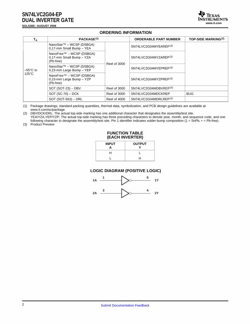
ORDERING INFORMATION
TA PACKAGE (1) ORDERABLE PART NUMBER TOP-SIDE MARKING (2)
NanoStar™ – WCSP (DSBGA) SN74LVC2G04MYEAREP (3)0,17-mm Small Bump – YEA
NanoFree™ – WCSP (DSBGA)0,17-mm Small Bump – YZA SN74LVC2G04MYZAREP (3)
(Pb-free)Reel of 3000
NanoStar™ – WCSP (DSBGA) SN74LVC2G04MYEPREP (3)–55°C to 0,23-mm Large Bump – YEP125°C NanoFree™ – WCSP (DSBGA)
0,23-mm Large Bump – YZP SN74LVC2G04MYZPREP (3)
(Pb-free)
SOT (SOT-23) – DBV Reel of 3000 SN74LVC2G04MDBVREP (3)
SOT (SC-70) – DCK Reel of 3000 SN74LVC2G04MDCKREP BUG
SOT (SOT-563) – DRL Reel of 4000 SN74LVC2G04MDRLREP (3)
(1) Package drawings, standard packing quantities, thermal data, symbolization, and PCB design guidelines are available atwww.ti.com/sc/package.
(2) DBV/DCK/DRL: The actual top-side marking has one additional character that designates the assembly/test site.YEA/YZA,YEP/YZP: The actual top-side marking has three preceding characters to denote year, month, and sequence code, and onefollowing character to designate the assembly/test site. Pin 1 identifier indicates solder-bump composition (1 = SnPb, • = Pb-free).
(3) Product Preview
FUNCTION TABLE(EACH INVERTER)
INPUT OUTPUTA Y
H L
L H
LOGIC DIAGRAM (POSITIVE LOGIC)
2 Submit Documentation Feedback

www.ti.com
Absolute Maximum Ratings (1)
SN74LVC2G04-EPDUAL INVERTER GATE
SGLS365–AUGUST 2006
over operating free-air temperature range (unless otherwise noted)
MIN MAX UNIT
VCC Supply voltage range –0.5 6.5 V
VI Input voltage range (2) –0.5 6.5 V
VO Voltage range applied to any output in the high-impedance or power-off state (2) –0.5 6.5 V
VO Voltage range applied to any output in the high or low state (2) (3) –0.5 VCC + 0.5 V
IIK Input clamp current VI < 0 –50 mA
IOK Output clamp current VO < 0 –50 mA
IO Continuous output current ±50 mA
Continuous current through VCC or GND ±100 mA
DBV package 165
DCK package 259
θJA Package thermal impedance (4) DRL package 142 °C/W
YEA/YZA package 143
YEP/YZP package 123
Tstg Storage temperature range –65 150 °C
(1) Stresses beyond those listed under "absolute maximum ratings" may cause permanent damage to the device. These are stress ratingsonly, and functional operation of the device at these or any other conditions beyond those indicated under "recommended operatingconditions" is not implied. Exposure to absolute-maximum-rated conditions for extended periods may affect device reliability.
(2) The input negative-voltage and output voltage ratings may be exceeded if the input and output current ratings are observed.(3) The value of VCC is provided in the recommended operating conditions table.(4) The package thermal impedance is calculated in accordance with JESD 51-7.
3Submit Documentation Feedback
www.ti.com
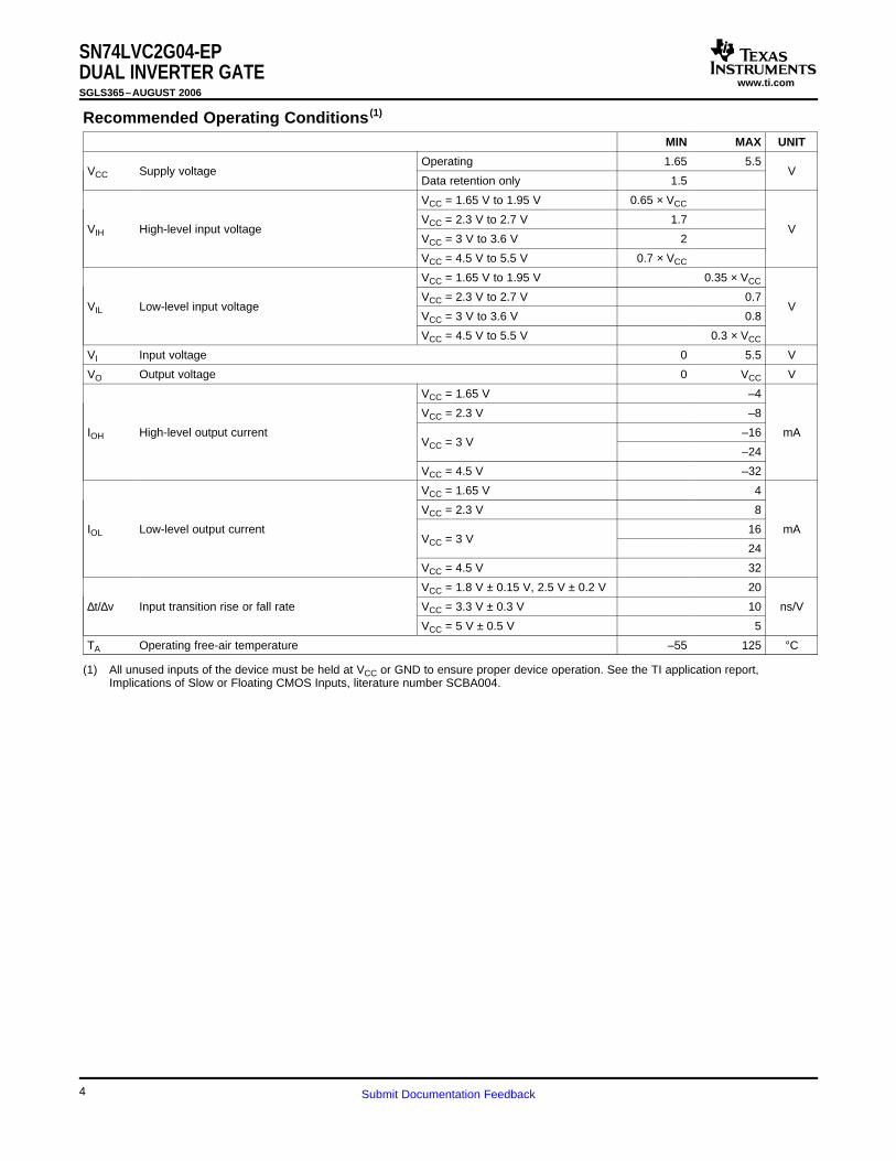
Recommended Operating Conditions (1)
SN74LVC2G04-EPDUAL INVERTER GATESGLS365–AUGUST 2006
MIN MAX UNIT
Operating 1.65 5.5VCC Supply voltage V
Data retention only 1.5
VCC = 1.65 V to 1.95 V 0.65 × VCC
VCC = 2.3 V to 2.7 V 1.7VIH High-level input voltage V
VCC = 3 V to 3.6 V 2
VCC = 4.5 V to 5.5 V 0.7 × VCC
VCC = 1.65 V to 1.95 V 0.35 × VCC
VCC = 2.3 V to 2.7 V 0.7VIL Low-level input voltage V
VCC = 3 V to 3.6 V 0.8
VCC = 4.5 V to 5.5 V 0.3 × VCC
VI Input voltage 0 5.5 V
VO Output voltage 0 VCC V
VCC = 1.65 V –4
VCC = 2.3 V –8
IOH High-level output current –16 mAVCC = 3 V
–24
VCC = 4.5 V –32
VCC = 1.65 V 4
VCC = 2.3 V 8
IOL Low-level output current 16 mAVCC = 3 V
24
VCC = 4.5 V 32
VCC = 1.8 V ± 0.15 V, 2.5 V ± 0.2 V 20
∆t/∆v Input transition rise or fall rate VCC = 3.3 V ± 0.3 V 10 ns/V
VCC = 5 V ± 0.5 V 5
TA Operating free-air temperature –55 125 °C
(1) All unused inputs of the device must be held at VCC or GND to ensure proper device operation. See the TI application report,Implications of Slow or Floating CMOS Inputs, literature number SCBA004.
4 Submit Documentation Feedback

www.ti.com
Electrical Characteristics
Switching Characteristics
Operating Characteristics
SN74LVC2G04-EPDUAL INVERTER GATE
SGLS365–AUGUST 2006
over recommended operating free-air temperature range (unless otherwise noted)
PARAMETER TEST CONDITIONS VCC MIN TYP (1) MAX UNIT
IOH = –100 µA 1.65 V to 5.5 V VCC – 0.1
IOH = –4 mA 1.65 V 1.2
IOH = –8 mA 2.3 V 1.9VOH V
IOH = –16 mA 2.43 V
IOH = –24 mA 2.3
IOH = –32 mA 4.5 V 3.8
IOL = 100 µA 1.65 V to 5.5 V 0.1
IOL = 4 mA 1.65 V 0.45
IOL = 8 mA 2.3 V 0.3VOL V
IOL = 16 mA 0.43 V
IOL = 24 mA 0.55
IOL = 32 mA 4.5 V 0.55
II A inputs VI = 5.5 V or GND 0 to 5.5 V ±5 µA
Ioff VI or VO = 5.5 V 0 ±10 µA
ICC VI = 5.5 V or GND, IO = 0 1.65 V to 5.5 V 10 µA
∆ICC One input at VCC – 0.6 V, Other inputs at VCC or GND 3 V to 5.5 V 500 µA
Ci VI = VCC or GND 3.3 V 3.5 pF
(1) All typical values are at VCC = 3.3 V, TA = 25°C.
over recommended operating free-air temperature range (unless otherwise noted) (see Figure 1)
VCC = 1.8 V VCC = 2.5 V VCC = 3.3 V VCC = 5 VFROM TO ± 0.15 V ± 0.2 V ± 0.3 V ± 0.5 VPARAMETER UNIT(INPUT) (OUTPUT)
MIN MAX MIN MAX MIN MAX MIN MAX
tpd A Y 3.1 8 1.5 6.0 1.2 5.0 1 4.0 ns
TA = 25°C
VCC = 1.8 V VCC = 2.5 V VCC = 3.3 V VCC = 5 VPARAMETER TEST CONDITIONS UNIT
TYP TYP TYP TYP
Cpd Power dissipation capacitance f = 10 MHz 14 14 14 16 pF
5Submit Documentation Feedback

www.ti.com
PARAMETER MEASUREMENT INFORMATION
VM
thtsu
From OutputUnder Test
CL(see Note A)
LOAD CIRCUIT
S1VLOAD
Open
GND
RL
RL
Data Input
Timing InputVI
0 V
VI
0 V0 V
tw
Input
VOLTAGE WAVEFORMSSETUP AND HOLD TIMES
VOLTAGE WAVEFORMSPROPAGATION DELAY TIMES
INVERTING AND NONINVERTING OUTPUTS
VOLTAGE WAVEFORMSPULSE DURATION
tPLH
tPHL
tPHL
tPLH
VOH
VOH
VOL
VOL
VI
0 VInput
OutputWaveform 1S1 at VLOAD(see Note B)
OutputWaveform 2
S1 at GND(see Note B)
VOL
VOH
tPZL
tPZH
tPLZ
tPHZ
VLOAD/2
0 V
VOL + V∆
VOH − V∆
≈0 V
VI
VOLTAGE WAVEFORMSENABLE AND DISABLE TIMES
LOW- AND HIGH-LEVEL ENABLING
Output
Output
tPLH/tPHLtPLZ/tPZLtPHZ/tPZH
OpenVLOADGND
TEST S1
NOTES: A. CL includes probe and jig capacitance.B. Waveform 1 is for an output with internal conditions such that the output is low, except when disabled by the output control.
Waveform 2 is for an output with internal conditions such that the output is high, except when disabled by the output control.C. All input pulses are supplied by generators having the following characteristics: PRR ≤ 10 MHz, ZO = 50 Ω.D. The outputs are measured one at a time, with one transition per measurement.E. tPLZ and tPHZ are the same as tdis.F. tPZL and tPZH are the same as ten.G. tPLH and tPHL are the same as tpd.H. All parameters and waveforms are not applicable to all devices.
OutputControl
VM VM
VM VM
VM VM
VM
VM VM
VM
VM
VM
VI
VM
VM
1.8 V ± 0.15 V2.5 V ± 0.2 V3.3 V ± 0.3 V5 V ± 0.5 V
1 kΩ500 Ω500 Ω500 Ω
VCC RL
2 × VCC2 × VCC
6 V2 × VCC
VLOAD CL
30 pF30 pF50 pF50 pF
0.15 V0.15 V0.3 V0.3 V
V∆
VCCVCC3 VVCC
VI
VCC/2VCC/21.5 VVCC/2
VMtr/tf
≤2 ns≤2 ns
≤2.5 ns≤2.5 ns
INPUTS
SN74LVC2G04-EPDUAL INVERTER GATESGLS365–AUGUST 2006
Figure 1. Load Circuit and Voltage Waveforms
6 Submit Documentation Feedback

PACKAGE OPTION ADDENDUM
www.ti.com 31-May-2014
Addendum-Page 1
PACKAGING INFORMATION
Orderable Device Status(1)
Package Type PackageDrawing
Pins PackageQty
Eco Plan(2)
Lead/Ball Finish(6)
MSL Peak Temp(3)
Op Temp (°C) Device Marking(4/5)
Samples
SN74LVC2G04MDCKREP ACTIVE SC70 DCK 6 3000 Green (RoHS& no Sb/Br)
CU NIPDAU Level-1-260C-UNLIM -55 to 125 BUG
V62/06632-01XE ACTIVE SC70 DCK 6 3000 Green (RoHS& no Sb/Br)
CU NIPDAU Level-1-260C-UNLIM -40 to 85 BUG
(1) The marketing status values are defined as follows:ACTIVE: Product device recommended for new designs.LIFEBUY: TI has announced that the device will be discontinued, and a lifetime-buy period is in effect.NRND: Not recommended for new designs. Device is in production to support existing customers, but TI does not recommend using this part in a new design.PREVIEW: Device has been announced but is not in production. Samples may or may not be available.OBSOLETE: TI has discontinued the production of the device.
(2) Eco Plan - The planned eco-friendly classification: Pb-Free (RoHS), Pb-Free (RoHS Exempt), or Green (RoHS & no Sb/Br) - please check http://www.ti.com/productcontent for the latest availabilityinformation and additional product content details.TBD: The Pb-Free/Green conversion plan has not been defined.Pb-Free (RoHS): TI's terms "Lead-Free" or "Pb-Free" mean semiconductor products that are compatible with the current RoHS requirements for all 6 substances, including the requirement thatlead not exceed 0.1% by weight in homogeneous materials. Where designed to be soldered at high temperatures, TI Pb-Free products are suitable for use in specified lead-free processes.Pb-Free (RoHS Exempt): This component has a RoHS exemption for either 1) lead-based flip-chip solder bumps used between the die and package, or 2) lead-based die adhesive used betweenthe die and leadframe. The component is otherwise considered Pb-Free (RoHS compatible) as defined above.Green (RoHS & no Sb/Br): TI defines "Green" to mean Pb-Free (RoHS compatible), and free of Bromine (Br) and Antimony (Sb) based flame retardants (Br or Sb do not exceed 0.1% by weightin homogeneous material)
(3) MSL, Peak Temp. - The Moisture Sensitivity Level rating according to the JEDEC industry standard classifications, and peak solder temperature.
(4) There may be additional marking, which relates to the logo, the lot trace code information, or the environmental category on the device.
(5) Multiple Device Markings will be inside parentheses. Only one Device Marking contained in parentheses and separated by a "~" will appear on a device. If a line is indented then it is a continuationof the previous line and the two combined represent the entire Device Marking for that device.
(6) Lead/Ball Finish - Orderable Devices may have multiple material finish options. Finish options are separated by a vertical ruled line. Lead/Ball Finish values may wrap to two lines if the finishvalue exceeds the maximum column width.
Important Information and Disclaimer:The information provided on this page represents TI's knowledge and belief as of the date that it is provided. TI bases its knowledge and belief on informationprovided by third parties, and makes no representation or warranty as to the accuracy of such information. Efforts are underway to better integrate information from third parties. TI has taken andcontinues to take reasonable steps to provide representative and accurate information but may not have conducted destructive testing or chemical analysis on incoming materials and chemicals.TI and TI suppliers consider certain information to be proprietary, and thus CAS numbers and other limited information may not be available for release.
PACKAGE OPTION ADDENDUM
www.ti.com 31-May-2014
Addendum-Page 2
In no event shall TI's liability arising out of such information exceed the total purchase price of the TI part(s) at issue in this document sold by TI to Customer on an annual basis.
OTHER QUALIFIED VERSIONS OF SN74LVC2G04-EP :
• Catalog: SN74LVC2G04
NOTE: Qualified Version Definitions:
• Catalog - TI's standard catalog product

TAPE AND REEL INFORMATION
*All dimensions are nominal
Device PackageType
PackageDrawing
Pins SPQ ReelDiameter
(mm)
ReelWidth
W1 (mm)
A0(mm)
B0(mm)
K0(mm)
P1(mm)
W(mm)
Pin1Quadrant
SN74LVC2G04MDCKREP SC70 DCK 6 3000 180.0 8.4 2.4 2.5 1.2 4.0 8.0 Q3
PACKAGE MATERIALS INFORMATION
www.ti.com 3-Aug-2017
Pack Materials-Page 1
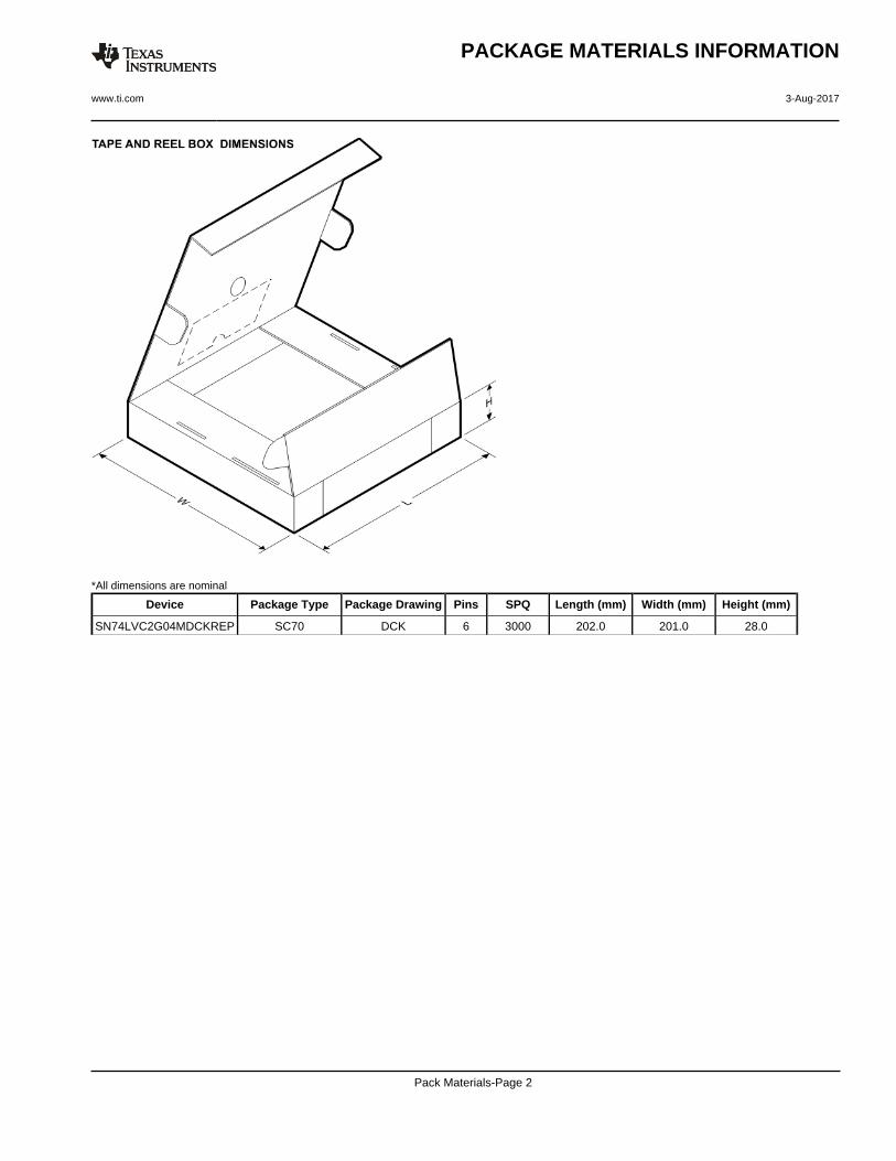
*All dimensions are nominal
Device Package Type Package Drawing Pins SPQ Length (mm) Width (mm) Height (mm)
SN74LVC2G04MDCKREP SC70 DCK 6 3000 202.0 201.0 28.0
PACKAGE MATERIALS INFORMATION
www.ti.com 3-Aug-2017
Pack Materials-Page 2


IMPORTANT NOTICE
Texas Instruments Incorporated (TI) reserves the right to make corrections, enhancements, improvements and other changes to itssemiconductor products and services per JESD46, latest issue, and to discontinue any product or service per JESD48, latest issue. Buyersshould obtain the latest relevant information before placing orders and should verify that such information is current and complete.TI’s published terms of sale for semiconductor products (http://www.ti.com/sc/docs/stdterms.htm) apply to the sale of packaged integratedcircuit products that TI has qualified and released to market. Additional terms may apply to the use or sale of other types of TI products andservices.Reproduction of significant portions of TI information in TI data sheets is permissible only if reproduction is without alteration and isaccompanied by all associated warranties, conditions, limitations, and notices. TI is not responsible or liable for such reproduceddocumentation. Information of third parties may be subject to additional restrictions. Resale of TI products or services with statementsdifferent from or beyond the parameters stated by TI for that product or service voids all express and any implied warranties for theassociated TI product or service and is an unfair and deceptive business practice. TI is not responsible or liable for any such statements.Buyers and others who are developing systems that incorporate TI products (collectively, “Designers”) understand and agree that Designersremain responsible for using their independent analysis, evaluation and judgment in designing their applications and that Designers havefull and exclusive responsibility to assure the safety of Designers' applications and compliance of their applications (and of all TI productsused in or for Designers’ applications) with all applicable regulations, laws and other applicable requirements. Designer represents that, withrespect to their applications, Designer has all the necessary expertise to create and implement safeguards that (1) anticipate dangerousconsequences of failures, (2) monitor failures and their consequences, and (3) lessen the likelihood of failures that might cause harm andtake appropriate actions. Designer agrees that prior to using or distributing any applications that include TI products, Designer willthoroughly test such applications and the functionality of such TI products as used in such applications.TI’s provision of technical, application or other design advice, quality characterization, reliability data or other services or information,including, but not limited to, reference designs and materials relating to evaluation modules, (collectively, “TI Resources”) are intended toassist designers who are developing applications that incorporate TI products; by downloading, accessing or using TI Resources in anyway, Designer (individually or, if Designer is acting on behalf of a company, Designer’s company) agrees to use any particular TI Resourcesolely for this purpose and subject to the terms of this Notice.TI’s provision of TI Resources does not expand or otherwise alter TI’s applicable published warranties or warranty disclaimers for TIproducts, and no additional obligations or liabilities arise from TI providing such TI Resources. TI reserves the right to make corrections,enhancements, improvements and other changes to its TI Resources. TI has not conducted any testing other than that specificallydescribed in the published documentation for a particular TI Resource.Designer is authorized to use, copy and modify any individual TI Resource only in connection with the development of applications thatinclude the TI product(s) identified in such TI Resource. NO OTHER LICENSE, EXPRESS OR IMPLIED, BY ESTOPPEL OR OTHERWISETO ANY OTHER TI INTELLECTUAL PROPERTY RIGHT, AND NO LICENSE TO ANY TECHNOLOGY OR INTELLECTUAL PROPERTYRIGHT OF TI OR ANY THIRD PARTY IS GRANTED HEREIN, including but not limited to any patent right, copyright, mask work right, orother intellectual property right relating to any combination, machine, or process in which TI products or services are used. Informationregarding or referencing third-party products or services does not constitute a license to use such products or services, or a warranty orendorsement thereof. Use of TI Resources may require a license from a third party under the patents or other intellectual property of thethird party, or a license from TI under the patents or other intellectual property of TI.TI RESOURCES ARE PROVIDED “AS IS” AND WITH ALL FAULTS. TI DISCLAIMS ALL OTHER WARRANTIES ORREPRESENTATIONS, EXPRESS OR IMPLIED, REGARDING RESOURCES OR USE THEREOF, INCLUDING BUT NOT LIMITED TOACCURACY OR COMPLETENESS, TITLE, ANY EPIDEMIC FAILURE WARRANTY AND ANY IMPLIED WARRANTIES OFMERCHANTABILITY, FITNESS FOR A PARTICULAR PURPOSE, AND NON-INFRINGEMENT OF ANY THIRD PARTY INTELLECTUALPROPERTY RIGHTS. TI SHALL NOT BE LIABLE FOR AND SHALL NOT DEFEND OR INDEMNIFY DESIGNER AGAINST ANY CLAIM,INCLUDING BUT NOT LIMITED TO ANY INFRINGEMENT CLAIM THAT RELATES TO OR IS BASED ON ANY COMBINATION OFPRODUCTS EVEN IF DESCRIBED IN TI RESOURCES OR OTHERWISE. IN NO EVENT SHALL TI BE LIABLE FOR ANY ACTUAL,DIRECT, SPECIAL, COLLATERAL, INDIRECT, PUNITIVE, INCIDENTAL, CONSEQUENTIAL OR EXEMPLARY DAMAGES INCONNECTION WITH OR ARISING OUT OF TI RESOURCES OR USE THEREOF, AND REGARDLESS OF WHETHER TI HAS BEENADVISED OF THE POSSIBILITY OF SUCH DAMAGES.Unless TI has explicitly designated an individual product as meeting the requirements of a particular industry standard (e.g., ISO/TS 16949and ISO 26262), TI is not responsible for any failure to meet such industry standard requirements.Where TI specifically promotes products as facilitating functional safety or as compliant with industry functional safety standards, suchproducts are intended to help enable customers to design and create their own applications that meet applicable functional safety standardsand requirements. Using products in an application does not by itself establish any safety features in the application. Designers mustensure compliance with safety-related requirements and standards applicable to their applications. Designer may not use any TI products inlife-critical medical equipment unless authorized officers of the parties have executed a special contract specifically governing such use.Life-critical medical equipment is medical equipment where failure of such equipment would cause serious bodily injury or death (e.g., lifesupport, pacemakers, defibrillators, heart pumps, neurostimulators, and implantables). Such equipment includes, without limitation, allmedical devices identified by the U.S. Food and Drug Administration as Class III devices and equivalent classifications outside the U.S.TI may expressly designate certain products as completing a particular qualification (e.g., Q100, Military Grade, or Enhanced Product).Designers agree that it has the necessary expertise to select the product with the appropriate qualification designation for their applicationsand that proper product selection is at Designers’ own risk. Designers are solely responsible for compliance with all legal and regulatoryrequirements in connection with such selection.Designer will fully indemnify TI and its representatives against any damages, costs, losses, and/or liabilities arising out of Designer’s non-compliance with the terms and provisions of this Notice.
Mailing Address: Texas Instruments, Post Office Box 655303, Dallas, Texas 75265Copyright © 2017, Texas Instruments Incorporated