
Slide 1 QCS Confidential Version 1.0 SCP Models QCS Introduction SCP Technology ROST TM Technology...
54
Slide 1 QCS Confidential Version 1.0 SCP Models QCS Introduction SCP Technology ROST TM Technology Performance Examples Reliability Summary QC Solutions, Inc. QC Solutions, Inc. QCS Metrology Overview QCS Metrology Overview Surface Charge Profiler Surface Charge Profiler QCS-7000 Series QCS-7000 Series
-
Upload
eugene-stewart -
Category
Documents
-
view
219 -
download
3
Transcript of Slide 1 QCS Confidential Version 1.0 SCP Models QCS Introduction SCP Technology ROST TM Technology...

Slide 1
QCS Confidential Version 1.0
SCP Models
QCS Introduction
SCP Technology
ROSTTM Technology
Performance
Examples
Reliability
Summary
QC Solutions, Inc.QC Solutions, Inc.
QCS Metrology Overview QCS Metrology Overview Surface Charge Profiler Surface Charge Profiler
QCS-7000 SeriesQCS-7000 Series
Slide 2
QCS Confidential Version 1.0
SCP Models
QCS Introduction
SCP Technology
ROSTTM Technology
Performance
Examples
Reliability
Summary
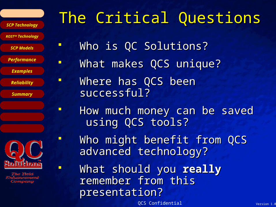
The Critical QuestionsThe Critical Questions
Who is QC Solutions?Who is QC Solutions?
What makes QCS unique?What makes QCS unique?
Where has QCS been successful?Where has QCS been successful?
How much money can be saved How much money can be saved using QCS tools?using QCS tools?
Who might benefit from QCS Who might benefit from QCS advanced technology?advanced technology?
What should you What should you reallyreally remember remember from this presentation?from this presentation?

Slide 3
QCS Confidential Version 1.0
SCP Models
QCS Introduction
SCP Technology
ROSTTM Technology
Performance
Examples
Reliability
Summary
QC Solutions – The CompanyQC Solutions – The Company
Founded in 1993 as R&D by Dr. Emil Kamieniecki to investigate Founded in 1993 as R&D by Dr. Emil Kamieniecki to investigate methods for non-contact surface charge monitoringmethods for non-contact surface charge monitoring
1997 introduction of ROST™ technology and shipment of first 1997 introduction of ROST™ technology and shipment of first commercial product for metrology of epitaxial layers (QCS-7000 commercial product for metrology of epitaxial layers (QCS-7000 series)series)
1999 relocation to larger facility in Billerica, MA including clean 1999 relocation to larger facility in Billerica, MA including clean room application center and manufacturingroom application center and manufacturing
By 2000, the QCS-7000 series has been accepted and is being By 2000, the QCS-7000 series has been accepted and is being used by more than 85% of the large volume wafer manufacturers.used by more than 85% of the large volume wafer manufacturers.
In Q1-2002 QC Solutions will expand into the ion implantation In Q1-2002 QC Solutions will expand into the ion implantation market utilizing its highly sensitive technology for low dose ion market utilizing its highly sensitive technology for low dose ion implant measurement.implant measurement.

Slide 4
QCS Confidential Version 1.0
SCP Models
QCS Introduction
SCP Technology
ROSTTM Technology
Performance
Examples
Reliability
Summary
What makes QCS unique?What makes QCS unique?
The answer is: The answer is:
The application of our patented The application of our patented technologies!technologies!
The SCP measurement The SCP measurement principleprinciple
In-Situ surface conditioningIn-Situ surface conditioning

Slide 5
QCS Confidential Version 1.0
SCP Models
QCS Introduction
SCP Technology
ROSTTM Technology
Performance
Examples
Reliability
Summary
SCP Principle of Operation SCP Principle of Operation
LIGHT SOURCE
SU
RF
AC
ED
EP
LE
TIO
N
LA
YE
R
P-TYPE Si BULK (NEUTRAL)
MODULATED BEAM OF COLLIMATED LIGHT[h > EG(Si)]
LIG
HT
PE
NE
TR
AT
ION
RE
GIO
N
+ + + + - + + + + + + - 100 m
COUNTER-ELECTRODE
Vs
EL
EC
TR
IC F
IEL
D
e
h
e
he
h
e
h
e
h
e
h
e
h~ 1 m

Slide 6
QCS Confidential Version 1.0
SCP Models
QCS Introduction
SCP Technology
ROSTTM Technology
Performance
Examples
Reliability
Summary
Where has QCS been Where has QCS been successful so far?successful so far?
The answer is: The answer is:
In the Silicon Epitaxy Market In the Silicon Epitaxy Market where 85% of the large wafer where 85% of the large wafer manufacturers have accepted manufacturers have accepted and are using this technology.and are using this technology.
Slide 7
QCS Confidential Version 1.0
SCP Models
QCS Introduction
SCP Technology
ROSTTM Technology
Performance
Examples
Reliability
Summary
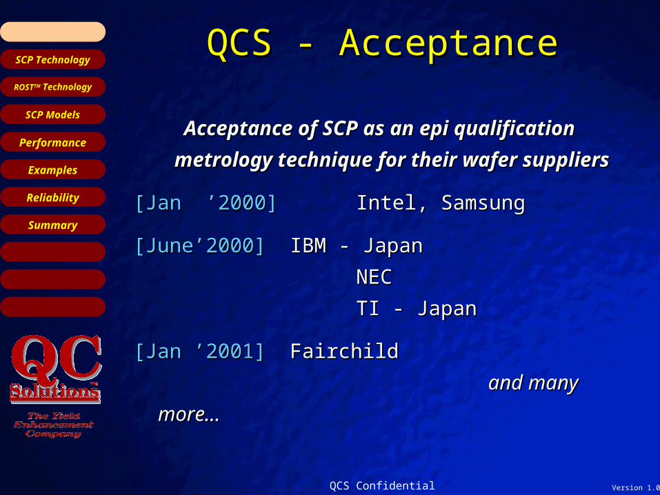
QCS - AcceptanceQCS - Acceptance
Acceptance of SCP as an epi qualification Acceptance of SCP as an epi qualification
metrology technique for their wafer suppliersmetrology technique for their wafer suppliers
[Jan ’2000] [Jan ’2000] Intel, SamsungIntel, Samsung
[June’2000] [June’2000] IBM - JapanIBM - Japan
NECNEC
TI - JapanTI - Japan
[Jan ’2001] [Jan ’2001] FairchildFairchild
and many more…and many more…

Slide 8
QCS Confidential Version 1.0
SCP Models
QCS Introduction
SCP Technology
ROSTTM Technology
Performance
Examples
Reliability
Summary
How much money can be How much money can be saved using QCS tools?saved using QCS tools?
The answer is: The answer is:
Savings that are directly related to Savings that are directly related to reduced monitor wafer usage.reduced monitor wafer usage.
Savings attributed to preservation of Savings attributed to preservation of funds due to incident avoidance. funds due to incident avoidance.
Both can add up to much more than Both can add up to much more than you think!you think!
Slide 9
QCS Confidential Version 1.0
SCP Models
QCS Introduction
SCP Technology
ROSTTM Technology
Performance
Examples
Reliability
Summary
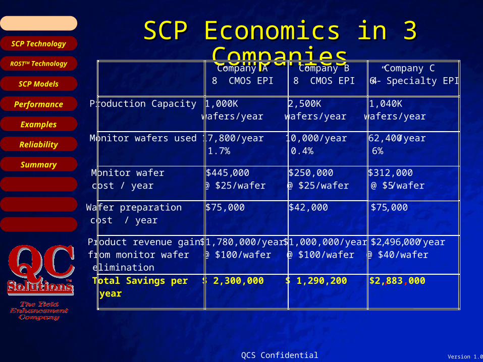
SCP Economics in 3 CompaniesSCP Economics in 3 Companies
Company A 8” CMOS EPI
Company B 8” CMOS EPI
Company C 4-6” Specialty EPI
Production Capacity 1,000K wafers/year
2,500K wafers/year
1,040K wafers/year
Monitor wafers used 17,800/year 1.7%
10,000/year 0.4%
62,400 /year 6%
Monitor wafer cost / year
$445, 000 @ $25/wafer
$250,000 @ $25/wafer
$312,000 @ $5 /wafer
Wafer preparation cost / year
$75,000 $42,000 $75,000
Product revenue gain from monitor wafer elimination
$1,780,000/year @ $100/wafer
$1,000,000/year @ $100/wafer
$2,496,000/year @ $40/wafer
Total Savings peryear
$ 2,300,000 $ 1,290,200 $ 2,883,000, ,

Slide 10
QCS Confidential Version 1.0
SCP Models
QCS Introduction
SCP Technology
ROSTTM Technology
Performance
Examples
Reliability
Summary
Cost of Real Wafer Quality Cost of Real Wafer Quality Incident in Device FabIncident in Device Fab11
33% of epi wafer shipments (more than 1500 33% of epi wafer shipments (more than 1500 wafers) were out-of-spec at the surface, resulting wafers) were out-of-spec at the surface, resulting in 33% yield reduction (0% yield on 1/3 of wafers)in 33% yield reduction (0% yield on 1/3 of wafers)
The SCP tool caught the problem while doing a The SCP tool caught the problem while doing a process evaluation process evaluation
The wafer manufacturer used Hg-CV for outgoing The wafer manufacturer used Hg-CV for outgoing quality control and did not see the problemquality control and did not see the problem
How much money did QCS save this customer on How much money did QCS save this customer on this ONE incident?this ONE incident?
1 Source: Fairchild Semiconductor, Inc. “Benefits of Non-destructive Resistivity Testing in Silicon Epitaxial Wafer Quality Control” Semicon West 2000 Silicon Symposium

Slide 11
QCS Confidential Version 1.0
SCP Models
QCS Introduction
SCP Technology
ROSTTM Technology
Performance
Examples
Reliability
Summary
$$ Saved Dollars $$$$ Saved Dollars $$
““Wafer Cost” = $160,000Wafer Cost” = $160,000(includes material, fab processing, and test)(includes material, fab processing, and test)
Packaging Cost = $160,000Packaging Cost = $160,000(wafers could be screened at fab)(wafers could be screened at fab)
Opportunity Cost = $270,000Opportunity Cost = $270,000(gross profit margin lost)(gross profit margin lost)
In Total: $590,000In Total: $590,000
Slide 12
QCS Confidential Version 1.0
SCP Models
QCS Introduction
SCP Technology
ROSTTM Technology
Performance
Examples
Reliability
Summary
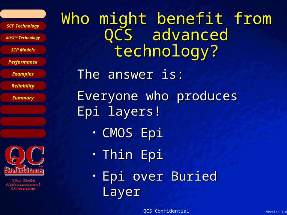
Who might benefit from QCS Who might benefit from QCS advanced technology?advanced technology?
The answer is: The answer is:
Everyone who produces Epi Everyone who produces Epi layers!layers!
• CMOS EpiCMOS Epi
• Thin EpiThin Epi
• Epi over Buried LayerEpi over Buried Layer

Slide 13
QCS Confidential Version 1.0
SCP Models
QCS Introduction
SCP Technology
ROSTTM Technology
Performance
Examples
Reliability
Summary
What should you What should you reallyreally remember about QC Solutions?remember about QC Solutions?
The answer is:
Superior technology
Reliable, field proven hardware
Attractive ROI through cost savings/cost avoidance

Slide 14
QCS Confidential Version 1.0
SCP Models
QCS Introduction
SCP Technology
ROSTTM Technology
Performance
Examples
Reliability
Summary
Principles of OperationPrinciples of Operation

Slide 15
QCS Confidential Version 1.0
SCP Models
QCS Introduction
SCP Technology
ROSTTM Technology
Performance
Examples
Reliability
Summary
SCP Principles of Operation SCP Principles of Operation
LIGHT SOURCE
SU
RF
AC
ED
EP
LE
TIO
N
LA
YE
R
P-TYPE Si BULK (NEUTRAL)
MODULATED BEAM OF COLLIMATED LIGHT[h > EG(Si)]
LIG
HT
PE
NE
TR
AT
ION
RE
GIO
N
+ + + + - + + + + + + - 100 m
COUNTER-ELECTRODE
Vs
EL
EC
TR
IC F
IEL
D
e
h
e
he
h
e
h
e
h
e
h
e
h~ 1 m

Slide 16
QCS Confidential Version 1.0
SCP Models
QCS Introduction
SCP Technology
ROSTTM Technology
Performance
Examples
Reliability
Summary
SCP Block DiagramSCP Block Diagram
WAFER SUPPORT WITH INSULATING COATING
SIGNALPROCESSING
MOTIONCONTROLLER
PROBE MOTION CONTROL
SYSTEM CONTROL STATION
WAFER
LEDLIGHT SOURCE
DATA ACQUISITION
ELECTRICAL & OPTICAL CABLES
WAFER MOTION
NON-
CONTACT
PROBE

Slide 17
QCS Confidential Version 1.0
SCP Models
QCS Introduction
SCP Technology
ROSTTM Technology
Performance
Examples
Reliability
Summary
Surface Charge ProfileSurface Charge ProfileSPV Measured Surface CapacitanceSPV Measured Surface Capacitance
• High frequency surface photo voltage
• Low intensity: Vs < 0.05 kT/q
• Peak wavelength 450 nm
• Light penetration depth < 0.4 m
Vs Wd Cs
Wd-inv = ƒ(Nsc)
• No change of net wafer charge
( QWFR = 0)
• No external current flow
Illumination
~~~~
Wd
Vs Wd
h
e
h
Re
Rh
Dark
Bulkp-type
h
0Q +
-
Slide 18
QCS Confidential Version 1.0
SCP Models
QCS Introduction
SCP Technology
ROSTTM Technology
Performance
Examples
Reliability
Summary
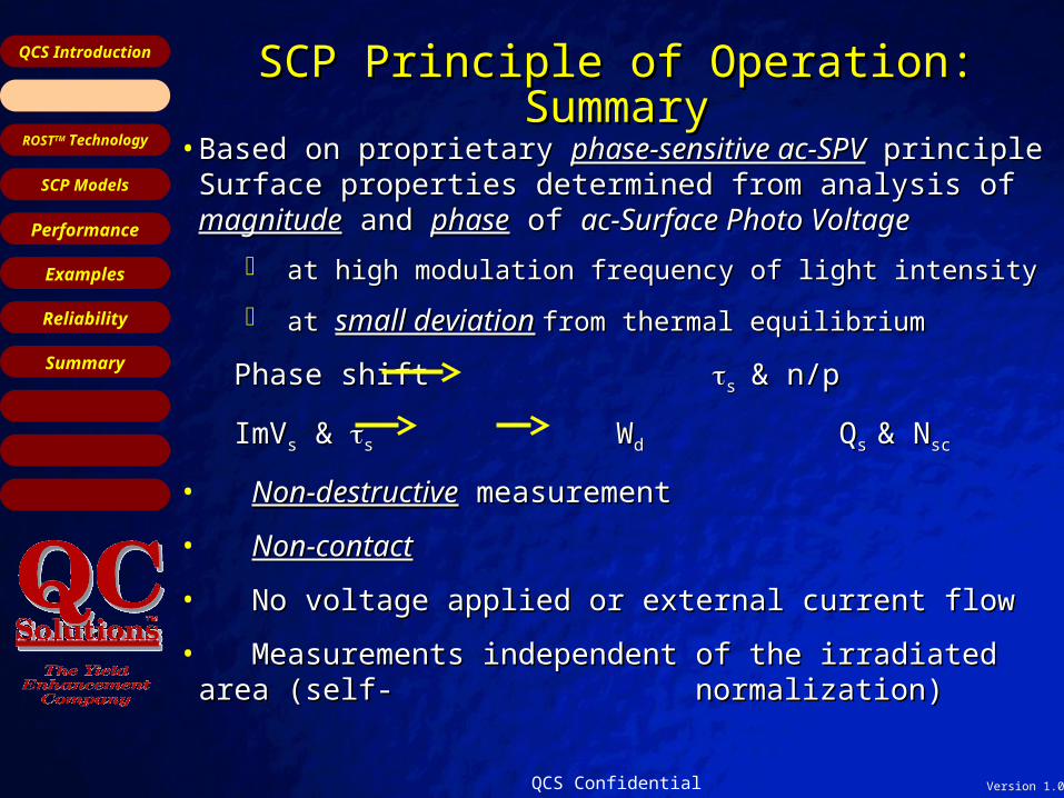
SCP Principle of Operation: SummarySCP Principle of Operation: Summary
• Based on proprietary Based on proprietary phase-sensitive ac-SPVphase-sensitive ac-SPV principle principleSurface properties determined from analysis of Surface properties determined from analysis of magnitudemagnitude and and phasephase of of ac-Surface Photo Voltageac-Surface Photo Voltage
at high modulation frequency of light intensityat high modulation frequency of light intensity
at at small deviationsmall deviation from thermal equilibriumfrom thermal equilibrium
Phase shift Phase shift ss&& n/pn/p
ImVImVss && ss WWdd QQs s & N& Nscsc
• Non-destructiveNon-destructive measurement measurement
• Non-contactNon-contact
• No voltage applied or external current flowNo voltage applied or external current flow
• Measurements independent of the irradiated area (self- Measurements independent of the irradiated area (self- normalization)normalization)
Slide 19
QCS Confidential Version 1.0
SCP Models
QCS Introduction
SCP Technology
ROSTTM Technology
Performance
Examples
Reliability
Summary
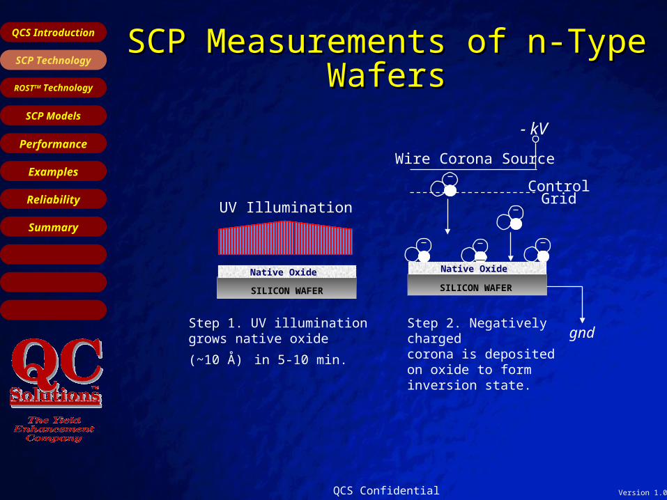
SCP Measurements of n-Type SCP Measurements of n-Type WafersWafers
- kV
SILICON WAFER
gnd
Wire Corona Source
ControlGrid
Native Oxide
UV Illumination
SILICON WAFER
Native Oxide
Step 1. UV illuminationgrows native oxide
(~10 Å) in 5-10 min.
Step 2. Negatively chargedcorona is deposited on oxide to forminversion state.

Slide 20
QCS Confidential Version 1.0
SCP Models
QCS Introduction
SCP Technology
ROSTTM Technology
Performance
Examples
Reliability
Summary
SCP Measurements of n-Type SCP Measurements of n-Type WafersWafers
0.0
0.1
0.2
0.3
0.4
0.5
0.6
Corona Charge Applied
Dep
leti
on
Wid
th (
mic
ron
s)
0.00
0.02
0.04
0.06
0.08
0.10
0.12
0.14
0.16
Inve
rse
Lif
etim
e (u
sec^
-1)
Depletion Width Inverse Lifetime
Wmax = 0.57 um
(2.5E+15/cm^3)

Slide 21
QCS Confidential Version 1.0
SCP Models
QCS Introduction
SCP Technology
ROSTTM Technology
Performance
Examples
Reliability
Summary
Determination of Doping ConcentrationDetermination of Doping Concentrationfrom Maximum Depletion Layer Widthfrom Maximum Depletion Layer Width
0.01
0.1
1
10
100
1E+12 1E+13 1E+14 1E+15 1E+16 1E+17 1E+18 1E+19
Nsc (cm3)
Wd
(m
icro
ns
)

Slide 22
QCS Confidential Version 1.0
SCP Models
QCS Introduction
SCP Technology
ROSTTM Technology
Performance
Examples
Reliability
Summary
ROST™ Principles of OperationROST™ Principles of Operation

Slide 23
QCS Confidential Version 1.0
SCP Models
QCS Introduction
SCP Technology
ROSTTM Technology
Performance
Examples
Reliability
Summary
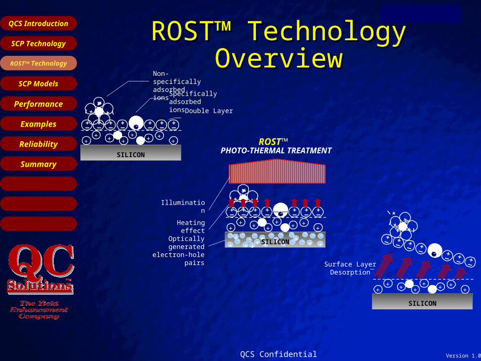
ROST™ Technology OverviewROST™ Technology Overview
++ + +
+ + ++
--
SILICON
Start with ANY Oxide Layer
++ + +
+ + ++
-
--
+_
+_+_ +_
+_
+_
+_+_ + _
+_
+_+_-
SILICON
Formation of theDouble Layer
++ + +
+ + ++
--
-
+_ +_ +_ +_ +_ +_ +_
+_ + _
+_
+_+_-
SILICON
Specifically adsorbed ions
Non-specifically adsorbed ions
DoubleLayer
Double Layer
Slide 24
QCS Confidential Version 1.0
SCP Models
QCS Introduction
SCP Technology
ROSTTM Technology
Performance
Examples
Reliability
Summary
PHOTO-THERMAL TREATMENTROST™
++ + +
+ + ++
--
+
- - - - - - - -
+ ++
++
+- - --
-+
+++
+SILICON
-+_ +_ +_ +_ +_ +_ +_
+_ + _
+_
+_+_-
Heating effect
Optically generated electron-hole pairs
Illumination
ROST™ Technology OverviewROST™ Technology Overview
++ + +
+ + ++
--
SILICON
-
+_ +_ +_ +_+_ +_ +_
+_ + _
+_+_
+_-
Surface LayerDesorption
++ + +
+ + ++
--
-
+_ +_ +_ +_ +_ +_ +_
+_ + _
+_
+_+_-
SILICON
Specifically adsorbed ions
Non-specifically adsorbed ions
Double Layer

Slide 25
QCS Confidential Version 1.0
SCP Models
QCS Introduction
SCP Technology
ROSTTM Technology
Performance
Examples
Reliability
Summary
ROST™ Processing ChamberROST™ Processing Chamber
INFRARED SENSOR
WAFER
LAMP POWERCONTROLLER
ILLUMINATION (<30sec)
PROPRIATORY
OPTICAL
FILTER

Slide 26
QCS Confidential Version 1.0
SCP Models
QCS Introduction
SCP Technology
ROSTTM Technology
Performance
Examples
Reliability
Summary
SCP ModelsSCP Models
Slide 27
QCS Confidential Version 1.0
SCP Models
QCS Introduction
SCP Technology
ROSTTM Technology
Performance
Examples
Reliability
Summary
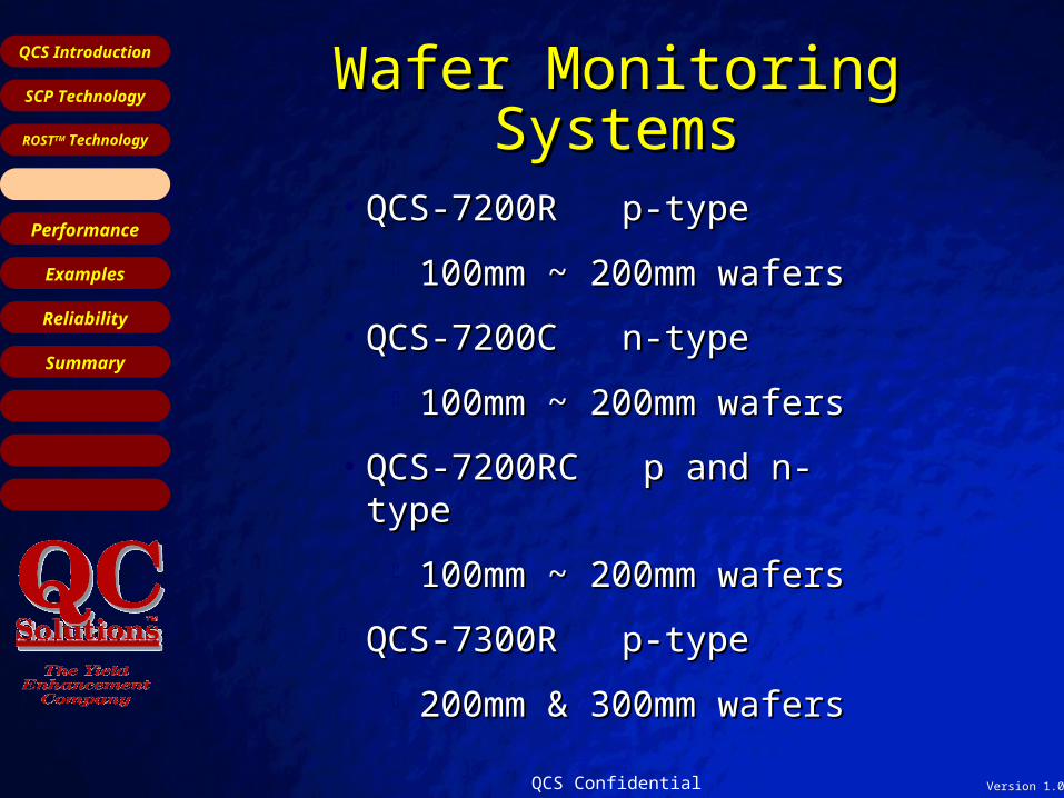
Wafer Monitoring SystemsWafer Monitoring Systems
• QCS-7200R p-type QCS-7200R p-type
100mm ~ 200mm wafers100mm ~ 200mm wafers
• QCS-7200C n-typeQCS-7200C n-type
100mm ~ 200mm wafers100mm ~ 200mm wafers
• QCS-7200RC p and n-type QCS-7200RC p and n-type
100mm ~ 200mm wafers100mm ~ 200mm wafers
QCS-7300R p-typeQCS-7300R p-type
200mm & 300mm wafers200mm & 300mm wafers
Slide 28
QCS Confidential Version 1.0
SCP Models
QCS Introduction
SCP Technology
ROSTTM Technology
Performance
Examples
Reliability
Summary
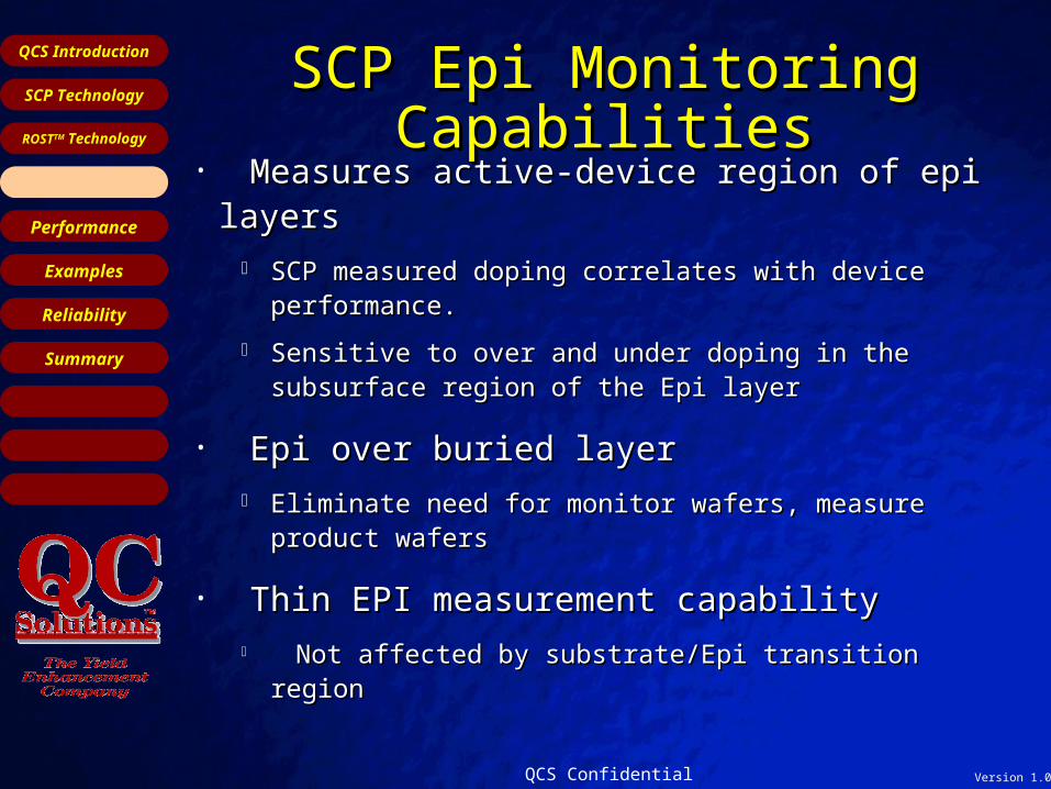
SCP Epi Monitoring CapabilitiesSCP Epi Monitoring Capabilities
• Measures active-device region of epi layersMeasures active-device region of epi layers SCP measured doping correlates with device SCP measured doping correlates with device
performance. performance.
Sensitive to over and under doping in the subsurface Sensitive to over and under doping in the subsurface region of the Epi layerregion of the Epi layer
• Epi over buried layerEpi over buried layer Eliminate need for monitor wafers, measure product Eliminate need for monitor wafers, measure product
waferswafers
• Thin EPI measurement capabilityThin EPI measurement capability Not affected by substrate/Epi transition regionNot affected by substrate/Epi transition region

Slide 29
QCS Confidential Version 1.0
SCP Models
QCS Introduction
SCP Technology
ROSTTM Technology
Performance
Examples
Reliability
Summary
Measurement ParametersMeasurement Parameters
QCS-7000 Series tool provides various QCS-7000 Series tool provides various measurements, here is a list of some of measurements, here is a list of some of the most often usedthe most often used NNscsc - Doping Concentration - Doping Concentration ResRes - Resistivity (Ohms-cm)- Resistivity (Ohms-cm)
QQss - Surface Charge- Surface Charge
WWdd - Depletion Layer Width (u- Depletion Layer Width (um) 1/t1/t - Surface Recombination Lifetime- Surface Recombination Lifetime p/np/n - Conductivity type- Conductivity type

Slide 30
QCS Confidential Version 1.0
SCP Models
QCS Introduction
SCP Technology
ROSTTM Technology
Performance
Examples
Reliability
Summary
SCP SpecificationsSCP Specifications
• Resistivity Repeatability with production wafers:Resistivity Repeatability with production wafers: p-type:p-type: 1%, 1 sigma <0.1 - >500 ohm-cm1%, 1 sigma <0.1 - >500 ohm-cm
n-type:n-type: 1%, 1 sigma <0.1 - 15 ohm-cm1%, 1 sigma <0.1 - 15 ohm-cm
1.5%, 1 sigma 15 - 30 ohm-cm1.5%, 1 sigma 15 - 30 ohm-cm
2%, 1 sigma 30 - 50 ohm-cm2%, 1 sigma 30 - 50 ohm-cm
• Surface Recombination Lifetime Surface Recombination Lifetime 0.5 - 1000 0.5 - 1000 secsec
• Throughput *Throughput * ~ 30 wph (p-type)~ 30 wph (p-type)
• Wafer SizesWafer Sizes 100 mm ~ 200 mm or 100 mm ~ 200 mm or
200 mm - 300 mm200 mm - 300 mm* Measurement resolution and wafer type dependant* Measurement resolution and wafer type dependant

Slide 31
QCS Confidential Version 1.0
SCP Models
QCS Introduction
SCP Technology
ROSTTM Technology
Performance
Examples
Reliability
Summary
SCP ApplicationsSCP Applications
• Epi Wafer ManufacturingEpi Wafer Manufacturing
• Process monitoring of production wafersProcess monitoring of production wafers
• Process development / tool qualificationProcess development / tool qualification
• Specialty EpiSpecialty Epi
• Incoming inspection Incoming inspection
• Process development / tool qualificationProcess development / tool qualification
• In-line monitoring of product wafersIn-line monitoring of product wafers
• Ion ImplantationIon Implantation
• Implant monitoringImplant monitoring

Slide 32
QCS Confidential Version 1.0
SCP Models
QCS Introduction
SCP Technology
ROSTTM Technology
Performance
Examples
Reliability
Summary
SCP PerformanceSCP Performance
Slide 33
QCS Confidential Version 1.0
SCP Models
QCS Introduction
SCP Technology
ROSTTM Technology
Performance
Examples
Reliability
Summary
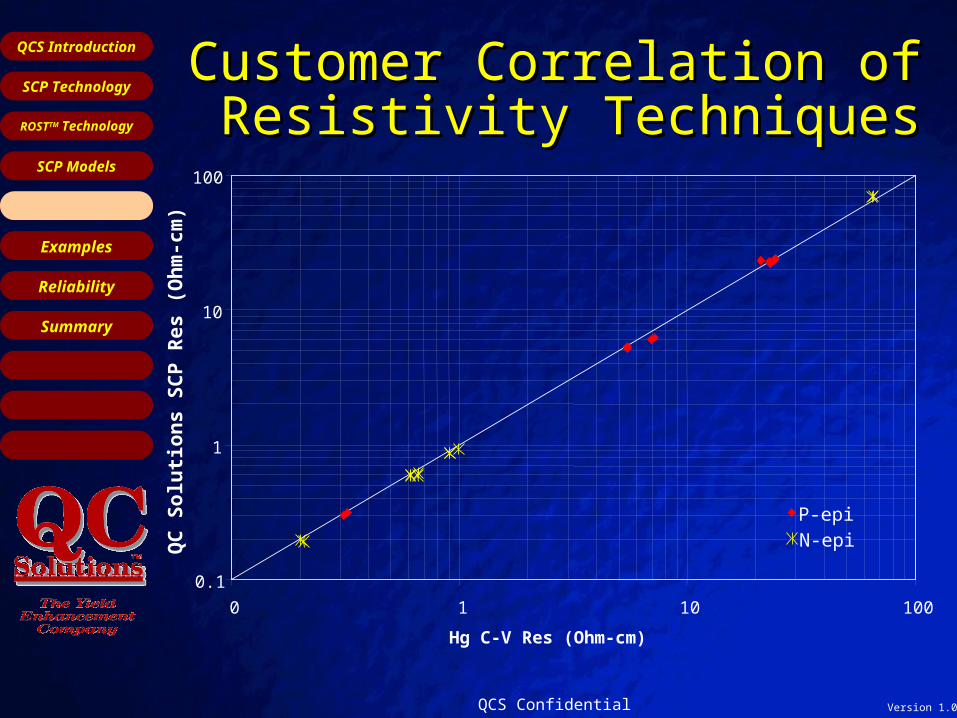
Customer Correlation ofCustomer Correlation of Resistivity Techniques Resistivity Techniques
QC
So
luti
on
s S
CP
Re
s (
Oh
m-c
m)
0.1
1
10
100
0 1 10 100
Hg C-V Res (Ohm-cm)
P-epiN-epi
Slide 34
QCS Confidential Version 1.0
SCP Models
QCS Introduction
SCP Technology
ROSTTM Technology
Performance
Examples
Reliability
Summary
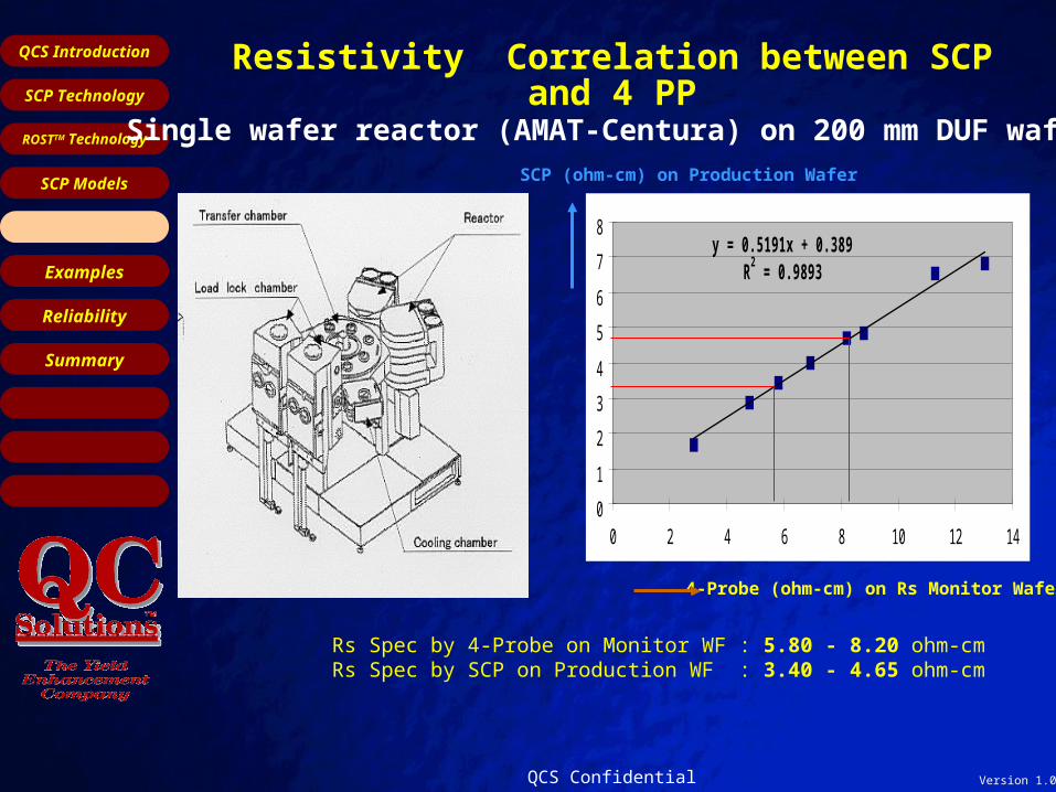
Resistivity Correlation between SCP and 4 PP
y = 0. 5191x + 0. 389R2 = 0. 9893
0
1
2
3
4
5
6
7
8
0 2 4 6 8 10 12 14
SCP (ohm-cm) on Production Wafer
4-Probe (ohm-cm) on Rs Monitor Wafer
Rs Spec by 4-Probe on Monitor WF : 5.80 - 8.20 ohm-cmRs Spec by SCP on Production WF : 3.40 - 4.65 ohm-cm
Single wafer reactor (AMAT-Centura) on 200 mm DUF wafer

Slide 35
QCS Confidential Version 1.0
SCP Models
QCS Introduction
SCP Technology
ROSTTM Technology
Performance
Examples
Reliability
Summary
Resistivity Correlation between SCP and 4 PP
Rsh monitor waferRsh monitor wafer will move from Top to will move from Top to Bottom by Epi Run Bottom by Epi Run circulatorycirculatory
Productionwafer
Monitor Waferfor 4-Probe
TopMiddleBottom
SCP (ohm-cm) on Production Wafer
4-Probe (ohm-cm) on Rs Monitor Wafer
y = 0.4314x + 0.1788R2 = 0.9999
0
1
2
3
4
5
6
0 1 2 3 4 5 6 7 8 9 10 11 12
Rs Spec by 4-Probe on Monitor WF : 5.80 - 8.20 ohm-cmRs Spec by SCP on Production WF : 2.68 - 3.72 ohm-cm
Batch type reactor (PE-7700) on 150 mm DUF wafer

Slide 36
QCS Confidential Version 1.0
SCP Models
QCS Introduction
SCP Technology
ROSTTM Technology
Performance
Examples
Reliability
Summary
SCP Spatial Resolution TestSCP Spatial Resolution Test
Wd
(um
)
0.0
0.1
0.2
0.3
0.4
0.5
0.6
0.7
0.8
-10 -8 -6 -4 -2 0 2 4 6 8 10
Position along x diameter
Point PatternMedium Resolution Map Delta x = 0.4mmHigh Resolution Map Delta x = 0.25mm
2 mm
4 mm
N-typeSubstrate
Boron diffusedinto N-typeSubstrate

Slide 37
QCS Confidential Version 1.0
SCP Models
QCS Introduction
SCP Technology
ROSTTM Technology
Performance
Examples
Reliability
Summary Examples of SCP Examples of SCP MeasurementMeasurement

Slide 38
QCS Confidential Version 1.0
SCP Models
QCS Introduction
SCP Technology
ROSTTM Technology
Performance
Examples
Reliability
Summary
Epi Reactor QualificationEpi Reactor Qualification
Maps show depletion width of as-received wafers, measured by SCP 7200. Wafers are 200mm diameter
p-type.
Comparison of Silicon Epi Reactors
Reactor A Reactor B

Slide 39
QCS Confidential Version 1.0
SCP Models
QCS Introduction
SCP Technology
ROSTTM Technology
Performance
Examples
Reliability
Summary
SUMITOMO METAL EPITECH ( EUROPE )
There are 3 wafers (points) measured per Epi run
SCP detected process anomaly not detected by Hg-CV resistivity variation
0.0
0.5
1.0
1.5
2.0
2.5
SC
P R
es
isti
vit
y (
Oh
m-c
m)
Control Limits (3 sigma) Product Specification
Epi Process Anomaly
Epi Process MonitoringEpi Process Monitoring
Slide 40
QCS Confidential Version 1.0
SCP Models
QCS Introduction
SCP Technology
ROSTTM Technology
Performance
Examples
Reliability
Summary
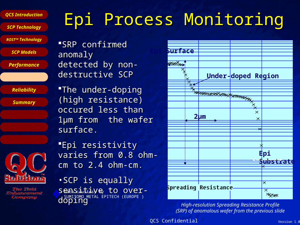
Epi Process MonitoringEpi Process Monitoring
2µm
Epi Surface
EpiSubstrate
Under-doped Region
SRP confirmed anomaly SRP confirmed anomaly detected by non-detected by non-destructive SCPdestructive SCP
The under-doping (high The under-doping (high resistance) occured less resistance) occured less than 1µm from the wafer than 1µm from the wafer surface.surface.
Epi resistivity varies from Epi resistivity varies from 0.8 ohm-cm to 2.4 ohm-0.8 ohm-cm to 2.4 ohm-cm.cm.
•SCP is equally sensitive to SCP is equally sensitive to over-dopingover-doping..
High-resolution Spreading Resistance Profile (SRP) of anomalous wafer from the previous
slide
Data courtesy bySUMITOMO METAL EPITECH (EUROPE )

Slide 41
QCS Confidential Version 1.0
SCP Models
QCS Introduction
SCP Technology
ROSTTM Technology
Performance
Examples
Reliability
Summary
Customer Monitor Wafer and Customer Monitor Wafer and Production Buried Layer ResultsProduction Buried Layer Results
Buried Layer Product Wafer
SCP eliminates the need for monitor wafers!
Monitor Wafer

Slide 42
QCS Confidential Version 1.0
SCP Models
QCS Introduction
SCP Technology
ROSTTM Technology
Performance
Examples
Reliability
Summary
SCP Detects Auto DopingSCP Detects Auto Doping
Map of Doping Level Device BV pass/fail map
SCP detects edge autodoping that affects Breakdown Voltage
low resistivity area => low BV devices
MC. NGUYEN - SUMITOMO METAL EPITECH MC. NGUYEN - SUMITOMO METAL EPITECH 196th ECS Meeting, Honolulu, October 1999 196th ECS Meeting, Honolulu, October 1999
Slide 43
QCS Confidential Version 1.0
SCP Models
QCS Introduction
SCP Technology
ROSTTM Technology
Performance
Examples
Reliability
Summary
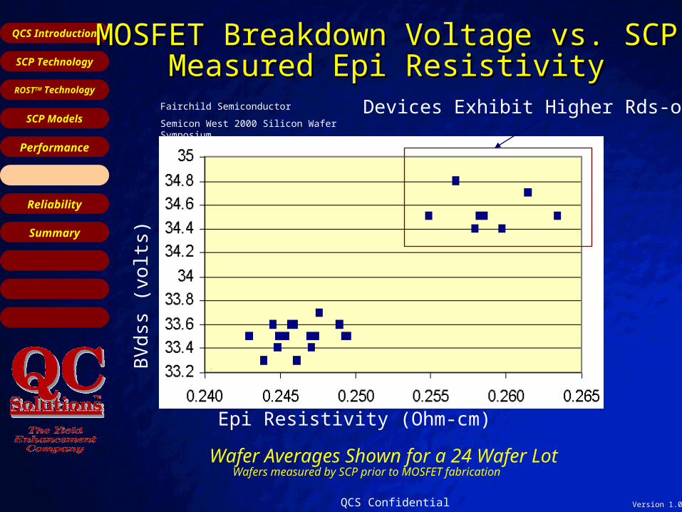
MOSFET Breakdown Voltage vs. SCP MOSFET Breakdown Voltage vs. SCP Measured Epi ResistivityMeasured Epi Resistivity
Epi Resistivity (Ohm-cm)
BV
dss
(vo
lts)
Devices Exhibit Higher Rds-on
Wafer Averages Shown for a 24 Wafer Lot
Fairchild Semiconductor
Semicon West 2000 Silicon Wafer Symposium
Wafers measured by SCP prior to MOSFET fabrication

Slide 44
QCS Confidential Version 1.0
SCP Models
QCS Introduction
SCP Technology
ROSTTM Technology
Performance
Examples
Reliability
Summary
Autodoping Effects in a Barrel ReactorAutodoping Effects in a Barrel Reactor
• Undoped epi growth on n-type 6-inch substrates
• No backseal used
20 Ohm-cm Substrates
Row 1
Row 2
5000 Ohm-cm
4000
3000
2000
0
1000
0.02 Ohm-cm Substrates600 Ohm-cm
480
360
240
0
120
Gas Flow
Autodoping source is mainly the high doping level of substrates

Slide 45
QCS Confidential Version 1.0
SCP Models
QCS Introduction
SCP Technology
ROSTTM Technology
Performance
Examples
Reliability
Summary
Susceptor Failure DetectionSusceptor Failure Detection
SusceptorRotation
Gas Flow
Location ofa Pinhole inthe susceptorcoating.
Resistivity Maps of 125mm N-type Epi(arranged as-grown in epi reactor)
95 Ohm-cm
90
85
80
75
70 Ohm-cm
Slide 46
QCS Confidential Version 1.0
SCP Models
QCS Introduction
SCP Technology
ROSTTM Technology
Performance
Examples
Reliability
Summary
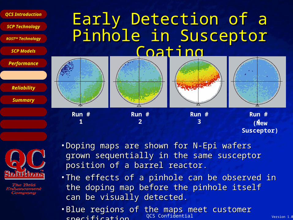
Early Detection of a Pinhole in Early Detection of a Pinhole in Susceptor CoatingSusceptor Coating
• Doping maps are shown for N-Epi wafers grown Doping maps are shown for N-Epi wafers grown sequentially in the same susceptor position of a barrel sequentially in the same susceptor position of a barrel reactor. reactor.
• The effects of a pinhole can be observed in the doping The effects of a pinhole can be observed in the doping map before the pinhole itself can be visually detected. map before the pinhole itself can be visually detected.
• Blue regions of the maps meet customer specification.Blue regions of the maps meet customer specification.
Run # 2 Run # 3 Run # 4
(New Susceptor)
Run # 1

Slide 47
QCS Confidential Version 1.0
SCP Models
QCS Introduction
SCP Technology
ROSTTM Technology
Performance
Examples
Reliability
Summary
Ion Implantation MonitoringIon Implantation Monitoring
Substrate
SCP Map After Ion Implantation before EpiSCP Map After Ion Implantation before Epi
SubstrateEpi
SCP Map After Ion Implantation & EpiSCP Map After Ion Implantation & Epi
Effect on yield of misclamping during Ion ImplantationEffect on yield of misclamping during Ion Implantation(Medium Current Implant)(Medium Current Implant)

Slide 48
QCS Confidential Version 1.0
SCP Models
QCS Introduction
SCP Technology
ROSTTM Technology
Performance
Examples
Reliability
Summary System ReliabilitySystem Reliability
Slide 49
QCS Confidential Version 1.0
SCP Models
QCS Introduction
SCP Technology
ROSTTM Technology
Performance
Examples
Reliability
Summary
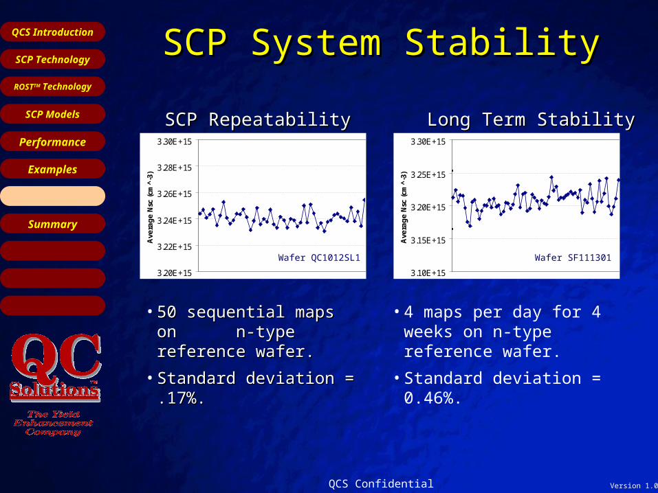
SCP System StabilitySCP System Stability
SCP RepeatabilitySCP Repeatability
3.20E+15
3.22E+15
3.24E+15
3.26E+15
3.28E+15
3.30E+15A
vera
ge
Nsc
(cm
^-3
)
Wafer QC1012SL1
• 50 50 sequential maps on sequential maps on n-type reference wafer.n-type reference wafer.
• Standard deviation = .17%.Standard deviation = .17%.
3.10E+15
3.15E+15
3.20E+15
3.25E+15
3.30E+15
Ave
rag
e N
sc (
cm^
-3)
Long Term StabilityLong Term Stability
Wafer SF111301
• 4 maps per day for 4 weeks on n-type reference wafer.
• Standard deviation = 0.46%.

Slide 50
QCS Confidential Version 1.0
SCP Models
QCS Introduction
SCP Technology
ROSTTM Technology
Performance
Examples
Reliability
Summary
Daily RepeatabilityDaily RepeatabilityDay 1 Day 2 Day 3 Day 4Day 1 Day 2 Day 3 Day 4

Slide 51
QCS Confidential Version 1.0
SCP Models
QCS Introduction
SCP Technology
ROSTTM Technology
Performance
Examples
Reliability
Summary
SCP Measurement: No Particle ContaminationSCP Measurement: No Particle Contamination
LETI France December 97 SCP 7200
151413121110
987654321
151413121110
987654321
109876
15 wafers out of the shipment box SCP measurements on wafers 6 to 101000 point map 5 times
cassettebottom
top
After measurement same history for the 15 wafers
Incoming inspection : optical test with TENCORsum of defects - particles @ 0.2µm
Wafer12 345
Defects2 5 222
Wafer67 8910
Defects6 1 625
Wafer1112 131415
Defects0 2 447
Wafer12 345
Defects2 4 233
Wafer67 8910
Defects7 1 626
Wafer1112 131415
Defects0 5 16716
Inspection after measurement : optical test with TENCORsum of defects - particles @ 0.2µm

Slide 52
QCS Confidential Version 1.0
SCP Models
QCS Introduction
SCP Technology
ROSTTM Technology
Performance
Examples
Reliability
Summary
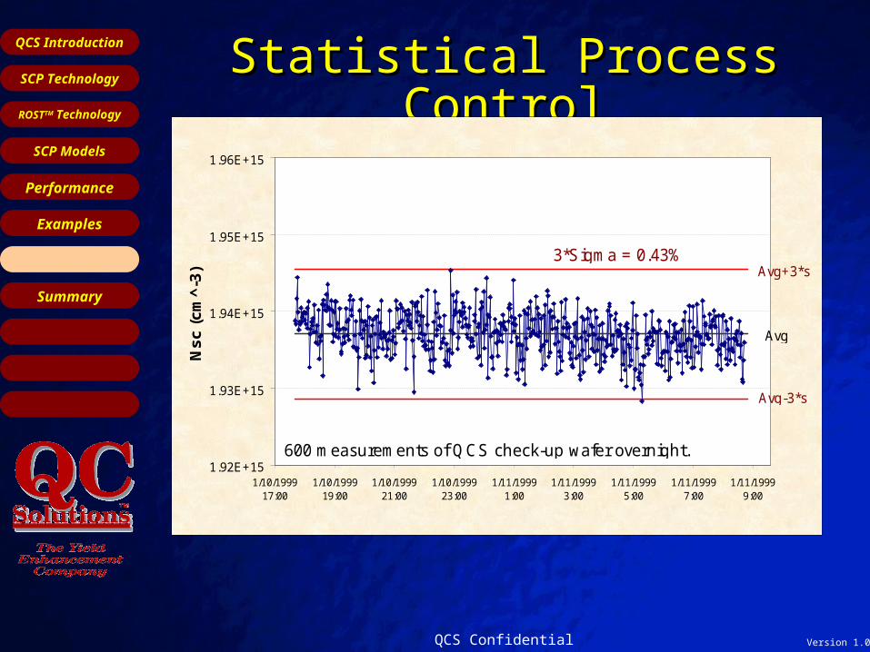
Statistical Process ControlStatistical Process Control
DopantGas Flow
Production wafers straight out of the epi reactor, specification: 54 Ohm.cm 10% 500 point maps.
3E14
2E14
SCP 500 point doping maps (at/cm3)
Multi-Position BarrelFace # 7
45
47
49
51
53
55
57
59
61
63
65
0 5 10 15 20 25 30 35 40 45 50
Wafer Number R
esis
tivity
(O
hm.c
m)
LCL : 54 - 10%
UCL : 54 + 10%
run 1 run 2 run 3
2.1
2.2
2.3
Top
Bottom
2.48E14
2.36E14
2.38E14
Spec.54
Slide 53
QCS Confidential Version 1.0
SCP Models
QCS Introduction
SCP Technology
ROSTTM Technology
Performance
Examples
Reliability
Summary
Statistical Process ControlStatistical Process Control
1.92E+15
1.93E+15
1.94E+15
1.95E+15
1.96E+15
1/10/199917:00
1/10/199919:00
1/10/199921:00
1/10/199923:00
1/11/19991:00
1/11/19993:00
1/11/19995:00
1/11/19997:00
1/11/19999:00
Ns
c (
cm
^-3
)
3*Sigma = 0.43%
Avg
Avg+3*s
Avg-3*s
600 measurements of QCS check-up wafer overnight.

Slide 54
QCS Confidential Version 1.0
SCP Models
QCS Introduction
SCP Technology
ROSTTM Technology
Performance
Examples
Reliability
Summary
Summary: QCS-7000 Surface Summary: QCS-7000 Surface Charge ProfilerCharge Profiler
• Non-destructive resistivity measurement of product wafersNon-destructive resistivity measurement of product wafers Elimination of monitor wafers and associated costsElimination of monitor wafers and associated costs
Conventional (CMOS) EpiConventional (CMOS) Epi Specialty Epi (devices: power, wireless, linear)Specialty Epi (devices: power, wireless, linear)
• FeaturesFeatures Rapid, full wafer mappingRapid, full wafer mapping
Aids process development, better visualize process resultsAids process development, better visualize process results
Shows subtle problems earlierShows subtle problems earlier Correlates extremely well with traditional measurement Correlates extremely well with traditional measurement
techniques.techniques. Even more important: SCP Maps correlate with FINAL device Even more important: SCP Maps correlate with FINAL device
parameters!parameters! Surface sensitivity detects deposition problems that may escape Surface sensitivity detects deposition problems that may escape
conventional techniquesconventional techniques No preprocessing required for fresh wafersNo preprocessing required for fresh wafers