Silicon photonics: Waveguide modulators and...
99
2572-12 Winter College on Optics: Fundamentals of Photonics - Theory, Devices and Applications Laurent Vivien 10 - 21 February 2014 Institut dElectronique Fondamentale CNRS UMR 8622, Université Paris Sud 91405 Orsay Cedex FRANCE Silicon photonics: Integrated modulators and detectors
Transcript of Silicon photonics: Waveguide modulators and...

2572-12
Winter College on Optics: Fundamentals of Photonics - Theory, Devices and Applications
Laurent Vivien
10 - 21 February 2014
Institut d�Electronique Fondamentale CNRS UMR 8622, Université Paris Sud
91405 Orsay Cedex FRANCE France
Silicon photonics: Integrated modulators and detectors
Silicon PhotonicsSilicon-based micro and nanophotonic devices
http://silicon-photonics.ief.u-psud.fr/ 1
Silicon photonics:Integrated modulators and detectors
Laurent VivienInstitut d’Electronique Fondamentale, CNRS UMR 8622,
Université Paris Sud, 91405 Orsay Cedex, France
http://silicon-photonics.ief.u-psud.fr/
Silicon PhotonicsSilicon-based micro and nanophotonic devices
http://silicon-photonics.ief.u-psud.fr/ 2
Silicon photonics:Waveguide modulators and detectors
L. Vivien,
D. Marris-Morini, G. Rasigade, L. Virot, M. Ziebell, D. Perez-Galacho, P. Chaisakul, M-S. Rouifed, P. Crozat, P. Damas, E. Cassan
D. Bouville, S. Edmond, X. Le RouxInstitut d’Electronique Fondamentale, CNRS UMR 8622,
Université Paris Sud, 91405 Orsay Cedex, Francehttp://silicon-photonics.ief.u-psud.fr/
J-M. Fédéli, S, Olivier, Jean Michel Hartmann
CEA-LETI, Minatec 17 rue des Martyrs, 38054 Grenoble cedex 9, France
G. Isella, D. Chrastina, J. FrigerioL-NESS, Politecnico di Milano, Polo di Como, Via Anzani 42, I-22100 Como, Italy
C. Baudot, F. BoeufSTMicroelectronics, Silicon Technology Development, Crolles, France
http://silicon-photonics.ief.u-psud.fr/ Laurent Vivien3
Outline
Motivation Silicon photonics in two words!
Photodetectors on silicon Main characteristics Main results
Optical modulators Figures of Merit Modulation in silicon Main results
Electronic-Photonic convergence
Conclusion
http://silicon-photonics.ief.u-psud.fr/ Laurent Vivien4
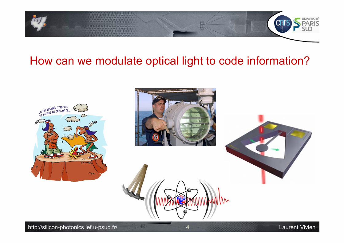
How can we modulate optical light to code information?
http://silicon-photonics.ief.u-psud.fr/ Laurent Vivien
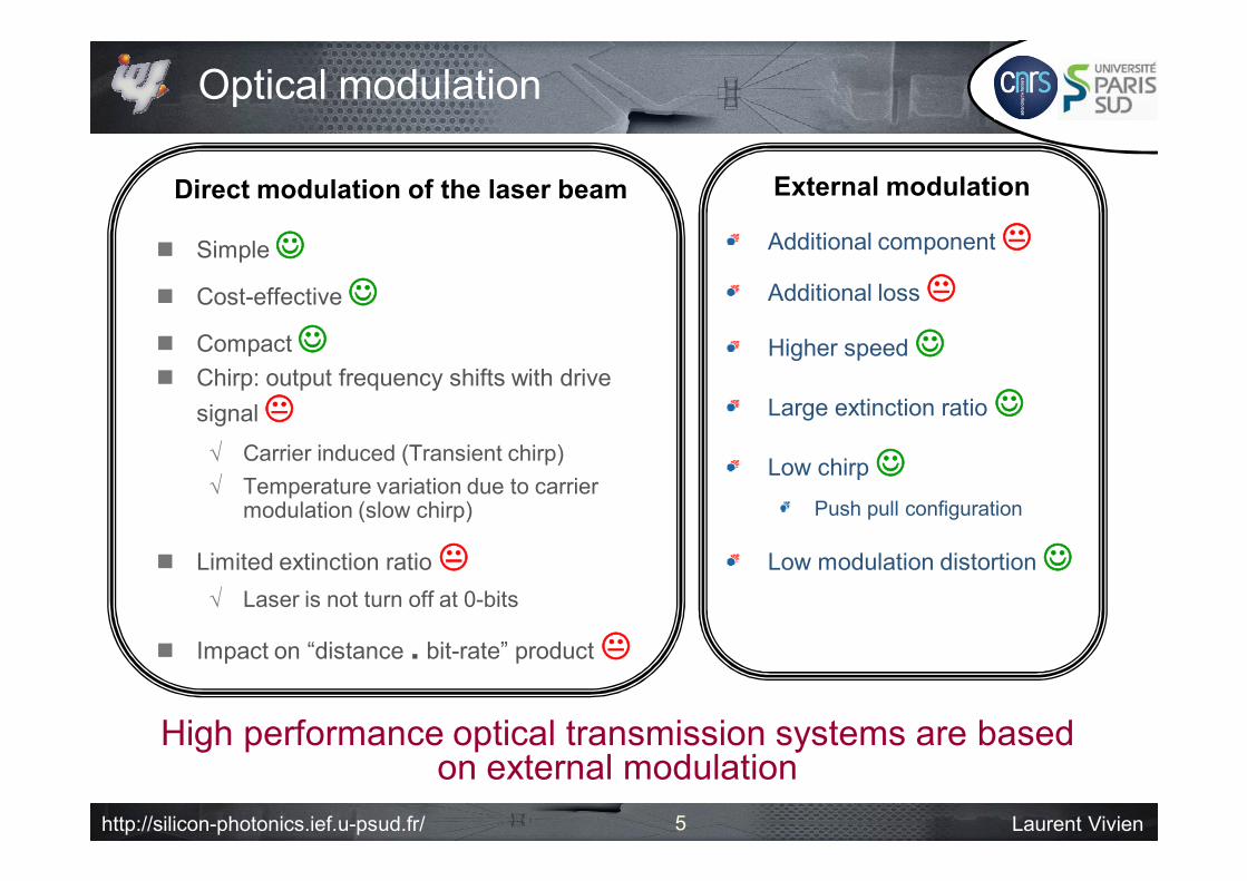
Optical modulation
Simple Cost-effective Compact Chirp: output frequency shifts with drive
signal Carrier induced (Transient chirp) Temperature variation due to carrier
modulation (slow chirp)
Limited extinction ratio Laser is not turn off at 0-bits
Impact on “distance . bit-rate” product
Additional component
Additional loss
Higher speed
Large extinction ratio
Low chirp Push pull configuration
Low modulation distortion
Direct modulation of the laser beam External modulation
High performance optical transmission systems are based on external modulation
5
http://silicon-photonics.ief.u-psud.fr/ Laurent Vivien
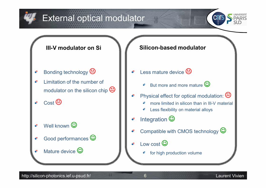
External optical modulator
Bonding technology Limitation of the number of
modulator on the silicon chip
Cost
Well known
Good performances
Mature device
III-V modulator on Si
Less mature device
But more and more mature
Physical effect for optical modulation: more limited in silicon than in III-V materialLess flexibility on material alloys
Integration
Compatible with CMOS technology
Low cost for high production volume
Silicon-based modulator
6
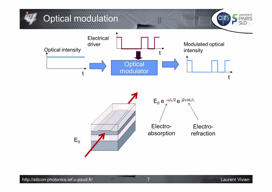
http://silicon-photonics.ief.u-psud.fr/ Laurent Vivien7
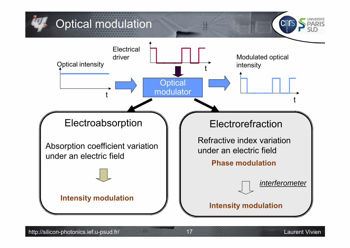
Optical modulation
Opticalmodulatort
Optical intensity
Electrical driver
t
Modulated optical intensityt
E0
Electro-absorption
Electro-refraction
E0 e –L/2 e j2nL/
http://silicon-photonics.ief.u-psud.fr/ Laurent Vivien8
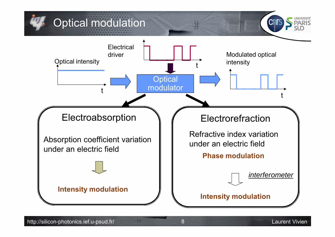
Optical modulation
Opticalmodulatort
Optical intensity
Electrical driver
t
Modulated optical intensityt
Electroabsorption
Phase modulation
Intensity modulation
interferometer
Intensity modulation
Electrorefraction
Absorption coefficient variation under an electric field
Refractive index variation under an electric field
http://silicon-photonics.ief.u-psud.fr/ Laurent Vivien9
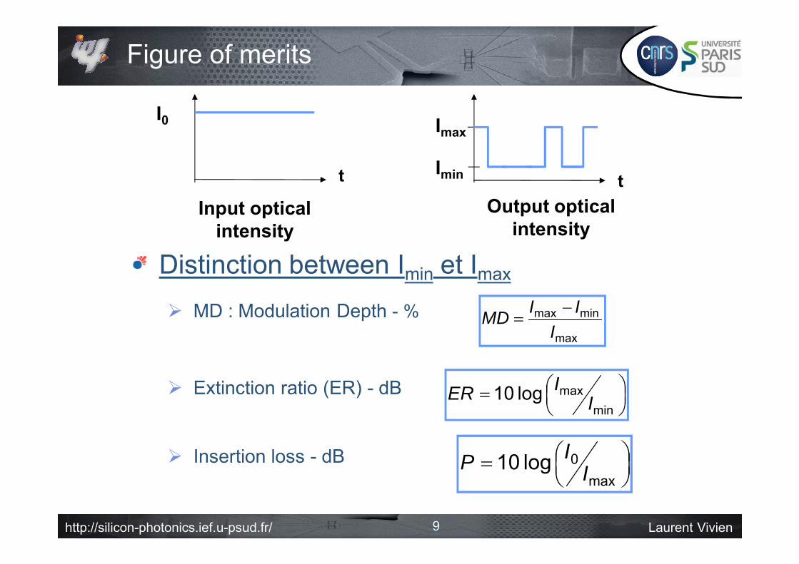
Figure of merits
Distinction between Imin et Imax
MD : Modulation Depth - %
Extinction ratio (ER) - dB
Insertion loss - dB
max
minmax
IIIMD
minmaxlog10 IIER
Output optical intensity
tImin
Imax
Input optical intensity
t
I0
max0log10 I
IP
9
http://silicon-photonics.ief.u-psud.fr/ Laurent Vivien10
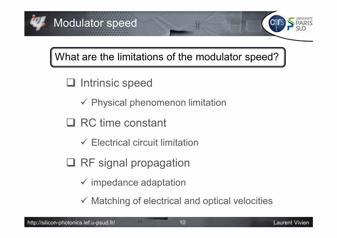
Modulator speed
Intrinsic speed
Physical phenomenon limitation
RC time constant
Electrical circuit limitation
RF signal propagation
impedance adaptation
Matching of electrical and optical velocities
What are the limitations of the modulator speed?
http://silicon-photonics.ief.u-psud.fr/ Laurent Vivien11
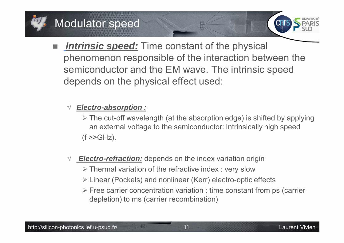
Modulator speed
Intrinsic speed: Time constant of the physical phenomenon responsible of the interaction between the semiconductor and the EM wave. The intrinsic speed depends on the physical effect used:
Electro-absorption : The cut-off wavelength (at the absorption edge) is shifted by applying
an external voltage to the semiconductor: Intrinsically high speed (f >>GHz).
Electro-refraction: depends on the index variation origin Thermal variation of the refractive index : very slow Linear (Pockels) and nonlinear (Kerr) electro-optic effects Free carrier concentration variation : time constant from ps (carrier
depletion) to ms (carrier recombination)
http://silicon-photonics.ief.u-psud.fr/ Laurent Vivien12
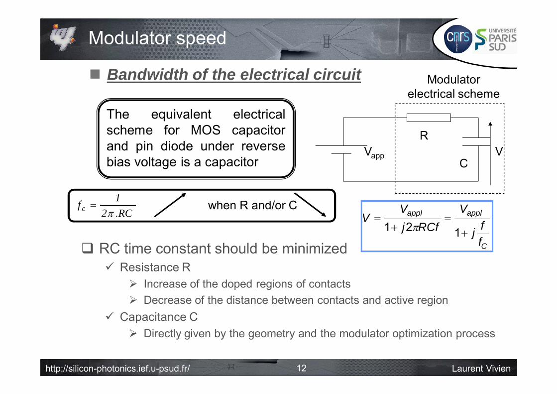
Modulator speed
Bandwidth of the electrical circuit
C
applappl
ffj
VRCfj
VV
121
R
CVVapp
RC time constant should be minimized Resistance R
Increase of the doped regions of contacts Decrease of the distance between contacts and active region
Capacitance C Directly given by the geometry and the modulator optimization process
The equivalent electricalscheme for MOS capacitorand pin diode under reversebias voltage is a capacitor
RC21fc .
when R and/or C
Modulator electrical scheme
http://silicon-photonics.ief.u-psud.fr/ Laurent Vivien13
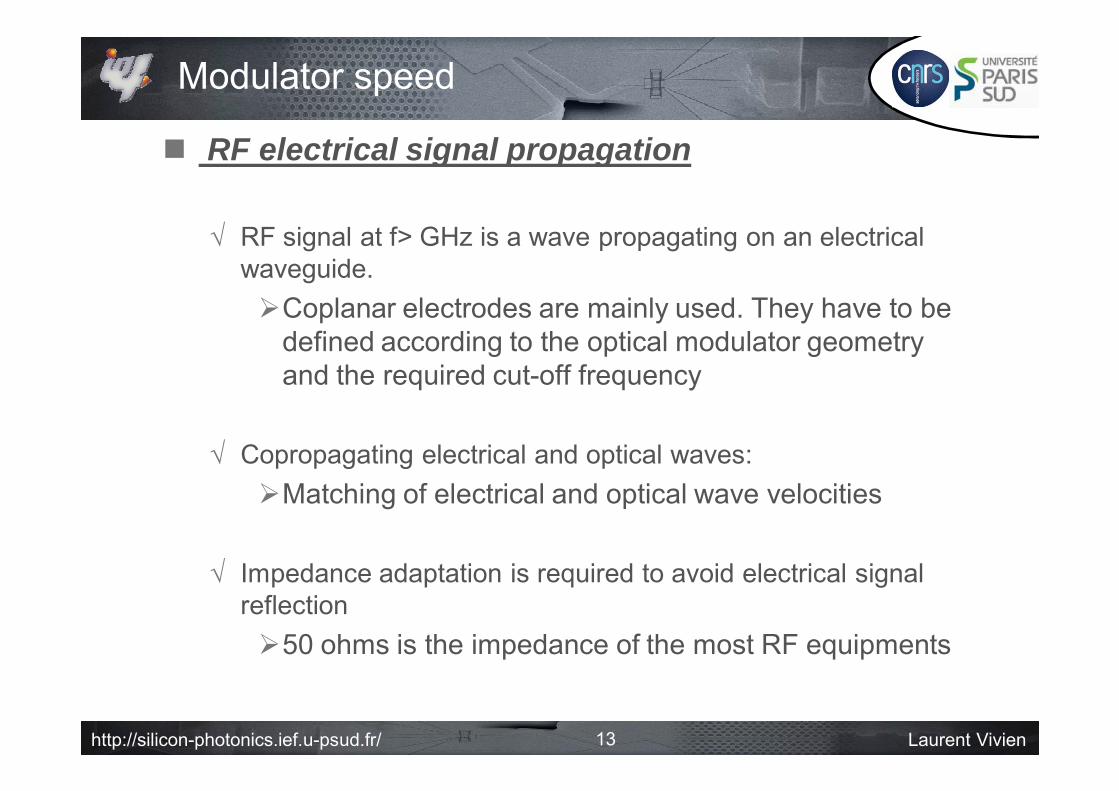
Modulator speed
RF electrical signal propagation
RF signal at f> GHz is a wave propagating on an electrical waveguide.Coplanar electrodes are mainly used. They have to be
defined according to the optical modulator geometry and the required cut-off frequency
Copropagating electrical and optical waves:Matching of electrical and optical wave velocities
Impedance adaptation is required to avoid electrical signal reflection50 ohms is the impedance of the most RF equipments

http://silicon-photonics.ief.u-psud.fr/ Laurent Vivien
Energy consumption
14
Energy to charge the deviceEnergy/bit = 1/4 (CVpp)2
Energy dissipation of photocurrentEnergy/bit = 1/B (IphVbias)
R
CVVapp
Modulator electrical scheme
How can we reduce the energy consumption?
http://silicon-photonics.ief.u-psud.fr/ Laurent Vivien
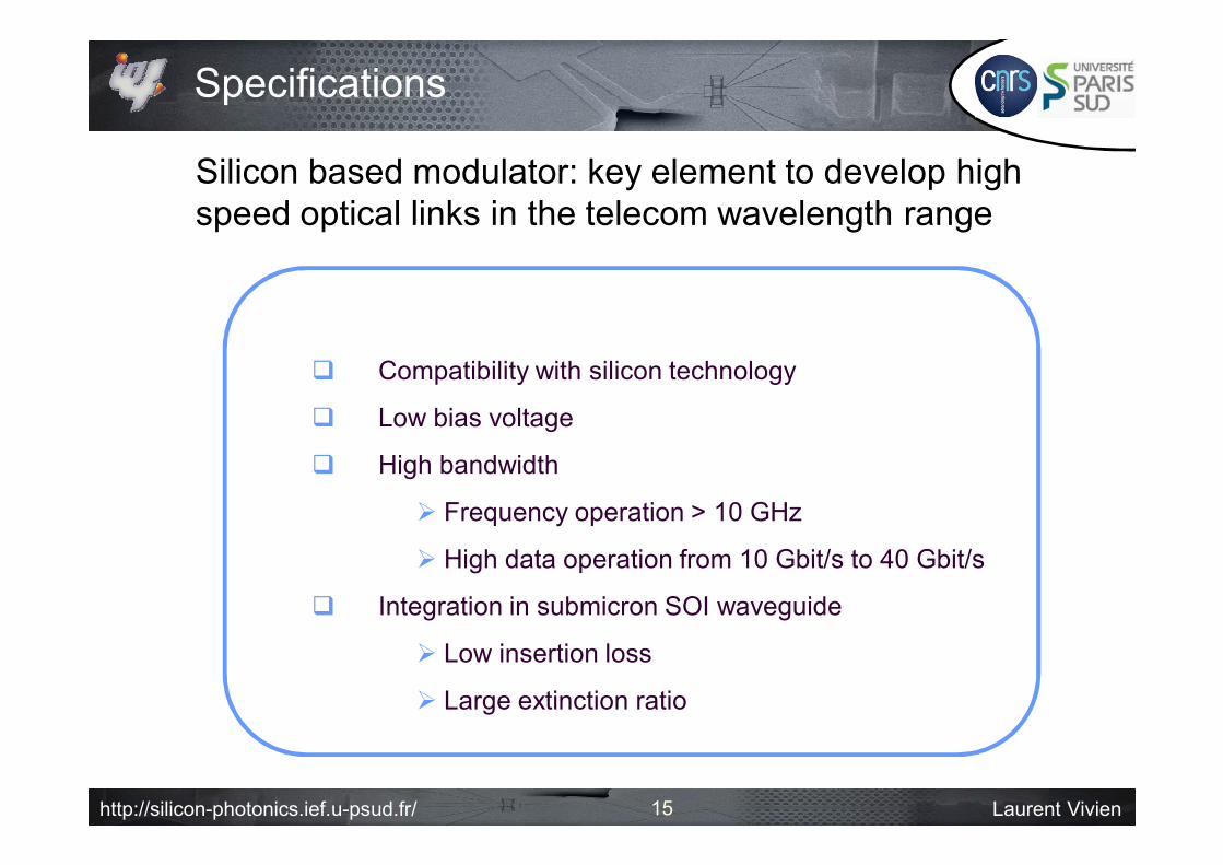
Specifications
Silicon based modulator: key element to develop high speed optical links in the telecom wavelength range
Compatibility with silicon technology
Low bias voltage
High bandwidth
Frequency operation > 10 GHz
High data operation from 10 Gbit/s to 40 Gbit/s
Integration in submicron SOI waveguide
Low insertion loss
Large extinction ratio
15
http://silicon-photonics.ief.u-psud.fr/ Laurent Vivien16
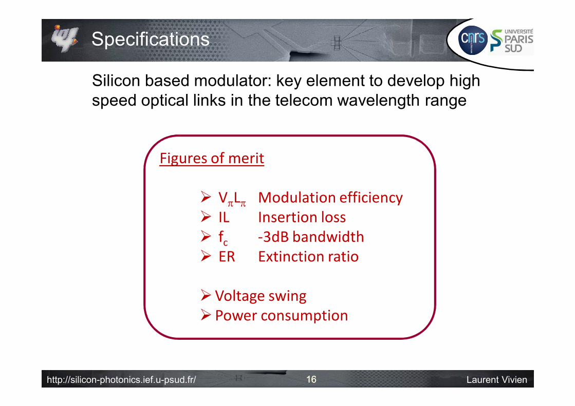
Specifications
Silicon based modulator: key element to develop high speed optical links in the telecom wavelength range
16
Figures of merit
VL Modulation efficiency IL Insertion loss fc ‐3dB bandwidth ER Extinction ratio
Voltage swingPower consumption
http://silicon-photonics.ief.u-psud.fr/ Laurent Vivien17
Optical modulation
Opticalmodulatort
Optical intensity
Electrical driver
t
Modulated optical intensityt
Electroabsorption
Phase modulation
Intensity modulation
interferometer
Intensity modulation
Electrorefraction
Absorption coefficient variation under an electric field
Refractive index variation under an electric field
http://silicon-photonics.ief.u-psud.fr/ Laurent Vivien
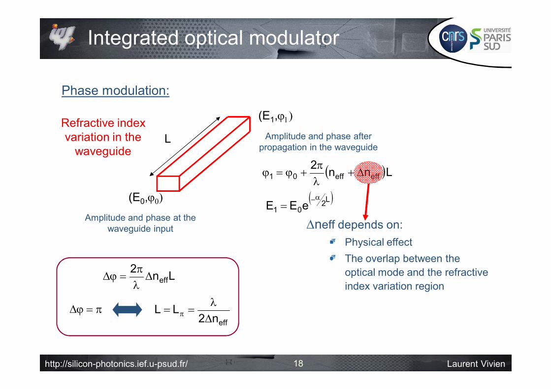
Integrated optical modulator
Phase modulation:
Lnn2effeff01
(E0,
(E1,
Amplitude and phase at the waveguide input
Amplitude and phase after propagation in the waveguide
LRefractive index variation in the
waveguide
neff depends on:Physical effectThe overlap between the optical mode and the refractive index variation region
Ln2eff
effn2LL
L201 eEE
18
http://silicon-photonics.ief.u-psud.fr/ Laurent Vivien
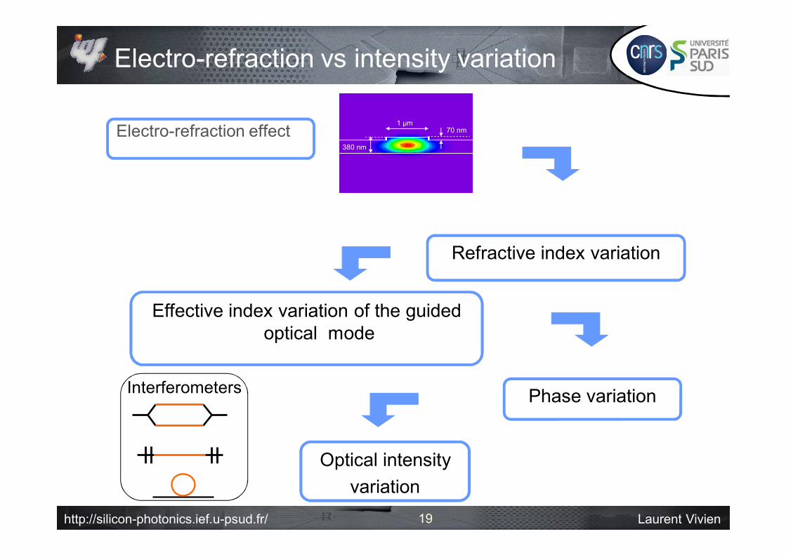
Electro-refraction vs intensity variation
Electro-refraction effect
Refractive index variation
Effective index variation of the guided optical mode
Phase variation
Optical intensityvariation
Interferometers
1 µm
380 nm
70 nm1 µm
380 nm
70 nm
19
http://silicon-photonics.ief.u-psud.fr/ Laurent Vivien
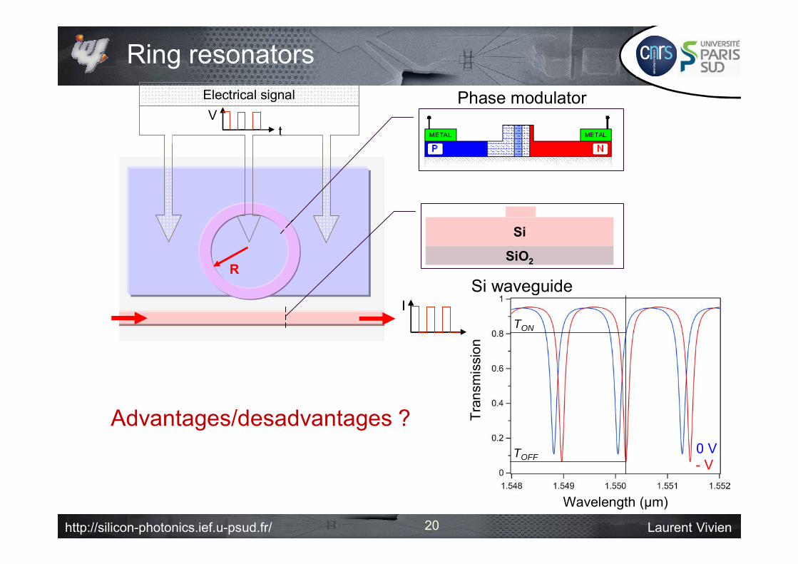
Ring resonators
t
I
t
I
tV
Electrical signal
R
Si
SiO2
Phase modulator
Si waveguide
TOFF
TON
0 V- V
TOFF
TON
0 V- V
Wavelength (µm)
Tran
smis
sion
Advantages/desadvantages ?
20
http://silicon-photonics.ief.u-psud.fr/ Laurent Vivien
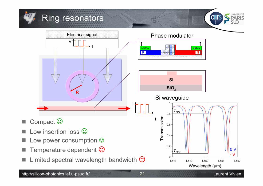
Ring resonators
Compact Low insertion loss Low power consumption Temperature dependent Limited spectral wavelength bandwidth
t
I
t
I
tV
Electrical signal
R
Si
SiO2
Phase modulator
Si waveguide
TOFF
TON
0 V- V
TOFF
TON
0 V- V
Wavelength (µm)Tr
ansm
issi
on
21
http://silicon-photonics.ief.u-psud.fr/ Laurent Vivien
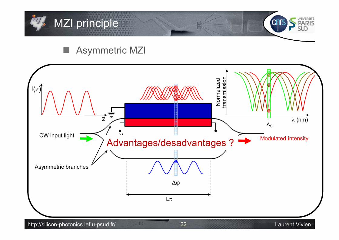
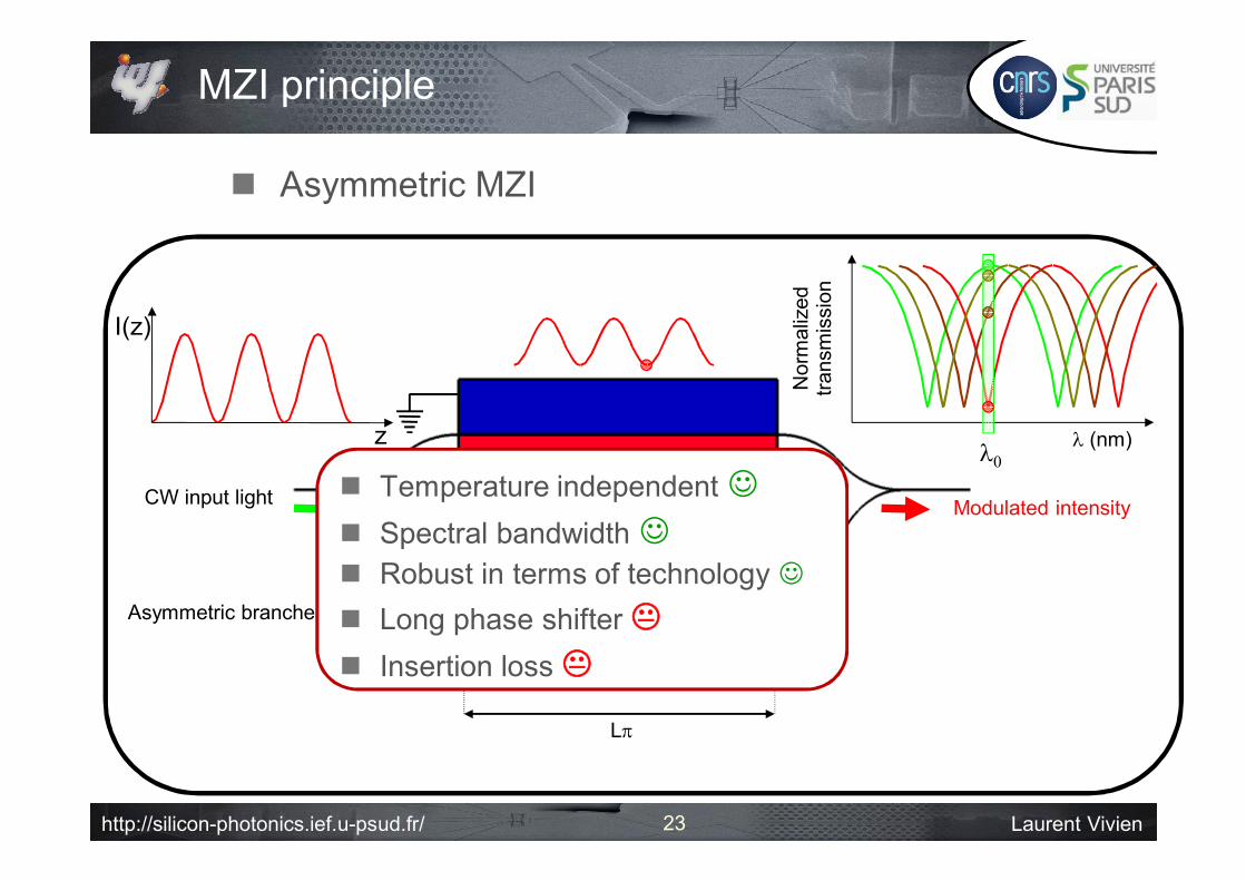
MZI principle
Asymmetric MZI
V
Asymmetric branches
CW input light Modulated intensity
L
I(z)
z
Nor
mal
ized
tra
nsm
issi
on
(nm)
Advantages/desadvantages ?
22
http://silicon-photonics.ief.u-psud.fr/ Laurent Vivien
MZI principle
Asymmetric MZI
V
Asymmetric branches
CW input light Modulated intensity
L
I(z)
z
Nor
mal
ized
tra
nsm
issi
on
(nm) Temperature independent Spectral bandwidth Robust in terms of technology Long phase shifter Insertion loss
23
http://silicon-photonics.ief.u-psud.fr/ Laurent Vivien24
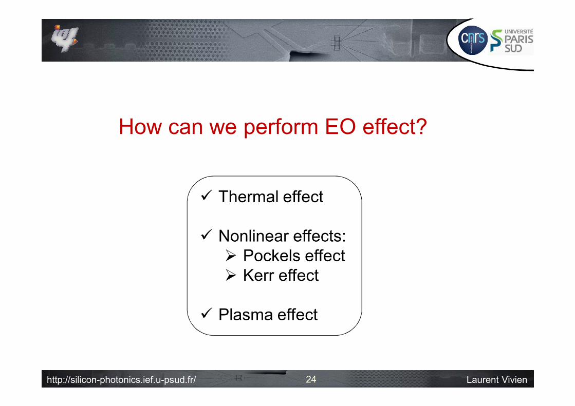
How can we perform EO effect?
Thermal effect
Nonlinear effects: Pockels effect Kerr effect
Plasma effect
http://silicon-photonics.ief.u-psud.fr/ Laurent Vivien
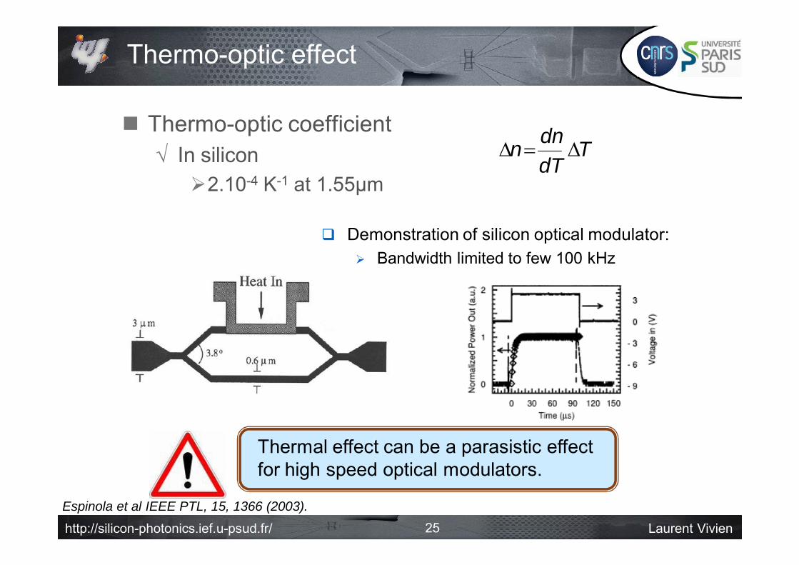
Thermo-optic effect
TdTdnn
Demonstration of silicon optical modulator: Bandwidth limited to few 100 kHz
Espinola et al IEEE PTL, 15, 1366 (2003).
Thermal effect can be a parasistic effect for high speed optical modulators.
Thermo-optic coefficient In silicon2.10-4 K-1 at 1.55µm
25
http://silicon-photonics.ief.u-psud.fr/ Laurent Vivien
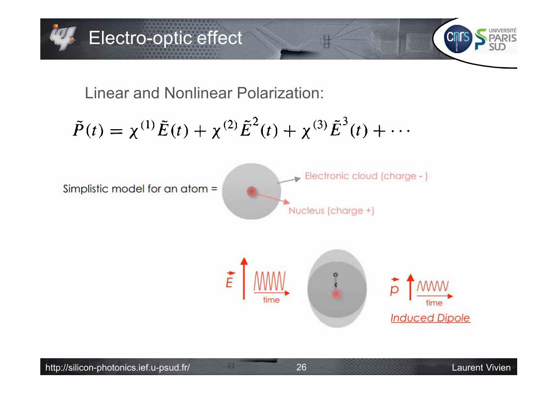
Electro-optic effect
26
Linear and Nonlinear Polarization:

http://silicon-photonics.ief.u-psud.fr/ Laurent Vivien
Electro-optic effect
27
Pockels effect:Linear electro-optic effect
Wavelength conversion Second Harmonic Generation (SHG)
Kerr effect:Nonlinear electro-optic effect
Wavelength conversionFour wave mixing (FWM)
>>
In siliconLinear and Nonlinear Polarization:
http://silicon-photonics.ief.u-psud.fr/ Laurent Vivien
Electro-optic effect
is it possible to obtain a linear electro-optic effect in silicon ?
28

http://silicon-photonics.ief.u-psud.fr/ Laurent Vivien
Electro-optic effect
29
Nonlinear Polarization:
Pockels effect:Linear electro-optic effect
Wavelength conversion Second Harmonic Generation (SHG)
Break the symmetry of silicon crystal
Strained silicon photonics
Without straining layer With straining
layer
http://silicon-photonics.ief.u-psud.fr/ Laurent Vivien
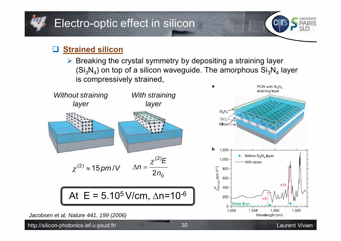
Electro-optic effect in silicon
Strained silicon Breaking the crystal symmetry by depositing a straining layer
(Si3N4) on top of a silicon waveguide. The amorphous Si3N4 layer is compressively strained,
Vpm /15)2( 0
)2(
2n
En
At E = 5.105 V/cm, n=10-6
Jacobsen et al, Nature 441, 199 (2006)
Without straining layer
With straining layer
30
http://silicon-photonics.ief.u-psud.fr/ Laurent Vivien
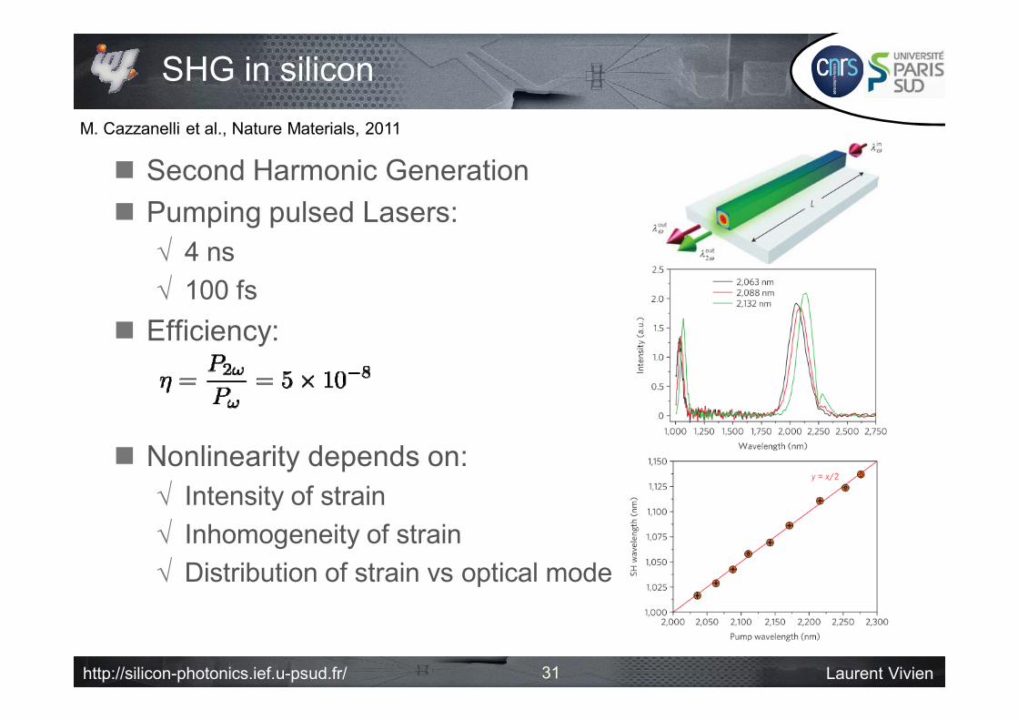
SHG in silicon
Second Harmonic Generation Pumping pulsed Lasers:
4 ns 100 fs
Efficiency:
Nonlinearity depends on: Intensity of strain Inhomogeneity of strain Distribution of strain vs optical mode
31
M. Cazzanelli et al., Nature Materials, 2011
http://silicon-photonics.ief.u-psud.fr/ Laurent Vivien
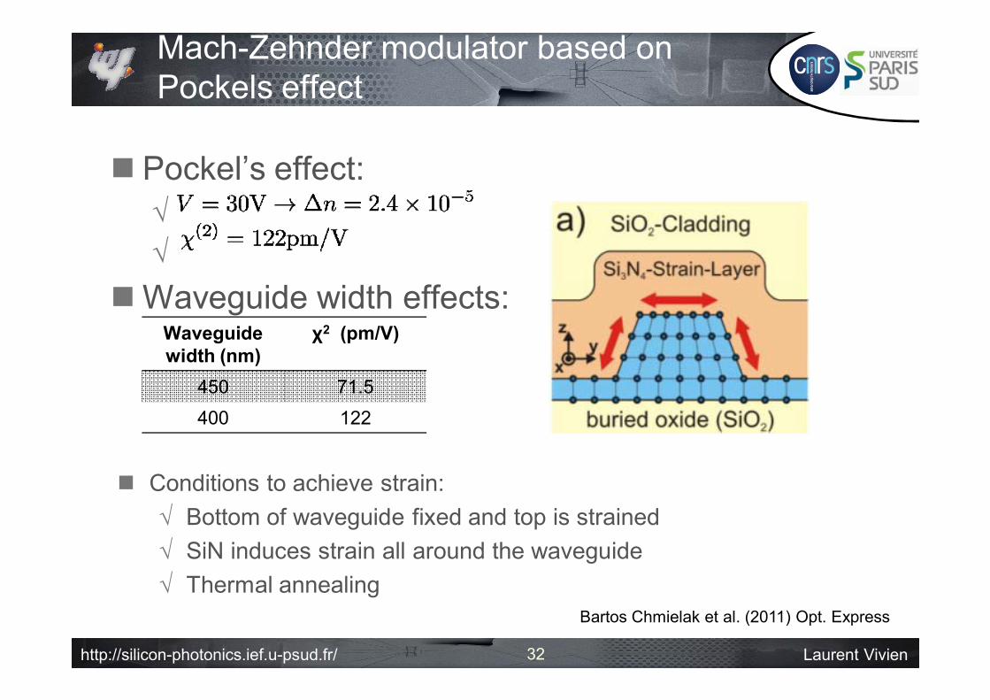
Mach-Zehnder modulator based on Pockels effect
Pockel’s effect:
Waveguide width effects:
Conditions to achieve strain: Bottom of waveguide fixed and top is strained SiN induces strain all around the waveguide Thermal annealing
32
Waveguide width (nm)
χ2 (pm/V)
450 71.5400 122
Bartos Chmielak et al. (2011) Opt. Express

http://silicon-photonics.ief.u-psud.fr/ Laurent Vivien
Electro-optic effect in silicon
Soref et al IEEE JQE QE-23 (1), (1987).
Free carrier density variation in silicon Refractive index are modified by free-carrier concentration
variations: Plasma dispersion effect
Free electrons Free holesC
arrie
r con
cent
ratio
n
33
http://silicon-photonics.ief.u-psud.fr/ Laurent Vivien
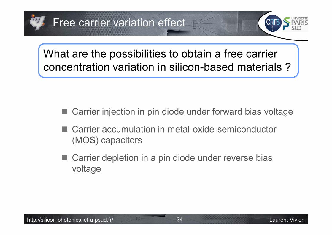
Free carrier variation effect
Carrier injection in pin diode under forward bias voltage
Carrier accumulation in metal-oxide-semiconductor(MOS) capacitors
Carrier depletion in a pin diode under reverse biasvoltage
What are the possibilities to obtain a free carrier concentration variation in silicon-based materials ?
34
http://silicon-photonics.ief.u-psud.fr/ Laurent Vivien
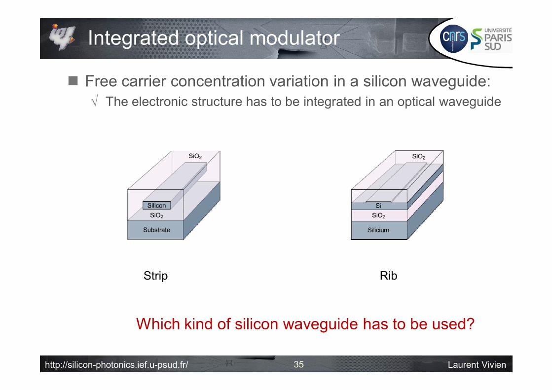
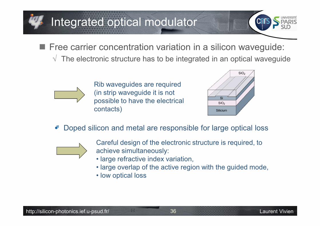
Integrated optical modulator
Free carrier concentration variation in a silicon waveguide: The electronic structure has to be integrated in an optical waveguide
Strip Rib
Which kind of silicon waveguide has to be used?
35
http://silicon-photonics.ief.u-psud.fr/ Laurent Vivien
Integrated optical modulator
Free carrier concentration variation in a silicon waveguide: The electronic structure has to be integrated in an optical waveguide
Rib waveguides are required(in strip waveguide it is not possible to have the electrical contacts)
Doped silicon and metal are responsible for large optical loss
Careful design of the electronic structure is required, to achieve simultaneously:• large refractive index variation,• large overlap of the active region with the guided mode, • low optical loss
36
http://silicon-photonics.ief.u-psud.fr/ Laurent Vivien
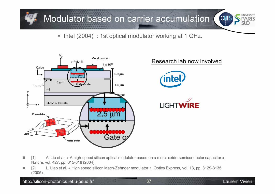
Modulator based on carrier accumulation
37
[1] A. Liu et al, « A high-speed silicon optical modulator based on a metal-oxide-semiconductor capacitor », Nature, vol. 427, pp. 615-618 (2004).
[2] L. Liao et al, « High speed silicon Mach-Zehnder modulator », Optics Express, vol. 13, pp. 3129-3135 (2005).
Intel (2004) : 1st optical modulator working at 1 GHz.
Research lab now involved
http://silicon-photonics.ief.u-psud.fr/ Laurent Vivien
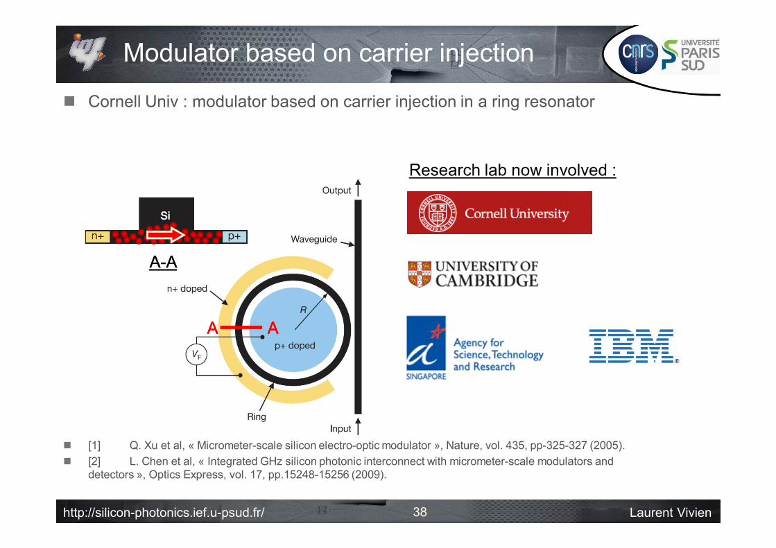
Modulator based on carrier injection
38
[1] Q. Xu et al, « Micrometer-scale silicon electro-optic modulator », Nature, vol. 435, pp-325-327 (2005). [2] L. Chen et al, « Integrated GHz silicon photonic interconnect with micrometer-scale modulators and
detectors », Optics Express, vol. 17, pp.15248-15256 (2009).
Cornell Univ : modulator based on carrier injection in a ring resonator
AA AAA A
A-AA-A
Research lab now involved :
http://silicon-photonics.ief.u-psud.fr/ Laurent Vivien
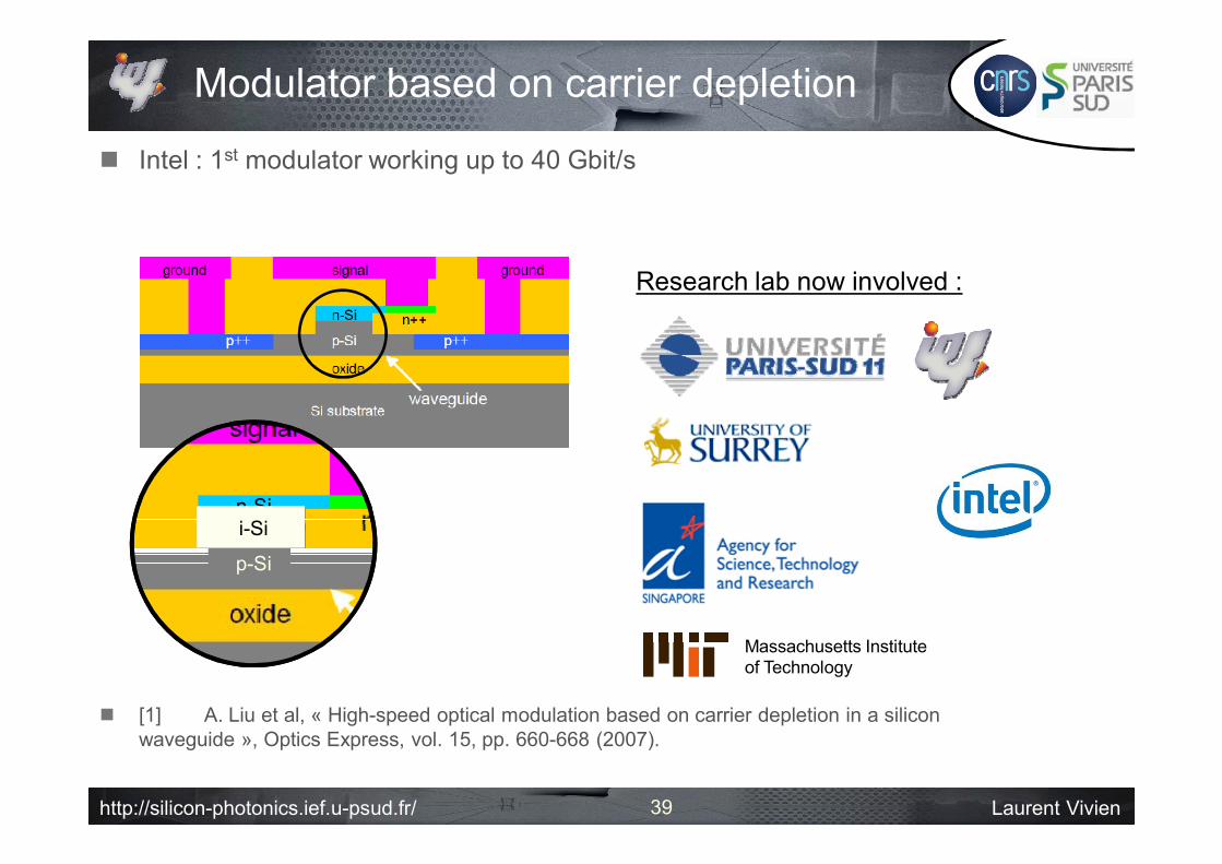
Modulator based on carrier depletion
39
[1] A. Liu et al, « High-speed optical modulation based on carrier depletion in a silicon waveguide », Optics Express, vol. 15, pp. 660-668 (2007).
Intel : 1st modulator working up to 40 Gbit/s
n-Si
p-Si
i-Si
Massachusetts Institute of Technology
Research lab now involved :
http://silicon-photonics.ief.u-psud.fr/ Laurent Vivien
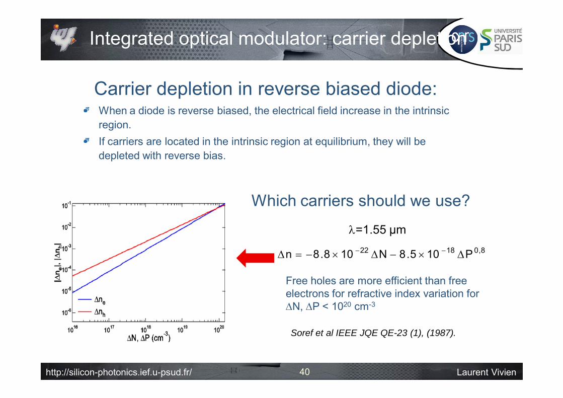
Integrated optical modulator: carrier depletion
Carrier depletion in reverse biased diode:When a diode is reverse biased, the electrical field increase in the intrinsic region.If carriers are located in the intrinsic region at equilibrium, they will be depleted with reverse bias.
Which carriers should we use?
Soref et al IEEE JQE QE-23 (1), (1987).
Free holes are more efficient than free electrons for refractive index variation for N, P < 1020 cm-3
8,01822 P105.8N108.8n
=1.55 µm
40
http://silicon-photonics.ief.u-psud.fr/ Laurent Vivien
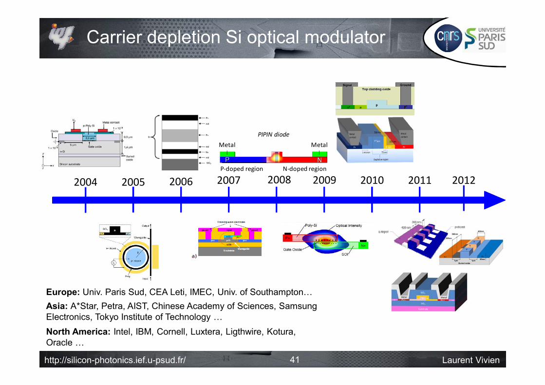
Carrier depletion Si optical modulator
2004 2005P‐doped region N‐doped region
PIPIN diodeMetal Metal
20082007 201120092006 2010
Europe: Univ. Paris Sud, CEA Leti, IMEC, Univ. of Southampton…Asia: A*Star, Petra, AIST, Chinese Academy of Sciences, Samsung Electronics, Tokyo Institute of Technology …North America: Intel, IBM, Cornell, Luxtera, Ligthwire, Kotura, Oracle …
2012
41
http://silicon-photonics.ief.u-psud.fr/ Laurent Vivien
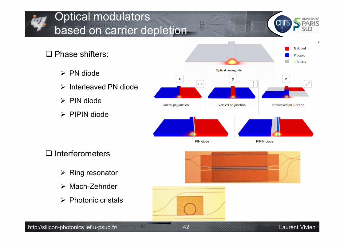
PIN diode PIPIN diode
Optical modulators based on carrier depletion
42
Phase shifters:
PN diode
Interleaved PN diode
PIN diode
PIPIN diode
Interferometers
Ring resonator
Mach-Zehnder
Photonic cristals
http://silicon-photonics.ief.u-psud.fr/ Laurent Vivien43
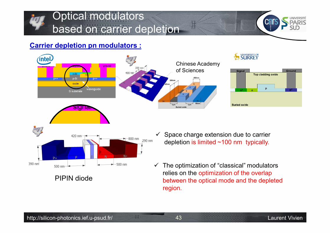
Carrier depletion pn modulators :
Space charge extension due to carrier depletion is limited ~100 nm typically.
n-Si
p-Sii-Si
The optimization of “classical” modulators relies on the optimization of the overlap between the optical mode and the depleted region.
Chinese Academy of Sciences
PIPIN diode
Optical modulators based on carrier depletion
http://silicon-photonics.ief.u-psud.fr/ Laurent Vivien44
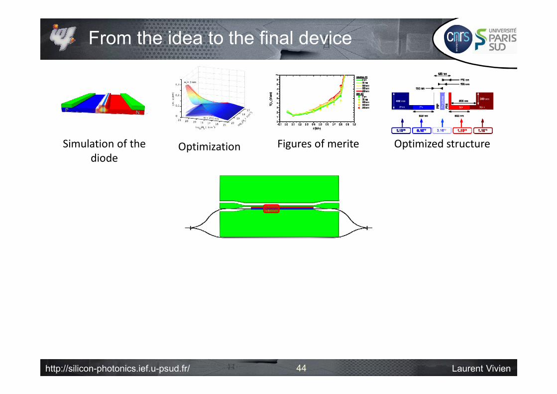
Simulation of the diode
Optimization Figures of merite Optimized structure
From the idea to the final device
http://silicon-photonics.ief.u-psud.fr/ Laurent Vivien
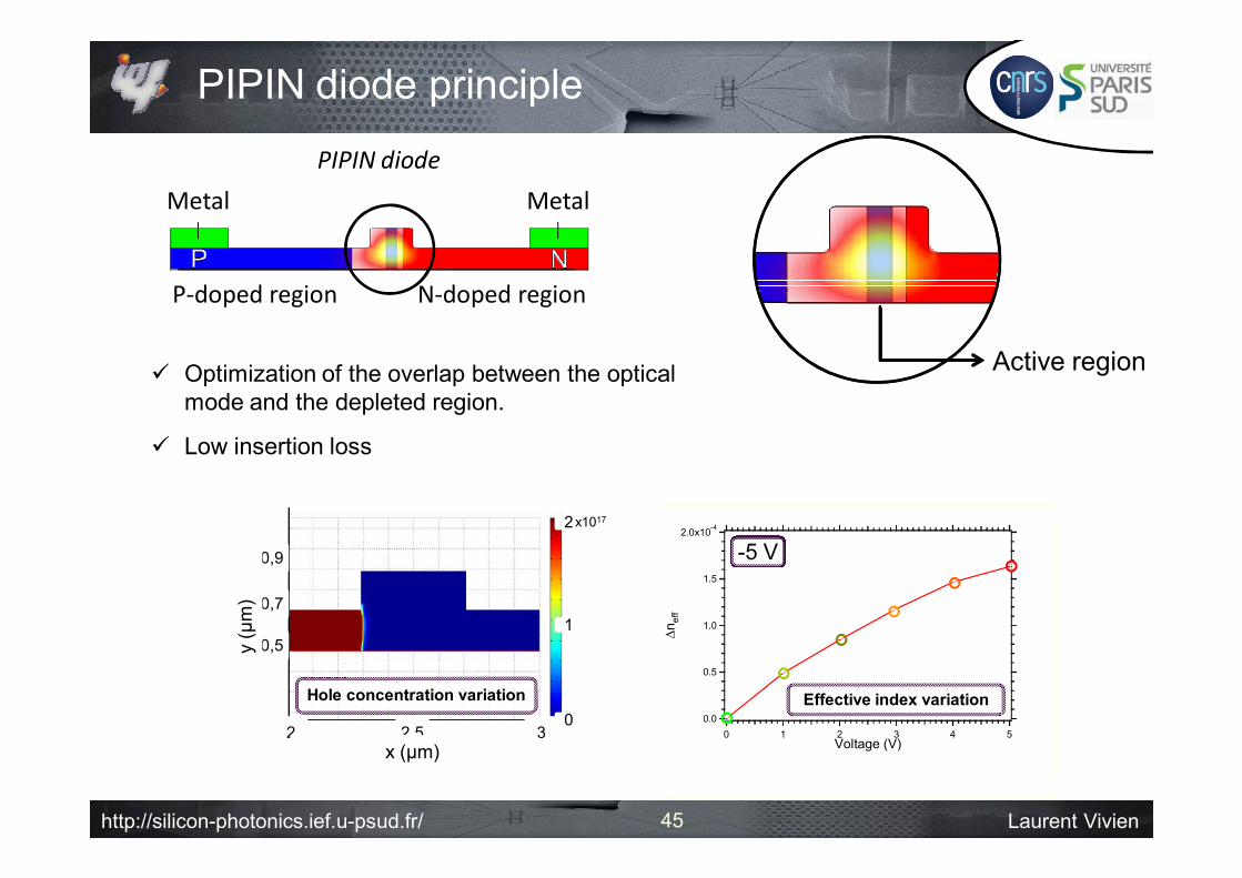
PIPIN diode principle
Hole concentration variation Refractive index variation
32,52
0,5
0,7
0,9
x (µm)
X10-48
4
032,52
0,5
0,7
0,9
x (µm)
x10172
1
0
y (µ
m)
2.0x10⁻⁴
1.5
1.0
0.5
0.0
nef
f
543210Voltage (V)
0 V
Effective index variation
-1 V-2 V-3 V-4 V-5 V
P‐doped region N‐doped region
PIPIN diodeMetal Metal
45
Active region Optimization of the overlap between the optical mode and the depleted region.
Low insertion loss
http://silicon-photonics.ief.u-psud.fr/ Laurent Vivien
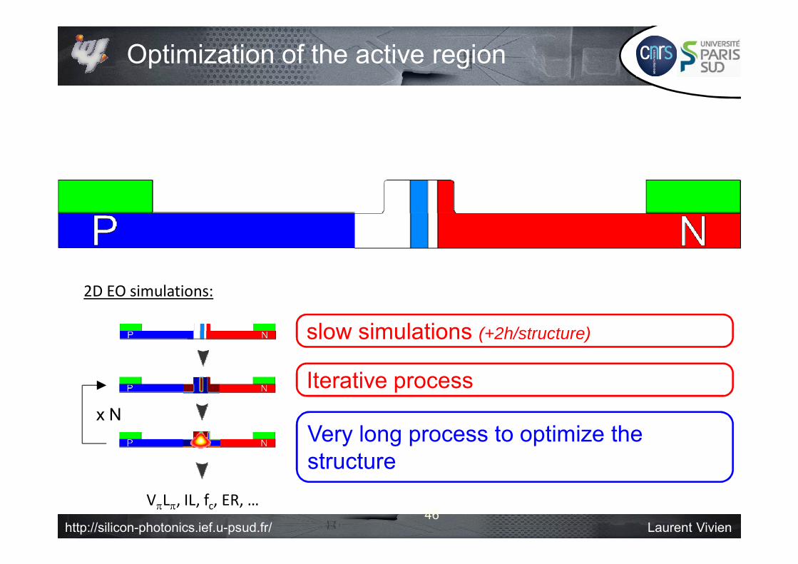
Electrical simulations
Structure design
Optical simulations
2D EO simulations:
slow simulations (+2h/structure)
Iterative process
Very long process to optimize the structure
Optimization of the active region
46
x N
VL, IL, fc, ER, …
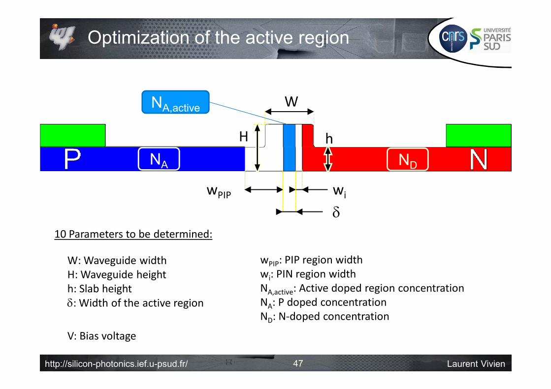
http://silicon-photonics.ief.u-psud.fr/ Laurent Vivien
W: Waveguide widthH: Waveguide heighth: Slab height: Width of the active region
W
H hNA ND
NA,active
10 Parameters to be determined:
wiwPIP
wiwPIP
Optimization of the active region
wPIP: PIP region widthwi: PIN region widthNA,active: Active doped region concentrationNA: P doped concentrationND: N‐doped concentration
V: Bias voltage
47
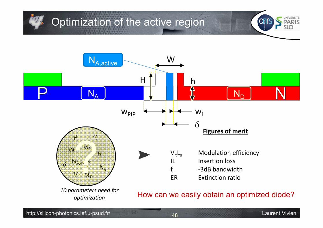
http://silicon-photonics.ief.u-psud.fr/ Laurent Vivien
W
H hNA ND
NA,active
wiwPIP
wiwPIP
VL Modulation efficiencyIL Insertion lossfc ‐3dB bandwidthER Extinction ratio
Figures of merit
10 parameters need for optimization
?
Optimization of the active region
48
How can we easily obtain an optimized diode?
http://silicon-photonics.ief.u-psud.fr/ Laurent Vivien
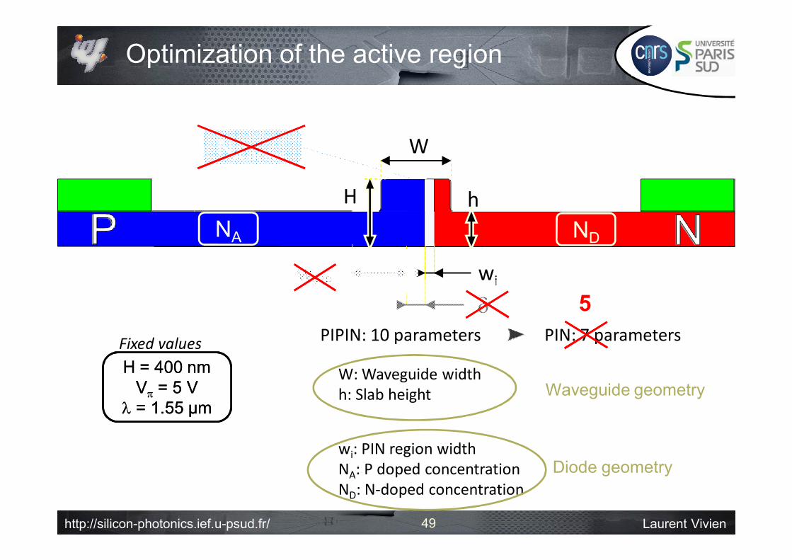
H hNA ND
NA,active
H = 400 nmV = 5 V
= 1.55 µm
H = 400 nmV = 5 V
= 1.55 µm
Fixed values PIPIN: 10 parameters PIN: 7 parameters
Optimization of the active region
wiwPIP
wiwPIP
W
5
W: Waveguide widthh: Slab height
wi: PIN region widthNA: P doped concentrationND: N‐doped concentration
Waveguide geometry
Diode geometry
49
http://silicon-photonics.ief.u-psud.fr/ Laurent Vivien
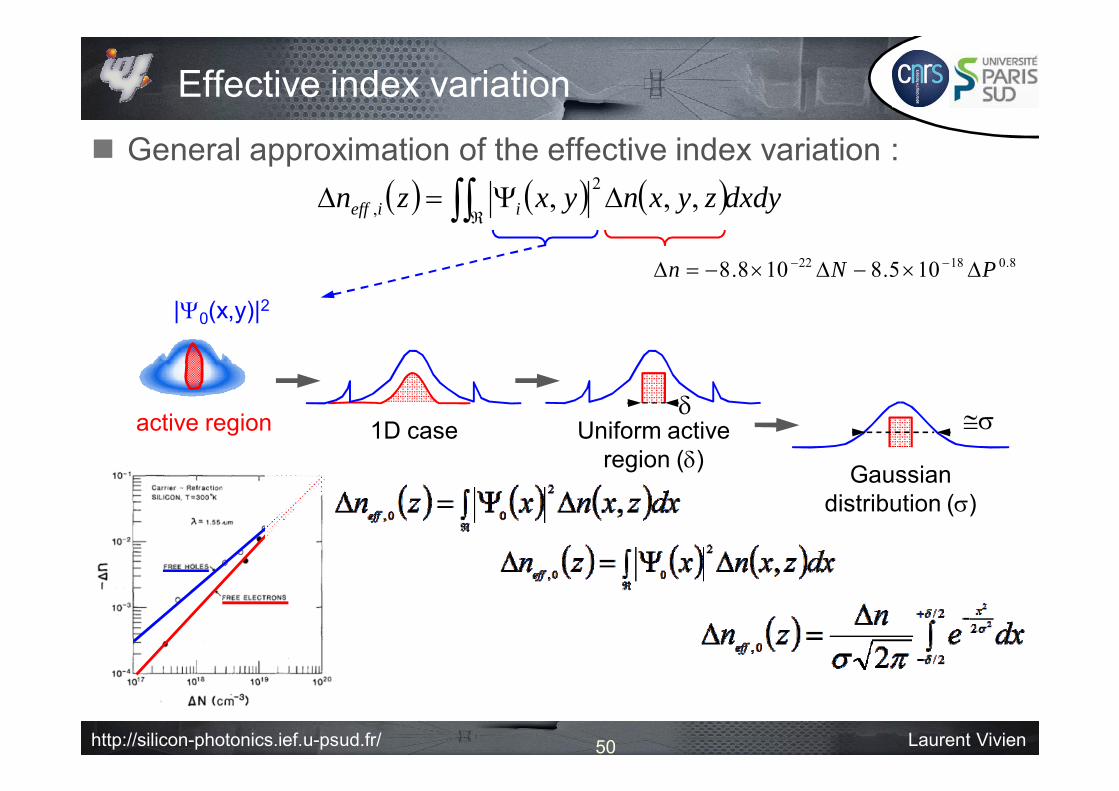
Effective index variation
General approximation of the effective index variation : dxdyzyxnyxzn iieff ,,, 2
,
|0(x,y)|2
active region 1D case
Uniform active region () Gaussian
distribution ()
8.01822 105.8108.8 PNn
50
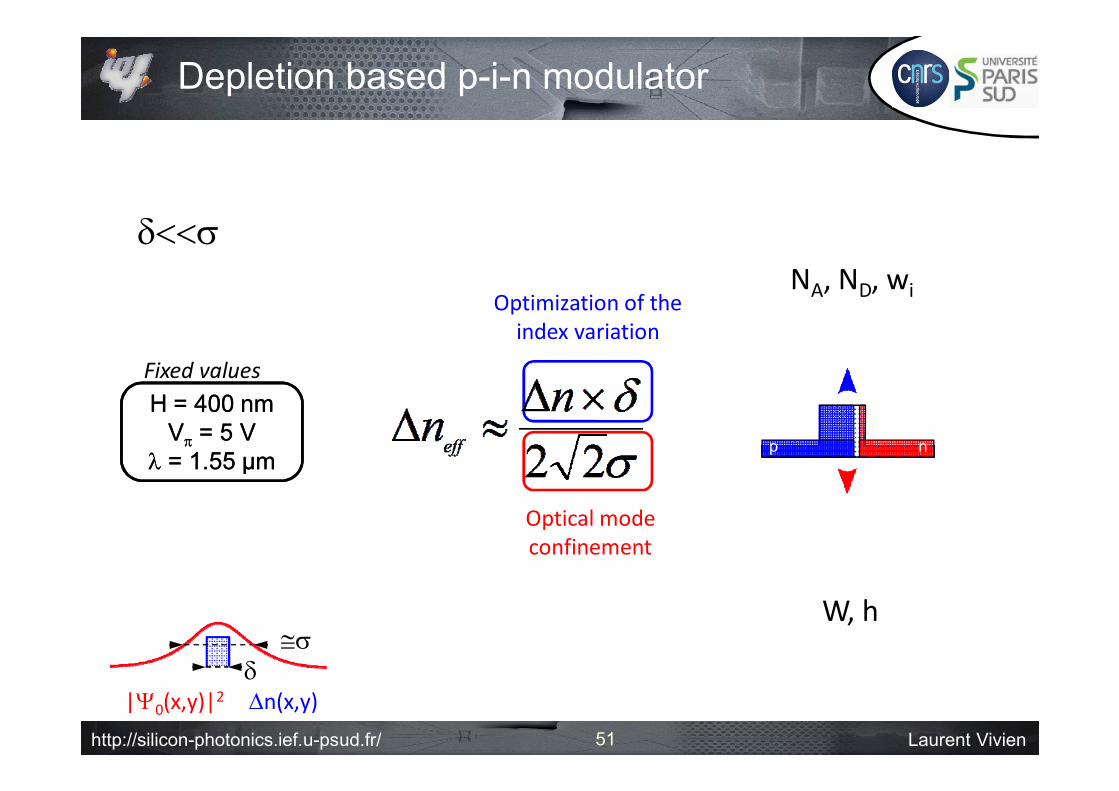
http://silicon-photonics.ief.u-psud.fr/ Laurent Vivien
Depletion based p-i-n modulator
51
Optical mode confinement
Optimization of the index variation
p np n
NA, ND, wi
W, h
n(x,y)|0(x,y)|2
H = 400 nmV = 5 V
= 1.55 µm
H = 400 nmV = 5 V
= 1.55 µm
Fixed values
http://silicon-photonics.ief.u-psud.fr/ Laurent Vivien
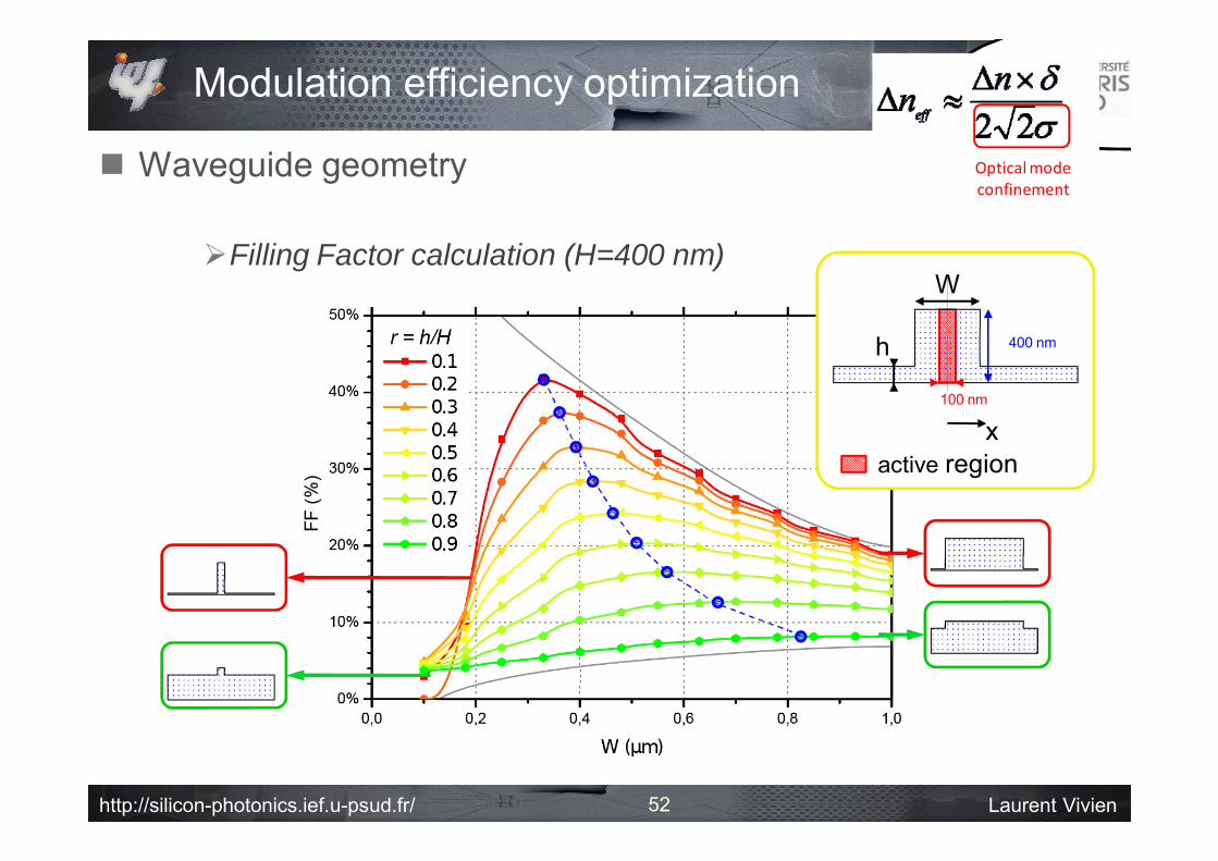
Modulation efficiency optimization
Waveguide geometry
Filling Factor calculation (H=400 nm)
100 nm
x
W
h 400 nm
active region
52
Optical mode confinement
http://silicon-photonics.ief.u-psud.fr/ Laurent Vivien
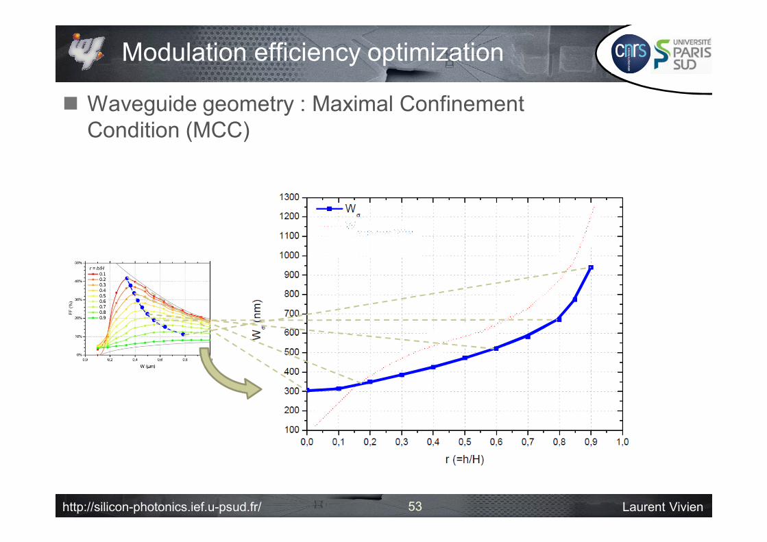
Modulation efficiency optimization
Waveguide geometry : Maximal Confinement Condition (MCC)
53

http://silicon-photonics.ief.u-psud.fr/ Laurent Vivien
Modulation efficiency optimization
Waveguide geometry : Single Mode TE/TM Condition (SMC)
multimode
single mode
54
http://silicon-photonics.ief.u-psud.fr/ Laurent Vivien
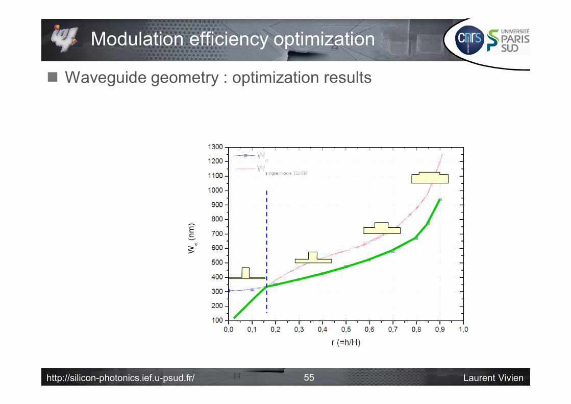
Modulation efficiency optimization
Waveguide geometry : optimization results
55

http://silicon-photonics.ief.u-psud.fr/ Laurent Vivien
Modulation efficiency optimization
22
nneff
Junction optimization
p n
56
NA, ND, wi

http://silicon-photonics.ief.u-psud.fr/ Laurent Vivien
Modulation efficiency optimization
Electrical model for the p-i-n junction
Evolution of the space charge region :
Active region width: n and p
2112ib
DAZCE wVV
NNqVw
V
0 V
x
-xp(0V) xn(0V)-xp(V) xn(V)x'
p n
y
VxVx pnpnpn 0,,,
Si n-doped p-doped
p
p
n
n
57
http://silicon-photonics.ief.u-psud.fr/ Laurent Vivien
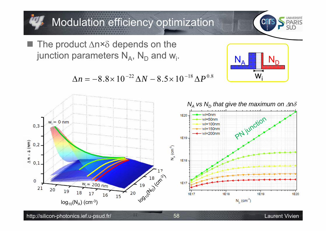
log10(NA) (cm-3)
Modulation efficiency optimization
The product n× depends on the junction parameters NA, ND and wi. NA ND
wi
NA vs ND that give the maximum on n
8.01822 105.8108.8 PNn
58
http://silicon-photonics.ief.u-psud.fr/ Laurent Vivien
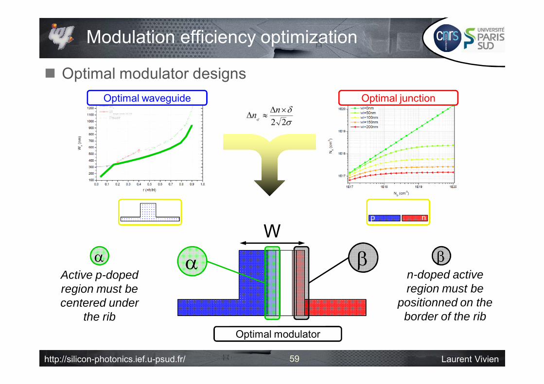
Optimal modulator
Modulation efficiency optimization
Optimal modulator designs
W
Active p-doped region must be centered under
the rib
n-doped active region must be
positionned on the border of the rib
Optimal waveguide
p n
Optimal junction
59
http://silicon-photonics.ief.u-psud.fr/ Laurent Vivien
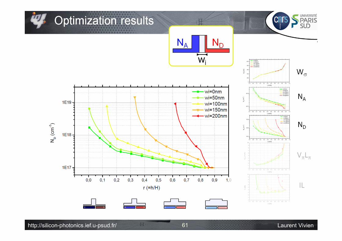
http://silicon-photonics.ief.u-psud.fr/ Laurent Vivien61
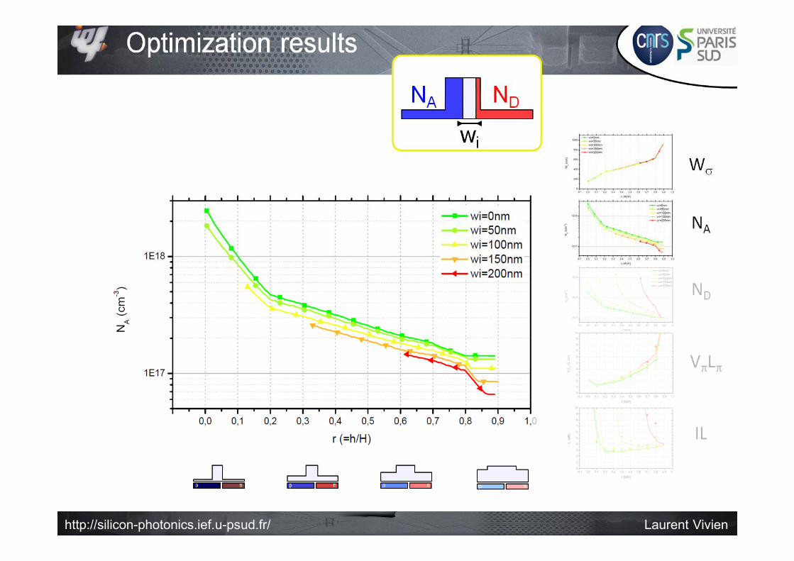
Optimization results
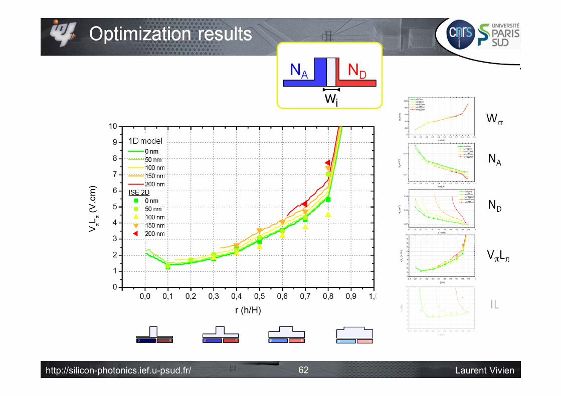
http://silicon-photonics.ief.u-psud.fr/ Laurent Vivien62
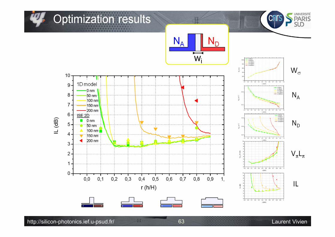
http://silicon-photonics.ief.u-psud.fr/ Laurent Vivien63

http://silicon-photonics.ief.u-psud.fr/ Laurent Vivien64
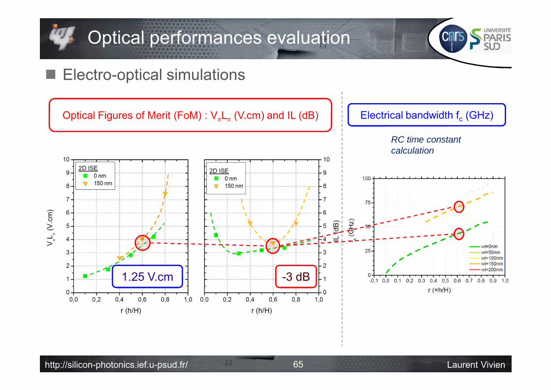
http://silicon-photonics.ief.u-psud.fr/ Laurent Vivien
-3 dB1.25 V.cm
Optical performances evaluation
Electro-optical simulations
Optical Figures of Merit (FoM) : VL (V.cm) and IL (dB) Electrical bandwidth fc (GHz)
RC time constant calculation
65
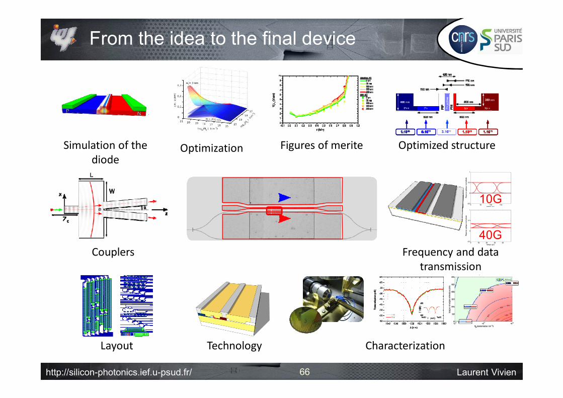
http://silicon-photonics.ief.u-psud.fr/ Laurent Vivien66
Simulation of the diode
Optimization Figures of merite Optimized structure
Couplers Frequency and data transmission
10G
40G
TechnologyLayout Characterization
From the idea to the final device
http://silicon-photonics.ief.u-psud.fr/ Laurent Vivien
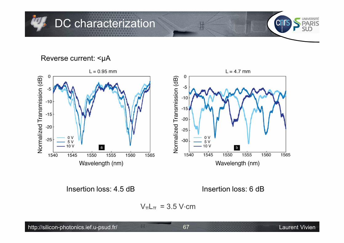
DC characterization
67
Reverse current: <µA
Insertion loss: 4.5 dB Insertion loss: 6 dB
VπLπ = 3.5 V⋅cm

http://silicon-photonics.ief.u-psud.fr/ Laurent Vivien
RF characteristics
68
40Gbit/sL = 4.7 mm
Extinction ratio: 6.6 dB
Insertion loss: 6 dB
http://silicon-photonics.ief.u-psud.fr/ Laurent Vivien
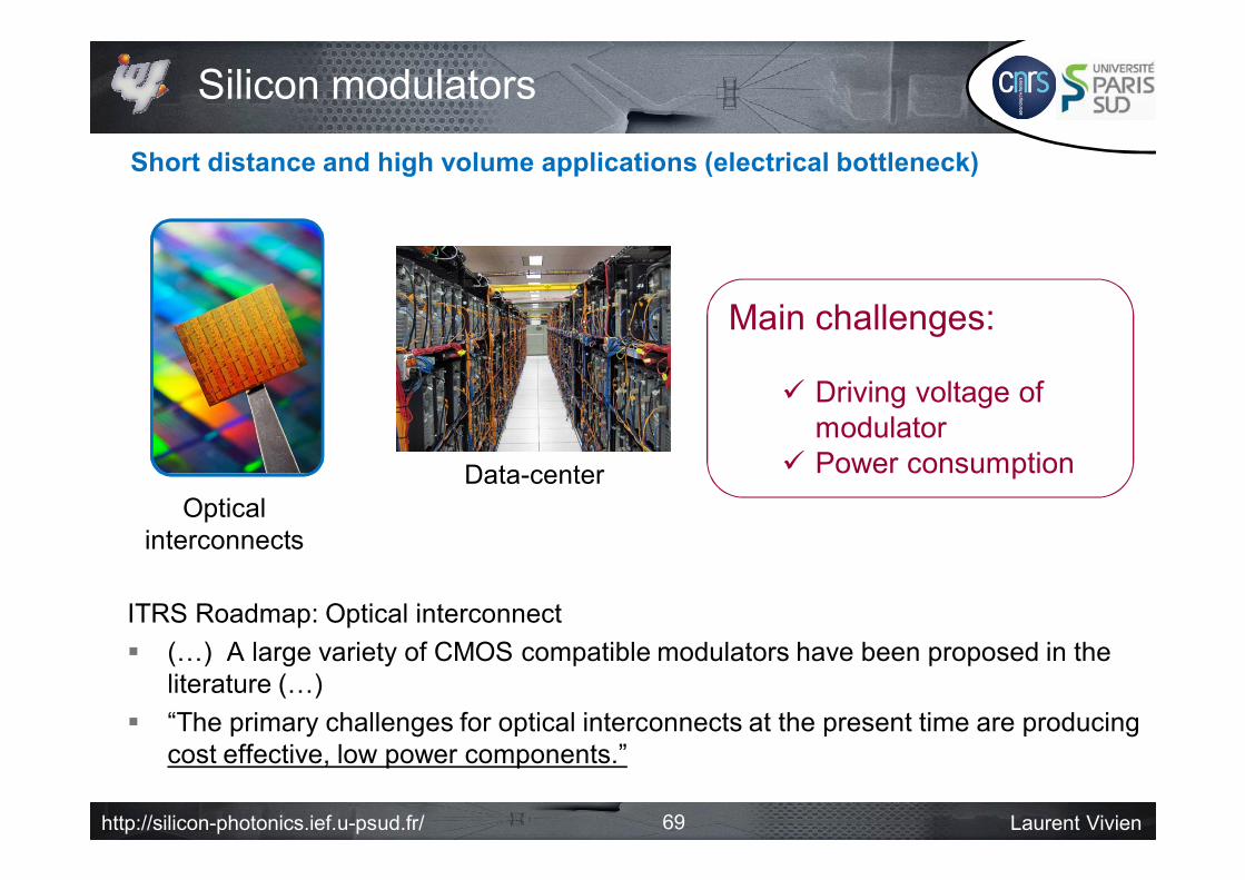
Silicon modulators
Data-center
Short distance and high volume applications (electrical bottleneck)
ITRS Roadmap: Optical interconnect (…) A large variety of CMOS compatible modulators have been proposed in the
literature (…) “The primary challenges for optical interconnects at the present time are producing
cost effective, low power components.”
Optical interconnects
69
Main challenges:
Driving voltage of modulator
Power consumption
http://silicon-photonics.ief.u-psud.fr/ Laurent Vivien
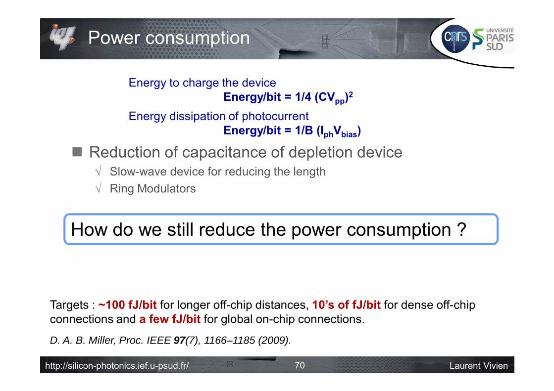
Power consumption
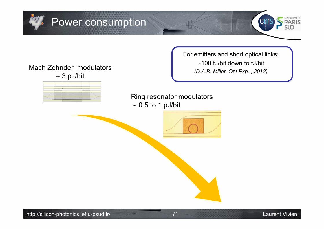
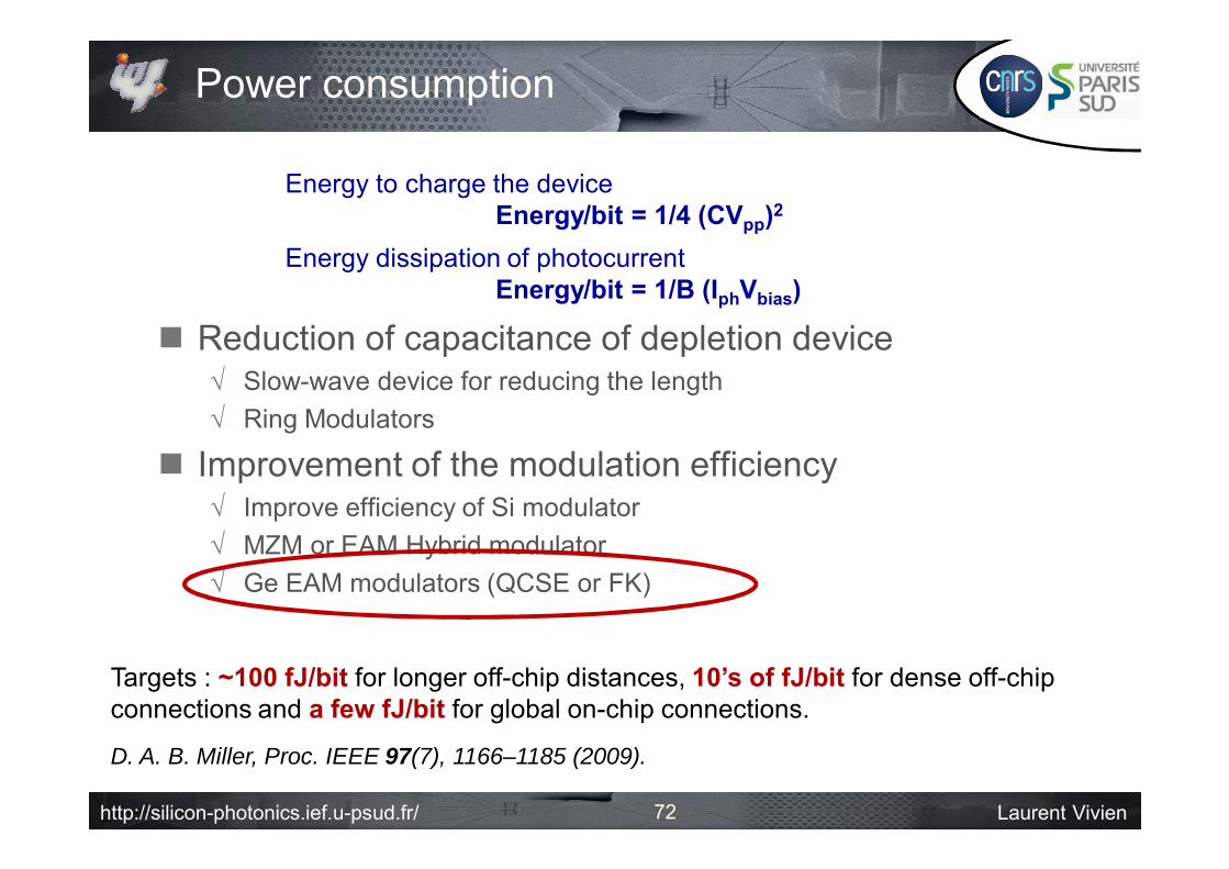
Reduction of capacitance of depletion device Slow-wave device for reducing the length Ring Modulators
Targets : ~100 fJ/bit for longer off-chip distances, 10’s of fJ/bit for dense off-chip connections and a few fJ/bit for global on-chip connections.
D. A. B. Miller, Proc. IEEE 97(7), 1166–1185 (2009).
Energy to charge the deviceEnergy/bit = 1/4 (CVpp)2
Energy dissipation of photocurrentEnergy/bit = 1/B (IphVbias)
How do we still reduce the power consumption ?
70
http://silicon-photonics.ief.u-psud.fr/ Laurent Vivien
Mach Zehnder modulators 3 pJ/bit
Ring resonator modulators 0.5 to 1 pJ/bit
Power consumption
For emitters and short optical links:~100 fJ/bit down to fJ/bit
(D.A.B. Miller, Opt Exp. , 2012)
71
http://silicon-photonics.ief.u-psud.fr/ Laurent Vivien
Power consumption
Reduction of capacitance of depletion device Slow-wave device for reducing the length Ring Modulators
Improvement of the modulation efficiency Improve efficiency of Si modulator MZM or EAM Hybrid modulator Ge EAM modulators (QCSE or FK)
Targets : ~100 fJ/bit for longer off-chip distances, 10’s of fJ/bit for dense off-chip connections and a few fJ/bit for global on-chip connections.
D. A. B. Miller, Proc. IEEE 97(7), 1166–1185 (2009).
Energy to charge the deviceEnergy/bit = 1/4 (CVpp)2
Energy dissipation of photocurrentEnergy/bit = 1/B (IphVbias)
72
http://silicon-photonics.ief.u-psud.fr/ Laurent Vivien
Gap
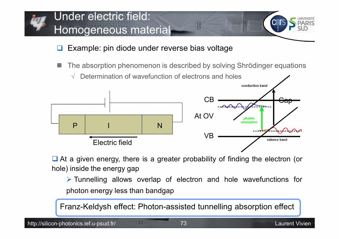
Under electric field: Homogeneous material
The absorption phenomenon is described by solving Shrödinger equations Determination of wavefunction of electrons and holes
Example: pin diode under reverse bias voltage
P NI
At a given energy, there is a greater probability of finding the electron (orhole) inside the energy gap
Tunnelling allows overlap of electron and hole wavefunctions forphoton energy less than bandgap
Franz-Keldysh effect: Photon-assisted tunnelling absorption effect
Electric field
CB
VB
At OV
73
http://silicon-photonics.ief.u-psud.fr/ Laurent Vivien
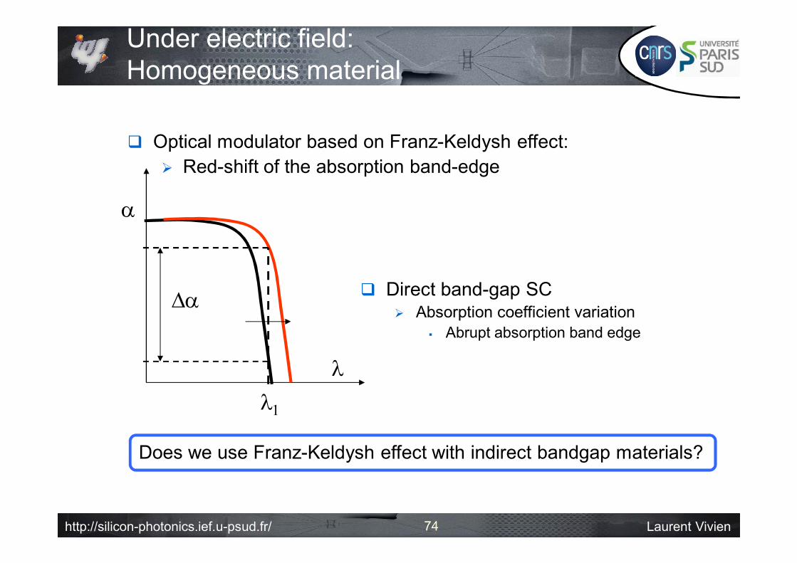
Optical modulator based on Franz-Keldysh effect: Red-shift of the absorption band-edge
Direct band-gap SC Absorption coefficient variation
Abrupt absorption band edge
Under electric field: Homogeneous material
Does we use Franz-Keldysh effect with indirect bandgap materials?
74
http://silicon-photonics.ief.u-psud.fr/ Laurent Vivien
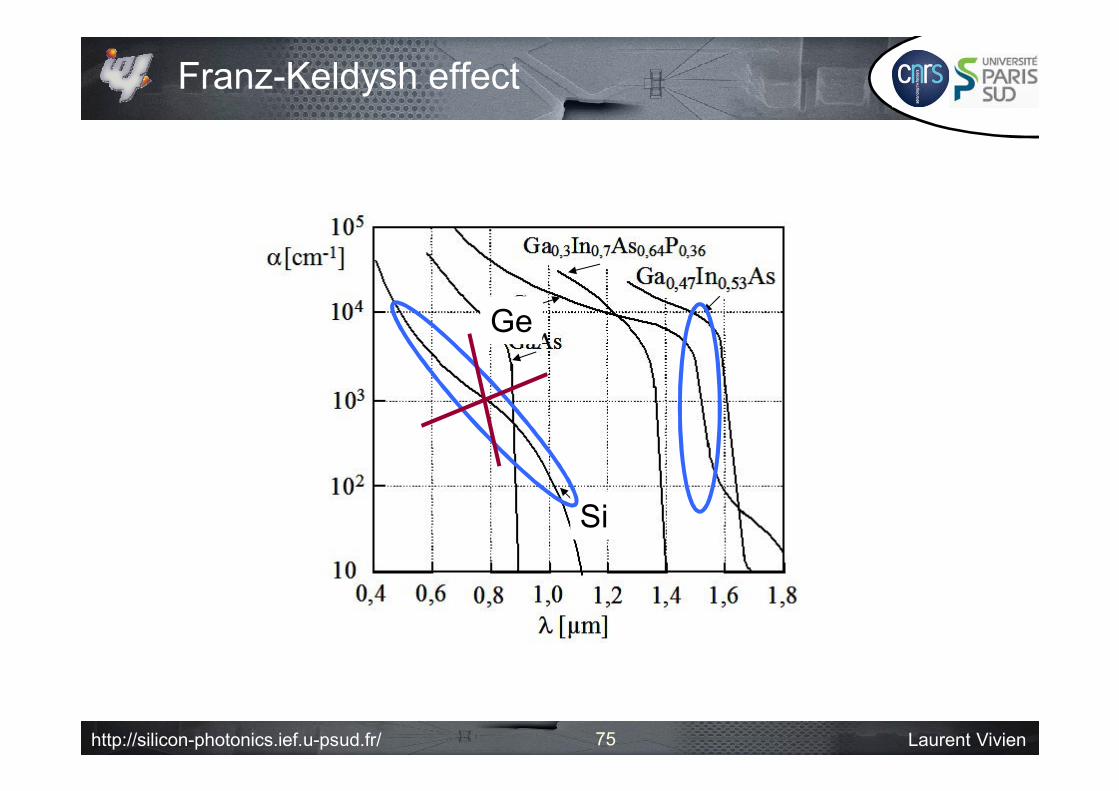
Franz-Keldysh effect
Ge
Si
75
http://silicon-photonics.ief.u-psud.fr/ Laurent Vivien
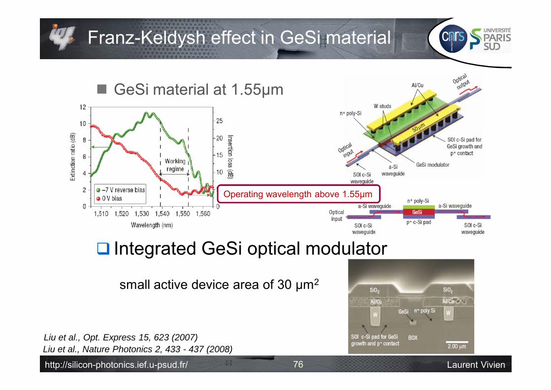
Franz-Keldysh effect in GeSi material
GeSi material at 1.55µm
Integrated GeSi optical modulator
Liu et al., Nature Photonics 2, 433 - 437 (2008)Liu et al., Opt. Express 15, 623 (2007)
small active device area of 30 µm2
76
Operating wavelength above 1.55µm

http://silicon-photonics.ief.u-psud.fr/ Laurent Vivien
Quantum well structures:
Heterostructures formed by a thin layer of a narrower-gap semiconductor between thicker layers of a wider-gap material lead to the formation of a potential well for both electrons and holes. Possible transition between
discrete energy level for electrons
Material 1
Mat
eria
l 2
E0
CB
VB
Ex : GaAlAs / GaAs/GaAlAs
Absorption effect in Quantum Well strucutres
Material 1
77
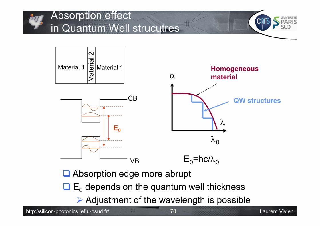
http://silicon-photonics.ief.u-psud.fr/ Laurent Vivien
E0=hc/0
Homogeneous material
QW structures
0
Material 1
Mat
eria
l 2
E0
CB
VB
Material 1
Absorption effect in Quantum Well strucutres
Absorption edge more abrupt E0 depends on the quantum well thickness Adjustment of the wavelength is possible
78
http://silicon-photonics.ief.u-psud.fr/ Laurent Vivien
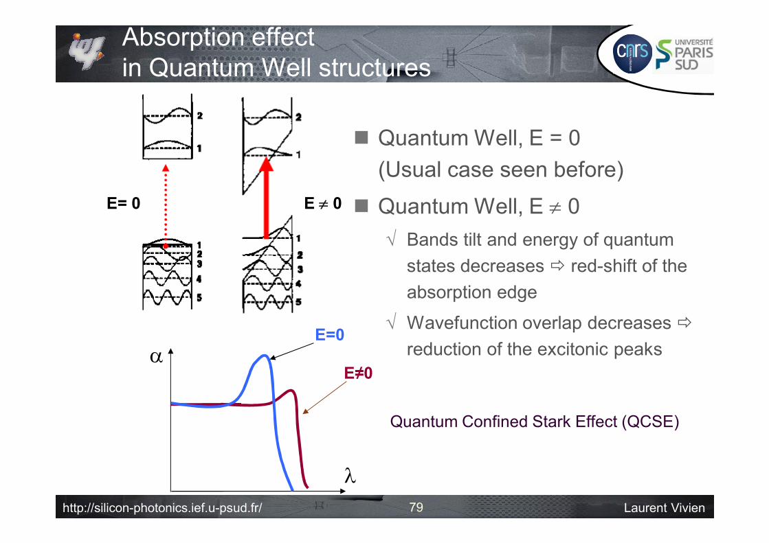
Absorption effect in Quantum Well structures
E=0
E≠0
E= 0
Quantum Well, E = 0(Usual case seen before)
Quantum Well, E 0 Bands tilt and energy of quantum
states decreases red-shift of the absorption edge
Wavefunction overlap decreases reduction of the excitonic peaks
E 0
Quantum Confined Stark Effect (QCSE)
79

http://silicon-photonics.ief.u-psud.fr/ Laurent Vivien
Active region design and growth
80
4.2% lattice mismatch between Si and Ge
QW structure: 10 nm Ge well/ 15 nm Si0.15Ge0.85 barrier
Strain-compensated structure
Average Ge in MQWs = 90% => Si0.1Ge0.9 bufferSi0.15Ge0.85
15 nmGe
10 nmSi0.15Ge0.85
15 nmSi0.1Ge0.9 relaxed buffer
SiGe p-type
SiGe n-type
SiGe spacer
SiGe spacer
QWs
Si(100)
Graded buffer from Si to Si0.1Ge0.9
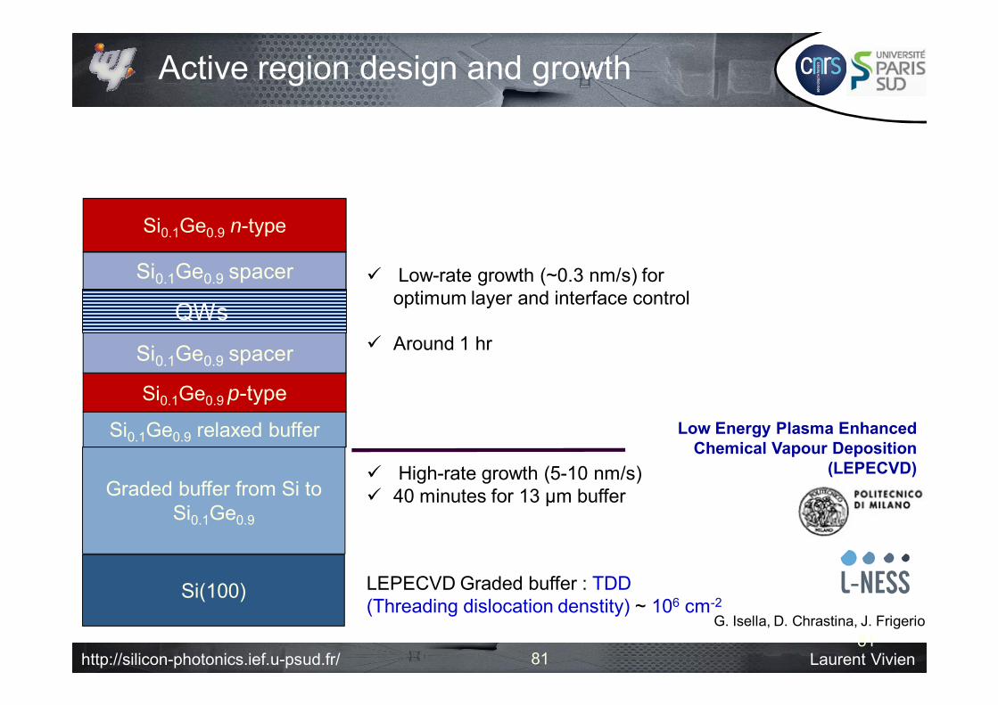
http://silicon-photonics.ief.u-psud.fr/ Laurent Vivien
G. Isella, D. Chrastina, J. Frigerio
Low Energy Plasma Enhanced Chemical Vapour Deposition
(LEPECVD)
Active region design and growth
81
LEPECVD Graded buffer : TDD (Threading dislocation denstity) ~ 106 cm-2
Low-rate growth (~0.3 nm/s) for optimum layer and interface control
Around 1 hr
High-rate growth (5-10 nm/s) 40 minutes for 13 µm buffer
Si0.15Ge0.8515 nm
Ge10 nm
Si0.15Ge0.8515 nmSi0.1Ge0.9 relaxed buffer
Si0.1Ge0.9 p-type
Si0.1Ge0.9 n-type
Si0.1Ge0.9 spacer
Si0.1Ge0.9 spacer
QWs
Si(100)
Graded buffer from Si to Si0.1Ge0.9
81
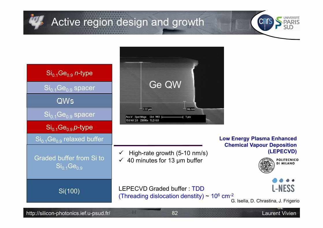
http://silicon-photonics.ief.u-psud.fr/ Laurent Vivien
G. Isella, D. Chrastina, J. Frigerio
Low Energy Plasma Enhanced Chemical Vapour Deposition
(LEPECVD)
Active region design and growth
82
LEPECVD Graded buffer : TDD (Threading dislocation denstity) ~ 106 cm-2
High-rate growth (5-10 nm/s) 40 minutes for 13 µm buffer
Ge QWGe QW
Si0.15Ge0.8515 nm
Ge10 nm
Si0.15Ge0.8515 nmSi0.1Ge0.9 relaxed buffer
Si0.1Ge0.9 p-type
Si0.1Ge0.9 n-type
Si0.1Ge0.9 spacer
Si0.1Ge0.9 spacer
QWs
Si(100)
Graded buffer from Si to Si0.1Ge0.9
82
http://silicon-photonics.ief.u-psud.fr/ Laurent Vivien
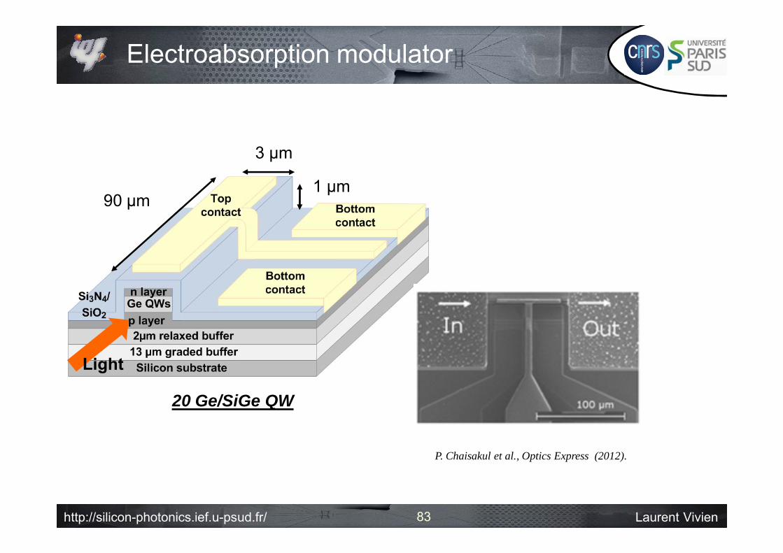
Electroabsorption modulator
3 µm
90 µm
Light
P. Chaisakul et al., Optics Express (2012).
1 µm
20 Ge/SiGe QW
83
http://silicon-photonics.ief.u-psud.fr/ Laurent Vivien
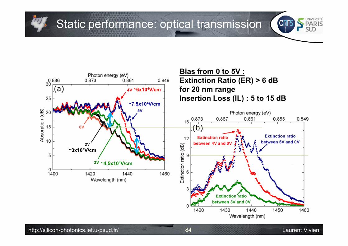
Static performance: optical transmission
~7.5x10⁴V/cm
~6x10⁴V/cm
~4.5x10⁴V/cm
~3x10⁴V/cm
Bias from 0 to 5V :Extinction Ratio (ER) > 6 dB for 20 nm rangeInsertion Loss (IL) : 5 to 15 dB
84
http://silicon-photonics.ief.u-psud.fr/ Laurent Vivien85
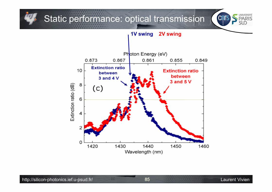
Static performance: optical transmission
85
1V swing 2V swing
http://silicon-photonics.ief.u-psud.fr/ Laurent Vivien
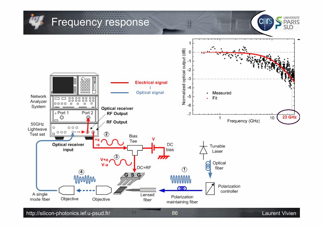
Frequency response
86
http://silicon-photonics.ief.u-psud.fr/ Laurent Vivien
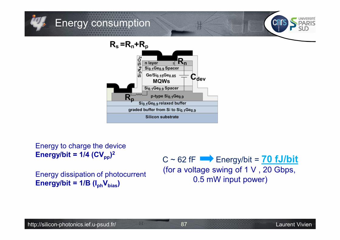
Energy to charge the deviceEnergy/bit = 1/4 (CVpp)2
Energy consumption
Energy dissipation of photocurrentEnergy/bit = 1/B (IphVbias)
87
C ~ 62 fF Energy/bit = 70 fJ/bit (for a voltage swing of 1 V , 20 Gbps,
0.5 mW input power)
http://silicon-photonics.ief.u-psud.fr/ Laurent Vivien
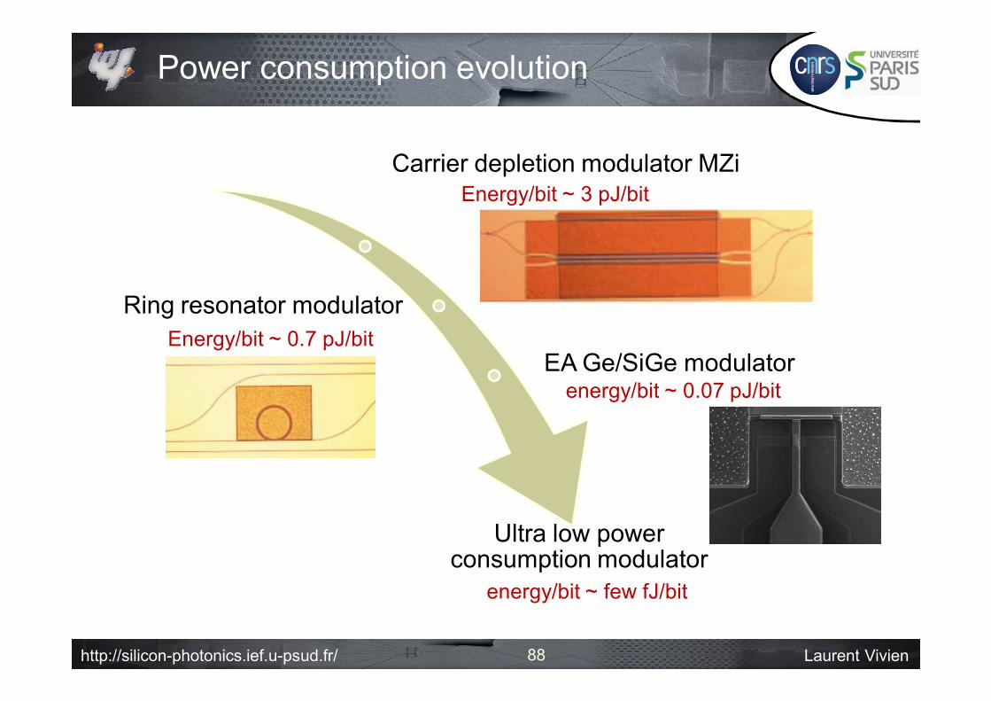
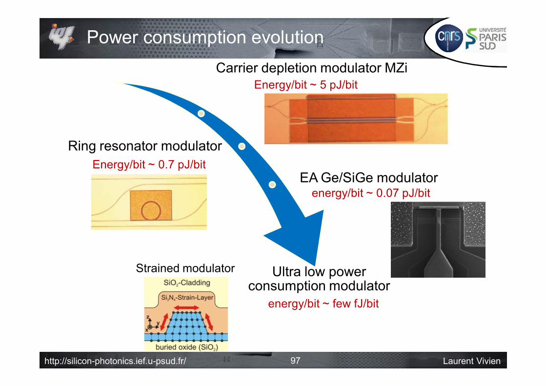
Power consumption evolution
88
Carrier depletion modulator MZi
Ring resonator modulator
EA Ge/SiGe modulator
Ultra low power consumption modulator
Energy/bit ~ 3 pJ/bit
Energy/bit ~ 0.7 pJ/bit
energy/bit ~ 0.07 pJ/bit
energy/bit ~ few fJ/bit
http://silicon-photonics.ief.u-psud.fr/ Laurent Vivien89
What do absorption variation also induce ?
….
Interesting for optical modulation
Electro-refraction
http://silicon-photonics.ief.u-psud.fr/ Laurent Vivien
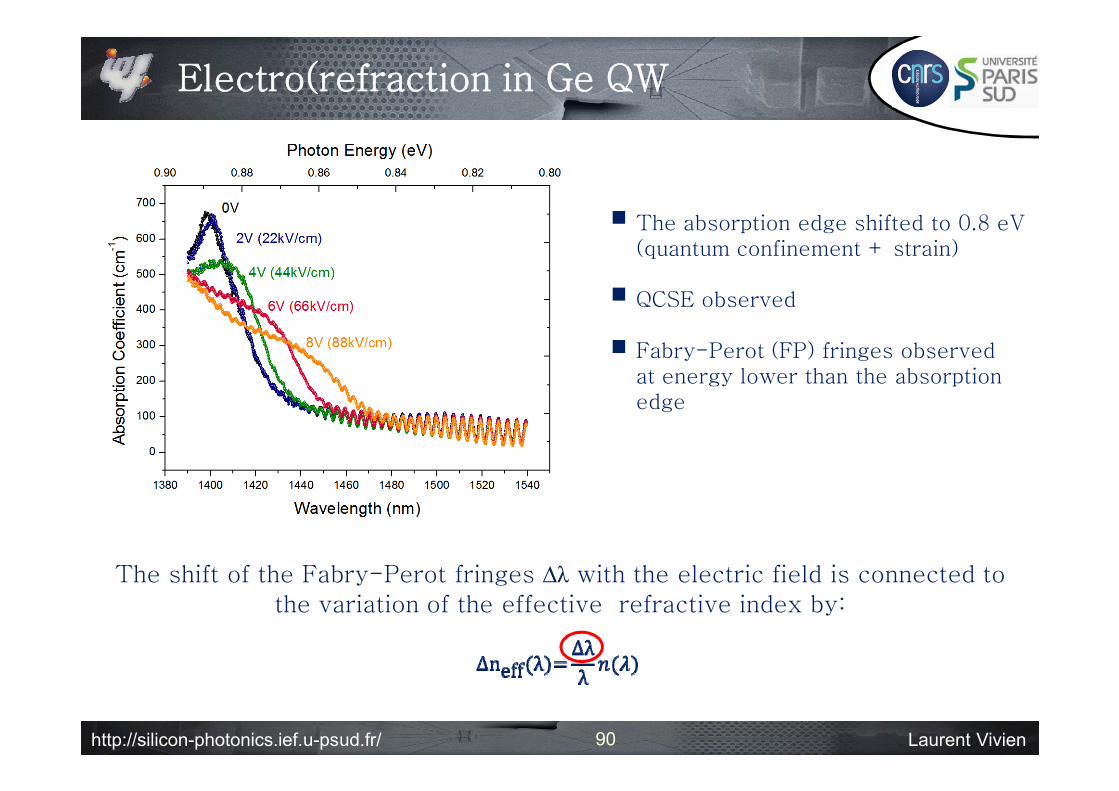
The absorption edge shifted to 0.8 eV(quantum confinement + strain)
QCSE observed
Fabry-Perot (FP) fringes observedat energy lower than the absorptionedge
Electro(refraction in Ge QW
90
Silicon Substrate (DSP)
The shift of the Fabry-Perot fringes ∆λ with the electric field is connected to the variation of the effective refractive index by:
TE polarization

http://silicon-photonics.ief.u-psud.fr/ Laurent Vivien91
The absorption edge shifted to 0.8 eV(quantum confinement + strain)
QCSE observed
Fabry-Perot (FP) fringes observedat energy lower than the absorptionedge
Electro(refraction in Ge QW
91
Silicon Substrate (DSP)
The shift of the Fabry-Perot fringes ∆λ with the electric field is connected to the variation of the effective refractive index by:
TE polarization
http://silicon-photonics.ief.u-psud.fr/ Laurent Vivien92
Electro(refraction in Ge QW
92
Silicon Substrate (DSP)
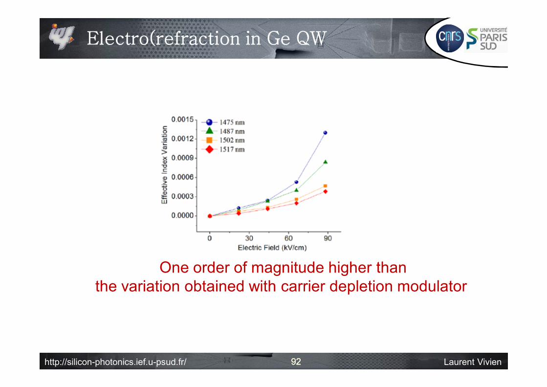
One order of magnitude higher thanthe variation obtained with carrier depletion modulator

http://silicon-photonics.ief.u-psud.fr/ Laurent Vivien
Ge/SiGe MQW phase-shifter
93
GaAs/AlGaAs MQW 0.55 Vcm J.S. Sites et al. J. Lightwave Technol. 12, 1167 (1992)
figure of merit VπLπ of 0.46 Vcm (88kV/cm, 1475 nm)
0.4 VcmInAlGaAs MQW on Si system
H.-W. Chen et al., IEEE 20, 1920 (2008)

http://silicon-photonics.ief.u-psud.fr/ Laurent Vivien
Si0.15Ge0.8515 nm
Ge10 nm
Si0.15Ge0.8515 nm
2 µm Si0.1Ge0.9 relaxed buffer
doped-P Si0.1Ge0.9
doped-N Si0.1Ge0.9
Si0.1Ge0.9
Si0.1Ge0.9
QWs
Si
13 µm thick gradual buffer from Si to Si0.1Ge0.9
Schematic description
Challenge: coupling the light from silicon to Ge/SiGe QW
Si
13 µm thick gradual buffer from Si to Si0.1Ge0.9
The real scale
2 µm Si0.1Ge0.9 relaxed buffer
Integrated circuits based onGe/SiGe QW ?
94

http://silicon-photonics.ief.u-psud.fr/ Laurent Vivien
1st option: waveguide in the relaxed SiGe layer (thanks to the graded buffer )
Si0.15Ge0.8515 nm
Ge10 nm
Si0.15Ge0.8515 nm
1.5 µm Si0.16Ge0.84 relaxed buffer
doped-N Si0.09Ge0.91
doped-N Si0.09Ge0.91
Si0.09Ge0.91
Si0.09Ge0.91
QWs
Si
8 µm thick gradual buffer from Si to Si0.1Ge0.83
Ge concentration in the waveguide: trade-off between • Strain compensation• Optical loss
Optical loss of each device, including input/output coupling with Si0.16Ge0.84waveguide < 5dB
Integration on bulk silicon
95
P. Chaisakul et al, accepted to Nature Photonics
http://silicon-photonics.ief.u-psud.fr/ Laurent Vivien
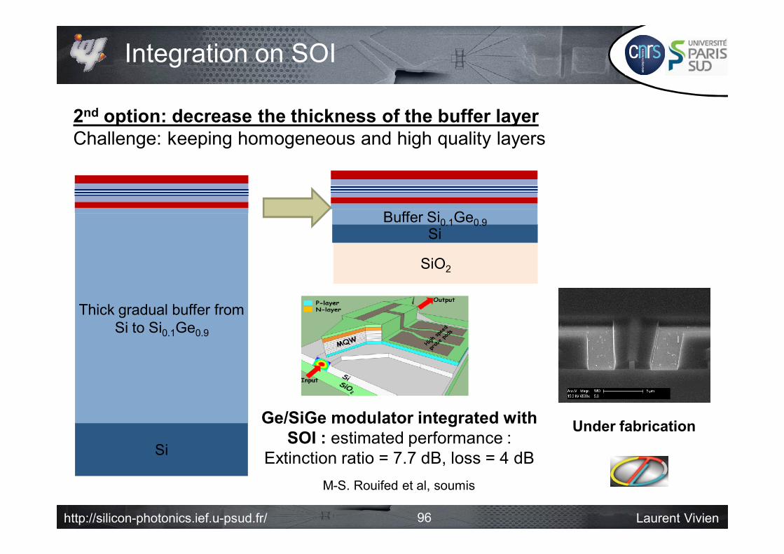
2nd option: decrease the thickness of the buffer layerChallenge: keeping homogeneous and high quality layers
Si
Thick gradual buffer from Si to Si0.1Ge0.9
SiO2
SiBuffer Si0.1Ge0.9
Ge/SiGe modulator integrated with SOI : estimated performance :
Extinction ratio = 7.7 dB, loss = 4 dB
Under fabrication
M-S. Rouifed et al, soumis
Integration on SOI
96
http://silicon-photonics.ief.u-psud.fr/ Laurent Vivien
Power consumption evolutionCarrier depletion modulator MZi
Ring resonator modulator
EA Ge/SiGe modulator
Ultra low power consumption modulator
Energy/bit ~ 5 pJ/bit
Energy/bit ~ 0.7 pJ/bit
energy/bit ~ 0.07 pJ/bit
energy/bit ~ few fJ/bit
Strained modulator
97
http://silicon-photonics.ief.u-psud.fr/ Laurent Vivien
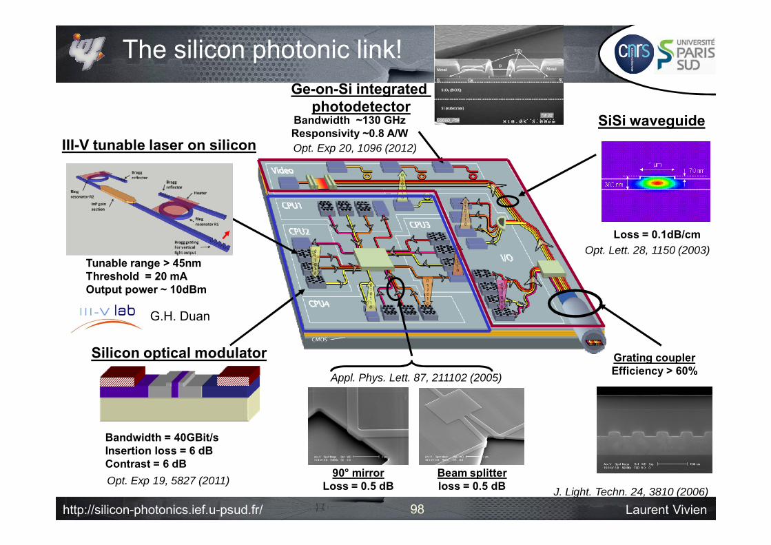
The silicon photonic link!
SiSi waveguide
Ge-on-Si integrated photodetector
Silicon optical modulator
Loss = 0.1dB/cm
Beam splitterloss = 0.5 dB
90° mirrorLoss = 0.5 dB
Opt. Lett. 28, 1150 (2003)
Appl. Phys. Lett. 87, 211102 (2005)
Grating couplerEfficiency > 60%
J. Light. Techn. 24, 3810 (2006)
III-V tunable laser on silicon
Bandwidth = 40GBit/sInsertion loss = 6 dBContrast = 6 dBOpt. Exp 19, 5827 (2011)
Bandwidth ~130 GHzResponsivity ~0.8 A/WOpt. Exp 20, 1096 (2012)
G.H. Duan
Tunable range > 45nmThreshold = 20 mAOutput power ~ 10dBm
98