Silicon photonics: Waveguide modulators and...
64
2572-11 Winter College on Optics: Fundamentals of Photonics - Theory, Devices and Applications Laurent Vivien 10 - 21 February 2014 Institut dElectronique Fondamentale CNRS UMR 8622 Université Paris Sud, 91405 Orsay Cedex France Silicon photonics: Waveguide modulators and detectors
Transcript of Silicon photonics: Waveguide modulators and...

2572-11
Winter College on Optics: Fundamentals of Photonics - Theory, Devices and Applications
Laurent Vivien
10 - 21 February 2014
Institut d�Electronique Fondamentale CNRS UMR 8622
Université Paris Sud, 91405 Orsay Cedex France
Silicon photonics: Waveguide modulators and detectors

Silicon PhotonicsSilicon-based micro and nanophotonic devices
http://silicon-photonics.ief.u-psud.fr/ 1
Waveguide modulators and detectors
Laurent VivienInstitut d’Electronique Fondamentale, CNRS UMR 8622,
Université Paris Sud, 91405 Orsay Cedex, France
http://silicon-photonics.ief.u-psud.fr/
Silicon photonics:

Silicon PhotonicsSilicon-based micro and nanophotonic devices
http://silicon-photonics.ief.u-psud.fr/ 2
Silicon photonics:Waveguide modulators and detectors
L. Vivien,
D. Marris-Morini, G. Rasigade, L. Virot, M. Ziebell, D. Perez-Galacho, P. Chaisakul, M-S. Rouifed, P. Crozat, P. Damas, E. Cassan
D. Bouville, S. Edmond, X. Le RouxInstitut d’Electronique Fondamentale, CNRS UMR 8622,
Université Paris Sud, 91405 Orsay Cedex, Francehttp://silicon-photonics.ief.u-psud.fr/
J-M. Fédéli, S, Olivier, Jean Michel Hartmann
CEA-LETI, Minatec 17 rue des Martyrs, 38054 Grenoble cedex 9, France
G. Isella, D. Chrastina, J. FrigerioL-NESS, Politecnico di Milano, Polo di Como, Via Anzani 42, I-22100 Como, Italy
C. Baudot, F. BoeufSTMicroelectronics, Silicon Technology Development, Crolles, France

http://silicon-photonics.ief.u-psud.fr/ Laurent Vivien3
The Institute for Fundamental Electronics
135 CNRS researchers,professors and lecturers,technical staff
+100 PhD students, Post-Docand visitors
~ 400 students undergoingtraining within IEF's ground
University Technology Center(CTU) MINERVE
IEF is a joint research unit between CNRS and University of Paris Sud
Spintronics and Si-based Nano-electronics
Micro-Nano systems and systems
Photonics

http://silicon-photonics.ief.u-psud.fr/ Laurent Vivien4
University Technology Center
University Technology Centre (1000 m²):
Photolithography: 2-sided UV lithography with wafer bonding Deep UV lithography (248 nm) 2 e-beams (Raith150 and 100keV nanobeam) Laser
Etching:Wet etching (KOH, TMAH, …) Dry etching :
fluoride gases RIE (2 systems) ICP Si deep etching IBE 02 plasma etching Chloride gases RIE
…
IEF-MINERVE member of The French Network on “Basic Technological Research” (RTB)

http://silicon-photonics.ief.u-psud.fr/ Laurent Vivien5
Silicon photonics group
Optical modulatorsAll siliconNL materialsPlasmon
Strained Si photonics
Carbon nanotubes for photonics
Passive devicesGrating couplersWaveguidesSplittersOptical DistributionMulti-wavelength circuits
CEA / LETI
Photonic crystalsSlow lightSuperprismNL enhancement
Ge detectorsSurface illuminatedIntegratedAPD
Bottom contact
Top contact
Ge 3 µm
CEA / LETI
40 GBit/s
300 nm300 nm
Ge-SiGe QW photonics Source Modulator detector Ge QWGe QW
4 permanent Researchers 2 engineers, technicians 16 PhD students 2 post-doc 2-4 master students / year
Pockels effect

http://silicon-photonics.ief.u-psud.fr/ Laurent Vivien6
Outline
Motivation (Pavel’s and Lorenzo’s talks)
Photodetectors on silicon Main characteristics Results
Optical modulators Figures of Merit Modulation in silicon Results
Conclusion

Data centers
Optical telecommunications
Environment
Interconnects
Chemical/Biological sensors
Free space communications
FTTH
Military
Silicon photonics

http://silicon-photonics.ief.u-psud.fr/ Laurent Vivien
Silicon photonic building blocksOn‐chip III‐V laser on Si
Laser Modulator Detector
Emitter Receiver
Inputwaveguide
RF electrodes
10 µm
Modulator
photodetector
Off‐chip III‐V laser
Optical coupler
Germanium‐based laser
8

http://silicon-photonics.ief.u-psud.fr/ Laurent Vivien9
Photodetection

http://silicon-photonics.ief.u-psud.fr/ Laurent Vivien10
Basic principle
e-
e-
h+
h+
h
- +
Main characteristic of the material?

http://silicon-photonics.ief.u-psud.fr/ Laurent Vivien11
Basic principle
The aborption of photons generates electron-hole pairs Photogenerated carriers are then collected thanks to an
external field Photocurrent
e-
e-
h+
h+
h
- +

http://silicon-photonics.ief.u-psud.fr/ Laurent Vivien12
Absorption mechanisms (II)
Direct gap SC (III-V SC)
k
Ek
h
k
Ek
hPhonon
absorption
Phonon emission
Indirect gap SC (IV-IV SC)
G
EG=hc/G
G
absorbed photons generate free electron-hole pairs

http://silicon-photonics.ief.u-psud.fr/ Laurent Vivien13
Material choice Wavelength ranges:
1.3 µm – 1.6 µm 0.85 µm
Direct bandgap

http://silicon-photonics.ief.u-psud.fr/ Laurent Vivien14
Indirect bandgap
Material choice
Wavelength ranges: 1.3 µm – 1.6 µm 0.85 µm

http://silicon-photonics.ief.u-psud.fr/ Laurent Vivien15
Indirect bandgap
Direct gap absorption
Material choice
Two choices: InGaAs or Ge
Wavelength ranges: 1.3 µm – 1.6 µm 0.85 µm
http://silicon-photonics.ief.u-psud.fr/ Laurent Vivien16
InGaAs versus Germanium
What is the best material for light detectionin near-IR wavelength range ?
Material choice

http://silicon-photonics.ief.u-psud.fr/ Laurent Vivien17
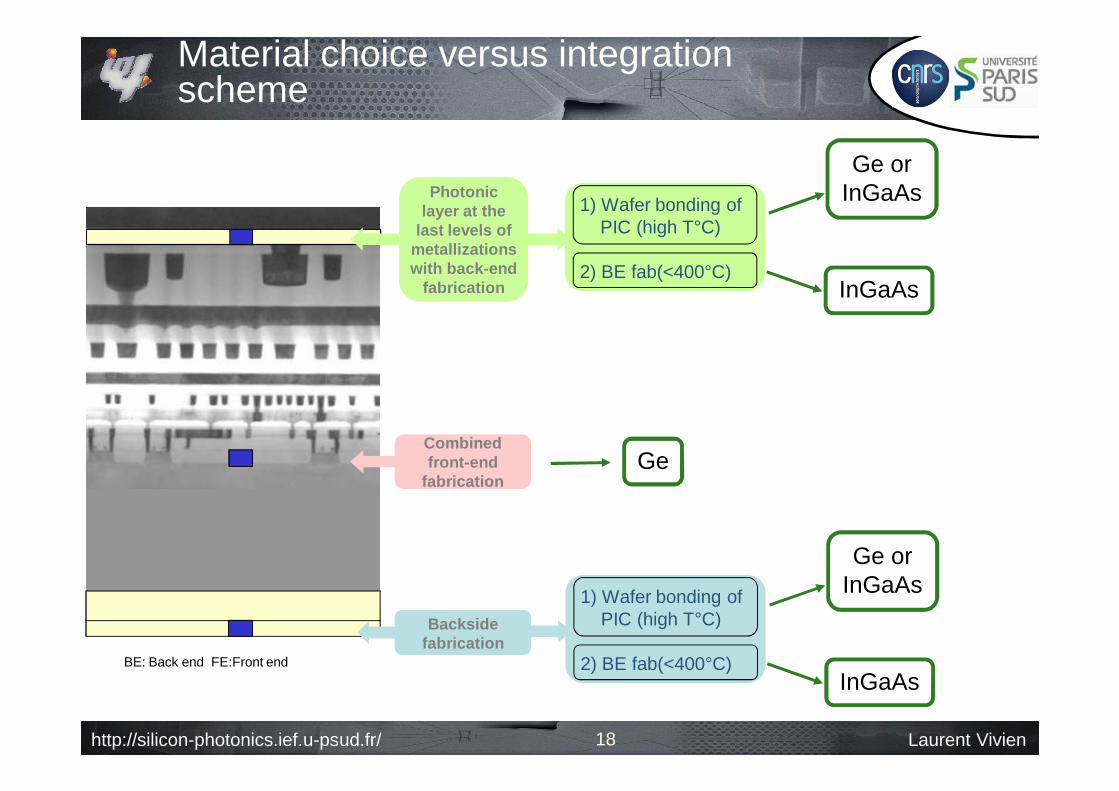
1) Wafer bonding ofPIC (high T°C)
2) BE fab(<400°C)
Combined front-end
fabrication
Photonic layer at the
last levels of metallizations with back-end
fabrication
Backside fabrication
•Through substrate connections•High integration density
•Specific FE CMOS technology and library•Flip-Chip hybridization of InP components•Moderate integration density•Efficient connections of EIC and PIC
•Use of standard FE CMOS technologies•High integration density (AboveIC)•Multilevel process capability
BE: Back end FE:Front end
1) Wafer bonding ofPIC (high T°C)
2) BE fab(<400°C)
Material choice versus electronic photonic integration scheme
http://silicon-photonics.ief.u-psud.fr/ Laurent Vivien
Material choice versus integration scheme
18
1) Wafer bonding ofPIC (high T°C)
2) BE fab(<400°C)
Ge orInGaAs
InGaAs
Combined front-end
fabrication
Photonic layer at the
last levels of metallizations with back-end
fabrication
Backside fabrication
BE: Back end FE:Front end
1) Wafer bonding ofPIC (high T°C)
2) BE fab(<400°C)
Ge orInGaAs
InGaAs
Ge

http://silicon-photonics.ief.u-psud.fr/ Laurent Vivien19
Are III-V materials integrated in silicon platform?
Monolithic integration via epitaxial growthNo viable solutions yet
Hybrid integrationBCB or molecular bonding

http://silicon-photonics.ief.u-psud.fr/ Laurent Vivien20
Exemple of hybrid integration
1. Sample preparation2. Sample cleaning + removal of cap layer3. BCB bonding and curing4. InP substrate removal5. Removal of sacrificial layers6. Detector mesa etching7. BCB insulation8. Opening of the contact windows9. Metallization10. Post-processing
III-V materials can be integrated on siliconWhat about wafer size and technology?

http://silicon-photonics.ief.u-psud.fr/ Laurent Vivien21
Germanium on silicon:Pros and Cons
Absorption coefficient of pure Ge:9000 cm-1 at =1.3µm LABS
95% 3.3µm (!) Low capacitance devices High frequency operation
High carrier mobility

http://silicon-photonics.ief.u-psud.fr/ Laurent Vivien
Crystal lattice structure of Silicon and Germanium
22
Si and Ge have a diamond lattice structure (two interdigitated FCC lattices)
Properties Silicon GermaniumLattice parameter:
a (Å) 5.431 5.658
Atomic density (cm-3) 5,0.1022 4,42.1022
Atom radius (Å) 0.117 0,122Lattice structure Diamond Diamond
Lattice parameter mismatch: ~4.2 %

http://silicon-photonics.ief.u-psud.fr/ Laurent Vivien23
Germanium on silicon:Pros and Cons
Lattice misfit with Si of about 4.2% specific growth strategies required (wafer-scale and localized)
Low indirect bandgap: EG=0.66eV high dark current for MSM devices
Absorption coefficient of pure Ge:9000 cm-1 at =1.3µm LABS
95% 3.3µm (!) Low capacitance devices High frequency operation
High carrier mobility
Can we directly growth Ge on silicon?

http://silicon-photonics.ief.u-psud.fr/ Laurent Vivien
The lattice mismatch
4.2% of lattice mismatch between germanium and silicon
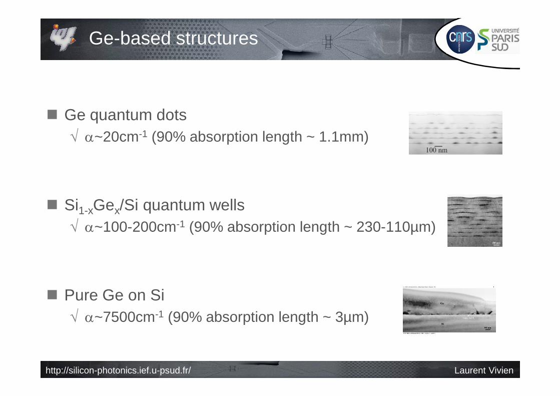
Ge quantum dots
Si1-xGex/Si quantum wells
Pure Ge on Si
SiGe on Si
QD, QW or Bulk ?
http://silicon-photonics.ief.u-psud.fr/ Laurent Vivien
Ge-based structures
Ge quantum dots ~20cm-1 (90% absorption length ~ 1.1mm)
Si1-xGex/Si quantum wells ~100-200cm-1 (90% absorption length ~ 230-110µm)
Pure Ge on Si ~7500cm-1 (90% absorption length ~ 3µm)

http://silicon-photonics.ief.u-psud.fr/ Laurent Vivien26
Ge growth strategies
Thick virtual SiGe substrates (10µm) Need for a new integration scheme – difficult to integrate with
SOI waveguides.
Si(100)
SiGe buffer graded from Si to Ge
Ge

http://silicon-photonics.ief.u-psud.fr/ Laurent Vivien27
Ge growth strategies
Thick virtual SiGe substrates (10µm) Need for a new integration scheme – difficult to integrate with
SOI waveguides.
Growth on thin SiGe buffers The thickness of the thin SiGe buffer is around 1µmAlways too thick for integration with SOI
Si(100)
SiGe buffer graded from Si to Ge
Ge

http://silicon-photonics.ief.u-psud.fr/ Laurent Vivien28
Ge growth strategies
Thick virtual SiGe substrates (10µm) Need for a new integration scheme – difficult to integrate with
SOI waveguides.
Growth on thin SiGe buffers The thickness of the thin SiGe buffer is around 1µmAlways too thick for integration with SOI
Direct Ge growth on Si
Si(100)
Ge

http://silicon-photonics.ief.u-psud.fr/ Laurent Vivien
Germanium growth
29
Two-step growth process: Direct growth of Ge on Si using a low temperature (350°) CVD
process thin (a few 10nm) highly-dislocated Ge layer
Growth of a thick Ge layer (a few 100nm) at a higher temperature (600°) high quality Ge absorbing layer
Thermal annealing to reduce the dislocation density
Si substrate (001)
LT Ge (350°C, 50nm)
HT Ge (600°C,300-500nm) 400nm

http://silicon-photonics.ief.u-psud.fr/ Laurent Vivien30
Epitaxial growth techniques
Molecular beam epitaxy (MBE) Solid sources evaporated gas sputtering on the wafer Ultra-high vacuum required (P10-10 Torr) Low thermal budgets (T<550°C) High-control of layer and multi-layer thicknesses (<nm) Low growth rates (<1 nm/min)
Chemical Vapor Deposition (CVD): High-control of layer and multi-layer thicknesses (<nm) Proper for large wafer-scale fabrication A large variety of CVD techniques have been developed, depending on the pressure
and heating systems:• Ultra-High Vacuum CVD (UHV-CVD)• Reduced-pressure CVD (RP-CVD)• Low-energy plasma-enhanced CVD (LEPE-CVD)

http://silicon-photonics.ief.u-psud.fr/ Laurent Vivien31
Absorption of Ge-on-Si
The red-shift of the absorption edge is due to the tensile strain-induced bandgap narrowing within the Ge layer, resulting from the difference in the thermal expansion coefficients of Ge and Si
Strong absorption up to 1.6µm

http://silicon-photonics.ief.u-psud.fr/ Laurent Vivien
Photodetector characteristics
32
http://silicon-photonics.ief.u-psud.fr/ Laurent Vivien
Photodetector characterisitics: Quantum efficiency (I)
33
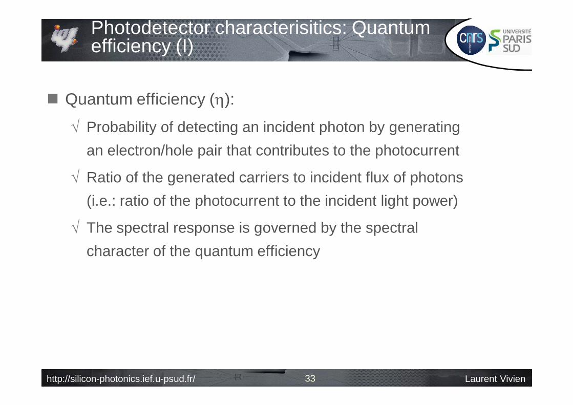
Quantum efficiency ():
Probability of detecting an incident photon by generating an electron/hole pair that contributes to the photocurrent
Ratio of the generated carriers to incident flux of photons (i.e.: ratio of the photocurrent to the incident light power)
The spectral response is governed by the spectral character of the quantum efficiency
http://silicon-photonics.ief.u-psud.fr/ Laurent Vivien
Photodetector characterisitics: Quantum efficiency (II)
34
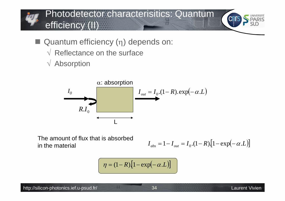
Quantum efficiency () depends on: Reflectance on the surface Absorption
L
: absorption I0
0.IR
LRIIout .exp).1.(0
LRIII outabs .exp1).1.(1 0 The amount of flux that is absorbedin the material
LR .exp1).1(

http://silicon-photonics.ief.u-psud.fr/ Laurent Vivien
Photodetector characterisitics:Responsivity
35
Responsivity () is often more useful to characterize the response of photodetectors
Responsivity is typically linear with wavelength but real photodetectors exhibit a deviation from the ideal behaviour due to photogenerated carrier trapping
24.1)(.
.
. µmhq
http://silicon-photonics.ief.u-psud.fr/ Laurent Vivien
Photodetector characterisitics:Response time (I)
36
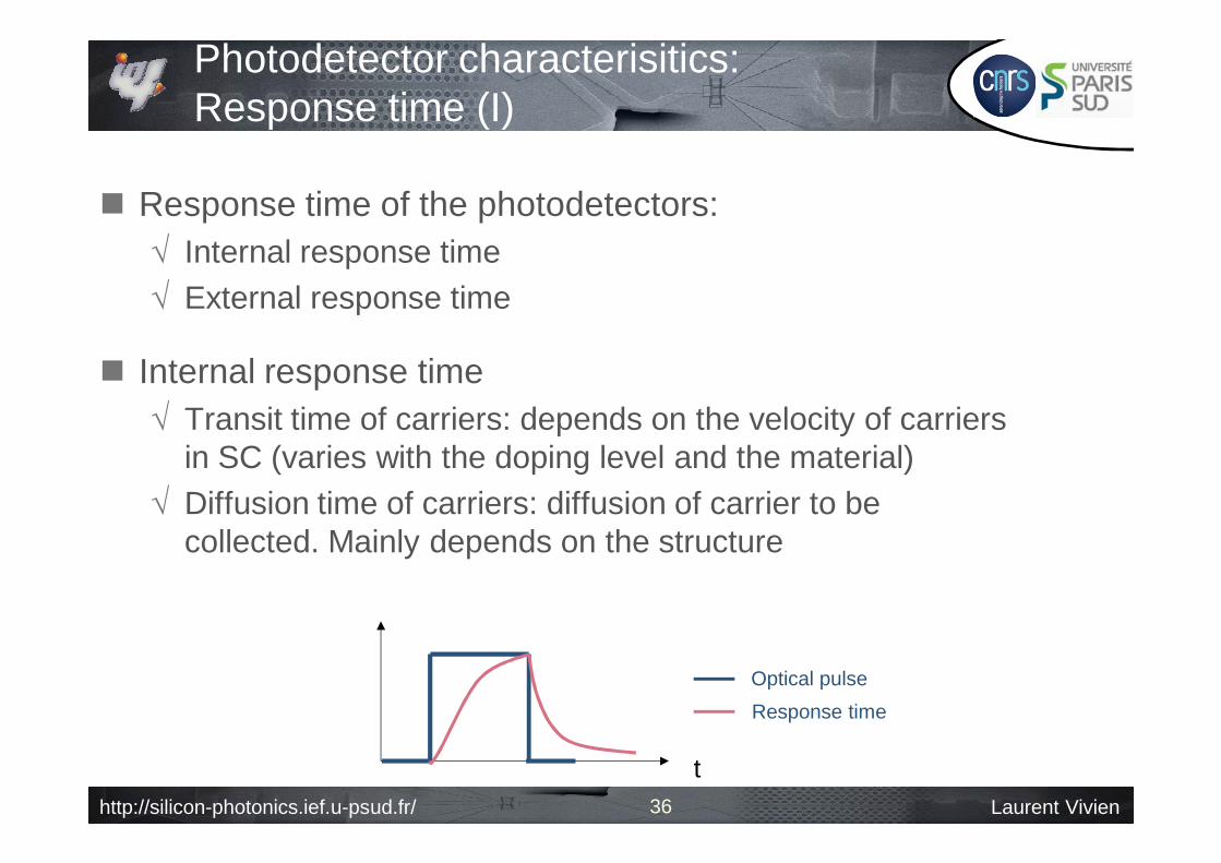
Response time of the photodetectors: Internal response time External response time
Internal response time Transit time of carriers: depends on the velocity of carriers
in SC (varies with the doping level and the material) Diffusion time of carriers: diffusion of carrier to be
collected. Mainly depends on the structure
t
Optical pulseResponse time

http://silicon-photonics.ief.u-psud.fr/ Laurent Vivien
Photodetector characterisitics:Response time (II)
37
External response time
Cd Cp
Rd
R1
R2
Cd: Diode capacitance
Cp: Parasitic capacitance
Rd: Diode resistance
R1: contact and substrateresistances
R2: charge resistancetypical schematic electrical circuit of the photodiode
R1 and Rd << R2
Response time = R2 (CP + Cd)
http://silicon-photonics.ief.u-psud.fr/ Laurent Vivien38
Photodetector specifications (I)
“Compatibility” with silicon technology Silicon-based materials will be better
Large wafer scale technology
Permit electronic integration (Transimpedance amplifier – TIA)
Low cost integration schemes
Broadband detection (1.3 -1.6 µm)
High absorption coefficient
Low dark current Electrical configuration of photodetectors,
Quality of the absorbing layer.

http://silicon-photonics.ief.u-psud.fr/ Laurent Vivien39
Photodetector specifications (II)
High bandwidth (frequency operation > 10 GHz)
Low carrier transit time,
Low RC constant – depend on the considered electrical structure (pin diode, MSM detector).
High responsivity Optimize the light interaction with absorbing layer.
Compactness
Strong absorption coefficient

http://silicon-photonics.ief.u-psud.fr/ Laurent Vivien40
Photodetector integration
Surface illuminated photodetectors
High bandwidth“Simple” process
“Low” responsivity
Two approaches
Responsivity ~0.1 A/W

http://silicon-photonics.ief.u-psud.fr/ Laurent Vivien41
Photodetector integration
Two approaches
Surface illuminated photodetectors
photodetectors integratedin waveguide
High bandwidth“Simple” process
“Low” responsivity
High bandwidthHigh responsivity
Optical coupling

http://silicon-photonics.ief.u-psud.fr/ Laurent Vivien
Integrated photodetectors:optical coupling
42
Single mode (TE)
SOI waveguides
Vertical coupling Butt coupling

http://silicon-photonics.ief.u-psud.fr/ Laurent Vivien
Vertical coupling
BEP 3D
FDTD 3D
95 % absorption length < 10 µm with 310nm germanium thickness
0
0.2
0.4
0.6
0.8
1
0 100 200 300 400 500 600
7 µm4 µm
10 µm
Abs
orbe
d op
tical
pow
erGermanium thickness (nm)
Length:
M. ROUVIÈRE, et al., Optical Engineering, 44 (2005) 183-187
0
0,2
0,4
0,6
0,8
1
0
20
40
60
80
100
0 2 4 6 8 10
Abso
rbed
pow
er (%
)
Absorbed power derivate (A
U)
Photodetector length (µm)A
bsorption power
SiGe

http://silicon-photonics.ief.u-psud.fr/ Laurent Vivien
Butt coupling
44
95% absorption length < 4µm
Negligible lateral divergence

http://silicon-photonics.ief.u-psud.fr/ Laurent Vivien
Ge Photodetectors
45
Europe: PSUD-IEF, CEA-Léti, Stuttgart Univ., Roma Univ. …Asia: Tokyo Univ., A*Star, Petra, AIST, Chinese Academy of Sciences, …North America: Intel, MIT, IBM, Cornell, Luxtera, Ligthwire, Kortura, Oracle …
http://silicon-photonics.ief.u-psud.fr/ Laurent Vivien46
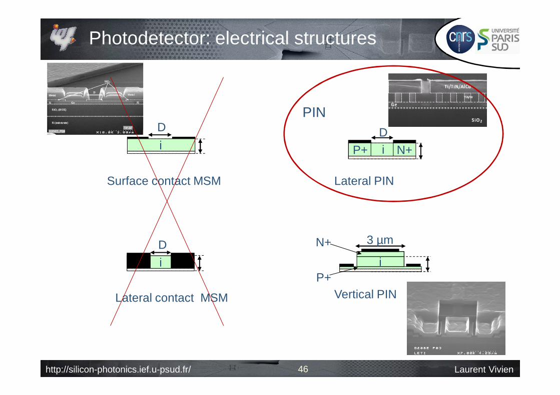
Photodetector: electrical structures
MSM PIN
Surface contact MSM
iD
iD
Lateral contact MSM
P+ N+iD
Lateral PIN
N+i
3 µm
Vertical PINP+

http://silicon-photonics.ief.u-psud.fr/ Laurent Vivien
Diode band structure
47

http://silicon-photonics.ief.u-psud.fr/ Laurent Vivien48
Diode band structure
48
Forward or reverse bias ?

http://silicon-photonics.ief.u-psud.fr/ Laurent Vivien
PIN Photodiodes : Design considerations
49
Junction disposition
Lateral PIN
Contact on Ge: only one etching step
Definition of intrinsic region by ion implantation
Wi
35 GHz50 GHz
70 GHz
3dB Bandwidth
R > 0.9 A/W
http://silicon-photonics.ief.u-psud.fr/ Laurent Vivien
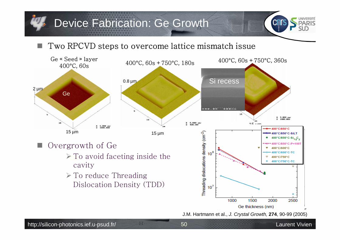
Device Fabrication: Ge Growth
Two RPCVD steps to overcome lattice mismatch issue
50
Ge
Ge
Ge
Ge « Seed » layer 400°C, 60s
2 µmGe
15 µm
-1000
-500
0
500
1000
0 5 10 15D
epth
(nm
)
X (µm)
60s @ 400°C + 360s @ 750°C
60s @ 400°C +180s @ 750°C
60s @ 400°C +60s @ 750°C
300s @ 400°C
60s @ 400°C
400°C, 60s +750°C, 360s
15 µm
2 µmSiO2
SiSiO2
Si recess
15 µm
400°C, 60s +750°C, 180s
0.8 µm
Overgrowth of Ge
To avoid faceting inside the cavity
To reduce Threading Dislocation Density (TDD)
J.M. Hartmann et al., J. Crystal Growth, 274, 90-99 (2005)

http://silicon-photonics.ief.u-psud.fr/ Laurent Vivien
Device Fabrication: Ge Growth
Post epitaxial thermal cycling to further reduce TDD in the Ge layer
CMP step to remove protruded Ge
SiO2 encapsulation
Ion implantation of Ge
N-type : Phosphorus
P-type : Boron
Rapid Thermal Anneal
Ge
Y. Yamamoto et al., Solid-State Electronics, 60-1, 2–6, (2011).
51

http://silicon-photonics.ief.u-psud.fr/ Laurent Vivien
Device Fabrication: Contact and Metal
Oxide encapsulation
Planarization
Contact definition
0.4x0.4µm vias for metal filling (TiN/W)
Ti/TiN/AlCu pad defined by etching
52
Inputwaveguide
RF electrodes
10 µm
Lateral

http://silicon-photonics.ief.u-psud.fr/ Laurent Vivien
Results : Dark current and responsivity
53
Dark current median, mean and best values (373 dies per wafer)Photodiodes Wi=0.5µm Wi=0.7µm Wi=1µm
Wafer 1 2 3 1 2 3 1 2 3
@-1VMedian (nA) 85 74 112 66 62 80 68 61 71Mean (nA) 433 105 1707 350 83 576 347 110 963Best (nA) 32 25 27 18 9.5 9 19 17 6
Yield 99.2% 99.7% 97.8% 100% 100% 99.7% 100% 100% 99.7%
Responsivity @ 1550nm under Zero bias
Wi=0.5µm 0.5A/W
Wi=0.7µm 0.6A/W
Wi=1µm 0.8A/W
Efficient carrier collection at zero bias due to strong built-in electric field
New run: dark current ~1nA @ -1V for Wi = 0.5µm
Measured responsivity lower than theoretical values

http://silicon-photonics.ief.u-psud.fr/ Laurent Vivien
Characterization methods:Bandwidth (I)
54
Femtosecond pulse experiments
0
0.2
0.4
0.6
0.8
1
0 40 80 120 160
Device Under TestAcquisition SystemConvolution
Pho
tovo
ltage
(UA)
Time (ps)
Response time (ps)
fs laser

http://silicon-photonics.ief.u-psud.fr/ Laurent Vivien
Characterization methods:Bandwidth (I)
55
Femtosecond pulse experiments
Opto-RF experiments with a Vector Network Analyzer
12 GHz
28 GHz
42 GHz
- 3 dB

http://silicon-photonics.ief.u-psud.fr/ Laurent Vivien
Characterization methods:Bandwidth (II)
56
Data transmission measurements
Eye diagram
Samplingoscilloscope
optical source
Bias T
Vpol
Optical fiber
RF cable
RF cable
optical modulator = 1.55 µm
PRBSgenerator
Pseudo Random Binary Sequence

http://silicon-photonics.ief.u-psud.fr/ Laurent Vivien
Results : Bandwidth measurement
Opto-electric frequency response measurement using 50GHz Lightwave Component Analyzer (@1550nm)
57
Over 50GHz@ 0V
-3dB Optical Bandwidth
Wi = 0.5 µm
Bandwidth higher than theoretical values
http://silicon-photonics.ief.u-psud.fr/ Laurent Vivien
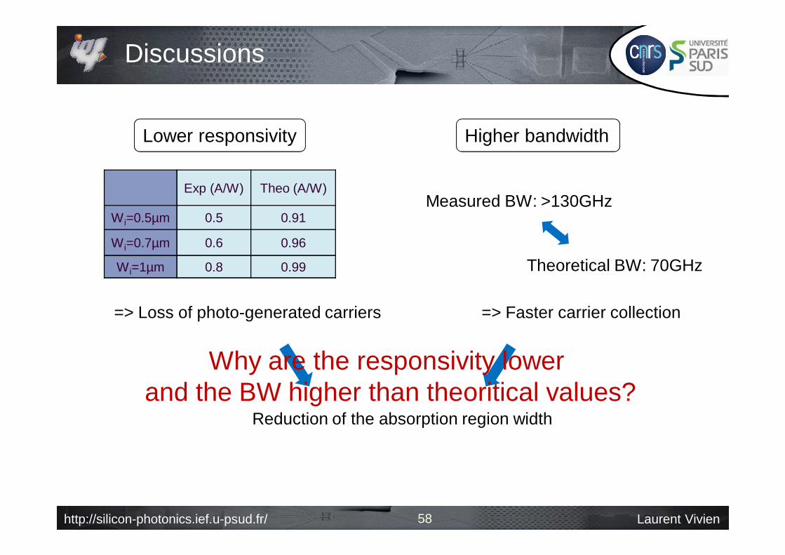
Discussions
58
Lower responsivity Higher bandwidth
=> Loss of photo-generated carriers => Faster carrier collection
Reduction of the absorption region width
Exp (A/W) Theo (A/W)
Wi=0.5µm 0.5 0.91
Wi=0.7µm 0.6 0.96
Wi=1µm 0.8 0.99
Measured BW: >130GHz
Theoretical BW: 70GHz
Why are the responsivity lower and the BW higher than theoritical values?
http://silicon-photonics.ief.u-psud.fr/ Laurent Vivien
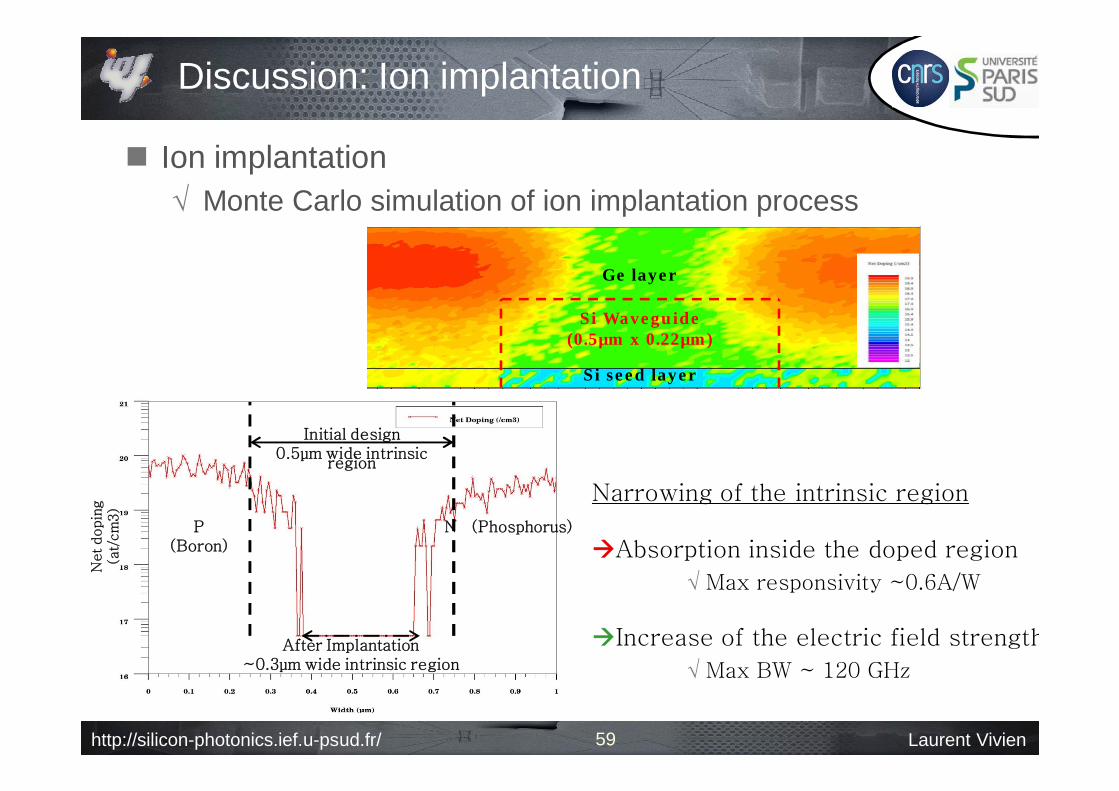
Discussion: Ion implantation
Ion implantation Monte Carlo simulation of ion implantation process
Narrowing of the intrinsic region
Absorption inside the doped region
Max responsivity ~0.6A/W
Increase of the electric field strength
Max BW ~ 120 GHz
Initial design0.5µm wide intrinsic
region
After Implantation~0.3µm wide intrinsic region
P (Boron)
N (Phosphorus)
Net dopin
g
(at/
cm
3)
Ge laye r
Si se e d laye r
Si Wave gu ide(0.5µm x 0.22µm )
59

http://silicon-photonics.ief.u-psud.fr/ Laurent Vivien
Data transmission
10 Gbit/s
20 Gbit/s
30 Gbit/s
40 Gbit/s
Coll.:
Under zero-bias
60
40 Gbit/s @ -1V
Results beyond specifications
High responsivity: > 0.5A/W
High bandwidth: 40Gbit/s
Low dark current: <1nA @ ‐1V
Bias voltage: 0V

http://silicon-photonics.ief.u-psud.fr/ Laurent Vivien61
How can we increase the receiver bandwidth?
….Towards Tbit/s….

http://silicon-photonics.ief.u-psud.fr/ Laurent Vivien
To improve bandwidth of receiver
40Gbit/s detector
Bandwidth = Parallelism x Frequency
Need more wavelengths
1.E-07
1.E-06
1.E-05
1.E-04
1.E-03
1520 1525 1530 1535 1540 1545 1550 1555
Lambda (nm)
Cur
rent
(A)
2 x 16 channels 200GHz centered at about 1550nm … 640 Gbit/s and more…
62

http://silicon-photonics.ief.u-psud.fr/ Laurent Vivien
Conclusion
Germanium photodetectors are more and more considered as a mature silicon photonics devices.
The PD characteristics are close to the one of III-V PD. Incredible at the beginning.
The trends Development of complex circuits for Tbit/s operation Integration with CMOS circuits (TIA) Avalanche PD … new route to reduce the power consumption of the emitterPhoton counting – Quantum optics
63