
Silicon Carbide Bipolar Integrated Circuits for High ... · SiC bipolar junction transistors (BJTs)...
71
Silicon Carbide Bipolar Integrated Circuits for High Temperature Applications LUIGIA LANNI Licentiate Thesis School of Information and Communication Technology (ICT) KTH, Royal Institute of Technology Stockholm, Sweden 2012
Transcript of Silicon Carbide Bipolar Integrated Circuits for High ... · SiC bipolar junction transistors (BJTs)...

Silicon Carbide Bipolar Integrated Circuits
for High Temperature Applications
LUIGIA LANNI
Licentiate Thesis
School of Information and Communication Technology (ICT)KTH, Royal Institute of Technology
Stockholm, Sweden 2012

TRITA-ICT/MAP AVH Report 2012:04ISSN 1653-7610ISRN KTH/ICT-MAP/AVH-2012:04-SEISBN 978-91-7501-244-5
KTH School of Information andCommunication Technology
SE-100 44 StockholmSWEDEN
© Luigia Lanni, Feb 2012

iii
Abstract
Silicon carbide (SiC) is a semiconductor that provides significantadvantages for high-power and high-temperature applications thanksto its wide bandgap, which is several times larger than silicon. Theresulting high breakdown field, high thermal conductivity and highintrinsic temperature (well above 600 °C) allow high temperature op-eration of SiC devices and relaxed cooling requirements. In particular,SiC bipolar junction transistors (BJTs) are suitable for high tempera-ture integrated circuits (ICs), due to the absence of a gate oxide.This work focuses on design, fabrication and characterization of thefirst 4H-SiC integrated circuits realized at KTH. It deals with basicbipolar ICs suitable for high temperature and low voltage applications.Operation up to 300 °C of low-voltage 4H-SiC NPN bipolar transistorsand digital integrated circuits based on emitter coupled logic (ECL)has been demonstrated. In the temperature range 27 - 300 °C stablenoise margins of about 1 V have been achieved for a 2-input OR-NORgate operated on -15 V supply voltage, and an oscillation frequency ofabout 2 MHz has been observed for a 3-stage ring oscillator.The possibility of realizing PNP transistors and passive devices in thesame process technology has also been investigated.

Contents
Abstract iii
Contents iv
List of appended papers vii
Acknowledgements ix
List of symbols and acronyms xi
1 Introduction 1
1.1 The role of high temperature electronics . . . . . . . . . . . . 11.2 SiC: a material for high temperature applications . . . . . . . 3
1.2.1 Crystal structure and polytypism . . . . . . . . . . . . 31.2.2 Electrical properties . . . . . . . . . . . . . . . . . . . 4
1.3 High temperature Integrated Circuits in SiC . . . . . . . . . . 71.4 KTH in-house process for 4H-SiC ICs . . . . . . . . . . . . . 7
2 Modeling, simulation and design 11
2.1 SPICE model for SiC BJTs . . . . . . . . . . . . . . . . . . . 112.2 Physical 2-D device simulation: low voltage NPN . . . . . . . 142.3 Circuit design and simulation . . . . . . . . . . . . . . . . . . 17
2.3.1 OR-NOR gate . . . . . . . . . . . . . . . . . . . . . . 182.3.2 3-stage ring oscillator . . . . . . . . . . . . . . . . . . 20
2.4 IC layout . . . . . . . . . . . . . . . . . . . . . . . . . . . . . 212.4.1 Transistors: NPN and PNP . . . . . . . . . . . . . . . 232.4.2 Integrated resistors . . . . . . . . . . . . . . . . . . . . 242.4.3 Circuits . . . . . . . . . . . . . . . . . . . . . . . . . . 25
iv

CONTENTS v
3 Fabrication 27
3.1 Wafer cleaning . . . . . . . . . . . . . . . . . . . . . . . . . . 293.2 Lithography . . . . . . . . . . . . . . . . . . . . . . . . . . . . 303.3 SiC etching . . . . . . . . . . . . . . . . . . . . . . . . . . . . 303.4 Oxidation and oxide deposition . . . . . . . . . . . . . . . . . 313.5 Metallization . . . . . . . . . . . . . . . . . . . . . . . . . . . 31
4 Measurement results and performance evaluation 35
4.1 Active and passive device performance . . . . . . . . . . . . . 354.1.1 PNP transistor . . . . . . . . . . . . . . . . . . . . . . 354.1.2 Integrated resistors . . . . . . . . . . . . . . . . . . . . 384.1.3 Low voltage NPN transistor . . . . . . . . . . . . . . . 41
4.2 Circuit performance . . . . . . . . . . . . . . . . . . . . . . . 444.2.1 OR-NOR gate . . . . . . . . . . . . . . . . . . . . . . 444.2.2 Ring oscillator . . . . . . . . . . . . . . . . . . . . . . 48
5 Conclusions and future work 51
Bibliography 55


List of appended papers
I “Measurements and simulations of lateral PNP transistors in
a SiC NPN BJT technology for high temperature integrated
circuits”
L. Lanni, R. Ghandi, M. Domeij, C.-M. Zetterling, B. G. Malm, M.Östling, Materials Science Forum, v 679-680, p 758-761, 2011. Proceed-ings of European Conference on Silicon Carbibe and Related Materials2010.
II “Bipolar Integrated OR-NOR Gate in 4H-SiC”
L. Lanni, R. Ghandi, B. G. Malm, C.-M. Zetterling, M. Östling, To bepublished in Materials Science Forum 2012. Proceedings of Interna-tional Conference on Silicon Carbibe and Related Materials 2011.
III “Design and Characterization of High Temperature ECL-based
Bipolar Integrated Circuits in 4H-SiC”
L. Lanni, R. Ghandi, B. G. Malm, C.-M. Zetterling, M. Östling, ac-cepted for publication in IEEE Transaction on Electron Devices 2012.
It is worth noticing that results discussed in PAPER II and III partiallyoverlap. PAPER II aims to report a 4H-SiC process technology suitable forhigh temperature ICs showing the high temperature operation of differentdevices and OR-NOR gates while PAPER III focuses on the performanceachieved by an OR-NOR gate and a ring oscillator fabricated in the samebatch.
Author’s contribution to each paper:
I 100% of electrical characterization, 100% of simulations, 90% of writingthe manuscript.
vii

viii List of appended papers
II 90% of processing, 100% of electrical characterization, 100% of simula-tions, 90% of writing the manuscript.
III 90% of processing, 100% of electrical characterization, 100% of simula-tions, 90% of writing the manuscript.

Acknowledgements
My deep gratitude goes to Prof. Carl-Mikael Zetterling for having initiatedme into the fascinating world of research, at beginning supervising me dur-ing my master thesis and then giving me the opportunity to continue mystudy starting my Ph.D. in the field of SiC integrated circuits. I am verygrateful to him for his guidance and motivation in these first two years.Although he is very busy, especially recently with all the new students, healways finds time for discussing all kind of issues related to my project andto read and correct my papers, as well as this thesis.
Prof. Gunnar Malm, my second supervisor is deeply appreciated for in-sightful discussions, the valuable assistance with the measurements and hiscontinous support, especially in critical moments.
Prof. Mikael Östling, my third supervisor and head of the device technologydepartment, is thanked for having accepted me as Ph.D. student and for hissupport and guidance in the research world.
I am also indebted to Dr. Reza Ghandi, my first officemate, for having in-troduced me to the clean room work and SiC process technology. I am verygrateful for his support, encouragement and all the valuable advices for bothacademic and daily life. His assistance during the last days of my first batchand the long discussions at the office before leaving and via email recentlyare sincerely appreciated.Jan-Olov Svedberg and Krister Gumaelius at Fairchild Semiconductor (onceTranSiC) are also thanked for their assistance and insightful advices in prob-lematic processing issues.
Dr. Martin Domeij, Docent Henry Radamson, Prof. Anders Hallen, DocentPer-Erik Hellström and Prof. Ana Rusu are deeply appreciated for theirkind scientific support and assistance.
The other people at SiC group have kindly helped and supported me, which
ix

x Acknowledgements
have been and is essential for my research activity. Special thanks go toBenedetto Buono for fruitful discussions about semiconductor physics andsimulation techniques. Above all I am grateful to him for the great patienceand the continuous support in these two years, especially after stressful daysin clean room and at the last ICSCRM.I am also thankful to Romain Esteve for having been a good friend and forfruitful discussions and assistance in clean room.I would like to express also my gratitude to Katarina Smedfors for the en-joyble and interesting time we spent together in clean room, although manythings went wrong. I hope we will work more together.Arash Salemi (my officemate) and Muhammad Usman are appreciated forvery nice discussions. Dr. Ming Hung Weng is thanked for the time spenttogether at the beginning of my clean room experience.
Eugenio Dentoni Litta is thanked for his continuous encouragement andsupport not only during the long days in clean room. Also Dr. Mo-hammadreza Kolahdouz (Mreza), Timo Söderqvist, Christian Ridder, Dr.Yong-Bin Wang, Dr. Margareta Linarsson, Dr. Jun Luo, Dr. JiantongLi, Dr. Valur Gudmundsson, Sam Vaziri, Oscar Gustafsson, Maziar AmirManouchehry Naiini and Dr. Christof Henkel at EKT and my other friends,Sergey Manuilov, Ana Lopez, Reza Sanatinia are thanked and appreciatedfor the encouragement during these first two years.
I would like also to thank vary kind people at the Electrum Lab for helpand nonstop assistance. Foremost I would like to thank Reza Nikpars andArman Sikiric, for their help with the lab machines and also for their kindand friendly attitude.A special thanks to Gunilla Gabrielsson for her warm kindness and help inall bureaucratic issues.
Last but not least I would like to express my sincere gratitude to my familyfor the continuous support and encouragement, and to my friends of always:Giorgia Longobardi, Giovanna Lanni and Stella Lanni. I am deeply grate-ful to Giorgia for the long (very long) conversations on skype late in theevening, for her great understanding and valuable advices.
Thank you all!
Luigia Lanni,January 2012

List of symbols and acronyms
β Current gain
βF Forward current gain
βR Reverse current gain
ǫ Permittivity
µn Electron mobility
µp Hole mobility
A Ampere
Al Aluminum
Ar Argon
BHF Buffered hydrogen fluoride
BJT Bipolar junction transistor
C Carbon
CH3CH(OH)CH3 Isopropanol
Cl2 Chlorine gas
CMOS Complementary metal-oxide semiconductor
CVD Chemical Vapor Deposition
EC Critical electric field
ECL Emitter coupled logic
xi

xii List of symbols and acronyms
EG Energy bandgap
FGP Forward Gummel Poon
fosc Oscillation frequency
HBr Hydrogen bromide
HCl Hydrochloric acid
HF Hydrogen fluoride
HNO3 Nitric acid
HV High voltage
H2O Water
H2O2 Hydrogen peroxide
H2SO4 Sulfuric acid
IC Integrated circuit
ICP Inductively coupled plasma
IB Base current
IC Collector current
IE Emitter current
JFET Junction field effect transistor
k Boltzmann constant
n Electron concentration
NC Density of states in conduction band
ND Net doping concentration for n-type doping
NH4F Ammonium fluoride
NH4OH Ammonium hydroxide
ni Intrinsic carrier concentration
Ni Nickel

List of symbols and acronyms xiii
NM Noise margin
NMH High level NM
NML Low level NM
NO Nitric oxide
NPN Bipolar junction transistor where emitter, base and collectorare n-, p- and n-doped respectively
NV Density of states in valence band
N2O Nitrous oxide
p Hole concentration
PECVD Plasma Enhanced Chemical Vapor Deposition
PNP Bipolar junction transistor where emitter, base and collectorare p-, n- and p-doped respectively
q Elementary charge
RGP Reverse Gummel Poon
RIE Reactive ion etching
Ron−sp Specific on resistance
s Second
SEM scanning electron microscopy
Si Silicon
SiC Silicon carbide
SiO2 Silicon dioxide
T Temperature
tf Fall time
Ti Titanium
TLM Transfer length method
Tosc Oscillation period

xiv List of symbols and acronyms
TP Propagation delay
TP HL High-to-low propagation delay
TP LH Low-to-high propagation delay
tr Rise time
TTL Transistor-transistor logic
V Voltage
VBR Breakdown voltage
VBC Base-collector voltage
VCE Collector-emitter voltage
VEC Emitter-collector voltage
VEE Voltage supply
VIN Input voltage
VNOR NOR output voltage
VOR OR output voltage
VOUT Output voltage
VTC Voltage transfer characteristic
W Drift region thickness
WE Emitter width
Wp Distance between emitter layer edge and base contact edge

Chapter 1
Introduction
Although silicon carbide (SiC) is very well-known for its high blocking ca-pability and much research has been performed in this field, this work dealswith low voltage 4H-SiC integrated circuits capable of high temperature op-eration, especially approaching 300 °C and beyond. The goal of this work isto develop an enviroment that will allow to design and fabricate high per-formance bipolar integrated circuits (ICs) in 4H-SiC. Several aspects con-cerning their realization are involved: modeling, design, fabrication andcharacterization of devices and circuits.This thesis is organized in four main chapters. The first starts discussing theneed for high temperature electronics, then it briefly describes SiC electri-cal properties, with particular attention on advantages for high temperatureapplications; it continues with an overview of high temperature ICs in SiCand finally it illustrates device and circuit technology selected for this work.The second and third focus on theoretical and experimental studies per-formed in order to fabricate ICs in 4H-SiC. The fourth reports simulationand measurement results for both isolated devices and integrated circuits.The thesis ends by summarizing the results achieved up to now and plan-ning future studies intended to develop the discussed technology, as well asto improve the device and circuit performance.
1.1 The role of high temperature electronics
High temperature operation of semiconductor-based devices is required inmany important applications, such as transportation or energy sector indus-
1
2 CHAPTER 1. INTRODUCTION
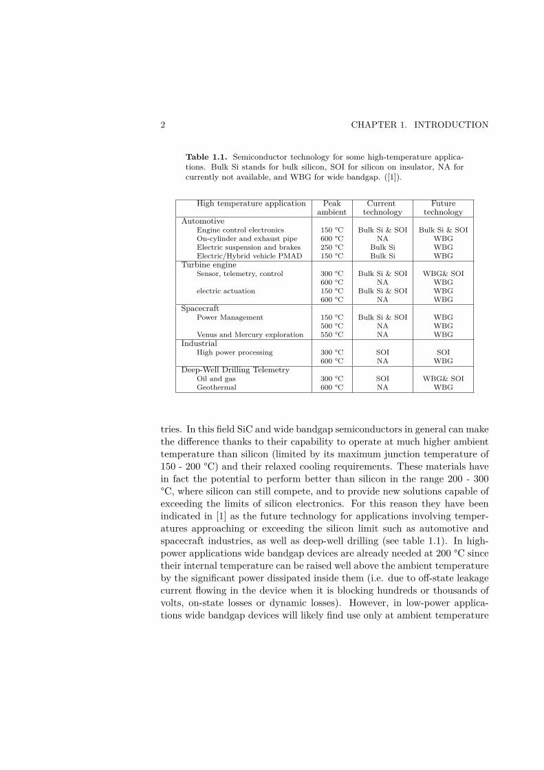
Table 1.1. Semiconductor technology for some high-temperature applica-tions. Bulk Si stands for bulk silicon, SOI for silicon on insulator, NA forcurrently not available, and WBG for wide bandgap. ([1]).
High temperature application Peak Current Futureambient technology technology
AutomotiveEngine control electronics 150 °C Bulk Si & SOI Bulk Si & SOIOn-cylinder and exhaust pipe 600 °C NA WBGElectric suspension and brakes 250 °C Bulk Si WBGElectric/Hybrid vehicle PMAD 150 °C Bulk Si WBG
Turbine engineSensor, telemetry, control 300 °C Bulk Si & SOI WBG& SOI
600 °C NA WBGelectric actuation 150 °C Bulk Si & SOI WBG
600 °C NA WBGSpacecraft
Power Management 150 °C Bulk Si & SOI WBG500 °C NA WBG
Venus and Mercury exploration 550 °C NA WBGIndustrial
High power processing 300 °C SOI SOI600 °C NA WBG
Deep-Well Drilling TelemetryOil and gas 300 °C SOI WBG& SOIGeothermal 600 °C NA WBG
tries. In this field SiC and wide bandgap semiconductors in general can makethe difference thanks to their capability to operate at much higher ambienttemperature than silicon (limited by its maximum junction temperature of150 - 200 °C) and their relaxed cooling requirements. These materials havein fact the potential to perform better than silicon in the range 200 - 300°C, where silicon can still compete, and to provide new solutions capable ofexceeding the limits of silicon electronics. For this reason they have beenindicated in [1] as the future technology for applications involving temper-atures approaching or exceeding the silicon limit such as automotive andspacecraft industries, as well as deep-well drilling (see table 1.1). In high-power applications wide bandgap devices are already needed at 200 °C sincetheir internal temperature can be raised well above the ambient temperatureby the significant power dissipated inside them (i.e. due to off-state leakagecurrent flowing in the device when it is blocking hundreds or thousands ofvolts, on-state losses or dynamic losses). However, in low-power applica-tions wide bandgap devices will likely find use only at ambient temperature

1.2. SIC: A MATERIAL FOR HIGH TEMPERATURE APPLICATIONS 3
(a)
(b)
Figure 1.1. (a) - Tetrahedron building block of all SiC crystals. (b) -Crystal structure of different SiC polytypes: 2H, 3C, 4H, 6H. Top view.([2]). ([3]).
above 300 °C, since silicon and silicon-on-insulator technologies are alreadyproviding very large scale integrated circuits in this temperature range [1].
1.2 SiC: a material for high temperature applications
SiC, due to its crystal structure, provides significant advantages for appli-cations requiring high temperature operation and/or high power. It is infact characterized by a thermal conductivity (about 5 W/cm · K) two orthree times larger than silicon, an intrinsic concentration orders of magni-tude lower than silicon at room temperature and a critical field (2 MV/cm)10 times larger than silicon.
1.2.1 Crystal structure and polytypism
SiC crystal structure is composed by Si and C atoms organized in a basicblock consisting of a tetrahedron of four carbon atoms covalently bondedwith a silicon atom in the center, as depicted in Fig. 1.1 (a). The approxi-

4 CHAPTER 1. INTRODUCTION
mate bond length between a carbon and a silicon atom is 1.89 Å while thedistance between the Si-Si or C-C atoms is 3.08 Å. According to the way inwhich the basic units are connected together different crystal structures canbe formed. Each crystal structure is named polytype and the characteris-tic to form different polytypes is called polytypism. All polytypes have anhexagonal frame of SiC bilayers, which can be described as sheets of sphereswith constant radius and distance between each others as illustrated in Fig.1.1 (b). Even if the sheets are the same for all lattice planes, the way inwhich they are stacked can differ: each plane, consisting of a double layersof carbon and silicon atoms, is shifted according to the adjacent planes inorder to fit in their "valleys". This gives rise to three different positions ofthe planes, and so to different polytypes according to the specific repetitiveorder in which the sheets are arranged as depicted in Fig. 1.1 (b). The nameof each polytype is characterized by a number and a letter: the number in-dicates how many layers form the basic sequence, and the letter determinesthe resulting structure of the crystal: C for cubic, H for hexagonal, and Rfor rhombohedral.
1.2.2 Electrical properties
Some of the most important electric properties of SiC are summarized intable 1.2 for different polytypes. Although they have the same proportionof silicon and carbon atoms, electronic and optical properties as well asthe unit cell and the number of atoms per unit cell differ between differentpolytypes as consequence of the different stacking sequence between theplanes.
Wide bandgap
At room temperature the energy bandgap of SiC ranges from 2.2 eV to 3.2eV depending on the polytype. It is 2-3 times larger than silicon (1.12 eV).The intrinsic concentration (ni) is therefore orders of magnitude lower thanin silicon. This is maybe the main reason for the interest in wide bandgapsemiconductors for high temperature applications [1]. Semiconductor deviceoperation is in fact based on the control of free carrier concentration, whichis achieved during the fabrication through introduction of desired amount ofdopants in selected regions of the device. However, a certain amount of freecarriers is already present in the semiconductor crystal itself (the intrinsic

1.2. SIC: A MATERIAL FOR HIGH TEMPERATURE APPLICATIONS 5
Table 1.2. Electrical properties of Si and SiC. (1) indicates perpendicularto c-axis, (2) parallel to c-axis. ([2]).
Property Si 3C-SiC 6H-SiC 4H-SiC
Bandgap,Eg 1.12 2.4 3.0 3.2
[eV] at room temperature
Critical field, EC 0.25 2.0 2.5 2.2
[MV/cm]
Thermal Conductivity λ 1.5 5 5 5
[W/cmK] at room temperature
Saturated electron drift velocity, vsat 1.0 2.5 2.0 2.0
[107 cm/s]
Electron mobility, µn 1350 1000 900(1) 950(1)
[cm2/Vs] 100(2) 1150(2)
Hole mobility, µp 480 40 80 120
[cm2/Vs]
Relative dielectric constant, ǫr 11.9 9.7 10 10
[adim]
concentration), and it depends on temperature as follows [5]:
ni =√
NC NV e−EG/2kT , (1.1)
where NC and NV are the effective electron and hole densities of states(cm−3), EG is the bandgap in electronvolts, k the Boltzmann constant(8.62 × 10⁻⁵eV/K) and T the temperature in Kelvin. Although EG, NC andNV are also temperature dependent, equation (1.1) is governed by the expo-nential term. When the temperature is high enough to make ni comparablewith the inserted doping concentration, the device behavior is undesirableaffected by the intrinsic concentration. In SiC this can occur at temperaturebeyond 1000 °C, where ni approaches 1015 cm−3 (usually considered a lowdoping concentration), while for Si it takes place about 200 - 300 °C. Thisis shown in Fig. 1.2, which depicts the intrinsic concentration in silicon anddifferent SiC polytypes as function of the temperature.
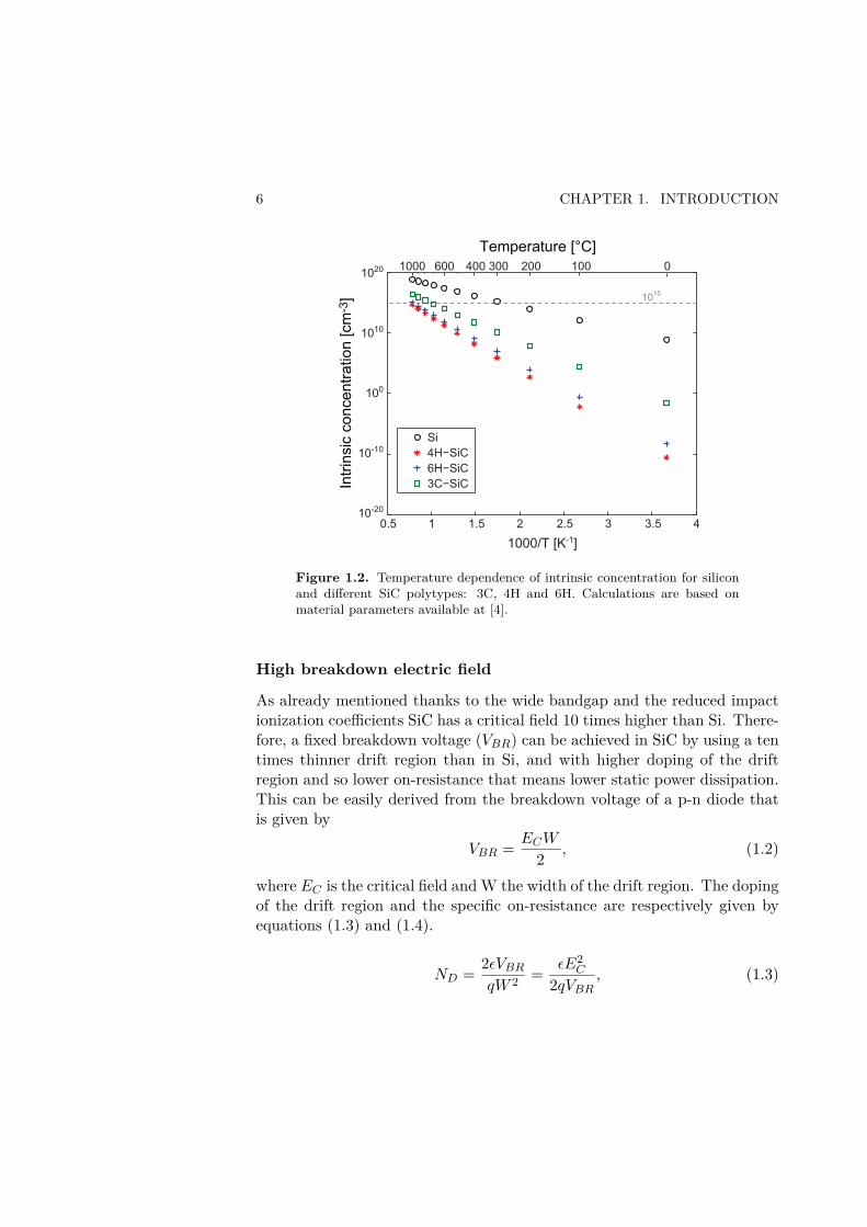
6 CHAPTER 1. INTRODUCTION
1000 600 400 300 200 100
0.5 1 1.5 2 2.5 3 3.5 4
Si
4H−SiC
6H−SiC
3C−SiC
1010
1020
1000/T [K-1]
Temperature [°C]
Intr
insic
co
nce
ntr
atio
n [cm
-3]
100
10-20
10-10
0
1015
Figure 1.2. Temperature dependence of intrinsic concentration for siliconand different SiC polytypes: 3C, 4H and 6H. Calculations are based onmaterial parameters available at [4].
High breakdown electric field
As already mentioned thanks to the wide bandgap and the reduced impactionization coefficients SiC has a critical field 10 times higher than Si. There-fore, a fixed breakdown voltage (VBR) can be achieved in SiC by using a tentimes thinner drift region than in Si, and with higher doping of the driftregion and so lower on-resistance that means lower static power dissipation.This can be easily derived from the breakdown voltage of a p-n diode thatis given by
VBR =ECW
2, (1.2)
where EC is the critical field and W the width of the drift region. The dopingof the drift region and the specific on-resistance are respectively given byequations (1.3) and (1.4).
ND =2ǫVBR
qW 2=
ǫE2C
2qVBR, (1.3)

1.3. HIGH TEMPERATURE INTEGRATED CIRCUITS IN SIC 7
Ron−sp =W
qµnND=
4V 2BR
ǫµnE3C
. (1.4)
High thermal conductivity
SiC high thermal conductivity results in a bigger capability of SiC devices totransport heat out of themselves. This is very useful in high-power and high-frequency electronics where large amounts of heat are generated and need tobe transported away in order to prevent devices not only from degradationof their performance but also from failure.
1.3 High temperature Integrated Circuits in SiC
High temperature operation of ICs has already been reported in SiC. Long-term stability of JFET ICs, both analogue and digital, has been demon-strated in 6H-SiC with circuit operation at 500 °C for thousand hours [6].CMOS technology has been investigated in the early 90s in 6H-SiC [7] andrecently reported in 4H-SiC [8]. In both of the cases, 300 °C operation ofdigital circuits has been shown. Bipolar ICs have also been demonstratedin 4H-SiC with operation up to 355 °C of transistor-transistor logic (TTL)[9] and propagation delays comparable with those of Silicon TTL circuits(≈10ns) [10]-[11].This work proposes a bipolar technology in 4H-SiC and integrated circuitsbased on emitter coupled logic (ECL). The ECL permits a wide operatingrange both in terms of temperature and supply voltage since it is based ondifferential stages and allows an easy implementation of a temperature andsupply voltage compensation network. Furthermore, being a non-saturatedlogic the ECL has the potential to achieve high operation speed.
1.4 KTH in-house process for 4H-SiC ICs
The realization of ICs in SiC involves not only circuit design and simulationbut also design and modeling of required active and passive devices, as wellas the availability of a process technology suitable for ICs. Device andcircuit level simulations of bipolar transistors are also necessary in order todesign the epitaxial structure to be processed and to extract all the SPICEmodels necessary for circuit simulation. All the steps performed to realize

8 CHAPTER 1. INTRODUCTION
High voltage batch:
MEASUREMENTS on 1-F BJT at T1, T2, ...Tm
(FGP, IC-VCE, RGP, IE-VEC)
BJT SPICE model
extraction at T1, T2, ...Tm
COMPARISON:
measured and simulated
CIRCUIT characteristics
batch i (i>0)
Is the
simulated circuit
available in a previous
BATCH?
Final
CIRCUIT DESIGN
batch i+1, i = 0, ... n
MATLAB SPICE
.cir (netlist)
.out (sim. results)
CIRCUIT
DESIGN
YES NO
2-D DEVICE SIMULATIONS
of low voltage BJT, batch i+1, i = 0, ... n
(FGP, IC-VCE)
Epitaxial structure and
BJT geometry DESIGN
batch i+1, i = 0, ... n SPICE models at T1, T2, ...Tm
for BJT from batch i, i = 0, ... n
LAYOUT
Resistors,
test structuresBJTs Circuits
Mask set i+1, i = 0, ...n
from external supplier
epitaxial growth
from external supplier
FABRICATION
batch i+1, i = 0, ...n
MEASUREMENTS batch i+1, i = 0, ... n
BJTs CircuitsTest structures
COMPARISON:
measured and
simulated DEVICE
characteristics
CIRCUIT SIMULATIONS
at T1, T2, ...Tm batch i+1, i = 0, ... n
and batch i if i > 0
Figure 1.3. Flowchart describing the different steps performed to realizethe first batch of ICs in SiC and those that will lead to successive batches.The feedback between previous and successive IC batches is highlighted byred arrows (dotted lines), whereas green arrows (dashed lines) indicate stepsused only for the first batch.

1.4. KTH IN-HOUSE PROCESS FOR 4H-SIC ICS 9
the first IC batch, presented in this thesis, as well as those that will resultin a second IC batch are schematically described in Fig. 1.3. This work hasbeen initiated by using a high voltage bipolar process technology developedat KTH [12] [13]. Characterization of single finger BJTs realized in a highvoltage batch [12] has been used to extract SPICE models for SiC BJTsand a process technology suitable for ICs has been derived from the highvoltage one. Characterization of active and passive devices fabricated inthe first IC batch provides feedback on the fabrication process and betterSPICE models, which together with circuit measurement results will allowto design more advanced circuits and to improve the performance of thecircuits investigated in the first batch by acting on circuit diagram and/orlayout.


Chapter 2
Modeling, simulation and design
This chapter describes the modeling, simulation and design, at both deviceand circuit level, necessary for the fabrication of SiC ICs, as briefly discussedin the previous chapter (section 1.4). It starts with SPICE model extractionfor SiC bipolar transistors, which has been performed for high voltage singlefinger BJTs, and device level simulation. The goal is to design a bipolartransistor (its epitaxial structure and geometry) for high temperature ICsthat shows performance similar to that of the high voltage single finger BJTswhen operated in the low voltage range. The chapter continues describingsome of the circuits designed for the first batch.
2.1 SPICE model for SiC BJTs
Among the different parameters included in the Gummel Poon model, onlyfew of them have been used to describe the behavior of SiC BJTs. Onlystatic parameters, for both forward and reverse bias, and those related tospace charge capacitances have been taken into account. The reason forthis choice is to have a simple SPICE model approprate for static circuitsimulation. The first goal of this study is in fact to demonstrate the hightemperature operation of ECL ICs in 4H-SiC. The complete list of the con-sidered parameters is given in table 2.1. Two different temperatures havebeen considered: 27 and 200 C. For each one a different SPICE modelparameter set has been extracted. At this stage no temperature dependence
11

12 CHAPTER 2. MODELING, SIMULATION AND DESIGN
Table 2.1. High voltage single finger BJT. Extracted SPICE model param-eters based on a graphical extraction and an optimization routine able to fitmeasured and simulated characteristics.
Parameter Description 27 C 200 C Unit
IS Transport Saturation 9.3 10−46 3.8 10−35 A
Current
NF Forward Current Emission 1.10 1.24 adim
Coefficient
NR Reverse Current Emission 1.09 1.22 adim
Coefficient
BF Ideal Maximum Forward Beta 62 32 adim
BR Ideal Maximum Reverse Beta 0.31 0.28 adim
NE Base Emitter Leakage 2.83 3.52 adim
Emission Coefficient
IKF Knee Current for Forward Beta 0.358 0.002 A
High Current Roll-off
IKR Knee Current for Reverse Beta 0.068 0.011 A
High Current Roll-off
ISE Base Emitter Leakage 2.7 10−21 6.3 10−16 A
Saturation Current
ISC Base Collector Leakage 3.8 10−19 8.9 10−16 A
Saturation Current
RC Collector Resistance 18 18 Ω
RB Base Resistance 41 8 Ω
RE Emitter Resistance 18 25 Ω
VAF Forward Early Voltage 400 645 V
VAR Reverse Early Voltage 38 45 V
RCO Epitaxial region resistance 12 85 Ω
GAMMA Epitaxial region doping factor 1.2 10−43 2.4 10−35 adim
VJC Base Collector Built-in Potential 2.85 2.18 V
CJC Base Collector Zero Bias 4.52 10−12 5.09 10−12 F
Capacitance
MJC Base Collector Junction 0.5 0.5 adim
Grading Coefficient
VJE Base Emitter Built-in Potential 2.95 2.72 V
CJE Base Emitter Zero Bias 28.16 10−12 29.41 10−12 F
Capacitance
MJE Base Emitter Junction 0.5 0.5 adim
Grading Coefficient

2.1. SPICE MODEL FOR SIC BJTS 13
MEASUREMENT of BJT characteristics at T*
(FGP, IC-VCE, RGP, IE-VEC)
Graphical extraction of
selected SPICE model parameters
model parameter set at T*
after optimization step i, i = 0, ..., n
Do
all couples
of measurements
and simulations
match?
Final SPICE model
parameter set at T*
ADJUSTMENT of the latest
parameter set (optimization step i)
in order to match selected
measured BJT characteristicsMATLAB SPICE
.cir (netlist)
.out (simulation results)
SPICE SIMULATION of selected
BJT characteristics at T*
(FGP, IC-VCE, RGP, IE-VEC)
i + 1
i = 0
YES
NO
Figure 2.1. Flowchart describing the procedure used for extracting BJTSPICE model parameters.
has been modeled1. For each temperature a set of four measured character-istics has been considered: forward and reverse Gummel plots and outputcharacteristics. First each parameter has been derived independently from
1All SPICE simulations in this work have been performed by setting the temperatureat its default value (27 C) and by using the BJT SPICE model extracted at the desiredtemperature. In this way the simulator does not apply any correction to the given devicemodel; which it automatically does when the temperature is different from 27 C.
14 CHAPTER 2. MODELING, SIMULATION AND DESIGN
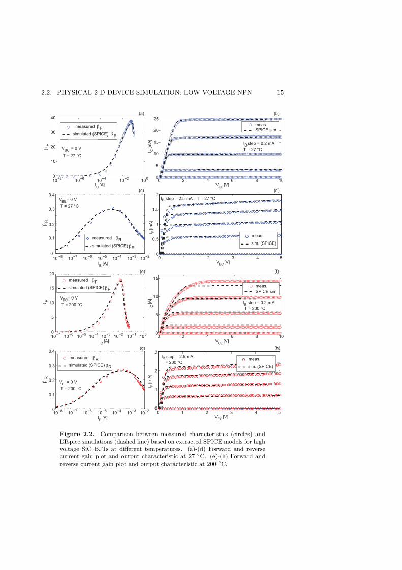
the others by the means of a graphical extraction procedure that takes intoaccount the parameter physical meanings [14] [15]. Then, an optimizationroutine has been performed by using as starting point the parameter valuesobtained with the graphical extraction in order to achieve a set of parametersthat accounts for interaction between different parameters. The optimiza-tion routine consists of successive adjustments of the parameter values untila satisfactory agreement is reached between all four measured characteris-tics and those predicted by LTspice [16] simulations at the same time. Theblock diagram of this procedure is given in Fig. 2.1. SPICE simulations,as well as comparison between simulation and measurement results, havebeen performed by interfacing MATLAB with a SPICE simulator [17] [18].A MATLAB code has been used to write the netlist that loads the latestBJT SPICE model and reproduces performed measurement, to run it bycalling LTspice and to read the simulation results. Extracted parameters at27 and 200 C are given in table 2.1 for single finger BJTs fabricated in ahigh voltage batch [12], while a comparison between simulated and measuredcharacteristics, both forward and reverse, is shown in Fig. 2.2. A quite goodagreement has been achieved for all the characteristics except for the out-put characteristic at 200 C, where the observed quasi saturation, typicalfor high voltage bipolar transistors, is not well modeled. A further effortin the optimization process has not been performed since this phenomenonwas not expected to happen in the low voltage BJT.
2.2 Physical 2-D device simulation: low voltage NPN
2-D simulations have been performed by using Sentaurus TCAD [19] in or-der to design an appropriate epitaxial structure for the low voltage bipolartransistors2. The attention has been focused on forward current gain depen-dence on temperature in the range 27 - 200 C. The epitaxial structure usedin the high voltage batch [12] and the one that was selected for this work areshown in Fig.s 2.3 (a) and (b) respectively. Compared to the high-voltagesturcture, the low-voltage one uses two extra layers: a high doped collectorlayer and a further p-layer as first epi-layer. The first one provides a goodohmic contact to the collector region making it accessible on the top sur-face, whereas the second one allows to isolate different devices in the same
2The intention was to design a BJT whose behavior in the low voltage range could bepredicted by the SPICE models obtained in the previous section.
2.2. PHYSICAL 2-D DEVICE SIMULATION: LOW VOLTAGE NPN 15
0 2 4 6 8 100
5
10
15
20
25
VCE
[V]
I C [m
A]
meas.
SPICE sim.
IB step = 0.2 mA
T = 27 °C
10−8
10−6
10−4
10−2
100
0
10
20
30
40
IC [A]
β F
measured βF
simulated (SPICE) β F
VBC
= 0 V
T = 27 °C
0
0.1
0.2
0.3
0.4
β R
10−7
10−6
10−5
10−4
10−3
10−2
10−8
IE [A]
VBE
= 0 V
T = 27 °C
measured R
simulated (SPICE) R
β
β
0 1 2 3 4 5V
EC [V]
I E [m
A]
0
1
2
0.5
1.5
IB step = 2.5 mA T = 27 °C
meas.
sim. (SPICE)
(a) (b)
(c) (d)
0 2 4 6 8 100
5
10
15
VCE
[V]
I C [A
]
meas.
SPICE sim.
IB step = 0.2 mA
T = 200 °C
10−7
10−6
10−5
10−4
10−3
10−2
10−1
100
0
5
10
15
20
IC [A]
β F
measured F
simulated (SPICE) F
VBC
= 0 V
T = 200 °C
β
β
0
0.1
0.2
0.3
0.4
10−7
10−6
10−5
10−4
10−3
10−2
10−8
IE [A]
β R
VBE
= 0 V
T = 200 °C
measured R
simulated (SPICE) R
β
β
0 1 2 3 4 5V
EC [V]
I E [m
A]
0
1
2
3IB step = 2.5 mA
T = 200 °Cmeas.
sim. (SPICE)
(e) (f)
(g) (h)
Figure 2.2. Comparison between measured characteristics (circles) andLTspice simulations (dashed line) based on extracted SPICE models for highvoltage SiC BJTs at different temperatures. (a)-(d) Forward and reversecurrent gain plot and output characteristic at 27 C. (e)-(h) Forward andreverse current gain plot and output characteristic at 200 C.

16 CHAPTER 2. MODELING, SIMULATION AND DESIGN
Emitter Contact
Base
Contact
Base
Contact
Collector
Contact
n-type substrate
N+ Collector ND = 1 x 1019cm-3
N- Collector ND = 1 x 1016cm-3
P Base NA = 1.4 x 1018cm-3
N+ Emitter
ND = 1 x 1019cm-3
ND = 3 x 1019cm-30.2 µm
0.8 µm
0.3 µm
1 µm
1 µm
2 µm P isolation layer NA = 1.4 x 1018cm-3
30µm35µm 35µm 60µm
(a) (b)High Voltage NPN
Technology
Low Voltage IC
Technology
Emitter Contact
Base
Contact
Collector Contact
N+ substrate
ND = 3 x 1015cm-3
NA ∼ 3.5 x 1017cm-3
ND = 1 x 1019cm-3
ND = 4 x 1019cm-30.2 µm
0.8 µm
0.73 µm
20 µm JTE
Passivation
Layer
12.5µm
Emitter Contact
Base
Contact
Collector Contact
ND
NA
ND
ND
Simulated Structure
WE / 2
Wp
Figure 2.3. Cross sectional views of SiC NPN transistors. (a) - Highvoltage BJT: half structure [12]. (b) - Low voltage NPN transistor designedin this work: entire structure and simulated cross section (left to right).
wafer. Moreover, base and collector layers have been shrunk; the designedcollector thickness is only 1 µm instead of 20 µm required for the HV devicesince no high breakdown voltage is required. The reduced thickness of theepi-layers also helps relaxing the requirements on the step coverage of theinterconnects, which will be discussed in chapter 3.2-D simulations have been performed by using the simplified device cross-section depicted in Fig. 2.3 (b)-right and model parameters available inliterature [20] aiming to obtain similar current gains for the two devices inthe selected temperature range. The measured current gain for a single fin-ger high-voltage BJT decreases with temperature from 40 at 27 C downto 21 at 200 C. In a similar way the simulated current gain for the lowvoltage NPN goes from 39 to 25 in the same temperature range, as shown inFig. 2.4 (a). Further simulations have been performed at 27 C for the lowvoltage BJT in order to investigate its current gain dependence on distancebetween emitter edge and base contact edge (Wp) and half emitter width(WE/2), since these geometrical parameters can significantly affect the tran-sistor current gain [21]. Concerning Wp a too small value can deterioratethe current gain because of an increased recombination in the base. A toonarrow emitter can reduce the device current gain because of the increasedrecombination in the emitter region, whereas if the emitter is too wide thecurrent does not flow through the entire emitter width but it crowds close to

2.3. CIRCUIT DESIGN AND SIMULATION 17
0 50 100 150 20020
25
30
35
40
45
Temperature [°C]
Fo
rwa
rd C
urr
en
t G
ain
measured
(HV single finger BJT)
simulated
(LV NPN for IC)
LV NPN for IC:
WE = 30 µm, Wp = 2.5 µm
2 4 6 8 10 120.94
0.96
0.98
1.00
No
rma
lize
d β
14
WE / 2 [µm]
0 2 4 6 8 10 120.90
0.95
1.00
14Wp [µm]
No
rma
lize
d β
(a) (b)
(c)
LV NPN for IC:
Wp = 2.5 µm
LV NPN for IC:
WE = 30 µm
T=27°C
T=27°C
Figure 2.4. 2-D device simulation results for the low voltage NPN tran-sistor. (a) - Forward current gain vs temperature (circles) compared tomeasured current gain on the high voltage BJT (stars) in the range 27 - 200C. (b) - Normalized βF dependence on half emitter width (WE/2) at 27C. (c) - Normalized βF dependence on distance between base contact andemitter layer edge (Wp) at 27 C. In (b) and (c) red stars indicate simulationresults for selected WE/2 (15 µm) and Wp (2.5 µm).
the base contact due to the depolarization of the base emitter junction. Thisphenomenon causes the saturation of the current gain for further increasingof the emitter width, and so of the overall BJT area. Simulation results areshown in Fig.s 2.4 (b) and (c), where the red markers indicate WE/2 andWp values selected for the low voltage NPN, 15 µm and 2.5 µm respectively.Even if in these simulations only a rough estimation of the effect of WE/2and Wp on BJT current gain has been performed, it is of interest in theprospective of shrinking the overall device area in future batches.
2.3 Circuit design and simulation
Thanks to the extraction of appropriate SPICE models for SiC BJT, it hasbeen possible to design some circuits by the means of LTspice [16] simula-tions. They have been run by using a MATLAB interface that allows towrite the netlist, execute it in LTspice and read the simulation results.

18 CHAPTER 2. MODELING, SIMULATION AND DESIGN
Vref
GND
A
Vout (NOR)
Vout (OR)
VEE= -15V
Q7
R1aQ5RC2
Q10
Q8
R1b
Ree
Q6
Ri2
Q1
Rout1
Reb
Ri1Q4
Q2
Rout2
Q3
R2
RC1
Q9
Differential
input stage
Reference
voltage
generator
Output
stage
BQ1
Q2
Q3
Q7
Q8
Q4
Q5
Q6
Q10
Q9
Ri
Ri
Rout2
Rout1
Reb
Ree
Rc1
Rc2
R2R1b
R1a
B NOR GND VEE
A OR GND VEE
100Ω
10KΩ
10KΩ
330Ω
700Ω
3.7KΩ 3.8KΩ
8KΩ 500Ω
(a) (b)
50KΩ 50KΩ
111
7 µ
m1000 µm
Figure 2.5. ECL OR-NOR gate. (a) - Circuit diagram. (b) - Mask layout.
2.3.1 OR-NOR gate
Based on well-known solutions available in literature [22] a bipolar OR-NORgate based on the emitter coupled logic (ECL) has been designed in orderto obtain stable noise margins (NMs) in the temperature range 27 - 200 C.The attention has been focused on the NMs since they are an importantfigure of merit for a digital circuit, being a measurement of the ability of thecircuit to work properly in presence of disturbances (i.e. noise). The NMshave been estimated for both OR and NOR output by using the followingdefinitions[23]:
NMH = VOH,min − VIH,min, (2.1)
NML = VIL,max − VOL,max, (2.2)
where VOH,min is the minimum high output voltage level, VIH,min the min-imum high input voltage level, VIL,max is the maximum low input voltagelevel, VOL,max the maximum low output voltage level.The negative supply voltage has been increased from -5.2 V, used in siliconECL, up to -15 V to account for a three times larger voltage drop across aforward biased p-n junction in SiC. The OR-NOR gate, whose diagram is

2.3. CIRCUIT DESIGN AND SIMULATION 19
T=27°C
T=200°C
NMH=0.7V
NML=1V
NMH=0.8V
NML=0.9V
VOH= -3.2V
VOL= -5.2V
VOH= -2.9V
VOL= -4.8V
T=27°C
T=200°C
VIN, VOR [V]
VO
R, V
IN [V
]
−6
−4
−2
0
−6 −4 −2 0
−6
−4
−2
0
T=27°C
T=200°CVOH= -3.2V
VOL= -5.1V
T=27°C
VOH= -2.8V
VOL= -4.8V
T=200°C
NMH=0.7V
NMH=0.8V
NML=0.9V
NML=0.8V
Q1 or Q2
saturationV
NO
R, V
IN [V
]
VIN, VNOR [V]−6 −4 −2 0
(a) (b)
Figure 2.6. Simulated voltage transfer characteristics at 27 and 200 C.(a) - OR output. (b) - NOR output. For each output and temperaturethe input-output characteristic (VOR or VNOR vs. VIN ) has been plottedtogether with its inverse. In this way the NMs can be graphically estimated.
shown in Fig. 2.5, consists of an input differential stage, a bias and temper-ature compensated voltage generator and two emitter follower stages actingas output stages. It is composed of 11 resistors and 10 NPN transistors (2of them are connected as diodes). Resistance values have been designed inorder to obtain adequate noise margins for both OR and NOR output by themeans of LTspice simulations, whereas resistor geometrical dimensions havebeen derived from measured sheet resistance and specific contact resistanceof emitter and base layers of the already mentioned high voltage batch [12]as it will be discussed later in this chapter. Although layer doping concen-trations and thicknesses are not the same in the high voltage and in theIC technology the logic gate was expected to work properly. PreliminaryLTspice simulations, reported by the author in another work [18], confirmthat circuit performance depends on resistance ratios rather than absoluteresistance values.Simulated voltage transfer characteristics (VTC) are shown in Fig. 2.6 for
both OR and NOR outputs at 27 and 200 C, with a -15 V supply voltage(VEE) and nominal resistance values as in Fig. 2.5 (a). In simulation oneinput (A or B terminal in Fig. 2.5) has been swept from -7 V to 0 V while

20 CHAPTER 2. MODELING, SIMULATION AND DESIGN
A
'0'
'0'
'0'
out
Gate 1 Gate 2 Gate 3
Gate 4
Control input
Output buffer
Figure 2.7. 3-stage ring oscillator: block scheme based on four OR-NORgates.
the other one has been kept at -15 V. By increasing the temperature theoutput high and low voltage levels (VOH and VOL) and logic threshold (VS),defined as the central intersection point in the VTC, shift towards positivevoltages. This increase in VS , due to the shifting of the reference voltage(Vref in Fig. 2.5), prevents NOR high noise margin (NMH) degradationat higher temperatures by delaying the entrance in saturation of the inputtransistors (Q1 or Q2). When Q1 or Q2 saturates, due to a high enoughinput voltage, the output voltage is no more constant for further increasesof the input voltage but it starts to increase by following its variations, asshown in the simulated VTC at 200 C (see Fig. 2.6 (b)). Simulated NMsare stable with respect to temperature: when the temperature goes from 27up to 200 C NMH goes from 0.7 V to 0.8 V for both outputs, while NML
goes from 1.0 V to 0.9 V and from 0.9 V to 0.8 V for OR and NOR outputrespectively.The OR-NOR gate has been used as basic block to design a 3-stage ringoscillator. To this end more than one OR-NOR gate is used as inverter (i.e.only one input and the NOR output have been connected).
2.3.2 3-stage ring oscillator
The ring oscillator consists of four OR-NOR gates. One is used as outputbuffer and three are connected in chain with the NOR output of one gateconnected to one input of the successive gate. The output of the last gateis fed back to the input of the first one as depicted in the block diagram inFig. 2.7. Except for the first stage all the others act as inverters having oneinput and one output open. Input A in the first gate acts as control input:a high logic level applied to it settles a stable logic level at the output ofeach stage.

2.4. IC LAYOUT 21
2.4 IC layout
The chip layout designed for the first batch by using Virtuoso Cadence [24]is shown in Fig. 2.8, together with related map. It involves analogue anddigital test circuits, test structures and isolated devices. The complete listis given below:
• two different basic operational amplifiers with and without PNP tran-sistors.Although almost all basic operational amplifiers available in litera-ture include PNP transistors an alternative design with only NPNshas been considered due to the poor performance observed for lat-eral PNPs fabricated in a high voltage batch [PAPER I]. Concerningthe version with only NPN transistors two different layouts have beendesigned for the same circuit. One of these versions has been alsodesigned with a resistive feedback net [18] .
• OR-NOR gate, a 3-stage ring oscillator and an S-R latch which usethe OR-NOR gate as basic logic gate.
• Transfer length measurement (TLM) structures, contact chains, Kelvinstructures and isolated integrated resistors in emitter, base and collec-tor layer.
• Test NPN and PNP transistors with different dimensions as isolateddevices and in Darlington and Sziklay configuration, which is a Dar-lington configuration built with one NPN and one PNP[25].
• Capacitors with different areas.
Design rules of 1 and 4 µm have been used for alignment tolerance andfeature size respectively. All contacts are at least 6 µm wide, accountingfor 4 µm wide via, and 2 µm away from the edges of the mesas. Only onemetal layer has been used for all the interconnects in order to simplify thefabrication process. Their width has been set at 9 µm, although larger val-ues have been used in the circuits where needed as described later in thischapter. The availability of only one metal layer reduces the freedom inplacing the components to design the circuits. To overcome this restrictionparticular choices have been made for transistor and integrated resistor lay-outs as described in the following sections (2.4.1 and 2.4.2). Not all the

22 CHAPTER 2. MODELING, SIMULATION AND DESIGN
IR testEmitter l.
IR testCollector l.
IR testBase layer
OR-
NOR
gate
Op Amp 1(only NPN
alternative
layout)
Op Amp 1inverting
configuration
(res. ratio 100)
Op Amp 1(only NPN)
Op Amp 2(one PNP)
3-stage Ring Oscillator
S-R latch
NPNLarge area
GAM
set
LAM
set
Res. str.V
e
r
n
i
e
r
Photo-
diode
-| |-
-| |-
-| |-
-| |-
-| |-Test BJTs(NPNs, PNPs,
Darlington, Sziklay)test str
test str
N
P
N(RF)
Op Amp 1inverting
configuration
(res. ratio 10)
Op Amp 1inverting
configuration
(res. ratio 1)
7 m
m
(a)
(b)
7 mm
Figure 2.8. IC batch # 1. (a) - Layout. (b) - Map.

2.4. IC LAYOUT 23
(a) (b)
Base Collector
Emitter
100 µm
50 µm
Figure 2.9. Mask layout. (a) - Low voltage NPN transistor: layout selectedfor designing the ICs and test layout with double collector contact (left toright). (b) - Test integrated resistors (strip and serpentine topology) andcontact chain.
fabricated circuits and test structures or devices have been characterized.In the following the attention will be focused on those already tested.
2.4.1 Transistors: NPN and PNP
The layout selected for the low voltage NPN transistor used to fabricate ICsis shown in Fig. 2.9 (a)-left. The emitter layer is 30µm × 90µm, whereas theoverall device area is 162.5 µm × 100 µm. As already discussed all contactsare available on the top side and the distance between emitter layer edgeand each base contact edge is 2.5µm. Two base contacts are present in orderto reduce the base resistance. The collector contact edge is 17µm away fromthe base edge in order to allow to cross the collector layer with a metal line.Low voltage NPN transistor with different emitter sizes (20 and 15 µm) andtwo collector contacts have been designed as test devices (see Fig. 2.9 (a)).Lateral PNPs have been also designed in order to investigate the possibilityof realizing them in the available NPN bipolar technology without addingfurther process steps. Emitter and collector regions of the lateral PNP aredesigned in the p-doped base layer of the NPN BJT, while the n-dopedcollector epilayer acts as base. PNPs with different sizes have been designedas isolated devices and in Sziklay configuration (see Fig. 2.10), which actsas an equivalent PNP with improved current gain.

24 CHAPTER 2. MODELING, SIMULATION AND DESIGN
(a) (b)
Collector250 µmBase
Emitter
Darlington
configuration
Sziklay
configuration
Figure 2.10. Mask layout. (a) - Isolated PNP transistors. (b) - Testtransistors in Darlington and Sziklay configuration.
2.4.2 Integrated resistors
Different topologies (serpentine and strip) and widths (8 and 26 µm) havebeen considered for the integrated resistors (see Fig. 2.9 (a)). Concerningthe topology, the serpentine is suitable for high resistance values to get morecompact integrated resistors. The asymmetric design chosen for serpentineresistors used in the ICs provides the possibility to cross the resistors witha metal line in several points without increasing the overall resistor area toomuch. Strip resistors are instead suitable for low resistance values. In thiscase the largest width has been used to reduce the contribution of the con-tact resistance to the overall resistance when needed. Thus, resistors withdifferent resistance values are expected to show similar resistance tempera-ture dependence although contact and sheet resistance vary in different wayswith respect to temperature. This behavior has been observed in both baseand emitter layers of the HV batch. For both of them sheet and contact re-sistance characterized by the means of transfer length method (TLM) havebeen reported by the author in another work [18] from 27 up to 200 C 3.These measurement results have also been used to derive resistor geometri-cal dimensions that give the resistance values designed for each circuit.Test resistors have been designed in emitter, base and collector layer togetherwith other test structures such as contact chain, transfer length measure-ment (TLM) structures.
3At 27 C emitter and base specific contact resistivity were found to be 1.4×10⁻⁵Ω·cm2
and 4.5 × 10⁻⁴ Ω · cm2 respectively, with no significant variation up to 200 C, whereasa reduction of both base and emitter sheet resistance were measured: from 100 Ω/squareat 27 C down to 90 Ω/square at 200 C for the emitter, and from 35 kΩ/square at 27C down to 21 kΩ/square at 200 C for the base layer.

2.4. IC LAYOUT 25
111
7 µ
m
3700 µm
Figure 2.11. 3-stage ring oscillator based on the ECL OR-NOR gate: masklayout.
2.4.3 Circuits
OR-NOR gate
The designed OR-NOR gate, whose layout is shown in Fig. 2.5 (b), is1000 µm × 1117 µm. Particular attention has been paid to the outputand the input differential stages. A symmetric placement of the outputstages, including both output transistor and resistor (Q7 − Rout1 and Q8 −
Rout2), and of the load resistors (Rc1 and Rc2) has been preferred in orderto reduce the influence of process variations on circuit performance. Forthe same reason Q1 and Q2, controlled by input A and B respectively,occupy equivalent positions with respect to Q3, controlled by the referencevoltage Vref . Moreover all transistors have been oriented in the same way.Only one transistor size has been included in the circuit layout, whereasdifferent width have been considered for the interconnects (9, 26 and 44µm)according to the component that has to be connected. For 26 or 44µm widestrip resistors metal lines with the same width have been used, while for allthe other interconnections standard 9 µm wide metal lines have been used.
Ring oscillator
The ring oscillator has been designed by simply placing four OR-NOR gatesside by side and connecting them according to the block diagram depictedin Fig. 2.7, as shown in the mask layout in Fig. 2.11. In order to realize allthe needed interconnects with only one metal layer four integrated resistors,

26 CHAPTER 2. MODELING, SIMULATION AND DESIGN
realized in the collector layer, have been inserted in the signal path andcrossed by metal lines. The ring oscillator contains 40 transistors and 48integrated resistors with a total area of 4.751 mm2 (3700 µm × 1284 µm).
Chapter 3
Fabrication
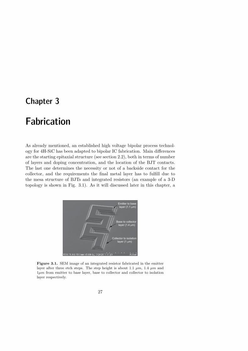
As already mentioned, an established high voltage bipolar process technol-ogy for 4H-SiC has been adapted to bipolar IC fabrication. Main differencesare the starting epitaxial structure (see section 2.2), both in terms of numberof layers and doping concentration, and the location of the BJT contacts.The last one determines the necessity or not of a backside contact for thecollector, and the requirements the final metal layer has to fulfill due tothe mesa structure of BJTs and integrated resistors (an example of a 3-Dtopology is shown in Fig. 3.1). As it will discussed later in this chapter, a
Emitter to base
layer (1.1 µm)
Base to collector
layer (1.4 µm)
Collector to isolation
layer (1 µm)
Figure 3.1. SEM image of an integrated resistor fabricated in the emitterlayer after three etch steps. The step height is about 1.1 µm, 1.4 µm and1µm from emitter to base layer, base to collector and collector to isolationlayer respectively.
27

28 CHAPTER 3. FABRICATION
Sacrificial
oxidation and
passivation
SiC etch
over-etch 1
SiC etchover-etch 2
Collector
lithography
3 Collector definition
over-etch 3
4 n-contact
n-contact
lithography
5 p-contact
p-contact
lithography
Oxide
dry etch
Oxide
deposition,
via holes
lithography
6 Via holes definition
Thick
metallization
deposition and
lithography
Metal
etch
7 Contact and interconnect
definition
1 Emitter definition
EmitterBase
Collector
Isolation Layer (p)
Substrate (n)
Emitter
lithography
1.
2.
3.
4.
8.
10.
11.
12.
13.
14.
15.5.
6.
7.
EmitterBase
Collector
Isolation Layer (p)
Substrate (n)
EmitterBase
Collector
Isolation Layer (p)
Substrate (n)
EmitterBase
Collector
Isolation Layer (p)
Substrate (n)
EmitterBase
Collector
Isolation Layer (p)
Substrate (n)
EmitterBase
Collector
Isolation Layer (p)
Substrate (n)
EmitterBase
Collector
Isolation Layer (p)
Substrate (n)
EmitterBase
Collector
Isolation Layer (p)
Substrate (n)
EmitterBase
Collector
Isolation Layer (p)
Substrate (n)
EmitterBase
Collector
Isolation Layer (p)
Substrate (n)
EmitterBase
Collector
Isolation Layer (p)
Substrate (n)
EmitterBase
Collector
Isolation Layer (p)
Substrate (n)
EmitterBase
Collector
Isolation Layer (p)
Substrate (n)
SiC etch
Base
lithography
2 Base definition
EmitterBase
Collector
Isolation Layer (p)
Substrate (n)
Oxide ecthing,
metal contact
deposition and
annealing
Oxide ecthing,
metal contact
deposition and
annealing
9.
EmitterBase
Collector
Isolation Layer (p)
Substrate (n)
Figure 3.2. IC technology process flow. Required masks are reported alongthe flow (bold text). Color legend: blue indicates photoresist, grey SiO2 andblack metal. Film thicknesses are not drawn to scale.
good step coverage of the final metal layer is essential to make the circuitswork. Two 2-inch wafers have been processed in this work. The 8 off-axis4H-SiC substrates have been purchased from SiCrystal [26], whereas the sixepitaxial layers (n++/n+/p/n−/n++/p) have been grown by Acreo [27] ina continous run in order to minimize interface defects. The process flowused in this work is summarized in Fig. 3.2. It involves seven different

3.1. WAFER CLEANING 29
Table 3.1. Standard chemicals used for surface preparation of SiC wafers.
Description Chemicals / ratio Temperature/Time Removals
RCA SC1 H2O : NH4OH : H2O2 80-90 C Organic
5:1:1 10 min
RCA SC2 H2O : HCl : H2O2 80-90 C Ionic/Metal
5:1:1 10 min
Seven up H2SO4 : H2O2 90-110 C Organic /Metal
3:1 5 min
IMEC H2O :HF : C3CH(OH)CH3H 25 C Oxide
100:1:1 100 sec
Aqua regia HCl : HNO3 50 C Metal
3:1 5 min
Dilute HF HF : H2O 25 C Oxide
1:10
BHF HF : NH4F 25 C Oxide
1:7
masks (emitter layer, base layer, collector layer, n-type contact, p-type con-tact, via and first metal level), and several main processes: wafer cleaning,lithography, SiC etching, oxidation and oxide deposition, and metallization.
3.1 Wafer cleaning
In order to reduce the uncertainty in the process and to get better resultsfrom the successive process steps the surface cleaning of SiC wafer is veryimportant. It basically consists in removing organic or non-organic contam-ination, native oxide or residuals from previous process steps in particularbefore oxide deposition or metallization. Different cleaning techniques areavailable, dry or wet. Concerning the dry cleaning techniques usually hy-drogen or oxygen-plasma are used to physically remove residuals of previousprocess steps, such as hardened photo-resist. Concerning the wet cleaningstandard recipes are given in table 3.1. For fabricating SiC ICs Seven-upand IMEC has been used before thermal oxidation or lithography for SiCetching, and BHF for removing native oxide before metallization. RCA SC1

30 CHAPTER 3. FABRICATION
Figure 3.3. 4-inch Si carrier wafer with a hole in the center. A DSW8500/2035 g-line 5:1 stepper. (Left-right). [28]
and SC2 has been applied, if needed, after SiC etching.
3.2 Lithography
Seven lithography steps have been required to fabricate discussed SiC ICs.Standard high precision stepper lithography with resolution of 1 µm couldbe performed due to the large features of the components designed in thiswork. A DSW 8500/2035 g-line 5:1 stepper has been used (Fig. 3.3) withthe 2-inch SiC substrate placed on a 4-inch Si carrier wafer since the machineis calibrated to 4-inch Si process technology. This requires extra alignmentsteps for adequate accuracy.
3.3 SiC etching
SiC etching is required to fabricate the mesa structures that define the BJTregions and the integrated resistors. Dry techniques, such as reactive ionetching (RIE) or inductively coupled plasma etching (ICP), are usually ap-plied for etching SiC since wet etch is difficult to control because of itsanisotropic property and the high temperature required (> 350 C) due tothe strong bond between Si and C.In this work plasma etching in HBr and Cl2 with a photo-resist mask hasbeen used to form emitter, base, and collector mesas. Applied etching recipe

3.4. OXIDATION AND OXIDE DEPOSITION 31
has been selected since giving rise to sloped sidewalls1 it reduces require-ments for step coverage of the final metal layer.
3.4 Oxidation and oxide deposition
Unlike other wide bandgap materials SiC process provides possibility tothermally grow silicon dioxide (SiO2) beside to deposit it. Thermally grownSiO2 is usually used as sacrificial layer to remove impurities and surfacedamage, or as passivation layer for SiC devices.In this work after the three required etch steps a sacrificial oxidation inN2O ambient has been applied in order to reduce possible damage causedduring the etching. Thus surface passivation has been performed with 50 nmPECVD SiO2 followed by post oxide anneal in N2O at 1150 C for 3 hours[29] in order to minimize surface recombination. A 2µm thick PECVD SiO2
layer has been deposited as intermediate dielectric after contact definitionand prior to the final metal layer deposition.
3.5 Metallization
In SiC process technology for ICs different metallization techniques have tobe considered according to their different purposes: ohmic contact to SiCand interconnect formation. Metallization usually requires surface cleaningand metal deposition followed by patterning or patterning followed by metaldeposition (in case of lift-off process). The formation of good ohmic contactsrequires that the metal is placed in intimate contact with the semiconductor.Therefore all residual oxide, photo-resist or metal contaminations have tobe removed from the semiconductor surface, and a high temperature (≈800C - ≈1000 C) annealing has to be performed in an oxygen free ambientin order to foster a reaction between metal and SiC, and to form silicide incase of Ni contact. However, a too high annealing temperature can deteri-orate the passivation layer. Different deposition techniques can be used inthe metallization process: sputtering, thermal or electron beam evaporationor CVD technique. The sputtering provides a good adhesion of the metal
1Although a fine tuning of the sidewall angle is not required, a few tests have beenperformed aiming to achieve a good compromise between sidewall slope and etch rateuniformity on 2-inch wafer. Basically two gas sets have been tested (SF6 and HBr - Cl2)with different gas flows and power settings.

32 CHAPTER 3. FABRICATION
(a)
(c)
(b)
(d)
Figure 3.4. SEM image showing metalization issues. (a)-(b) Poor stepcoverage [11]. (c)-(d) Significant undercut.
to the substrate but having a good step coverage it can be problematic forlift-off process. In this case evaporation is usually preferred, although it maysuffer of poor adhesion to the substrate. For IC fabrication quality of ohmiccontacts and interconnects is very important for high performance devicesand circuits, and to reduce the power loss.In this work both evaporation and sputtering technique have been used.E-beam evaporation has been used to deposit Ni for emitter and collectorcontacts, and to deposit a triple layer of Ni/Ti/Al with the thickness ratioof 0.1/0.15/0.85 for base and isolation-layer contacts [12]. After each metaldeposition, a lift-off process has been used to pattern the contacts, and anannealing step has been performed for 1 min in Ar ambient at 950 C and820 C for n and p type respectively, in order to provide low resistive ohmiccontacts to the epitaxial layer. Sputtering technique has been used to de-

3.5. METALLIZATION 33
posit the metal layer for realizing the interconnects. As mentioned at thebeginning of this chapter, the circuits fabricated in this work require inter-connects able to face up to three step heights of at about 1µm each withoutbreaking or becoming too narrow, which means a good step coverage and agood control of the undercut during the metal each have to be achieved. Ex-amples of too poor step coverage and too big undercut are shown in Fig. 3.4(a)-(b) and (c)-(d) respectively. The first two refer to a work from anothergroup, while the last two are from this work. They show the interconnectsafter deposition and patterning of a 3 µm thick Al layer. Since these inter-connects were too narrow to make the circuits work, a further 0.5 µm thickAl layer has been sputtered and then patterned just as the previous one.


Chapter 4
Measurement results and
performance evaluation
This chapter mainly presents experimental results obtained in the first ICbatch, focusing on integrated resistors, low voltage NPN and circuit per-formance [PAPER II-III]. It also discusses a study aiming to characterizelateral PNP transistors fabricated in the high voltage technology [PAPERI]. Although PNP transistors have been fabricated in the first IC batch withdifferent finger widths and in different configurations (see 2.4.2) they havenot yet been characterized and due to difficulties occurred during the baselayer etching some of the PNPs exhibit shorted collector and emitter fingers.For both high voltage and IC batch measurement results discussed in thischapter are related to a single 2-inch 4H-SiC wafer.For the HV batch the maximum temperature at which measurements havebeen performed is 200 C, whereas for the IC batch it is 300 C. In the lastcase the maximum temperature is due to limitations of the measurementset-up and not to failure of devices or circuits.
4.1 Active and passive device performance
4.1.1 PNP transistor
A top view image of the investigated 4H-SiC lateral PNP is shown in Fig.4.1 (a). It has been fabricated together with high voltage NPN transistorsby using a high voltage NPN process technology [13]. Doping concentrations
35

36CHAPTER 4. MEASUREMENT RESULTS AND PERFORMANCE
EVALUATION
(a)
Emitter Contact
Base
Contact
Collector Contact
N- Collector
ND = 6 x 1018cm-3
P Base NA = 4.3 x 1017cm-3
N+ Emitter
ND = 6 x 1018cm-3
ND = 4 x 1019cm-30.2µm
1.35µm
0.65µm
25µm
3µm2µm 4µm 6µm
Substrate
Collector
Contact
Base Contact
Emitter
Contact
5µm
WE W
C
NPN PNP
E
C
simulated
sectionnarrower finger
(14µm)
wider finger
(20µm)
(b)
Figure 4.1. PNP transistor fabricated in a high voltage technology. (a) -Cross section. (b) - Top view optical image.
and thicknesses of each layer are summarized in the cross-sectional view ofthe 20 µm half pitch PNP shown in Fig. 4.1 (b). The top terminals havebeen named collector and emitter after measuring the structure in orderto guarantee a forward current gain higher than the reverse one. SevenPNPs located in different dies on the same wafer have been characterizedat 27 C by the means of forward and reverse Gummel plots and outputcharacteristics. Measured current gains, as well as those predicted by devicesimulations performed by using Sentaurus TCAD [19] (see PAPER I fordetails), are extremely low as shown in Fig. 4.2. Measured current gainsrange from 0.007 to 0.013 when the narrower fingers act as emitter and from0.005 to 0.009 when they act as collector. Although significant variationsaffect the measured gains (see Fig. 4.2), they all exhibit the same behaviorthat is similar to that predicted by device simulations: the current gain ishigher when the narrower fingers act as emitter. Based on this result thetop terminal connected to the narrower fingers has been named emitter,and the other one collector. Device simulations show that the differencebetween βF and βR is due to the asymmetrical geometry of the device:using the narrower fingers as emitter both the effective base width and thebase current decrease, which makes βF bigger due to the smaller amount ofholes that injected from the emitter into the base diffuse towards the basecontact. However, characterization of PNPs fabricated in the first IC batch1
1As mentioned in 2.4.1 PNPs with different geometries are available.

4.1. ACTIVE AND PASSIVE DEVICE PERFORMANCE 37
10−6
10−5
10−4
10−3
10−2
0
0.005
0.01
0.015
IC [A]
β F
# 1# 2# 3# 4
# 5# 6# 7
Simulated
# 1# 2# 3# 4
# 5# 6# 7
Simulated
10−6
10−5
10−4
10−3
10−2
IE [A]
0
0.005
0.01
0.015
β R
(a) (b)
Figure 4.2. Simulated and measured current gains (on seven PNP transis-tors) at 27 C. (a) Forward current gain. (b) - Reverse current gaoin.
β=62
β =0.016
NPN and PNP
β=0.016
PNP
B
B
E
E
C
C
0 2 4 6 8 100
4
8
12
16
−VCE [V]
IC [m
A]
IB=5mA/step
(b)10 −10 10 −5 100
0
0.2
0.4
0.6
log 10( IC ) [A]
βF
VBC=6V
(a)Simulated PNP and NPN
10−8
10−6
10−4
10−2
0
0.01
0.02
Measured PNP
0 2 4 6 8 100
0.2
0.4Measured PNP
Simulated PNP and NPN
(c)
Figure 4.3. SPICE simulation results for Sziklay configuration (dashedlines) and the lateral PNP (♯ 2 in Fig. 4.2) measurement results (solid lines).(a) - Forward current gain vs. collector current. (b) - Collector currentvs. emitter-collector voltage. (c) - Single PNP (top), Sziklay configuration(bottom).
is necessary to confirm this thesis since PNPs with different emitter andcollector finger widths are available. In order to improve the performanceof the fabricated PNP a Sziklay configuration built with one NPN, with ahigh current gain, and one PNP (see Fig. 4.3 (c)) has been tested by themeans of LTspice simulations. To this end SPICE models extracted with theprocedure illustrated in section 2.1 have been used for one of the fabricatedlateral PNPs (♯2 in Fig. 4.2) and a large area NPN transistor (size 300µm×
300 µm) with βF equal to 62 fabricated on the same wafer. SPICE models

38CHAPTER 4. MEASUREMENT RESULTS AND PERFORMANCE
EVALUATION
(a) (b) (c)
(d)
Figure 4.4. Optical image of the test structures fabricated in the emitterlayer in order to characterize the integrated resistors. (a) - strip and ser-pentine isolated integrated resistors with different sizes: strip resistors 8 µmwide (1, 5, 10, 15, 20 and 25 squares) and 26 µm wide (5 and 10 squares),and 10 and 20 square serpentine resistors. (b) - TLM structures. (c) - Kelvinstructures.
are summarized in PAPER I. Simulated forward output characteristic andcurrent gain for the Sziklay configuration are shown in Figs. 4.3 (a) and(b). The equivalent PNP transistor exhibits an emitter-collector voltage(VEC) in forward conduction increased by the voltage drop of the NPN base-emitter junction and a βF of 0.6 instead of 0.013 measured for the fabricatedPNP, which means an increase of a factor 37 could be achieved. It is worthnoticing that βF larger than 0.6 could be reached for the equivalent PNP byoptimizing the areas of the PNP and the NPN in order to have both devicesoperating simultaneously at the maximum gain. In fact in the characteristicsshown in Fig. 4.3 the NPN is not operated at its maximum current gainsince the current density is too small.
4.1.2 Integrated resistors
Fig. 4.4 shows an example of the test structures fabricated in emitter, baseand collector layer in order to characterize the integrated resistors. Theyconsist of TLM structures, contact chain, kelvin structures and isolated

4.1. ACTIVE AND PASSIVE DEVICE PERFORMANCE 39
0 5 10 15 20 250
1
2
3
Number of squares
Re
sis
tan
ce
[kΩ
]
Emitter layer
0 5 10 15 20 25
Number of squares
0
0.5
1
1.5
Re
sis
tan
ce
[M
Ω]
Base layer
0
1R
esis
tan
ce
[kΩ
]
3
2
4
5 10 15 20 25
Number of squares
Strip IRs (8µm wide)
Serpentine IRs
Strip IRs (26µm wide)
Strip IRs (8µm wide)
Serpentine IRs
Strip IRs (26µm wide)
Strip IRs (8µm wide)
Serpentine IRs
Strip IRs (26µm wide)
Collector layer
(a) (b) (c)
Figure 4.5. Measurement results for test integrated resistors at 27 C indifferent layers. (a) - Emitter layer. (b) - Base layer. (c) - Collector layer.The dashed lines show the linear fit of the resistances measured for the 8µm wide strip resistors.
integrated resistors with two contact pads for each terminal. At 27 C TLMmeasurements have been performed on 9 different dies, whereas the isolatedresistors have been tested in only one die for each layer [30].
At 27 C the mean values of emitter and collector sheet resistance are 115and 174 Ω/square respectively, in accordance with layer doping and thick-ness. However, the average base sheet resistance, measured as 55 kΩ/square,is higher than what was expected. Measured sheet resistance exhibits a cer-tain variation in emitter and base layers, where it ranges between 73 and140 Ω/square and between 43 and 67 kΩ/square respectively, unlike inthe collector layer where it ranges between 164 and 187 Ω/square. Severalcauses can determine such variation: nonuniform doping concentration andthickness of the epitaxial layers, nonuniform SiC etch rate and so on. Spe-cific contact resistivity has been measured as 1.7 × 10⁻⁵, 7.5 × 10⁻⁶ and5.0 × 10−4 Ω · cm2 for emitter, collector and base layer respectively.A four point probe method has been used to measure the resistances of eightstrip resistors with different sizes and widths and 2 serpentine resistors. Mea-surement results collected in Fig. 4.5 for all the three layers are coherentwith designed geometry and parameters extracted from the TLM measure-ments. It is worth noticing that in few cases contact resistances higher thanwhat was expected have been observed due to difficulties occurred duringohmic contact formation. Sheet resistance and specific contact resistance

40CHAPTER 4. MEASUREMENT RESULTS AND PERFORMANCE
EVALUATION
Table 4.1. TLM measurement results in emitter, base and collector layerin the same die in the temperature range 27 - 300 C.
Parameters Temperature (C) Emitter Base Collector
27 87 59×103 162
Sheet 50 85 48×103 156
resistance 100 82 32×103 147
(Ω/square) 150 79 27×103 144
200 81 24×103 144
250 82 24×103 150
300 88 23×103 157
27 5.3 1.2 3.1
Transfer 50 5.2 1.0 3.2
length 100 5.1 1.2 3.1
(µm) 150 5.3 0.8 3.1
200 4.9 0.9 2.9
250 4.9 0.7 2.6
300 4.4 0.7 2.4
27 2.5×10⁻⁵ 8.4×10⁻⁴ 1.6×10⁻⁵
Specific 50 2.3×10⁻⁵ 4.5×10⁻⁴ 1.6×10⁻⁵
contact 100 2.1×10⁻⁵ 5.0×10⁻⁴ 1.5×10⁻⁵
resistivity 150 2.2×10⁻⁵ 1.5×10⁻⁴ 1.3×10⁻⁵
(Ω·cm2) 200 1.9×10⁻⁵ 1.8×10⁻⁴ 1.2×10⁻⁵
250 2.0×10⁻⁵ 1.1×10⁻⁴ 1.0×10⁻⁵
300 1.7×10⁻⁵ 1.1×10⁻⁴ 0.9×10⁻⁵
of the emitter layer in the IC technology are compatible with those in thehigh voltage technology, which have been used to derive the geometrical di-mensions of the integrated resistors as discussed in section 2.4.2. Therefore,designed and obtained resistance values are expected to be close.The temperature behavior of sheet resistance and specific contact resistancehas been evaluated in the range 27 - 300 C for all the three layers in only onedie. Measurement results are given in table 4.1. Both emitter and collectorsheet resistance show non-monotonous temperature dependences, whereasthe base sheet resistance decreases for increasing temperature. Emitter andcollector specific contact resistances do not exhibit significant variation in

4.1. ACTIVE AND PASSIVE DEVICE PERFORMANCE 41
0 100 200 30020
25
30
35
40
45
50
NPN # 1NPN # 2NPN # 3NPN # 4NPN # 5NPN # 6
Temperature [°C]
simulated
Fo
rwa
rd C
urr
en
t G
ain
VBC = 0 V
Emitter Contact
Base
Contact
Base
Contact
Collector
Contact
n-type substrate
N+ Collector ND = 1 x 1019cm-3
N- Collector ND = 1 x 1016cm-3
P Base NA = 1.4 x 1018cm-3
N+ Emitter
ND = 1 x 1019cm-3
ND = 3 x 1019cm-30.2µm
0.8µm
0.3µm
1µm
1µm
2µm P isolation layer NA = 1.4 x 1018cm-3
30µm35µm 35µm 60µm
Emitter
Collector Base
(a) (b) (c)
100µm
17µm
Figure 4.6. Low voltage NPN transistor. (a) - Cross section. (b) - Opticalimage. (c) - Measured (on six NPNs) and simulated forward current gainvs. temperature in the range 27-300 C .
the considered temperature range, unlike the base specific contact resistancethat has been found to be decreasing with temperature by about 22%.
4.1.3 Low voltage NPN transistor
Six NPN transistors have been characterized up to 300 C (PAPER II).For all the devices measured current gain drops from about 46 at 27 C to21 at 300 C, as predicted by 2-D simulations performed with SentaurusTCAD [19] (see Fig. 4.6 (c)), where model parameters used in the devicesimulations discussed in section 2.2 have been adjusted in order to matchmeasurements with simulated NPN characteristics. When the temperaturegoes from 27 up to 100 C βF decreases faster than for further increasingof the temperature. A simple fitting of the Arrhenius plot of the measuredcurrent gain vs. temperature (β vs. 1/T ) allows to extract a current gain ofabout 10 at 600 C. Although this is too low to allow operation of analoguecircuits it is high enough to permit that of digital ones. At each temperaturethe current gain abruptly drops at high collector current (IC), as shown bymeasured and simulated Gummel plot and the βF vs. VBE at 27 C depictedin Fig. 4.7 (a). The current gain reaches its maximum value of 45 at IC =20 mA and drops for higher collector current because of high injection in thelow doped collector and forward biasing of the base collector junction. Thelatter is the main reason for the gain reduction according to the Gummel

42CHAPTER 4. MEASUREMENT RESULTS AND PERFORMANCE
EVALUATION
10−8
10−6
10−4
10−2
1
3 4
50
2.5 3.5
0
10
20
30
40
I B NPN #1
β
IC NPN #1
NPN #1
IB sim.IC sim.b sim.
VBE [V]
I B, I C
[A
]
Fo
rwa
rd C
urre
nt G
ain
VBC= 0 VT = 27 °C
3 42.5 3.5
T = 27 °C
4.5
50
10
30
10-8 10-4Fo
rwa
rd C
urr
en
t G
ain
IC [A]100
T = 27 °C
VBC = 0V
VCE = 6V
VCE = 8V
VCE
VCE
10−8
10−6
10−4
10−2
I B, I C
[A
]
VBE [V]
IB at VBC = 0V
IB at VCE = 6V
IB at VCE = 8V
IC at VCE = 8V
IC at VBC = 0V
IC at VCE = 6V
(a) (b)
Figure 4.7. Forward Gummel plot and current gain at 27 C. (a) Mea-surement and simulation results at VBC = 0V . (b) Measurement results atVBC = 0 V , and VCE = 6 V and VCE = 8 V
plot. When the base-emitter voltage approaches 3.5 V and IC is about 20mA IB increases while the gain drops. Furthermore Gummel plots measuredat different fixed VCE show a delay in the onset of BJT saturation, and soin the gain drop, proportional to the reverse voltage applied to the basecollector junction. The Gummel plots measured at fixed VCE equal to 6and 8 V and at fixed VCE = 0 V are shown in Fig. 4.7 (b). However, nosignificant variations have been observed in the maximum βF as shown in theinset in Fig. 4.7 (b). Device saturation is caused by the collector resistanceof the NPN, and in particular by the lateral flow of IC in the heavily dopedcollector layer, which constitutes the major contribution to the collectorresistance. Despite the high doping concentration (1 × 1019 cm−3, see 4.6(a)) the resistance seen by the collector current is significant because of therelatively small thickness of the layer and the device geometrical dimensions.In fact the collector resistance, evaluated from the initial slope of the outputcharacteristic depicted in Fig. 4.8 (a), is about 150 Ω. It could be possible toreduce the collector resistance by rescaling the device size and in particularby reducing the distance between base layer edge and collector contact edge(see Fig. 4.6 (b)), which is 17 µm wide. This distance has been designedresponding to circuit layout issues rather than device performance. It islarge enough to be crossed by an interconnection line in order to reducethe restrictions deriving from the use of a single metal layer. Although

4.1. ACTIVE AND PASSIVE DEVICE PERFORMANCE 43
0 2 4 6 80
10
20
30
40
VCE [V]
I C [m
A]
IB step 0.2mA
T=27 °C
NPN #1NPN #2NPN #3NPN #4NPN #5NPN #6sim.
T=200 °C
0 2 4 6 80
10
20
30
40
VCE [V]
I C [m
A]
IB step 0.2mA
T=300 °C
IB step 0.2mA
0 2 4 6 80
10
20
30
40
VCE [V]
I C [m
A]
T=100 °C
IB step 0.2mA
0 2 4 6 80
10
20
30
40
VCE [V]
I C [m
A]
(a) (b)
(c) (d)
Figure 4.8. Low voltage NPN transistor: measured (on six NPNs, shownin solid lines) and simulated (stars) output characteristic at different tem-peratures. (a) - 27 C. (b) - 100 C. (c) - 200 C. (d) - 300 C.
at each temperature almost no variation has been found in βF a certainvariation has been observed in the collector resistance of different transistors.This is evident in Fig. 4.8, which depicts measured and simulated outputcharacteristics at 27, 100, 200 and 300 C. Furthermore a non-monotonousbehavior has been observed for the specific on-resistance. It first decreasesfrom 14 mΩ · cm2 to 11 mΩ · cm2 when the temperature rises from 27 Cup to 200 C and then increases again to 12 mΩ · cm2 at 300 C, followingthe behavior of the n+ collector sheet resistance. As already noticed thecontribution to the collector resistance coming from the high doped collectorlayer, where the current flows laterally, dominates over the contribution dueto the vertical current flow in the n− collector layer.

44CHAPTER 4. MEASUREMENT RESULTS AND PERFORMANCE
EVALUATION
4.2 Circuit performance
Although different circuits have been designed and fabricated only thosealready characterized will be discussed in this chapter, which means theOR-NOR gate and the 3-stage ring oscillator [PAPER II] [PAPER III]. Con-cerning the OR-NOR gate, its performance has been evaluated by estimatingnoise margins2 (NMs), power loss3 and propagation delay4 (TP ). Althoughthese parameters are usually evaluated for a basic inverter in order to char-acterize the performance of a logic-circuit family [23], in this work they havebeen estimated for both outputs of the OR-NOR gate. Furthermore, NMsand static power loss (PD) have been evaluated at different temperatures upto 300 C, whereas TP has been measured at 27 C. An estimation of TP ofa single gate up to 300 C has been achieved by using the ring oscillator.
4.2.1 OR-NOR gate
DC measurements have been performed by applying the input signal, sweptbetween -9 and 0 V, at one input (A or B in figure 4.9 (a)) leaving the otherone open. Due to the connection to VEE through the pull-down resistor(Ri1 or Ri2) a disconnected input terminal has a low voltage level appliedto it. Measured VTCs at 27, 100, 200 and 300 C for three different gatestogether with estimated noise margins are shown in Fig. 4.10 for OR andNOR output respectively when -15 V supply is applied. Both measured highand low voltage levels, as well as the logic threshold and their temperaturebehavior, are in good agreement with simulation results (see section 2.3)and do not exhibit significant variation. OR and NOR noise margins arestable from 27 up to 300 C: OR NMH and NOR NML are about 1.1 V,whereas OR NML is about 0.9 V, only NOR NMH slightly decreases whenthe temperature increases from 0.9 V at 27 C to 0.8 V at 300 C (PAPERII). Although the collector resistance of the low voltage transistor, which hasnot been taken into account for designing and simulating the gate, is equal
2The NMs have been already defined in 2.3.3It usually accounts for both static and dynamic power dissipated in a single gate.4It characterizes the dynamic performance of a logic-circuit family. The shorter it
is the highest the speed at which the circuit can be operated. It is defined as the timeelapsed between the input and the output signal transitions, and it is measured at halfof the logic swing (difference between high and low voltage levels). It is defined for boththe transitions of the output signal: low-to-high (TP LH) and high-to-low (TP HL). Theirmean value gives the propagation delay TP .

4.2. CIRCUIT PERFORMANCE 45
Vref
GND
A
Vout (NOR)
Vout (OR)
VEE= -15V
Q7
R1aQ5
RC2
Q10
Q8
R1b
Ree
Q6
Ri2
Q1
Rout1
Reb
Ri1Q4
Q2
Rout2
Q3
R2
RC1
Q9
Differential
input stage
Reference
voltage
generator
Output
stage
B
100µm
100Ω(103Ω)
10KΩ(11.3KΩ)
10KΩ(11.3KΩ)
330Ω(362Ω)
700Ω(827Ω)
3.7KΩ(4.2KΩ)
3.8KΩ(4.3KΩ)
8KΩ(9.1KΩ)
500Ω(556Ω)
(a) (b)
Figure 4.9. ECL OR-NOR gate. (a) - Circuit diagram with designed andfabricated (in brackets) resistance values. (b) - Optical image.
−6 −5 −4 −3 −2
−5
−4
−3
T=27°C
T=100°C
T=200°C
T=300°C
T
VIN [V]
gate # 1
gate # 2
gate # 3
0 100 200 3000.8
1
1.2
NMH
NML
NM
[V
]
Temperature [°C]
VEE = -15 V
VO
R [V
]
−8 −6 −4 −2 0
−5
−4
−3
T
VN
OR
[V
]
VIN [V]
T=27°C
T=100°C
T=200°C
T=300°C
gate # 1
gate # 2
gate # 3
VEE = -15 V
0.75
0.95
1.15
NM
[V
]
Temperature [°C]
NMH
NML
0 100 200 300
(a) (b)
Figure 4.10. Measured VIN −VOUT characteristics on three OR-NOR gatesat 27, 100, 200 and 300 C; the insets show the noise margins vs temperature.(a) - OR output. (b) - NOR output.

46CHAPTER 4. MEASUREMENT RESULTS AND PERFORMANCE
EVALUATION
Table 4.2. Designed and experimental resistance values (given in Ω) forOR-NOR gate ♯1 in Fig. 4.10, where the experimental values are thoseestimated from measured sheet resistance and specific contact resistivity inthe same die at 27 C.
Resistance value R1a R1b Ree Reb Rc1 Rc2 Rout R2
Designed 100 330 8000 500 3700 3800 10000 700
Experimental 103 362 9060 556 4188 4316 11341 827
−7 −5 −3
−7
−5
−3
VN
OR
, V
IN [V
]
VIN, VNOR [V]
T = 27 °C
VEE
VEE = -7 V
VEE = -15 V
VEE = -20 V
T = 27 °C
VEE
VEE = -7 V
VEE = -15 V
VEE = -20 V
−7 −5 −3−7
−5
−3
VO
R, V
IN [V
]
VIN, VOR [V]
VO
R, V
IN [V
]
VIN,VOR [V]−3.5
−2.8
−3.5−2.8
(a) (b)
Figure 4.11. Measured voltage transfer characteristics at VEE = −7, −15and −20 V . (a) - OR output. (b) - NOR output.
to 150 Ω at room temperature (see section 4.1.3), it has no significant effecton the OR-NOR behavior due to the used circuit design. All the transistorshave the collector terminal connected to ground or to a resistor with a muchbigger resistance value. It is worth noticing that for the characterized OR-NOR gates the biggest variation between designed and estimated resistancevalues is about 18%. Calculations have been based on resistor dimensionsand sheet and contact resistance measured in the same die. Both resistancevalues are given in table 4.2 and in Fig. 4.9 for all the resistors of the OR-NOR gate referred as ♯1 in Fig. 4.10. At 27 C the logic gate ♯1 has been
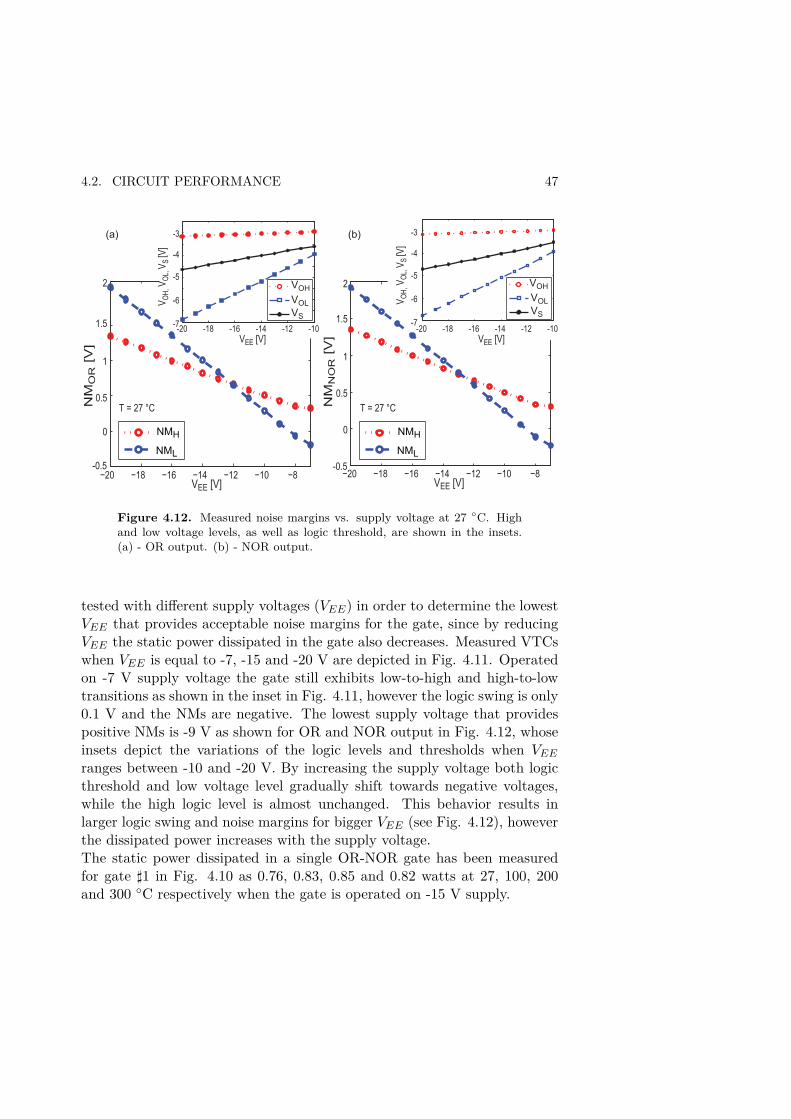
4.2. CIRCUIT PERFORMANCE 47
0
0.5
1
1.5
2
-0.5−20 −18 −16 −14 −12 −10
VEE [V]
NM
NO
R [
V]
−8
NMH
NML
T = 27 °C
NMH
NML
−20 −18 −16 −14 −12 −10VEE [V]
NM
OR [
V]
T = 27 °C
−8
-18 -16 -14 -12 -10VEE [V]
-7
-6
-5
-4
-3
-20
VO
H, V
OL,
VS
[V]
VOH
VOL
VS
-7
-6
-5
-4
-3
-20 -18 -16 -14 -12 -10VEE [V]
VO
H, V
OL,
VS
[V]
VOH
VOL
VS
0
0.5
1
1.5
2
-0.5
(a) (b)
Figure 4.12. Measured noise margins vs. supply voltage at 27 C. Highand low voltage levels, as well as logic threshold, are shown in the insets.(a) - OR output. (b) - NOR output.
tested with different supply voltages (VEE) in order to determine the lowestVEE that provides acceptable noise margins for the gate, since by reducingVEE the static power dissipated in the gate also decreases. Measured VTCswhen VEE is equal to -7, -15 and -20 V are depicted in Fig. 4.11. Operatedon -7 V supply voltage the gate still exhibits low-to-high and high-to-lowtransitions as shown in the inset in Fig. 4.11, however the logic swing is only0.1 V and the NMs are negative. The lowest supply voltage that providespositive NMs is -9 V as shown for OR and NOR output in Fig. 4.12, whoseinsets depict the variations of the logic levels and thresholds when VEE
ranges between -10 and -20 V. By increasing the supply voltage both logicthreshold and low voltage level gradually shift towards negative voltages,while the high logic level is almost unchanged. This behavior results inlarger logic swing and noise margins for bigger VEE (see Fig. 4.12), howeverthe dissipated power increases with the supply voltage.The static power dissipated in a single OR-NOR gate has been measuredfor gate ♯1 in Fig. 4.10 as 0.76, 0.83, 0.85 and 0.82 watts at 27, 100, 200and 300 C respectively when the gate is operated on -15 V supply.

48CHAPTER 4. MEASUREMENT RESULTS AND PERFORMANCE
EVALUATION
−10 -8 -6 -4 -2 0 2 4 6 8 10−6
−5
−4
−3
Time [ms]
Vin
Vout
Vin
, V
OR
[V
]
TPHL=
420ns
tf=660nstr=240ns
TPLH=
130ns
(a)
Vin
, V
NO
R [V
]
TPHL=
390ns
tf=690nstr=400ns
TPLH=
210ns
(b)
−10 -8 -6 -4 -2 0 2 4 6 8 10−6
−5
−4
−3
Time [ms]
Vin
VoutT = 27 °C
VEE = -15VT = 27 °C
VEE = -15V
Figure 4.13. OR-NOR gate: preliminary switching measurements at 27C for gate ♯1 in Fig. 4.10. (a) - OR output. (b) - NOR output.
Preliminary switching waveforms of the OR-NOR gate (♯1 in Fig. 4.10) atroom temperature are shown in Fig. 4.13. The measurements have beenperformed at T = 27 C and VEE = -15 V, with a peak-to-peak inputvoltage of about 2.5 V centered about the logic threshold. Both the ORand NOR outputs exhibit asymmetric low-to-high (TP LH) and high-to-low(TP HL) propagation delays. The average propagation delay (TP ) is about280 ns and 320 ns for OR and NOR output respectively. Propagation delays,as well as rise and fall time, for both the outputs are shown in Fig. 4.13. Abetter estimation of the propagation delay achievable by the reported ECLtechnology is the one measured using the fabricated ring oscillator.
4.2.2 Ring oscillator
An optical image of the fabricated ring oscillator is shown in Fig. 4.14.Although three stages are enough to make it oscillate, thanks to a logic swingof the fundamental gate equal to about 2 V [31], the resulting oscillationperiod is not always long enough to allow each gate to settle the nominalhigh or low output voltages. This phenomenon is shown in Fig. 4.15, whichcollects the output characteristic of the ring oscillator at 27, 100, 200 and300 C and VEE = -15 V. At 27 C the measured logic swing of the ringoscillator is about 0.7 V whereas its maximum value, equal to half of the logicswing of the basic gate [31], is about 0.8 V and the oscillation frequency isabout 1.6 MHz, which results in a stage delay of about 105 ns. The reduced

4.2. CIRCUIT PERFORMANCE 49
Stage 1
Feedback
Stage 2 Stage 3 Stage 4
A
VEE
GND
OUT 250µm
Fundamental gate
Figure 4.14. 3-stage ring oscillator: optical image.
−3.6
-0.4 −0.2 0 0.2 0.4
Time [ms]
−4.0
−4.4
T = 27 °C
fosc= 1.57 MHz
−4.2
−4.4
−4.6 T = 200 °C
fosc= 2.77 MHz
−4.2
−4.6
−4.8
T = 300 °C
fosc= 2.67 MHz
−3.8
−4.0
−4.2T = 100 °C
fosc= 2.2 MHz
VO
UT [
V]
TP = Tosc / 2N
= 62 ns
TP = Tosc / 2N
= 60 ns
TP = Tosc / 2N
= 76 ns
TP = Tosc / 2N = 105 ns
-0.4 −0.2 0 0.2 0.4
Time [ms]
Figure 4.15. 3-stage ring oscillator: time-domain oscillation measurementsat 27 C.
logic swing exhibited at 27 C agrees with measured rise and fall times ofthe NOR output of the fundamental gate, which are larger than half of theoscillation period. Increasing the temperature, reduction of the logic swingand a non-monotonous behavior of TP have been observed (see Fig. 4.15).Measured propagation delays for the fundamental gate are 76, 60 and 62 nsat 100, 200 and 300 C respectively.


Chapter 5
Conclusions and future work
This work deals with 4H-SiC integrated circuits capable of high tempera-ture operation. Different research areas are involved: modeling, simulationas well as design, processing and characterization. A 4H-SiC high voltageNPN process technology has been adapted to integrated circuit fabrication.An elementary design kit has been developed for the resulting 4H-SiC ICtechnology. It is an in-progress design kit that should be improved andenlarged after each IC batch characterization. Up to now it consists of ap-propriate SPICE models for NPN transistors at different temperatures (27and 200 °C) including only DC parameters, and layout cells for test struc-tures and passive and active devices with scalable dimensions, as well asa few basic logic gates. Characterization of the first IC batch showed thesuccessful operation of integrated ECL OR-NOR gates from 27 °C up to300 °C, reported for the first time in PAPER II, with stable noise marginsof about 1 V in the entire temperature range. Furthermore an oscillationfrequency of about 2 MHz has been observed in the same temperature rangefor a 3-stage ring oscillator, consisting of 88 components (40 transistors and48 integrated resistors) and based on the ECL OR-NOR gate, when oper-ated on -15 V supply [PAPER III]. Such performance has been achievedthanks to a temperature compensation network included in the OR-NORcircuit diagram, and the acceptable behavior of the NPN transistors at hightemperature. Although the NPN current gain decreases for increasing tem-peratures, at 300 °C it is still 21.Further work is needed in all the research areas mentioned at the beginningof this chapter (characterization, modeling, simulation and processing) in
51

52 CHAPTER 5. CONCLUSIONS AND FUTURE WORK
order to establish a 4H-SiC IC technology that will allow fabrication of highperformance ICs for high temperature applications. Details about each ofthem are given below:
1. not all the circuits and the test structures fabricated in the first batchhave been characterized: capacitors, analogue circuits, isolated PNPs,Darlington and Sziklay structures (see section 2.4) have not yet beentested. Characterization and modeling of PNPs, Darlington and Szik-lay transistors is fundamental to develop a technology that will makecircuit design easier and more flexible by providing both NPN andPNP transistors.Investigated temperature range will be extended above 300 °C thanksto the recent availability of a hot chuck capable of 600 °C operation.Although the IC batch does not have the same high temperature capa-bility, due to the use of Aluminum in both interconnects and contactmetal stack, it would be interesting to determine at which temperaturemetallization issues compromise the operation of fabricated devicesand circuits.
2. Characterization of transistors and passive devices fabricated in thefirst batch will be used to extract more accurate and complete SPICEmodels for SiC BJTs, and to design resistors and capacitors required tofabricated integrated circuits. At the same time it could be interestingto use such characterization to further develop 4H-SiC models used indevice level simulations, especially for temperatures above 200 °C.
3. Concerning circuit simulation future efforts will focus on improvingthe design of the already fabricated digital and analogue circuits, aswell as on designing new and larger circuits. It could be relevant tofabricate an 11-stage ring oscillator that does not use the fabricatedOR-NOR gate as fundamental gate but NOT gate derived from it. Itscharacterization would allow a better estimation of the propagationdelay of the IC technology, which will not be affected by reduced logicswing and by unused stages (i.e. OR output stages). Furthermoresmaller transistors will be designed and tested in order to improve cir-cuit performance such as occupied area, propagation delay and powerdissipation.

53
4. Concerning the process technology several steps can be improved: SiCetching, passivation and metalization. Different etching systems anddifferent gas chemistry could be tested in order to get a better con-trol of etched thickness and sidewall slope, as well as to improve thesidewall roughness all over the wafer (future batches will use 3 or 4inch wafers). This would allow to achieve higher current gain for NPNtransistors thanks to even thinner base layer, which can be used onlyif a very uniform etching process is available, and high quality emittersidewall. For this purpose different passivation layers could be tested,since several studies showed that it has a strong effect on SiC NPNcurrent gain [29]. Concerning the metallization two-level intercon-nects and different metals, which can withstand higher temperaturethan Aluminum, could be tested and developed in order to simplifycircuit layout and reach higher circuit temperature operation. How-ever, to overcome the temperature limit of the existing IC technologyhigh temperature contacts have to be developed too. This topic willbe investigated in another project related to this work.


Bibliography
[1] P.G. Neudeck, R.S. Okojie, and L.-Y. Chen. High-temperature elec-tronics - a role for wide bandgap semiconductors? Proceedings of theIEEE, vol. 90(6):pp. 1065–1076, 2002.
[2] Carl-Mikael Zetterling. Process technology for silicon carbide devices.Copyright 2003, IEE, London, UK, 2002.
[3] Stephen E. Saddow Anant Agarwal. Advances in silicon carbide pro-cessing and applications. Artech House, Inc., 2004.
[4] Si and SiC parameter references. www.ioffe.ru/SVA/NSM/Semicond/.
[5] Robert F. Pierret. Semiconductor device fundamentals. Addison-WesleyPublishing Company, Inc., 1996.
[6] P.G. Neudeck, S.L. Garverick, D.J. Spry, L.-Y. Chen, G.M. Beheim,M.J. Krasowski, and M. Mehregany. Extreme temperature 6H-SiCJFET integrated circuit technology. Physica Status Solidi (A) Applica-tions and Materials, vol. 206(10):pp. 2329–2345, 2009.
[7] S.-H. Ryu, K.T. Kornegay, J.A. Cooper Jr., and M.R. Melloch. Dig-ital CMOS IC’s in 6H-SiC operating on a 5-V power supply. IEEETransactions on Electron Devices, vol. 45(1):pp. 45–53, 1998.
[8] D.T. Clark, E.P. Ramsay, A.E. Murphy, D.A. Smith, R.F. Thompson,R.A.R. Young, J.D. Cormack, C. Zhu, S. Finney, and J. Fletcher. Hightemperature silicon carbide CMOS integrated circuits. Materials Sci-ence Forum, vol. 679-680:pp. 726–729, 2011.
[9] J.-Y. Lee, S. Singh, and J.A. Cooper. Demonstration and characteriza-tion of bipolar monolithic integrated circuits in 4H-SiC. IEEE Trans-actions on Electron Devices, vol. 55(8):pp. 1946–53, 2008.
55

56 BIBLIOGRAPHY
[10] S. Singh and J.A. Cooper. Bipolar integrated circuits in 4H-SiC. IEEETransactions on Electron Devices, vol. 58(4):pp. 1084–1090, 2011.
[11] Shakti Singh. High-performance TTL bipolar integrated circuits in 4H-SiC. PhD thesis, Purdue University, 2010.
[12] R. Ghandi, H.-S. Lee, M. Domeij, B. Buono, C.-M. Zetterling, andM. Östling. Fabrication of 2700-V 12-mΩcm2 non ion-implanted 4H-SiC BJTs with common-emitter current gain of 50. IEEE ElectronDevice Letters, vol. 29(10):pp. 1135–7, 2008.
[13] R. Ghandi, B. Buono, M. Domeij, C.-M. Zetterling, and M. Östling.High-voltage (2.8 kV) implantation-free 4H-SiC BJTs with long-termstability of the current gain. IEEE Transactions on Electron Devices,vol. 58(8):pp. 2665–2669, 2011.
[14] F. Sischka. Gummel Poon Bipolar model. Agilent Technologies, Munich,1990.
[15] Giuseppe Massobrio and Paolo Antognetti. Semiconductor device mod-eling with SPICE. McGraw-Hill, New York, 2nd edition, 1993.
[16] Switcher CAD III/ LTspice from Linear Technology, available atwww.linear.com/software.
[17] Alessandro Magnani. Electrothermal SPICE modelling for SiC powerbipolar transistors. Master’s thesis, KTH Royal Institute of Technology,ICT, 2009.
[18] Luigia Lanni. SiC bipolar junction transistor for low voltage and hightemperature integrated circuits: design and simulation for a first testchip. Master’s thesis, KTH Royal Institute of Technology, ICT, 2009.
[19] Sentaurus TCAD version 10.0 from Synopsys Inc. available atwww.synopsys.com., 2011.
[20] B. Buono, R. Ghandi, M. Domeij, B.G. Malm, C.-M. Zetterling, andM. Östling. Modeling and characterization of current gain versus tem-perature in 4H-SiC power BJTs. IEEE Transactions on Electron De-vices, vol. 57(3):pp. 704–11, 2010.

BIBLIOGRAPHY 57
[21] B. Buono, R. Ghandi, M. Domeij, B.G. Malm, C.-M. Zetterling, andM. Östling. Influence of emitter width and emitter-base distance on thecurrent gain in 4H-SiC power BJTs. IEEE Transactions on ElectronDevices, vol. 57(10):pp. 2664–70, 2010.
[22] Jr. William R. Blood. MECL System Design Handbook. Scillic, 4thedition, 2000.
[23] Adel S. Sedra and Kenneth C Smith. Microelectronic Circuits RevisedEdition. Oxford University Press, Inc., 5th edition, 2007.
[24] Virtuoso from Cadence, www.cadence.com., 2011.
[25] Paul Horowitz and Winfield Hill. The art of electronics. CambridgeUniversity Press, Cambridge, 2nd edition, 1989.
[26] Sicrystal AG, www.sicrystal.de.
[27] Acreo AB, www.acreo.se.
[28] Hyung-Seok Lee. Fabrication and Characterization of Silicon CarbidePower Bipolar Junction Transistors. PhD thesis, Department of Micro-electronics and Information Technology KTH, Royal Institute of Tech-nology, 2008.
[29] R. Ghandi, B. Buono, M. Domeij, R. Esteve, A. Schöner, J. Han,S. Dimitrijev, S.A. Reshanov, C.-M. Zetterling, and M. Östling.Surface-passivation effects on the performance of 4H-SiC BJTs. IEEETransactions on Electron Devices, vol. 58(1):pp. 259–265, 2011.
[30] Giovanni Fevola. Electrical characterization and modeling of SiC ICtest structures. Master project presentation, KTH Royal Institute ofTechnology, ICT, August 2011.
[31] Massimo Alioto and Gaetano Palumbo. Model and Design of Bipolarand MOS Current-Mode Logic: CML, ECL and SCL Digital Circuits.Springer, 2005.


