
Bipolar Transistors Base Drive Circuits Power MOSFETs Gate...
36
1 Power Switches and Their Drive Circuits Bipolar Transistors Base Drive Circuits Power MOSFETs Gate Drive Circuits
Transcript of Bipolar Transistors Base Drive Circuits Power MOSFETs Gate...

1
Power Switches and Their Drive Circuits
Bipolar Transistors Base Drive Circuits Power MOSFETs Gate Drive Circuits

2
Bipolar Transistors
Bipolar transistor as a power switch During switching off, Vce overlaps with Ic
resulting high switching losses (Could be reduced by snubber circuits)
Vce Ic

3
Bipolar Transistors
Why are bipolar transistors so slow in turning off?
Stored charges in forward biased CB junction (saturation, similar to the reverse recovery in diodes (PN junctions))
Inductive loading (leakage inductance of transformer)

4
Ideal Base Current Waveform
ON OFF OFF
Base current spike for fast turn-on
Reverse base current spike to minimize storage time and
speed up turn-off
Base current to turn on the transistor with lowest β at
maximum collector current

5
Base Drive Circuits
C1 & D1 provide high current for fast turn on, R2 discharges C1
R1 determines steady on base current
C2, L, and 4.7V zener provide negative base current for fast turn off

6
Baker Clamps
These diodes prevent BC junction being forward biased
For speed up turn off, a path allows reverse biasing of BE junction
7
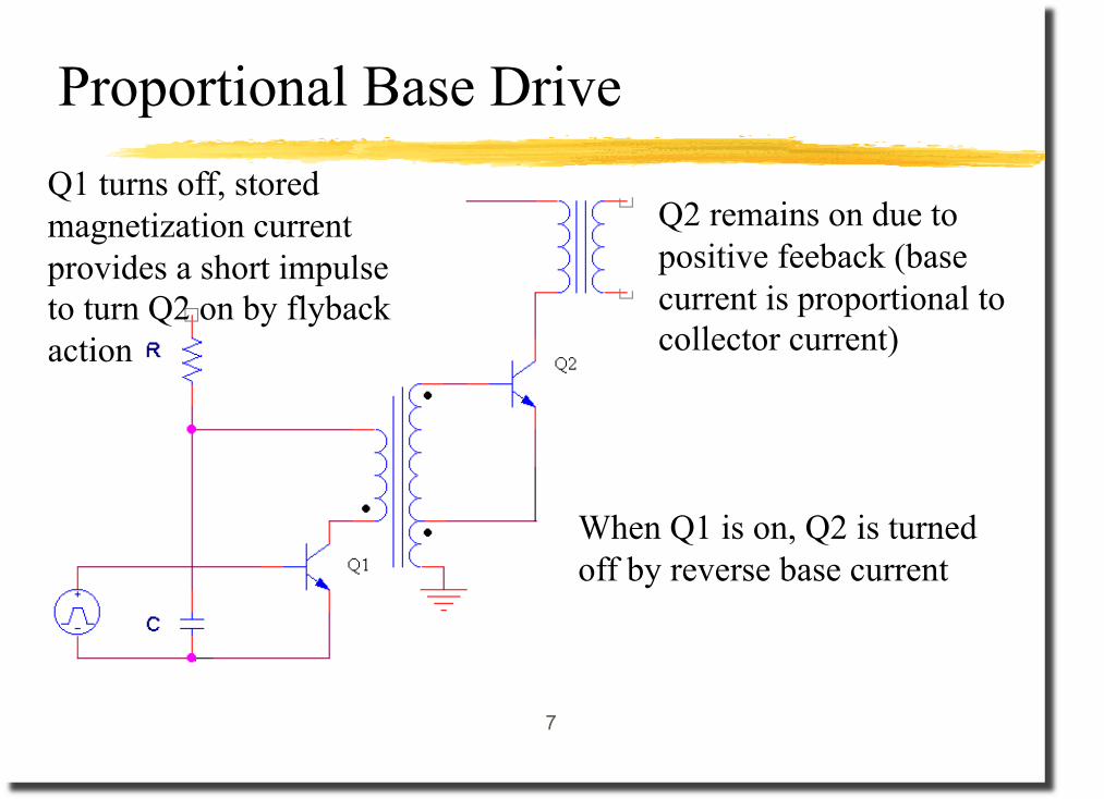
Proportional Base Drive Q1 turns off, stored magnetization current provides a short impulse to turn Q2 on by flyback action
Q2 remains on due to positive feeback (base current is proportional to collector current)
When Q1 is on, Q2 is turned off by reverse base current

8
Wood Base Drive
-ve voltage clamp
Reverse base current
Forward base current
Charged up during on time

9
Power MOSFETs
Voltage controlled devices No reverse recovery because using majority
carriers Drain current turnoff time is so fast that the
dissipation due to the overlap of falling current and rising voltage is generally negligible
Vds ON could be quite high, 2V to 3V, compared with Vce ON , 1 V, of bipolar

10
Required Gate Current
Voltage controlled device. Zero current? No, not a high speed switching!
178 V
150 pF
1800 pF 10 V gate pulse
I2
I1
For a rise time of 50 ns, I1 = 360 mA and I2 = 564 mA, i.e., required gate current is 0.924 A!!

11
Gate Rise and Fall Time for Desired Drain Current Rise and Fall Time
Say Vth = 2.5 V, Vg1 = 5 V for fully turn on of drain current
10 V gate pulse of 50 ns rise time, 10 V
Vgs
Ids Drain current rise time is only 12.5 ns!!
12
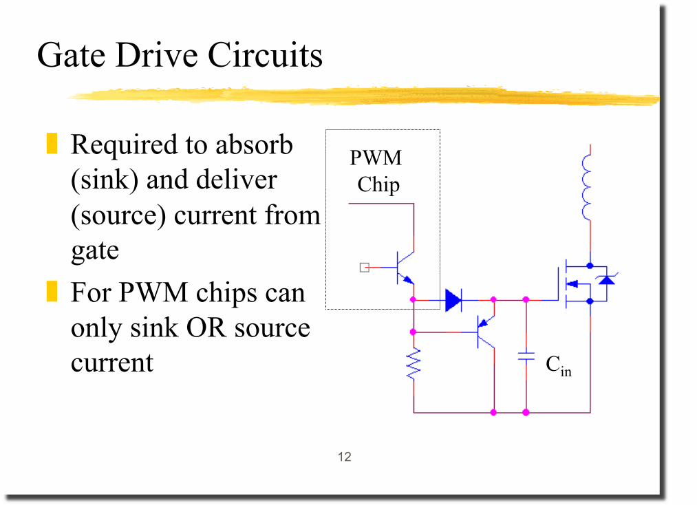
Gate Drive Circuits
Required to absorb (sink) and deliver (source) current from gate
For PWM chips can only sink OR source current Cin
PWM Chip

13
Gate Drive Circuits
Some PWM chips generate non-overlap gate pulse with totem pole outputs
B
A

14
Snubber Networks
Turn-Off Switching Losses Turn-Off Snubbers Non-Dissipative Snubbers

15
Turn-OFF Switching Losses
Bipolar power switches usually have slow turn-off time
Overlap of falling current and rising voltage accounts for most of the switching losses
Ic
Vce
Pd

16
Turn-OFF Switching Losses
Power MOSFET has shorter current fall time
But high -di/dt means higher voltage spike generation due to transformer leakage inductance
Id
Vds
Pd
Typical waveforms of a Forward converter

17
Turn-Off Snubbers
Snubber
C slows down the rise time Typical waveforms of a Forward
converter with snubber
Id
Vds
Pd

18
2Vdc
Ip
tf
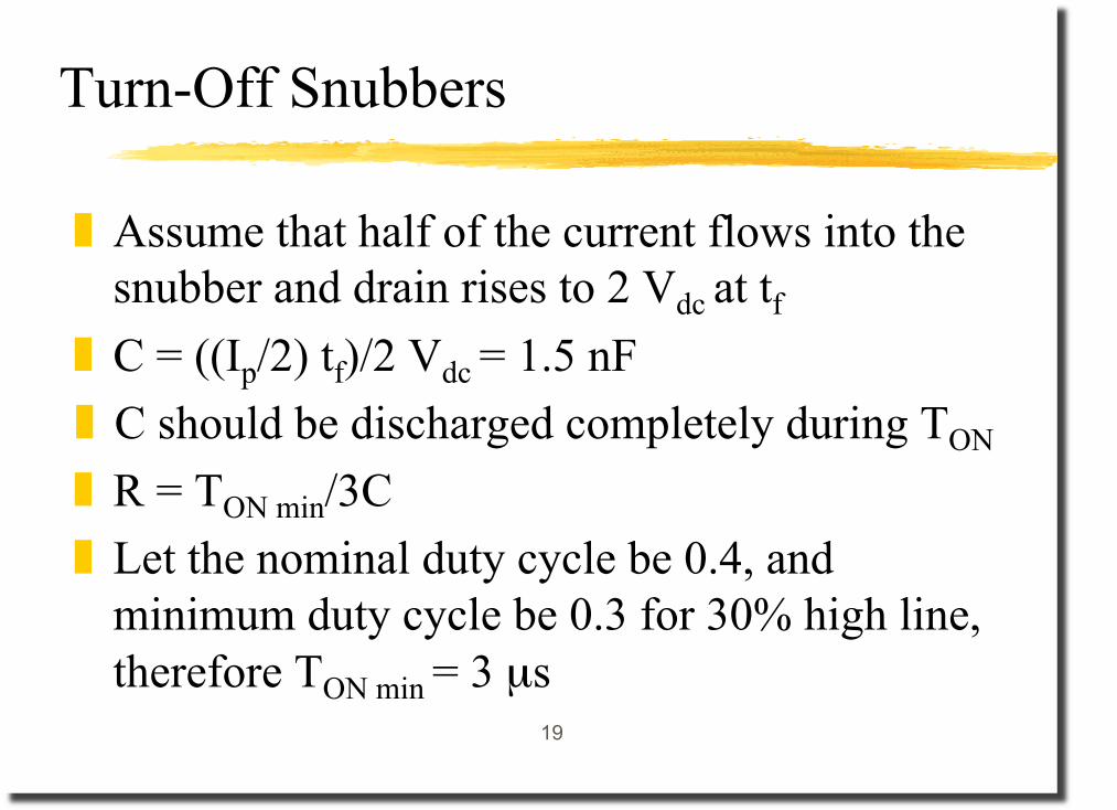
Turn-Off Snubbers
Vdc = 200 V, Ip = 4 A, tf = 0.3 µs, T = 10 µs Transistor dissipation without snubber PDQ = (2 × 200 × 4)/2 × 0.3/10 = 24 W
Drain voltage rises instantly with snubber
19
Turn-Off Snubbers
Assume that half of the current flows into the snubber and drain rises to 2 Vdc at tf
C = ((Ip/2) tf)/2 Vdc = 1.5 nF C should be discharged completely during TON
R = TON min/3C Let the nominal duty cycle be 0.4, and
minimum duty cycle be 0.3 for 30% high line, therefore TON min = 3 µs

20
Turn-Off Snubbers
R = 666 Ω The dissipation of snubber resistor is PDR = ½C(2 Vdc )2/T = 12 W
2Vdc
Ip/2
tf Drain voltage rises to
2Vdc in tf
with snubber
Half of the current flows to snubber capacitor

21
Turn-Off Snubbers
The dissipation of transistor with snubber can be estimated as
PDQ = ((Ip/2)(2 Vdc tf)/(6T) = 4 W
In practice, if the transistor is still too warm, increase C and have more dissipation on R.
Dissipation on R CANNOT be reduced by decreasing its value!!

22
Snubber Returned to Positive
Voltage stress on C becomes Vdc instead of 2 Vdc
For the same effect, double in value

23
Non-Dissipative Snubbers
Vdc

24
Protections
Inrush Limiting Start-Up Methods Soft Start Output Overvoltage Protection Current Limit Circuits Output Current Limiting

25
Inrush Limiting
Resistors for inrush current limiting
R = Vp/I
I is the half-cycle surge current ratings of
diodes

26
Inrush Limiting
For reducing dissipation, negative temperature coefficient thermistors (NTC) can be employed as inrush current limiting resistors
Protection may NOT work properly if SMPS is switch off and back on rapidly!
27
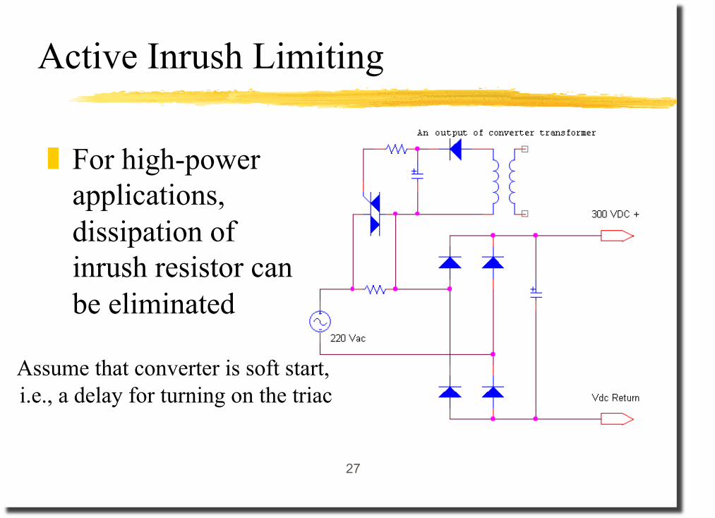
Active Inrush Limiting
For high-power applications, dissipation of inrush resistor can be eliminated
Assume that converter is soft start, i.e., a delay for turning on the triac

28
Dissipative (Passive) Start Circuit

29
Active Start Circuit
Transistor is off after start up

30
Impulse Start Circuit
Vz - VA < VD < Vz - Vstart
Vz
VD
VA

31
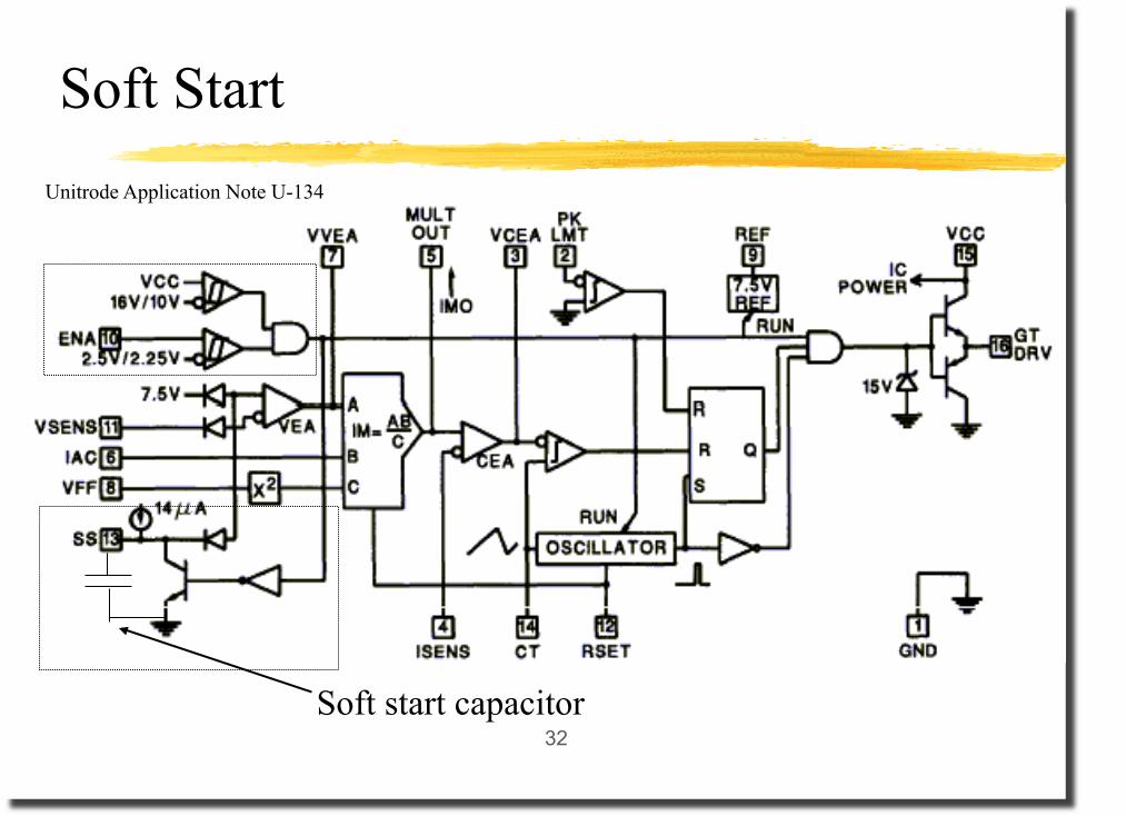
Soft Start
Resulting lower stress on converter components Progressively increase the duty cycle of the
PWM controller during start up Coupled with under voltage lock out in modern
controllers Start up should be slow enough to ensure that
there is no overshoot in the output during turn on
32
Soft Start Unitrode Application Note U-134
Soft start capacitor
33
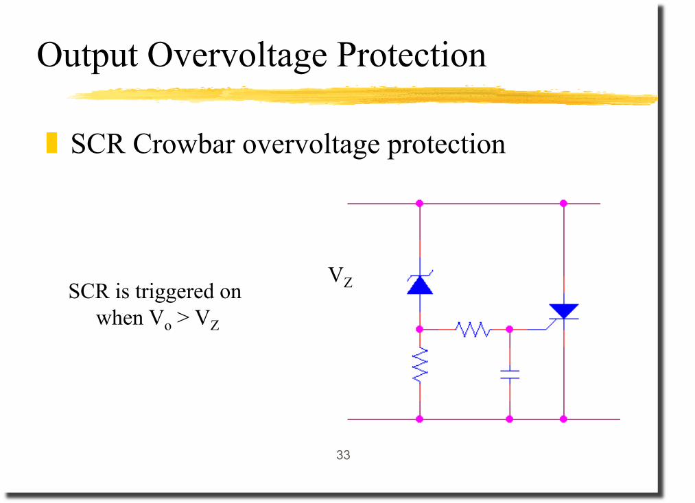
Output Overvoltage Protection
SCR Crowbar overvoltage protection
SCR is triggered on when Vo > VZ
VZ

34
Output Overvoltage Protection
SCR Crowbar with high precision

35
Current Limit Circuits
Pulse-by-pulse over-current limiting for primary-reference direct drive designs
PWM IC
Resetting the output
driver
Current sense resistor

36
Output Current Limiting
Non-dissipative current limit circuit for control on the output side
Vout Vin


![MOSFETs [CHAPTER 6]apachepersonal.miun.se/~gorthu/device/Omi.pdfmicrowave amplifiers •Higher input impedance than bipolar transistors •Thermally stable Negative temperature coefficient](https://static.fdocuments.net/doc/165x107/5e3a4e73b69ac32a5040b7b5/mosfets-chapter-6-gorthudeviceomipdf-microwave-amplifiers-ahigher-input-impedance.jpg)

