Scanning Tunneling Microscopy Local probes at high ... · Scanning Tunneling Microscopy Local...
37
www.uam.es/lbtuam Scanning Tunneling Microscopy Local probes at high magnetic fields ? Hermann Suderow Laboratorio de Bajas Temperaturas Departamento de Física de la Materia Condensada Instituto de Ciencia de Materiales Nicolás Cabrera Universidad Autónoma de Madrid (UAM)
Transcript of Scanning Tunneling Microscopy Local probes at high ... · Scanning Tunneling Microscopy Local...

ww
w.u
am.e
s/lb
tuam
Scanning Tunneling Microscopy
Local probes at high magnetic fields ?
Hermann Suderow
Laboratorio de Bajas Temperaturas
Departamento de Física de la Materia Condensada
Instituto de Ciencia de Materiales Nicolás Cabrera
Universidad Autónoma de Madrid (UAM)

Microscopyoptical
Always fascinating to obtain real space images
C. Zeiss, Jena
Antoni van Leeuwenhoek
(1632-1723) Delft
Franz Griendel von Ach

MicroscopyOptical, SEM, SPM
SPM at cryogenic temperatures
Cryogenic operation of a scanning probe microscope eliminates Brownian motion altogether, provides for resolution in energy and enables macroscopic
quantum behavior

Cryogenic scanning probe microscopy eliminates Brownian motion altogether and
enables macroscopic quantum behavior4
D. Eigler, IBM
Atomic scale manipulation with cryogenic scanning probe microscopy
T=4.2 K

Status of cryogenic scanning probe microscopy

What ?
Tunneling spectroscopy
Tunneling microscopy
Spectroscopy at high magnetic fields
pA

Piezoelectrics
V
Ayx 20, ≈∆
STM:Binnig and Rohrer (1982)
1Å ~ 250 mV
z
F eEVNzVIΦ−≈ 025.1)(),(
∆ I = 1 nA ~ ∆ z = 1Å

Tunneling current between a metallic tip and a sample:
Overlap between tip and sample’s wavefunctions. Bardeen’s formalism
( ) ( )( ) ( )
( )
( )∫
∑
∇−∇=
+
=
−+−=
−
**2
2
2
;
;
1
1)(
12
µµψψψψ
ψ
ψ
δπ
ννµν
νν
µµ
νµµννµν
µ
dSm
M
E
E
e
Ef
EEMeVEfEfe
I
Tk
EE
B
F
h
h
STM:
The tunneling current

Ideal tip, low bias voltage :
( ) ( ) ( )FF EEEI ,2
00dd ρδψ ν
νν =−∝∑
d0
STM: Contour map of the local density of states
STM:
The tunneling current

-4 -3 -2 -1 0 1 2 3 40
1
2
3
4∆=1mV
T=0.3 K
T=1 K
Bias voltage (eV/∆∆∆∆0)
Norm
aliz
ed tun
nelli
ng c
ondu
cta
nce
dEV
eVEfEN
dV
dI
∂
−∂∝ ∫
)()(
Low temperature spectroscopy
87 µeV = 1 K
22)(
∆−=
E
EEN
ϕψψ ie=
2
,
2
,,
)(kEkk
kk
rvv
rr
βα
βααβ
ε
ψψ
∆+=
∝∆−
),;( yxEN

Tunneling spectroscopy with STM:
vacuum Giaever tunneling
-1.2 -0.9 -0.6 -0.3 0.0 0.3 0.6 0.9 1.20.0
0.5
1.0
1.5
2.0
2.5T = 150 mK
200 G
∆ = 0.28 meV
Nor
mal
ized c
onduc
tanc
eBias voltage (mV)
The superconducting gap through local tunneling spectroscopy at very low
temperatures
Geneva, Cornell, Paris, Tokyo, …High Tc superconductors
-1 0 10.0
0.5
1.0
1.5
MgB2
norm
alize
d con
ductance
Normalized bias voltage
Two band superconductors
-4 -3 -2 -1 0 1 2 3 40.0
0.2
0.4
0.6
0.8
1.0
1.2
1.4
T = 0.15 K
Bias voltage (mV)
ErNi2B
2C
Tc=11K
Normalize
d conductance
-5 -4 -3 -2 -1 0 1 2 3 4 50.0
0.5
1.0
1.5
2.0
TmNi2B
2C
Tc = 10.5 K
Bias voltage (mV)
T = 0.8 K
Nor
mal
ized c
onduc
tanc
e
Magnetic superconductors
-2 - 1 0 1 20 .0
0 .5
1 .0
1 .5
2 .0
Tc= 1 .8 5 K
P rO s4S b
12
Normalized con
ductanc
e
B ia s vo lta ge / ∆0 ( = 1 .7 3 k
BT
c)
Sr2RuO4
BULK superconductingdensity of states
Averaged over part of the Fermi surface

- 3 - 2 - 1 0 1 2 30 .0
0 .5
1 .0
1 .5
2 .0
2 .5
Nor
mal
ized
con
duc
tanc
e
B ia s v o lt a g e (m V )-3 -2 -1 0 1 2 3
0.0
0.5
1.0
1.5
No
rmal
ized
co
nd
uct
ance
Bias voltage (mV)
2H-NbSe2
1.7nm
2H-NbS2
NbSe2 and NbS2 : two two-gap superconductors

1/λCDW
1/a
Charge order in 2H-NbSe2 at 100 mK
2H-NbSe2
2H-NbS2
0.2
9 n
m
1.2
5 n
m
0.35 nm
Se
Nba
b
c
( )%13 ±= aCDWλ1.7nm

-2.0 -1.5 -1.0 -0.5 0.0 0.5 1.0 1.5 2.00
1
2
3
4
5
No
rmal
ized
den
sity
of
Stat
es
Energy (meV)
-2.0 -1.5 -1.0 -0.5 0.0 0.5 1.0 1.50
1
2
3
4
5
No
rmal
ized
co
nd
uct
ance
Bias voltage (mV)
2H-NbS2 Electronic density of states vs. temperature
dEV
eVEfEN
dV
dIS
∂
−∂∝ ∫
)()( ( )ENS
Two gap superconductor NbS2

0 1 2 3 4 5 60.0
0.2
0.4
0.6
0.8
1.0
1.2 ∆
0=1.73 k
BT
c
∆ (
meV
)
Temperature (K)
2H-NbS2 Maxima of the gap distribution (two gap) vs. temperature
0.0 0.5 1.0 1.5 2.00.0
0.2
0.4
0.6
0.8
1.0
1.2
1.4
1.6
No
rmal
ized
den
sity
of
stat
es
Energy (meV)
Two gap superconductor NbS2

URu2Si2
Kondo systems
Strong coupling features
Andreev features
0 1 2 3 4 5 6 7 8 9 10 11 120.00
0.25
0.50
0.75
1.00
1.25
1.50
Q = 0.58
Q = 0.59
Q=0.57
Q = 0.55 - 0.56
H (
Te
sla
)
Temperatura (K)
Phase diagrams
Tunneling spectroscopy

What ?
Tunneling spectroscopy
Tunneling microscopy
Spectroscopy at high magnetic fields
pA

Piezoelectrics
V
Ayx 20, ≈∆
STM:Binnig and Rohrer (1982)
1Å ~ 250 mV
z
F eEVNzVIΦ−≈ 025.1)(),(
∆ I = 1 nA ~ ∆ z = 1Å

H
TTc
Hc1
Hc2
Hc
Meissner state
Mixed state
Normal phase
H
Meissner state
Mixed state
H
d
H(T)/50d(nm) ≈
r
s
2
nΨ ====
H
λξJ
J
Microscopy of the superconducting gap in type II materials
2
02
2πξ
φ=cH
ϕψψ ie=
βααβ ψψ,, kkrr
−∝∆ 22
)(∆−
=E
EEN

The vortex lattice through STM
Measure far below Tc (here 7 K)

0.6 nm
0 mV
0.4 µS
dI/dV
0.85 µS
21nm
0 µS
dI/dV
2.23 µS
-2 -1 0 1 20.0
0.4
0.8
1.2
1.6
2.0
2.4
Se atom
Hole
Co
nd
uct
ance
(µS
)
Bias voltage (mV)
0 mV
Atomic size tunneling spectroscopy inside vortices in 2H-NbSe2
T=100 mK

Local tunneling spectroscopy in the mixed state of superconductors
MgB2
Geneva, Paris, Argonne, Madrid
V3Si and Chevrel phasesMaryland, GenevaHigh Tc materials:
Geneva , Paris, Tokyo, Cornell , Princeton, …
Nickel borocarbidesTokyo, Argonne, Madrid
FeAsBeijing, Harvard, Tokyo …
NbSe2 and related compoundsBell labs, Paris, Madrid, Leiden

Temperature between (0.1K-2.1K)144 images
8 min each one
Several images at each T
Direct observation of thermally induced vortex depinning
Physics Today, see youtube channel physics updatehttp://www.youtube.com/watch?v=7fgNpqgZWKYhttp://www.youtube.com/user/citecnomik1

Spectroscopy at high magnetic fields
pA
How ?

Principles of design of STMs : From first large devices …
First cryogenic STM in Madrid
1988

100 mK + 10 T“Superinsulator”Vortex physicsNanostructures
10 mK + 9 TCurrent Drive STS
Heavy Fermions (Kondo lattice)
100 mK, 3D VECTOR MAGNETLayered materials
300 mK, 13 T -> 17 T Superconducting tips
100 mK
Facilities in Madrid
1. Spectroscopy
2. Macroscopic movement over the sample
3. Tip and sample preparation methods
STM/S in a dilution refrigerator• Compact design to guarantee mechanical stability (piezoelectric drive)• Home made electronics, cryogenics and mechanics
2 µm

V
nmyx 20, ≈∆
Principle of operation of a scanning tunneling microscope
Scanning window in the µm range with sub atomic
resolution
Fine positioning piezoelectrics +
XY
xyz
Z
Coarse motor
Position without
heating with nm resolution
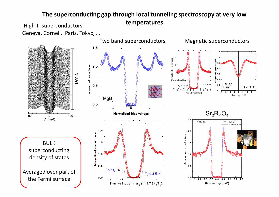
Stiffness
fmicroscope
fvibration isolation
effm
kf
π2
10 =
Designing a cryogenic scanning tunneling microscope
Soft and heavy
Stiff and light
Tip-sample motion shall be in phase

Mezclas de 3He y 4HeSTM holder for dilution refrigeration
� STM head is posed on fiber glass loom� Specific precision motion system using a series of ropes with a room temperature actuator without measurable heating at 100 mK

Mezclas de 3He y 4HeSTM electronics at LBTUAM
IndustrialPC
DACADC
Powersupply
+/- 15 V
+/- 140 V
OP276xPA243
Bias voltageRF filters
I-V converter
Tunnel current
RF
filters
Motor Z’Switchable
filter’
RF
filters
6 PIEZOSCANNING
DRIVES
… Power supply
+/- 15 V
Power supplyRF
filters
PA243
Resolution in spectroscopy of <15 µµµµeV (<150 mK)
RF filters

XY
xyz
Z
Spectroscopy at high magnetic fields
pA
X
Z
Compact system
Madrid: 17 Tsuperconducting magnet
Compact system
just for tunneling
maximally simplified
Microscope for high field superconducting solenoid

Web page of LBTUAMwww.uam.es/lbtuam

Workshop on high magnetic field science and technologyMiraflores de la Sierra, 6-9 November 2012
www.uam.es/inc
Organizers : H. Suderow and I. Guillamón

A. Maldonado, J.A. Galvis Echeverry, P. Kulkarni,A. Buendía,
I. Guillamón, J.G. Rodrigo, S. VieiraLaboratorio de Bajas Temperaturas
Dpto. Física de la Materia CondensadaInstituto de Ciencia de Materiales Nicolás Cabrera
Universidad Autónoma de Madrid (UAM)
J. Sesé, R. Córdoba, A. Fernández Pacheco, J.M. de Teresa, R. IbarraICMA, Unizar, Instituto de Nanociencia de Aragón
F. GuineaInstituto de Ciencia de Materiales de Madrid,
Consejo Superior de Investigaciones Científicas, Madrid
S. Bud’ko, P.C. CanfieldAmes Laboratory, Ames – USA
S. BannerjeeIIT Kanpur – India
T. Baturina, Novosibirsk, Russia, V. Vinokur, Argonne, USA
L. Cario, Nantes; P. Rodiere, P. Lejay, J.P. Brison, Dai Aoki, J. FlouquetInstitut Néel and SPSMS/DRFMC
E. Navarro Moratalla, C. Martí Gastaldo, E. Coronado, ICMol Valencia
V. Tissen, Chernogolovka, Russia
Scanning probe microscopy

The SEGAINVEX team (headed by M. Pazos)
www.lbtuam.es

Increasing the field in stepsNo time variation of flux distribution
Pinning produces spatial variation of BCritical state
FL=-FP
Vortex bundles with weak pinning at 100 mK
33 STS images0.04 T steps
0 1 2 3 40
1
2
3
4
5
6
Cam
po
Crí
tico
Hc2
(T
)
Temperatura (K)