Scanning tunneling microscopy studies of topological...
5
Scanning tunneling microscopy studies of topological insulators Peng Cheng a , Tong Zhang a,b , Ke He b , Xi Chen a , Xucun Ma b , Qikun Xue a,b,n a State Key Laboratory of Low-Dimensional Quantum Physics and Department of Physics, Tsinghua University, Beijing 100084, China b State Key Laboratory for Surface Physics, Institute of Physics, Chinese Academy of Sciences, Beijing 100190, China article info Article history: Received 20 September 2011 Accepted 5 November 2011 Available online 11 November 2011 abstract We summarize our recent scanning tunneling microscopy (STM) study of topological insulator thin films grown by molecular beam epitaxy (MBE), which includes the observation of electron standing waves on topological insulator surface and the Landau quantization of topological surface states. The work has provided valuable information to the understanding of intriguing properties of topological insulators, as predicted by theory. & 2011 Elsevier B.V. All rights reserved. 1. Introduction Topological insulator is a new class of quantum material, which possesses an energy gap in the bulk and nontrivial gapless states on the surface. The surface states are comprised of an odd number of massless Dirac cones in which crossing of two dispersion branches with opposite spins is fully protected by the time-reversal-symme- try at the Dirac point (Fig. 1). Topological insulators may provide new route to generating novel phases and quasi-particles, and may find applications in spintronics and quantum computing [1–7]. In 2009, a class of binary compounds [8–11], Bi 2 Se 3 , Bi 2 Te 3 and Sb 2 Te 3 , was shown to be the third generation of topological insulators. Compared to Bi 1 x Sb x (0.07 ox o0.22) alloy, the sur- face states of the Bi 2 Se 3 family contain only a single Dirac cone, making it easier to be studied. Also, these materials are stoichio- metric compounds and hence in principle can be prepared at higher purity and quality. Finally and perhaps most importantly for applications, Bi 2 Se 3 has a larger band gap of approximately 0.36 eV. It implies that topological behavior can sustain at room temperature. The unique properties of Bi 2 Se 3 family have been experimentally identified by, for example angle resolved photo- emission spectroscopy (ARPES), scanning tunneling microscopy (STM) and transport measurements. STM is a surface sensitive technique based on the concept of quantum tunneling. The atomically resolved structure of a surface can be obtained by monitoring the tunneling current in an STM. Besides its unprecedented capability to study surface topography, information on electronic structure at a given location of a sample can also be obtained. This type of measurement is called scanning tunneling spectroscopy (STS) and typically results in a plot of the local density of states (LDOS) as a function of energy of the sample. It has been widely used in the characterization of metals, semiconductors and superconductors. Applying it to the study of topological surface states, many intriguing properties have recently been unveiled. In this paper, we give an overview on the recent progress of STM study of topological insulators. 2. Electronic standing waves on topological insulators In a crystal, the electronic eigen-states are described by Bloch wavefunctions c k ðrÞ with energy e and wavevector k. The dispersion relation eðkÞ is usually measured by ARPES. In contrast, STM, which is a real space imaging technique, cannot be used to directly measure eðkÞ in momentum space. When disorders are introduced into a sample, the change in potential leads to the elastic electron scattering of the incident wave with a wave vector k i into k f ¼ k i þ q, with k i and k f being on the same constant-energy contour (CEC). The quantum interference between the initial and final states results in a standing wave pattern whose spatial period is given by l ¼ 2p=9q9, which are often referred to as the ‘‘Friedel oscillations’’. The phenomena can be observed by STM as modulations of the differential tunneling conductance. When the STM images of stand- ing waves are Fourier transformed, the scattering wave vector q becomes visible in the reciprocal space. This way, it simultaneously provides real-space and momentum-space information. In 1991, Don Eigler’s group and Avouris’ group independently reported the observation of standing waves on a metal surface by STM [12,13]. Afterwards, standing waves were imaged successively on other metal (Ag, Au and Be) and semiconductor surfaces, and even on high-T c superconductors and graphene. STM has become a powerful technique to study wavefunctions, electron scattering processes and dispersion relation of a material. The surface states of topological insulators possess spin-polarized Dirac-cone structure and are protected by time-reversal symmetry. Contents lists available at SciVerse ScienceDirect journal homepage: www.elsevier.com/locate/physe Physica E 1386-9477/$ - see front matter & 2011 Elsevier B.V. All rights reserved. doi:10.1016/j.physe.2011.11.004 n Corresponding author at: State Key Laboratory of Low-Dimensional Quantum Physics and Department of Physics, Tsinghua University, Beijing 100084, China. E-mail address: [email protected] (Q. Xue). Physica E 44 (2012) 912–916
Transcript of Scanning tunneling microscopy studies of topological...
Physica E 44 (2012) 912–916
Contents lists available at SciVerse ScienceDirect
Physica E
1386-94
doi:10.1
n Corr
Physics
E-m
journal homepage: www.elsevier.com/locate/physe
Scanning tunneling microscopy studies of topological insulators
Peng Cheng a, Tong Zhang a,b, Ke He b, Xi Chen a, Xucun Ma b, Qikun Xue a,b,n
a State Key Laboratory of Low-Dimensional Quantum Physics and Department of Physics, Tsinghua University, Beijing 100084, Chinab State Key Laboratory for Surface Physics, Institute of Physics, Chinese Academy of Sciences, Beijing 100190, China
a r t i c l e i n f o
Article history:
Received 20 September 2011
Accepted 5 November 2011Available online 11 November 2011
77/$ - see front matter & 2011 Elsevier B.V. A
016/j.physe.2011.11.004
esponding author at: State Key Laboratory o
and Department of Physics, Tsinghua Univer
ail address: [email protected] (Q. X
a b s t r a c t
We summarize our recent scanning tunneling microscopy (STM) study of topological insulator thin
films grown by molecular beam epitaxy (MBE), which includes the observation of electron standing
waves on topological insulator surface and the Landau quantization of topological surface states. The
work has provided valuable information to the understanding of intriguing properties of topological
insulators, as predicted by theory.
& 2011 Elsevier B.V. All rights reserved.
1. Introduction
Topological insulator is a new class of quantum material, whichpossesses an energy gap in the bulk and nontrivial gapless states onthe surface. The surface states are comprised of an odd number ofmassless Dirac cones in which crossing of two dispersion brancheswith opposite spins is fully protected by the time-reversal-symme-try at the Dirac point (Fig. 1). Topological insulators may providenew route to generating novel phases and quasi-particles, and mayfind applications in spintronics and quantum computing [1–7].
In 2009, a class of binary compounds [8–11], Bi2Se3, Bi2Te3 andSb2Te3, was shown to be the third generation of topologicalinsulators. Compared to Bi1�xSbx (0.07oxo0.22) alloy, the sur-face states of the Bi2Se3 family contain only a single Dirac cone,making it easier to be studied. Also, these materials are stoichio-metric compounds and hence in principle can be prepared athigher purity and quality. Finally and perhaps most importantlyfor applications, Bi2Se3 has a larger band gap of approximately0.36 eV. It implies that topological behavior can sustain at roomtemperature. The unique properties of Bi2Se3 family have beenexperimentally identified by, for example angle resolved photo-emission spectroscopy (ARPES), scanning tunneling microscopy(STM) and transport measurements.
STM is a surface sensitive technique based on the concept ofquantum tunneling. The atomically resolved structure of a surfacecan be obtained by monitoring the tunneling current in an STM.Besides its unprecedented capability to study surface topography,information on electronic structure at a given location of a samplecan also be obtained. This type of measurement is called scanningtunneling spectroscopy (STS) and typically results in a plot of the
ll rights reserved.
f Low-Dimensional Quantum
sity, Beijing 100084, China.
ue).
local density of states (LDOS) as a function of energy of thesample. It has been widely used in the characterization of metals,semiconductors and superconductors. Applying it to the study oftopological surface states, many intriguing properties haverecently been unveiled. In this paper, we give an overview onthe recent progress of STM study of topological insulators.
2. Electronic standing waves on topological insulators
In a crystal, the electronic eigen-states are described by Blochwavefunctions ckðrÞwith energy e and wavevector k. The dispersionrelation eðkÞ is usually measured by ARPES. In contrast, STM, whichis a real space imaging technique, cannot be used to directlymeasure eðkÞ in momentum space. When disorders are introducedinto a sample, the change in potential leads to the elastic electronscattering of the incident wave with a wave vector ki into kf¼kiþq,with ki and kf being on the same constant-energy contour (CEC). Thequantum interference between the initial and final states results in astanding wave pattern whose spatial period is given by l¼ 2p=9q9,which are often referred to as the ‘‘Friedel oscillations’’. Thephenomena can be observed by STM as modulations of thedifferential tunneling conductance. When the STM images of stand-ing waves are Fourier transformed, the scattering wave vector qbecomes visible in the reciprocal space. This way, it simultaneouslyprovides real-space and momentum-space information.
In 1991, Don Eigler’s group and Avouris’ group independentlyreported the observation of standing waves on a metal surface bySTM [12,13]. Afterwards, standing waves were imaged successivelyon other metal (Ag, Au and Be) and semiconductor surfaces, andeven on high-Tc superconductors and graphene. STM has become apowerful technique to study wavefunctions, electron scatteringprocesses and dispersion relation of a material.
The surface states of topological insulators possess spin-polarizedDirac-cone structure and are protected by time-reversal symmetry.
P. Cheng et al. / Physica E 44 (2012) 912–916 913
These unique characters are supposed to reflect in the scatteringprocesses and can be explored by standing waves using STM.
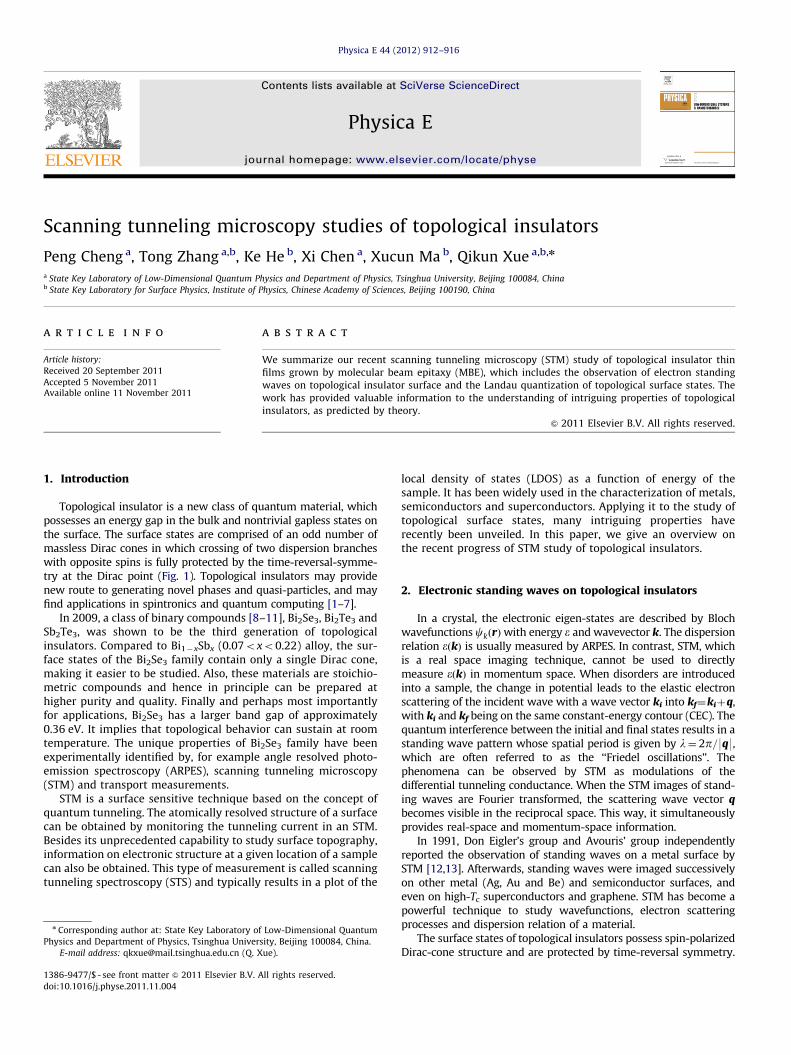
In this work, stoichiometric Bi2Te3 thin films were prepared onsingle crystal substrate Si(1 1 1) by MBE [14]. The atomically flatmorphology imaged by STM reveals high quality of our samples.The surface states of Bi2Te3 were investigated by STS, which givesa measure of the local density of states of electrons at energy eV.The differential conductance in the bulk insulating gap linearlydepends on the bias and is attributed to the gapless surface states.According to the calculations, the topological states of Bi2Te3 forma single Dirac cone at the center (G point) of the surface Brillouinzone (SBZ) and the surface states around the G point overlap inenergy with the bulk valence band. For this reason, the Diracpoint is invisible in STS.
We deposited a small amount of Ag atoms on the clean surfaceof the Bi2Te3 thin film. The atomically resolved STM image revealsthat a Ag atom substitutes a Bi atom in the second layer [15] ThedI/dV mapping was then carried out in a region containing Ag
Fig. 1. Single Dirac cone band structure of topological insulators.
Fig. 2. (a–f) Standing waves induced by Ag trimmers on Bi2Te3(1 1 1) surface at variou
current was set at 0.1 nA.
atoms. At each data point, the feedback was turned off and thebias modulation was turned onto record dI/dV. This procedureresults in a series of spatial mapping of LDOS at various biasvoltages.
Fig. 2(a–f) summarizes the dI/dV maps for bias voltagesranging from 50 to 400 mV. The first striking aspect of theseimages is the existence of standing waves in the vicinity of the Agatoms. This phenomenon strongly supports the surface nature oftopological states. For bulk states, there will be continuous rangesof wave vectors on the projected SBZ for a given energy. Usually,no distinct interference fringe can be produced by bulk states andvisualized by STM.
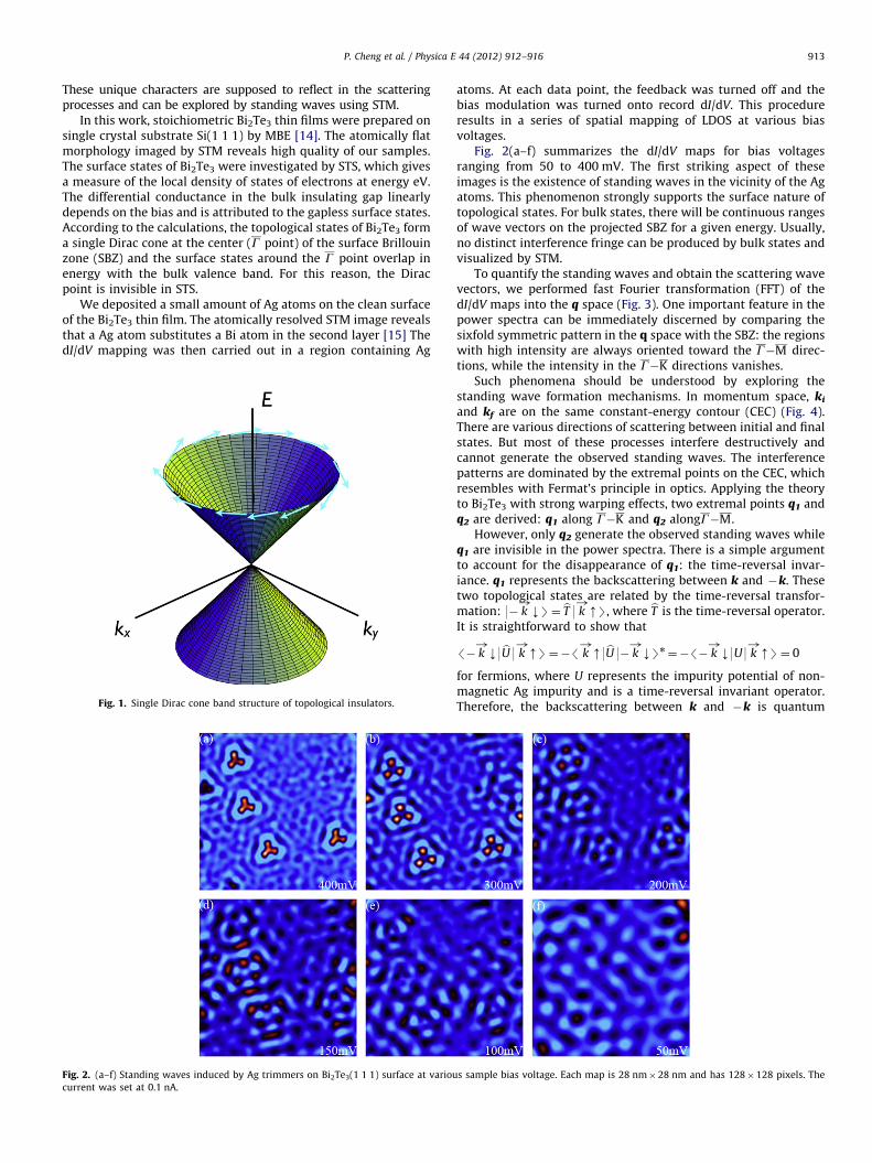
To quantify the standing waves and obtain the scattering wavevectors, we performed fast Fourier transformation (FFT) of thedI/dV maps into the q space (Fig. 3). One important feature in thepower spectra can be immediately discerned by comparing thesixfold symmetric pattern in the q space with the SBZ: the regionswith high intensity are always oriented toward the G�M direc-tions, while the intensity in the G�K directions vanishes.
Such phenomena should be understood by exploring thestanding wave formation mechanisms. In momentum space, ki
and kf are on the same constant-energy contour (CEC) (Fig. 4).There are various directions of scattering between initial and finalstates. But most of these processes interfere destructively andcannot generate the observed standing waves. The interferencepatterns are dominated by the extremal points on the CEC, whichresembles with Fermat’s principle in optics. Applying the theoryto Bi2Te3 with strong warping effects, two extremal points q1 andq2 are derived: q1 along G�K and q2 alongG�M.
However, only q2 generate the observed standing waves whileq1 are invisible in the power spectra. There is a simple argumentto account for the disappearance of q1: the time-reversal invar-iance. q1 represents the backscattering between k and �k. Thesetwo topological states are related by the time-reversal transfor-mation: 9� k
!kS¼ bT 9 k
!mS, where bT is the time-reversal operator.
It is straightforward to show that
/� k!
k9bU9 k!
mS¼�/ k!
m9bU9� k!
kSn¼�/� k
!k9U9 k!
mS¼ 0
for fermions, where U represents the impurity potential of non-magnetic Ag impurity and is a time-reversal invariant operator.Therefore, the backscattering between k and �k is quantum
s sample bias voltage. Each map is 28 nm�28 nm and has 128�128 pixels. The
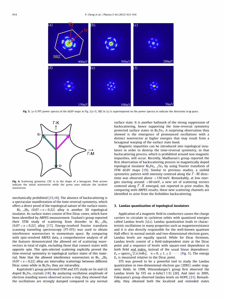
Fig. 3. (a–f) FFT power spectra of the dI/dV maps in Fig. 2(a–f). SBZ in (a) is superimposed on the power spectra to indicate the directions in q space.
Fig. 4. Scattering geometry. CEC is in the shape of a hexagram. Pink arrows
indicate the initial wavevector while the green ones indicate the incident
wavevector.
P. Cheng et al. / Physica E 44 (2012) 912–916914
mechanically prohibited [15,16]. The absence of backscattering isa spectacular manifestation of the time-reversal symmetry, whichoffers a direct proof of the topological nature of the surface states.
Bi1�xSbx (0.07oxo0.22) alloy is another 3D topologicalinsulator. Its surface states consist of five Dirac cones, which havebeen identified by ARPES measurement. Yazdani’s group reportedtheir STM study of scattering from disorder in Bi1�xSbx
(0.07oxo0.22) alloy [17]. Energy-resolved Fourier transformscanning tunneling spectroscopy (FT-STS) was used to obtaininterference wavevectors in momentum space. By comparingwith spin-resolved ARPES data, a comprehensive analysis of allthe features demonstrated the allowed set of scattering wave-vectors in total of eight, excluding those that connect states withopposite spin. This spin-selected scattering explicitly proved thetime-reversal symmetry in topological surface states of this mate-rial. Note that the allowed interference wavevectors in Bi1�xSbx
(0.07oxo0.22) alloy are intervalley scatterings between differentDirac cones while in Bi2Te3 they are intravalley.
Kapitulnik’s group performed STM and STS study on Sn and Cddoped Bi2Te3 crystals [18]. By analyzing oscillation amplitude ofelectron standing waves observed across a step, they showed thatthe oscillations are strongly damped compared to any normal
surface state. It is another hallmark of the strong suppression ofbackscattering, hence supporting the time-reversal symmetryprotected surface states in Bi2Te3. A surprising observation theyshowed is the emergence of pronounced oscillations with adistinct wavevector at higher energies that may result from ahexagonal warping of the surface state band.
Magnetic impurities can be introduced into topological insu-lators in order to destroy the time-reversal symmetry, so thatbackscattering process, which is prohibited around non-magneticimpurities, will occur. Recently, Madhavan’s group reported thefirst observation of backscattering process in magnetically dopedtopological insulator Bi2Fe2�xTe3 by using Fourier transform ofSTM dI/dV maps [19]. Similar to previous studies, a sixfoldsymmetric pattern with intensity centered along the G�M direc-tions was observed above þ150 meV. Remarkably, at low ener-gies starting around þ60 meV, a new set of scattering vectorscentered along G�K emerged, not reported in prior studies. Bycomparing with ARPES results, these new scattering channels areidentified to arise from the forbidden backscattering.
3. Landau quantization of topological insulators
Application of a magnetic field to conductors causes the chargecarriers to circulate in cyclotron orbits with quantized energiescalled Landau levels (LLs). Landau quantization leads to charac-teristic oscillations in many properties such as magnetoresistanceand it is also directly responsible for the well-known quantumHall effect. In normal metals and two-dimensional electron gases,Landau levels are equally spaced. While for Dirac fermions,Landau levels consist of a field-independent state at the Diracpoint and a sequence of levels with square-root dependence inboth field and index, instead of the usual linear dependence:En ¼ sgnðnÞ
ffiffiffiffiffiffiffiffiffiffiffiffiffiffiffiffiffiffiffiffiffiffi29n9_eBu2
F
q, n¼ 0,71,72UUUUUU (Fig. 5). The energy
En is measured relative to the Dirac point.STS was proved to be a powerful tool to study the Landau
quantization in two-dimensional electron gas (2DEG) under mag-netic fields. In 1998, Wiesendanger’s group first observed theLandau levels by STS on n-InAs(1 1 0) [20]. And later in 2005,Fukuyama’s group observed landau levels on HOPG [21]. Remark-ably, they obtained both the localized and extended states
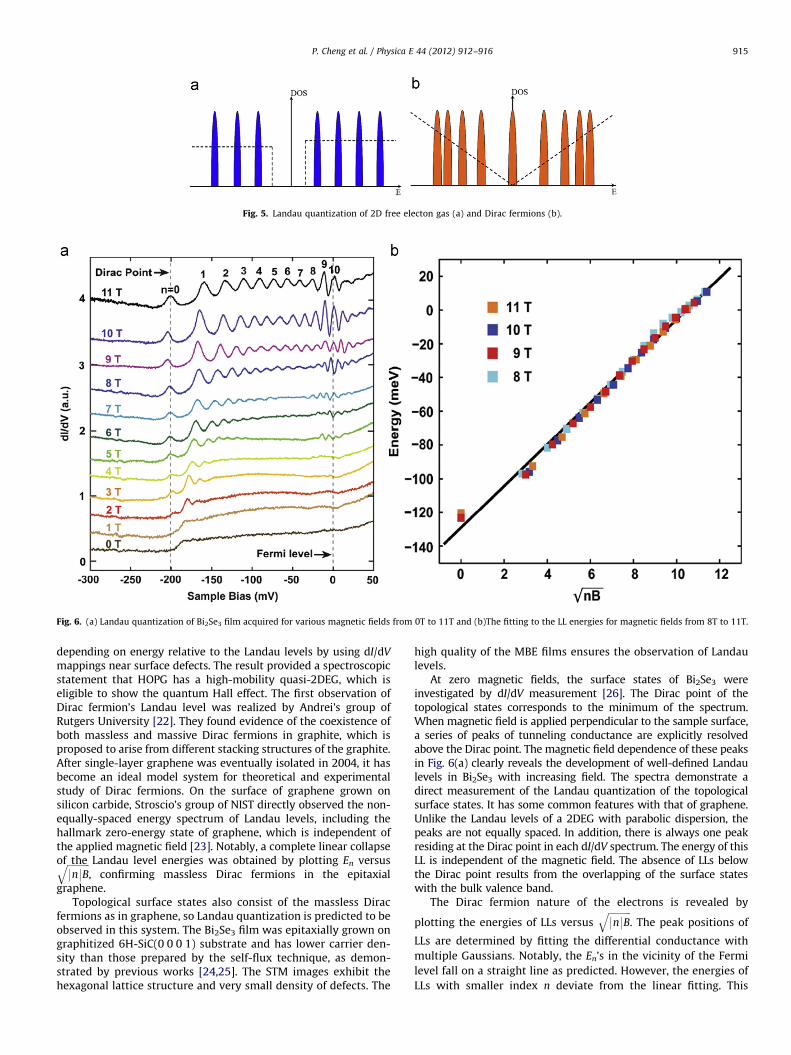
Fig. 5. Landau quantization of 2D free electon gas (a) and Dirac fermions (b).
Fig. 6. (a) Landau quantization of Bi2Se3 film acquired for various magnetic fields from 0T to 11T and (b)The fitting to the LL energies for magnetic fields from 8T to 11T.
P. Cheng et al. / Physica E 44 (2012) 912–916 915
depending on energy relative to the Landau levels by using dI/dV
mappings near surface defects. The result provided a spectroscopicstatement that HOPG has a high-mobility quasi-2DEG, which iseligible to show the quantum Hall effect. The first observation ofDirac fermion’s Landau level was realized by Andrei’s group ofRutgers University [22]. They found evidence of the coexistence ofboth massless and massive Dirac fermions in graphite, which isproposed to arise from different stacking structures of the graphite.After single-layer graphene was eventually isolated in 2004, it hasbecome an ideal model system for theoretical and experimentalstudy of Dirac fermions. On the surface of graphene grown onsilicon carbide, Stroscio’s group of NIST directly observed the non-equally-spaced energy spectrum of Landau levels, including thehallmark zero-energy state of graphene, which is independent ofthe applied magnetic field [23]. Notably, a complete linear collapseof the Landau level energies was obtained by plotting En versusffiffiffiffiffiffiffiffiffiffi9n9B
q, confirming massless Dirac fermions in the epitaxial
graphene.Topological surface states also consist of the massless Dirac
fermions as in graphene, so Landau quantization is predicted to beobserved in this system. The Bi2Se3 film was epitaxially grown ongraphitized 6H-SiC(0 0 0 1) substrate and has lower carrier den-sity than those prepared by the self-flux technique, as demon-strated by previous works [24,25]. The STM images exhibit thehexagonal lattice structure and very small density of defects. The
high quality of the MBE films ensures the observation of Landaulevels.
At zero magnetic fields, the surface states of Bi2Se3 wereinvestigated by dI/dV measurement [26]. The Dirac point of thetopological states corresponds to the minimum of the spectrum.When magnetic field is applied perpendicular to the sample surface,a series of peaks of tunneling conductance are explicitly resolvedabove the Dirac point. The magnetic field dependence of these peaksin Fig. 6(a) clearly reveals the development of well-defined Landaulevels in Bi2Se3 with increasing field. The spectra demonstrate adirect measurement of the Landau quantization of the topologicalsurface states. It has some common features with that of graphene.Unlike the Landau levels of a 2DEG with parabolic dispersion, thepeaks are not equally spaced. In addition, there is always one peakresiding at the Dirac point in each dI/dV spectrum. The energy of thisLL is independent of the magnetic field. The absence of LLs belowthe Dirac point results from the overlapping of the surface stateswith the bulk valence band.
The Dirac fermion nature of the electrons is revealed by
plotting the energies of LLs versusffiffiffiffiffiffiffiffiffiffi9n9B
q. The peak positions of
LLs are determined by fitting the differential conductance with
multiple Gaussians. Notably, the En’s in the vicinity of the Fermi
level fall on a straight line as predicted. However, the energies of
LLs with smaller index n deviate from the linear fitting. This
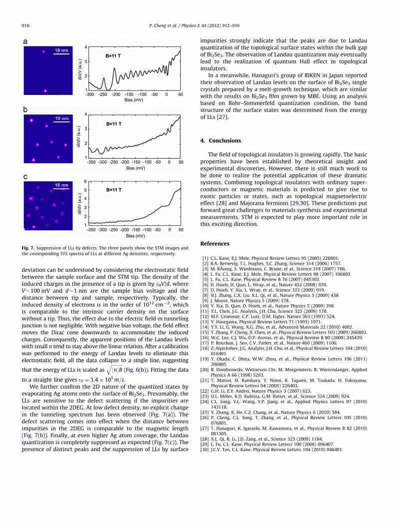
Fig. 7. Suppression of LLs by defects. The three panels show the STM images and
the corresponding STS spectra of LLs at different Ag densities, respectively.
P. Cheng et al. / Physica E 44 (2012) 912–916916
deviation can be understood by considering the electrostatic fieldbetween the sample surface and the STM tip. The density of theinduced charges in the presence of a tip is given by e0V/d, whereV�100 mV and d�1 nm are the sample bias voltage and thedistance between tip and sample, respectively. Typically, theinduced density of electrons is in the order of 1012 cm�2, whichis comparable to the intrinsic carrier density on the surfacewithout a tip. Thus, the effect due to the electric field in tunnelingjunction is not negligible. With negative bias voltage, the field effectmoves the Dirac cone downwards to accommodate the inducedcharges. Consequently, the apparent positions of the Landau levelswith small n tend to stay above the linear relation. After a calibrationwas performed to the energy of Landau levels to eliminate thiselectrostatic field, all the data collapse to a single line, suggesting
that the energy of LLs is scaled asffiffiffiffiffiffiffiffiffiffi9n9B
q(Fig. 6(b)). Fitting the data
to a straight line gives uF ¼ 3:4� 105 m=s.We further confirm the 2D nature of the quantized states by
evaporating Ag atoms onto the surface of Bi2Se3. Presumably, theLLs are sensitive to the defect scattering if the impurities arelocated within the 2DEG. At low defect density, no explicit changein the tunneling spectrum has been observed (Fig. 7(a)). Thedefect scattering comes into effect when the distance betweenimpurities in the 2DEG is comparable to the magnetic length(Fig. 7(b)). Finally, at even higher Ag atom coverage, the Landauquantization is completely suppressed as expected (Fig. 7(c)). Thepresence of distinct peaks and the suppression of LLs by surface
impurities strongly indicate that the peaks are due to Landauquantization of the topological surface states within the bulk gapof Bi2Se3. The observation of Landau quantization may eventuallylead to the realization of quantum Hall effect in topologicalinsulators.
In a meanwhile, Hanaguri’s group of RIKEN in Japan reportedtheir observation of Landau levels on the surface of Bi2Se3 singlecrystals prepared by a melt-growth technique, which are similarwith the results on Bi2Se3 film grown by MBE. Using an analysisbased on Bohr–Sommerfeld quantization condition, the bandstructure of the surface states was determined from the energyof LLs [27].
4. Conclusions
The field of topological insulators is growing rapidly. The basicproperties have been established by theoretical insight andexperimental discoveries. However, there is still much work tobe done to realize the potential application of these dramaticsystems. Combining topological insulators with ordinary super-conductors or magnetic materials is predicted to give rise toexotic particles or states, such as topological magnetoelectriceffect [28] and Majorana fermions [29,30]. These predictions putforward great challenges to materials synthesis and experimentalmeasurements. STM is expected to play more important role inthis exciting direction.
References
[1] C.L. Kane, E.J. Mele, Physical Review Letters 95 (2005) 226801.[2] B.A. Bernevig, T.L. Hughes, S.C. Zhang, Science 314 (2006) 1757.[3] M. KAonig, S. Wiedmann, C. Brune, et al., Science 318 (2007) 766.[4] L. Fu, C.L. Kane, E.J. Mele, Physical Review Letters 98 (2007) 106803.[5] L. Fu, C.L. Kane, Physical Review B 76 (2007) 045302.[6] D. Hsieh, D. Qian, L. Wray, et al., Nature 452 (2008) 970.[7] D. Hsieh, Y. Xia, L. Wray, et al., Science 323 (2009) 919.[8] H.J. Zhang, C.X. Liu, X.L. Qi, et al., Nature Physics 5 (2009) 438.[9] J. Moore, Nature Physics 5 (2009) 378.
[10] Y. Xia, D. Qian, D. Hsieh, et al., Nature Physics 5 (2009) 398.[11] Y.L. Chen, J.G. Analytis, J.H. Chu, Science 325 (2009) 178.[12] M.F. Crommie, C.P. Lutz, D.M. Eigler, Nature 363 (1993) 524.[13] Y. Hasegawa, Physical Review Letters 71 (1993) 1071.[14] Y.Y. Li, G. Wang, X.G. Zhu, et al., Advanced Materials 22 (2010) 4002.[15] T. Zhang, P. Cheng, X. Chen, et al., Physical Review Letters 103 (2009) 266803.[16] W.C. Lee, C.J. Wu, D.P. Arovas, et al., Physical Review B 80 (2009) 245439.[17] P. Roushan, J. Seo, C.V. Parker, et al., Nature 460 (2009) 1106.[18] Z. Alpichshev, J.G. Analytis, J.H. Chu, et al., Physical Review Letters 104 (2010)
016401.[19] Y. Okada, C. Dhita, W.W. Zhou, et al., Physical Review Letters 106 (2011)
206805.[20] R. Dombrowski, Wittneven Chr, M. Morgenstern, R. Wiesendanger, Applied
Physics A 66 (1998) S203.[21] T. Matsui, H. Kambara, Y. Niimi, K. Tagami, M. Tsukada, H. Fukuyama,
Physical Review Letters 94 (2005) 226403.[22] G.H. Li, E.Y. Andrei, Nature Physics 3 (2007) 623.[23] D.L. Miller, K.D. Kubista, G.M. Rutter, et al., Science 324 (2009) 924.[24] C.L. Song, Y.L. Wang, Y.P. Jiang, et al., Applied Physics Letters 97 (2010)
143118.[25] Y. Zhang, K. He, C.Z. Chang, et al., Nature Physics 6 (2010) 584.[26] P. Cheng, C.L. Song, T. Zhang, et al., Physical Review Letters 105 (2010)
076801.[27] T. Hanaguri, K. Igarashi, M. Kawamura, et al., Physical Review B 82 (2010)
081305.[28] X.L. Qi, R. Li, J.D. Zang, et al., Science 323 (2009) 1184.[29] L. Fu, C.L. Kane, Physical Review Letters 100 (2008) 096407.[30] J.C.Y. Teo, C.L. Kane, Physical Review Letters 104 (2010) 046401.