Roll-to-Roll deppgosition for Organic Light Emitting …...IMAGES ROLL TO ROLL VACUUM COATER winding...
25
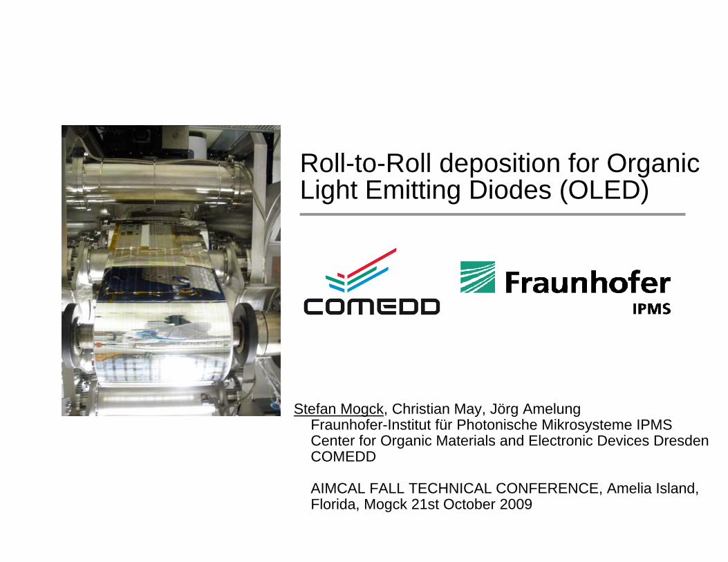
Roll-to-Roll deposition for Organic Light Emitting Diodes (OLED) Stefan Mogck , Christian May, Jörg Amelung Fraunhofer-Institut für Photonische Mikrosysteme IPMS Center for Organic Materials and Electronic Devices Dresden COMEDD COMEDD AIMCAL FALL TECHNICAL CONFERENCE, Amelia Island, Florida, Mogck 21st October 2009
Transcript of Roll-to-Roll deppgosition for Organic Light Emitting …...IMAGES ROLL TO ROLL VACUUM COATER winding...
Roll-to-Roll deposition for Organic p gLight Emitting Diodes (OLED)
Stefan Mogck, Christian May, Jörg AmelungFraunhofer-Institut für Photonische Mikrosysteme IPMSCenter for Organic Materials and Electronic Devices Dresden COMEDDCOMEDD
AIMCAL FALL TECHNICAL CONFERENCE, Amelia Island, Florida, Mogck 21st October 2009
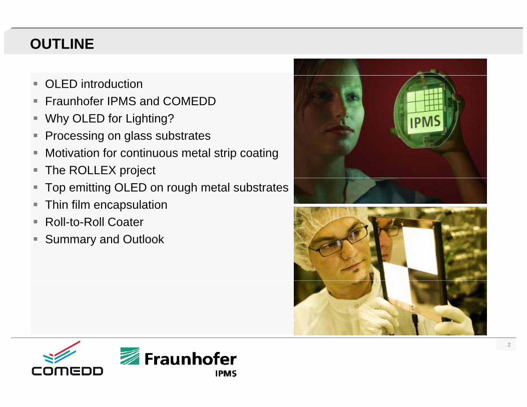
OUTLINE
OLED introductionFraunhofer IPMS and COMEDDWhy OLED for Lighting?Processing on glass substrates Motivation for continuous metal strip coatingThe ROLLEX projectTop emitting OLED on rough metal substratesThin film encapsulationRoll-to-Roll CoaterSummary and Outlook
2
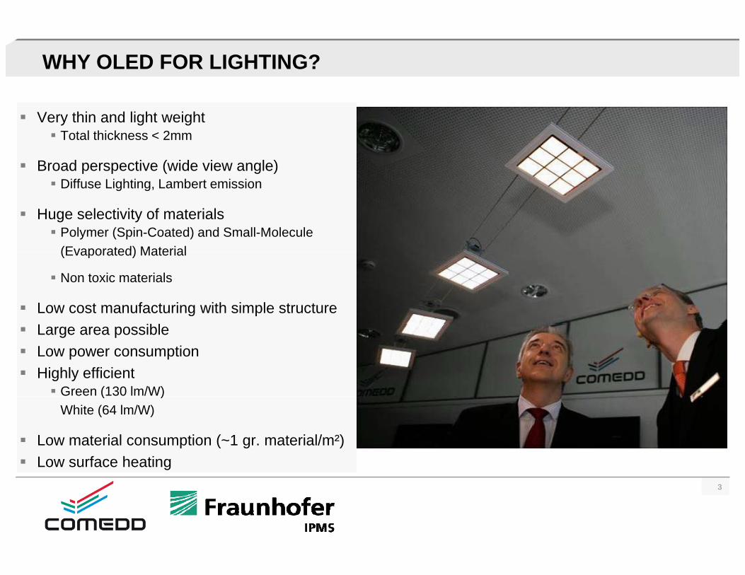
WHY OLED FOR LIGHTING?
Very thin and light weightTotal thickness < 2mm
Broad perspective (wide view angle)Diff Li h i L b i iDiffuse Lighting, Lambert emission
Huge selectivity of materialsPolymer (Spin-Coated) and Small-Molecule (Evaporated) Material(Evaporated) Material
Non toxic materials
Low cost manufacturing with simple structureL iblLarge area possibleLow power consumptionHighly efficient
Green (130 lm/W)( )White (64 lm/W)
Low material consumption (~1 gr. material/m²)Low surface heating
3
g
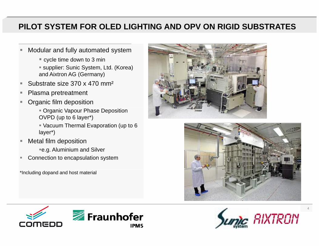
PILOT SYSTEM FOR OLED LIGHTING AND OPV ON RIGID SUBSTRATES
Modular and fully automated systemcycle time down to 3 minsupplier: Sunic System, Ltd. (Korea)
and Aixtron AG (Germany)( y)
Substrate size 370 x 470 mm²Plasma pretreatmentOrganic film deposition
Organic Vapour Phase Deposition OVPD (up to 6 layer*)
Vacuum Thermal Evaporation (up to 6 layer*)
fMetal film depositione.g. Aluminium and Silver
Connection to encapsulation system
*Including dopand and host material
4
5
MOTIVATION
Roadmap of the US Display Consortium forOLED-lighting
Absolutely not possible to reach by usingOLED display materials and techniquesp y q
New technologies for high efficient andsimultaneously low-priced OLEDs neededto meet special requirements of general lightingto meet special requirements of general lighting market:
Roll-to-roll-concept: noticeable lower coating costs in comparison to cluster or inline concepts
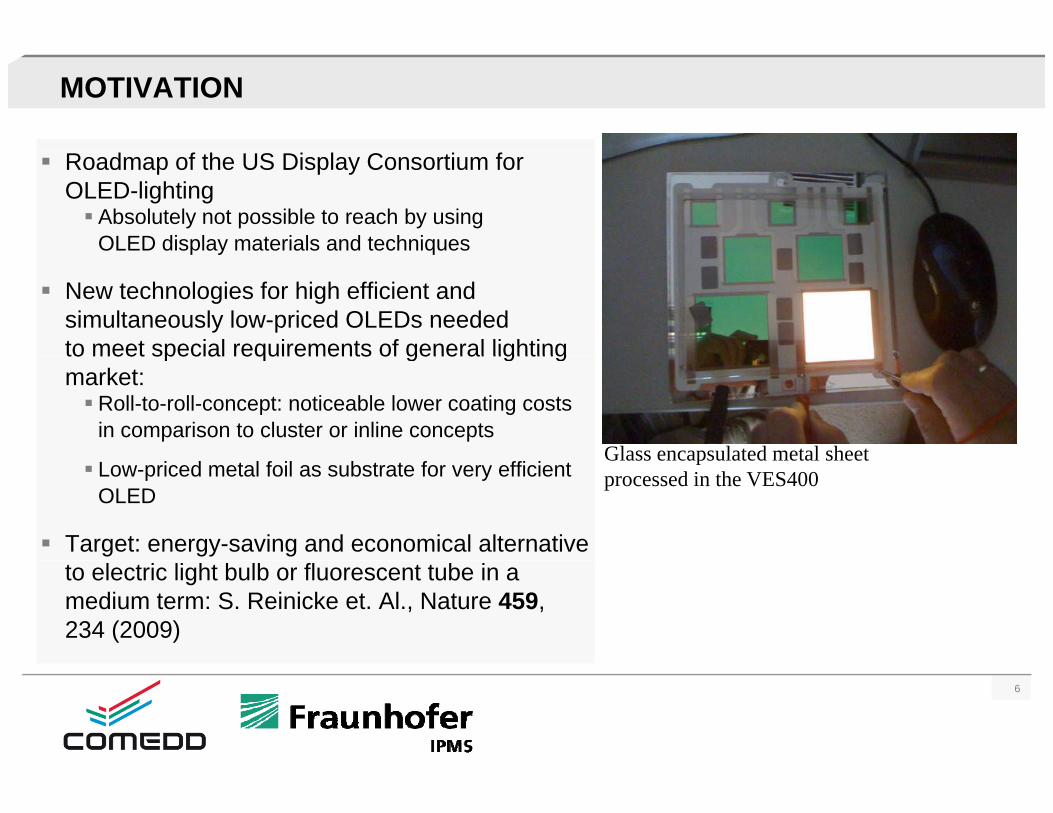
Glass encapsulated metal sheetLow-priced metal foil as substrate for very efficient OLED
Target: energy-saving and economical alternative
Glass encapsulated metal sheet processed in the VES400
to electric light bulb or fluorescent tube in a medium term: S. Reinicke et. Al., Nature 459, 234 (2009)
6
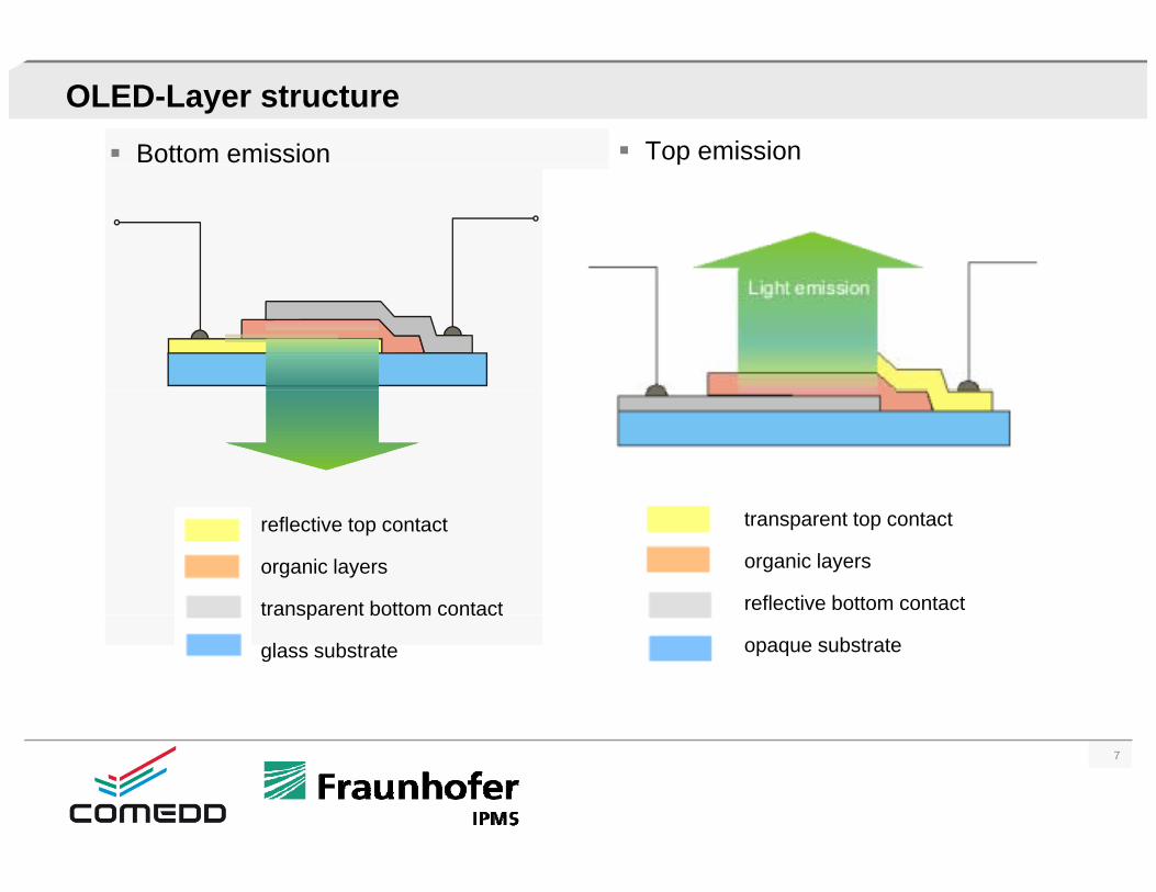
Bottom emission Top emission
OLED-Layer structure
transparent top contact
organic layers
reflective bottom contact
reflective top contact
organic layers
transparent bottom contact
opaque substrate
transparent bottom contact
glass substrate
7
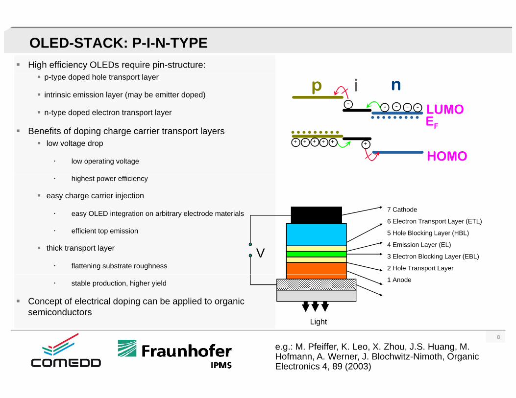
OLED-STACK: P-I-N-TYPEHigh efficiency OLEDs require pin-structure:
p-type doped hole transport layer
intrinsic emission layer (may be emitter doped)
n-type doped electron transport layer LUMO
p i n
EF
-----
Benefits of doping charge carrier transport layerslow voltage drop
low operating voltage HOMO
EF
+ + + + + +
highest power efficiency
easy charge carrier injection
easy OLED integration on arbitrary electrode materials 7 Cathode
6 Electron Transport Layer (ETL)efficient top emission
thick transport layer
flattening substrate roughness
p y ( )
5 Hole Blocking Layer (HBL)
4 Emission Layer (EL)
3 Electron Blocking Layer (EBL)
2 Hole Transport Layer
V
stable production, higher yield
Concept of electrical doping can be applied to organic semiconductors
1 Anode
Light
8
g
e.g.: M. Pfeiffer, K. Leo, X. Zhou, J.S. Huang, M. Hofmann, A. Werner, J. Blochwitz-Nimoth, Organic Electronics 4, 89 (2003)
TYPICAL DEFECTS ON BARE METAL SUBSTRATE
Defects and scratches on Al foil
S b t t RMS (R ) M h (R ) R h
Visible texture from the fabrication process
Cleaned and Ag coated Al sheet
Substrate RMS (Ra) Mean roughness (Ra) Roughness peak
Al foil with non-conductive smoothing dielectrical
surface
1.6 nm 1.3 nm 31.1 nmTypically OLED are deposited on very smooth ITO substrates
RMS 1Al foil with evaporated Ag at IPMS
2.5 nm 2.0 nm 24.9 nm
Glass substrate evaporated with Ag at
2.7 nm 2.1 nm 21.6 nm
RMS < 1 nm, spikes < 10 nm
9
gIPMS
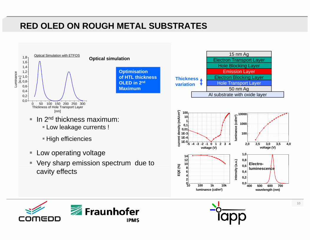
RED OLED ON ROUGH METAL SUBSTRATES
15 nm AgElectron Transport Layer
Hole Blocking LayerEmission LayerOptimisation1,2
1,41,61,8
ce
Optical Simulation with ETFOSOptical simulation
Electron Blocking LayerHole Transport Layer
50 nm AgAl substrate with oxide layer
of HTL thicknessOLED in 2nd
Maximum
0 50 100 150 200 250 3000,00,20,40,60,81,0
Lum
inan
[a.u
.] Thicknessvariation
1E-30,010,1
110
100
dens
ity (m
A/cm
²)
inan
ce (c
d/m
²)
100
1000
10000
In 2nd thickness maximum:Low leakage currents !
Thickness of Hole Transport Layer[nm]
0 6
0,8
1,0
-5 -4 -3 -2 -1 0 1 2 3 41E-51E-4
a.u.
)
%)
voltage (V)voltage (V)curr
ent
lum
i
2,0 2,5 3,0 3,5 4,0
101214
High efficiencies
Low operating voltageVery sharp emission spectrum due to Electro-
400 500 600 7000,0
0,2
0,4
0,6
wavelength (nm)
inte
nsity
(
luminance (cd/m²)
EQE
(%
10 100 1k 10k02468
y p pcavity effects luminescence
10
Non-conducting passivation laye
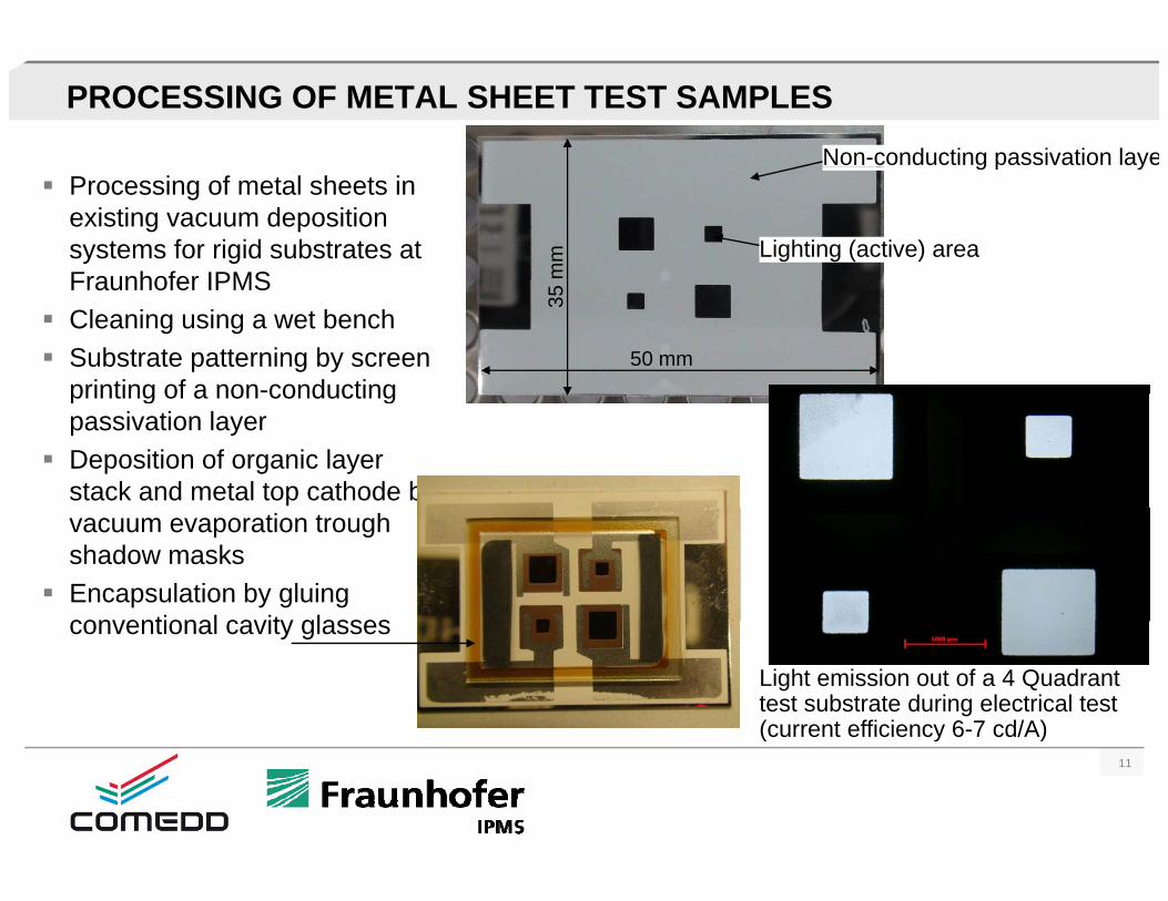
PROCESSING OF METAL SHEET TEST SAMPLES
Processing of metal sheets in existing vacuum deposition systems for rigid substrates at Fraunhofer IPMS
Lighting (active) area
g p y
mm
Fraunhofer IPMSCleaning using a wet benchSubstrate patterning by screen printing of a non-conducting
35
50 mmprinting of a non conducting passivation layerDeposition of organic layer stack and metal top cathode by vacuum evaporation trough shadow masksEncapsulation by gluing conventional cavity glassesconventional cavity glasses
Light emission out of a 4 Quadrant test substrate during electrical test (current efficiency 6-7 cd/A)
11
(current efficiency 6 7 cd/A)
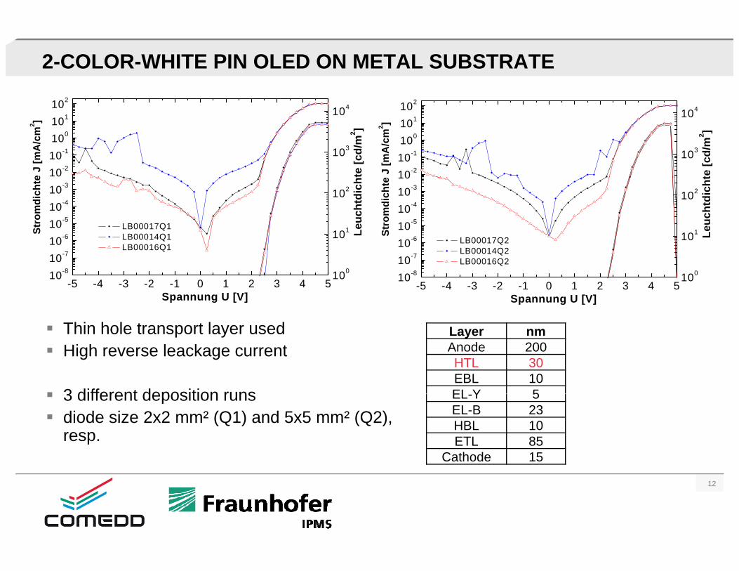
2-COLOR-WHITE PIN OLED ON METAL SUBSTRATE
1024 102
10-2
10-1
100
101
10
103
104
e J
[mA
/cm
2 ]
te [c
d/m
2 ]
10-2
10-1
100
101
10
103
104
e J
[mA
/cm
2 ]
te [c
d/m
2 ]
10-6
10-5
10-4
10-3
101
102
Stro
mdi
chte
LB00017Q1 LB00014Q1LB00016Q1
Leuc
htdi
ch
10-6
10-5
10-4
10-3
10
101
102
LB00017Q2LB00014Q2
Stro
mdi
chte
Leuc
htdi
cht
-5 -4 -3 -2 -1 0 1 2 3 4 510-8
10-7
100
Spannung U [V]
LB00016Q1
-5 -4 -3 -2 -1 0 1 2 3 4 510-8
10-7
100
LB00014Q2 LB00016Q2
Spannung U [V]
Layer nmAnode 200HTL 30EBL 10EL Y 5
Thin hole transport layer usedHigh reverse leackage current
3 different deposition runs EL-Y 5EL-B 23HBL 10ETL 85
Cathode 15
3 different deposition runsdiode size 2x2 mm² (Q1) and 5x5 mm² (Q2), resp.
12
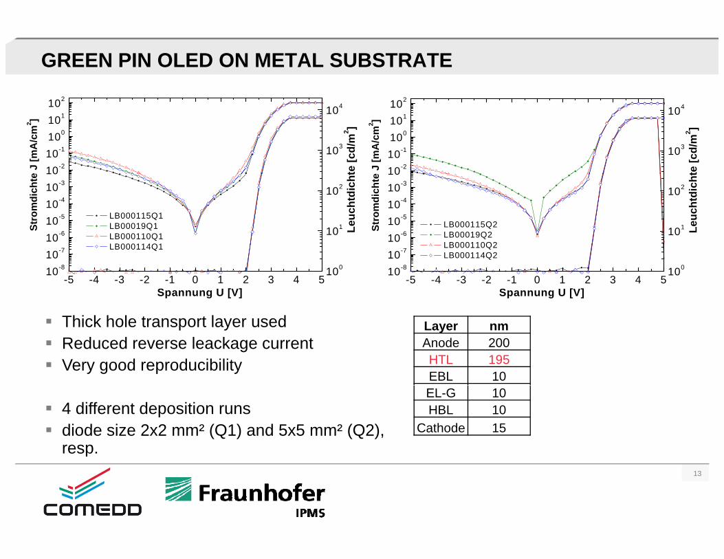
GREEN PIN OLED ON METAL SUBSTRATE
1021024
10-2
10-1
100
101
10
103
104
e J
[mA
/cm
2 ]
te [c
d/m
2 ]
10-2
10-1
100
101
10
103
104
e J
[mA
/cm
2 ]
te [c
d/m
2 ]
10-6
10-5
10-4
10-3
10
101
102
LB000115Q2 LB00019Q2LB000110Q2
Stro
mdi
chte
Leuc
htdi
cht
10-6
10-5
10-4
10-3
10
101
102
Stro
mdi
chte
LB000115Q1 LB00019Q1 LB000110Q1LB000114Q1
Leuc
htdi
cht
-5 -4 -3 -2 -1 0 1 2 3 4 510-8
10-7
100
LB000110Q2 LB000114Q2
Spannung U [V]-5 -4 -3 -2 -1 0 1 2 3 4 5
10-8
10-7
100
Spannung U [V]
LB000114Q1
Layer nmAnode 200HTL 195EBL 10
Thick hole transport layer usedReduced reverse leackage currentVery good reproducibility
EL-G 10HBL 10
Cathode 154 different deposition runsdiode size 2x2 mm² (Q1) and 5x5 mm² (Q2), resp.
13
p
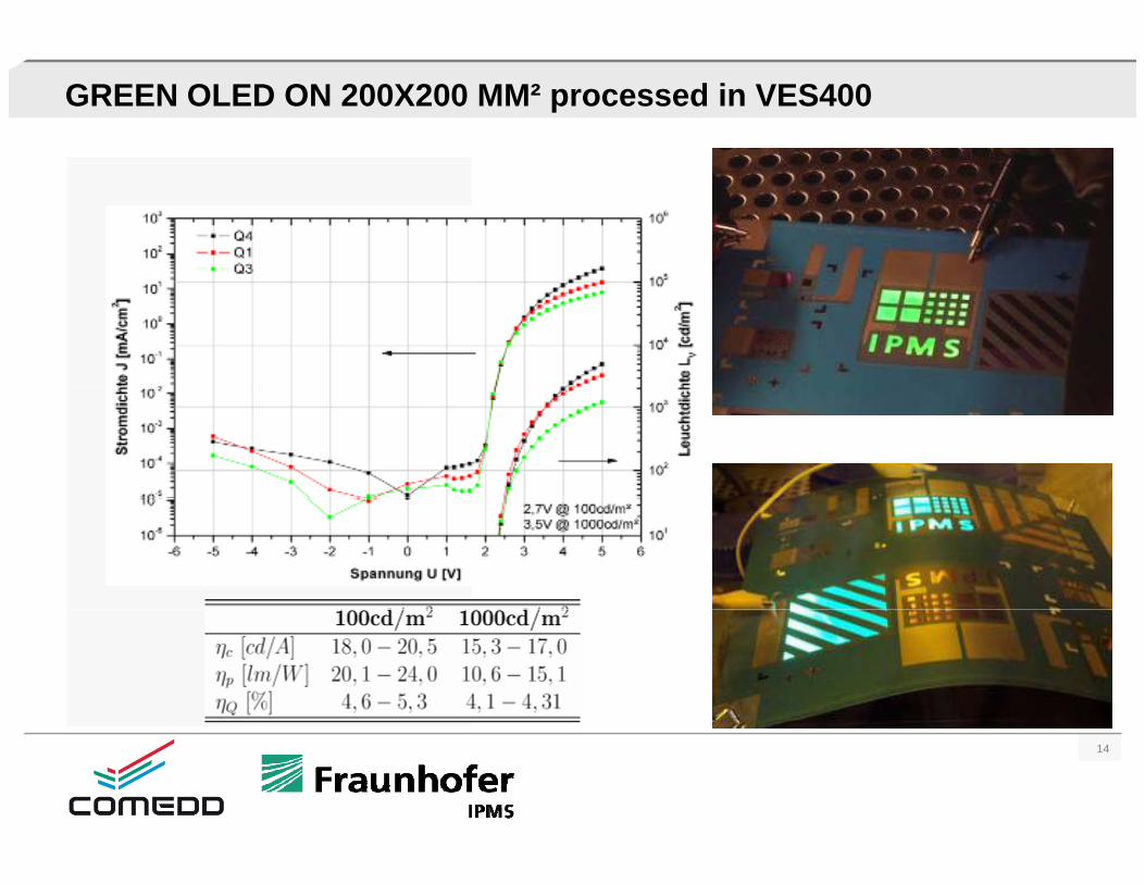
GREEN OLED ON 200X200 MM² processed in VES400
14

ROLL-TO-ROLL COATER FOR METAL STRIP
Batch type Roll-to-Roll CoaterSubstrate width 300 mm, thickness 0.2 … 0.5 mmPretreatment by ion beam and heatingPretreatment by ion beam and heating
Coating Stations:up to 9 novel linear evaporators for organic materials in total (5 double, 4 single)2 evaporators for metals1 DC/RF magnetron
organic materialEvaporationsources
ion beampretreatment
OLED-specific substrate handlingstrip guidance w/o front side roller contactun/rewinding with plastic liner
substrate and linerunwinding
transfer of coated substrate under inert atmosphere
metal evaporation sources
substrateand linerrewinding
magnetron
15
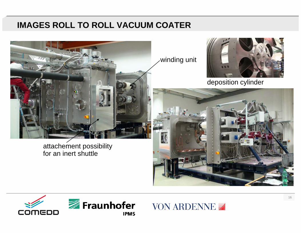
IMAGES ROLL TO ROLL VACUUM COATER
winding unit
deposition cylinder
attachement possibilityfor an inert shuttle
16
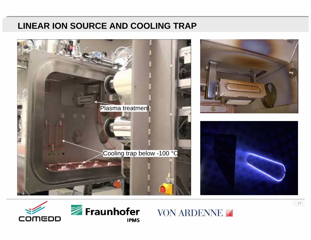
LINEAR ION SOURCE AND COOLING TRAP
Plasma treatment
Cooling trap below -100 °C
17
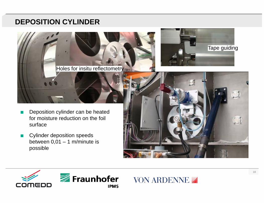
DEPOSITION CYLINDER
Tape guiding
Holes for insitu reflectometry
Deposition cylinder can be heated p yfor moisture reduction on the foil surface
Cylinder deposition speeds b t 0 01 1 / i t ibetween 0,01 – 1 m/minute is possible
18

NEW LINEAR EVAPORATION SOURCES FOR ORGANICS
horizontal orientation with rotatablehorizontal orientation with rotatable (360°) deposition tube enables deposition in top-down and bottom-up geometry
Organic evaporatorin the roll-to-rollcoater
new primary evaporator with distributed surface*
High rates at moderate t t ( d ddeposition tube (rotatable) temperatures (reduced degradation)
directly heated deposition tube with high temperature
deposition tube (rotatable)
shielding with high temperature homogeneity
scalable design
ll i t fill f iprimaryevaporator allows inert refill of organic
compounds
substrate
evaporator
shutter*Patent pending
19
p g
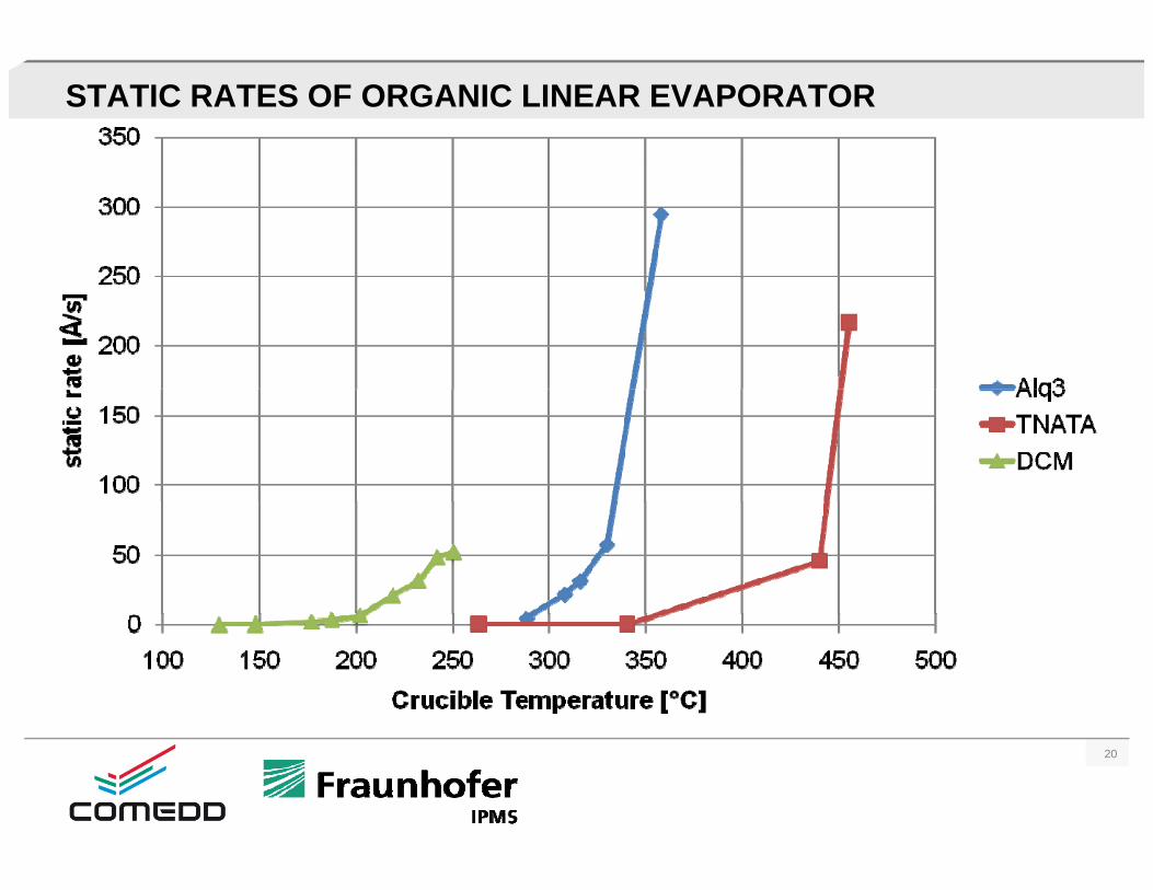
STATIC RATES OF ORGANIC LINEAR EVAPORATOR
20
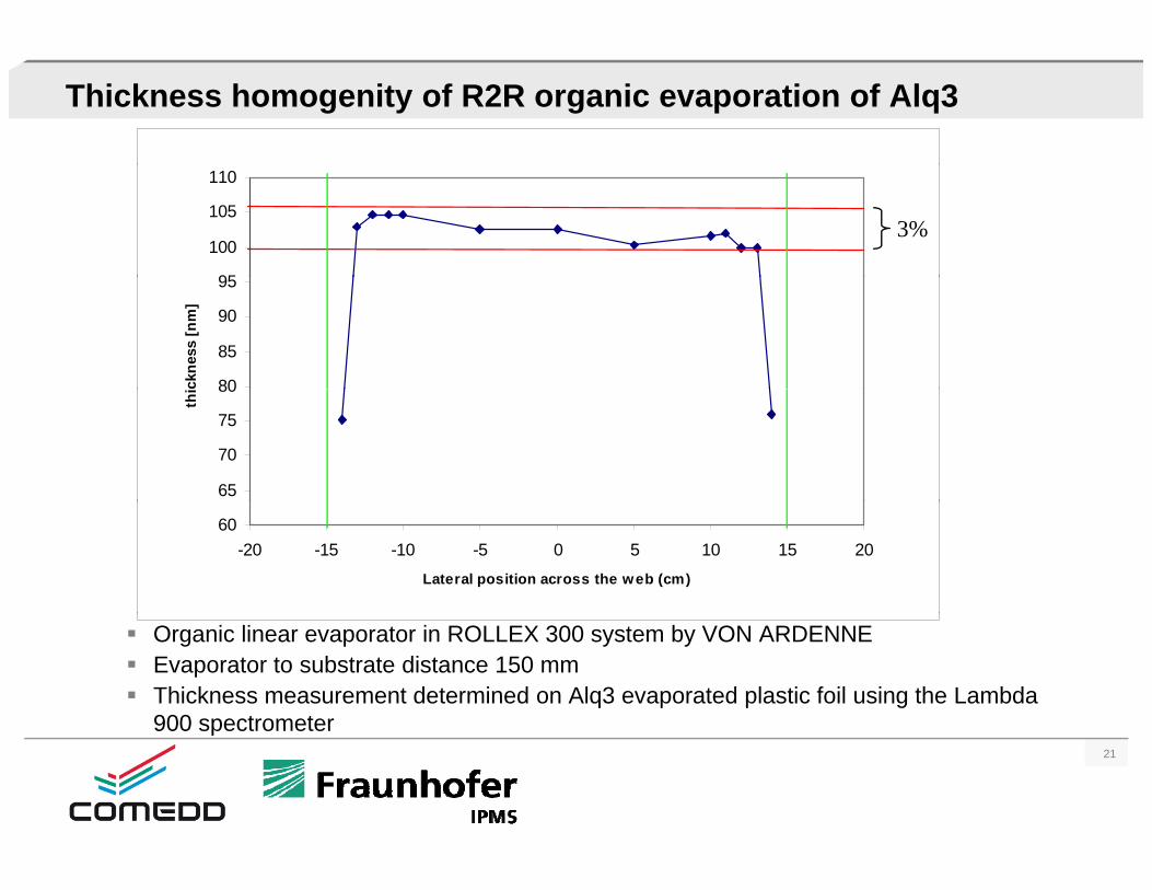
Thickness homogenity of R2R organic evaporation of Alq3
95
100
105
110
3%
80
85
90
95
ckne
ss [n
m]
65
70
75
80
thi
60-20 -15 -10 -5 0 5 10 15 20
Lateral position across the web (cm)
Organic linear evaporator in ROLLEX 300 system by VON ARDENNEEvaporator to substrate distance 150 mmThickness measurement determined on Alq3 evaporated plastic foil using the Lambda 900 spectrometer
21
900 spectrometer
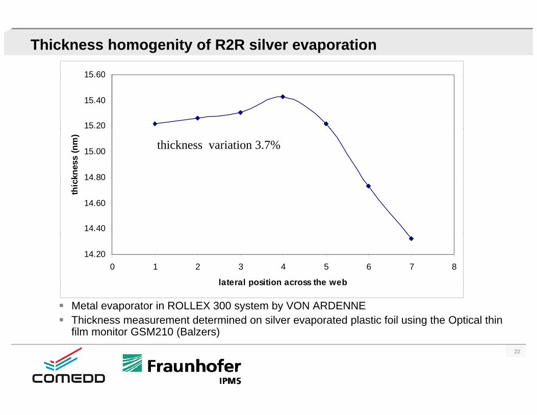
Thickness homogenity of R2R silver evaporation
15.60
15.20
15.40
15.60
14.80
15.00
ckne
ss (n
m)
thickness variation 3.7%
14.40
14.60
thic
14.200 1 2 3 4 5 6 7 8
lateral position across the web
Metal evaporator in ROLLEX 300 system by VON ARDENNEThickness measurement determined on silver evaporated plastic foil using the Optical thin film monitor GSM210 (Balzers)
p
22
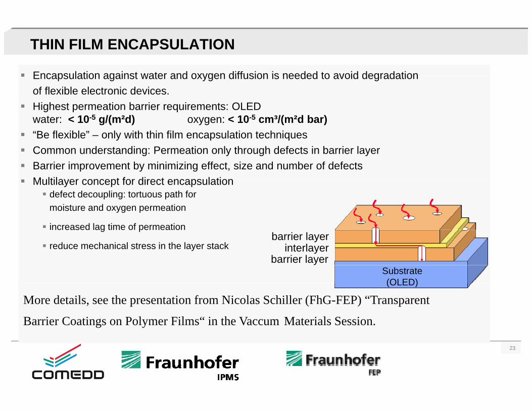
THIN FILM ENCAPSULATION
Encapsulation against water and oxygen diffusion is needed to avoid degradationEncapsulation against water and oxygen diffusion is needed to avoid degradation of flexible electronic devices.Highest permeation barrier requirements: OLED water: < 10-5 g/(m²d) oxygen: < 10-5 cm³/(m²d bar)“Be flexible” – only with thin film encapsulation techniquesCommon understanding: Permeation only through defects in barrier layerBarrier improvement by minimizing effect, size and number of defectsMultilayer concept for direct encapsulationMultilayer concept for direct encapsulation
defect decoupling: tortuous path formoisture and oxygen permeation
increased lag time of permeationg p
reduce mechanical stress in the layer stack interlayerbarrier layer
Substrate(OLED)
barrier layer
(OLED)
More details, see the presentation from Nicolas Schiller (FhG-FEP) “Transparent
Barrier Coatings on Polymer Films“ in the Vaccum Materials Session.
23
SUMMARY AND OUTLOOKTo fabricate large area lighting devices existing OLED display fabrication technologies have to be adapted in several aspectsadapted in several aspects
High efficient bottom emitting OLED on glass was shown
Highly efficient manufacturing
Low cost materialsLow cost materials
Metal strips and R2R deposition have potential for low cost production of lighting devices - First results promising
High efficient and stable top emitting OLED on metals substrates are possibleHigh efficient and stable top emitting OLED on metals substrates are possible
Unique approach for an OLED R2R coater using new evaporator concept
Promising results of thin film encapsulation
OutlookDevelopment of white OLED stack in R2R deposition process
Further developments in R2R thin film encapsulation
Roll-to-Roll process integration: cleaning, patterning, lamination
Implementation of R2R defect monitoring
Processes also to be used for Organic Solar Cells24
Processes also to be used for Organic Solar Cells
ACKNOWLEDGEMENT
All project members, especiallyM. Ammann, C. Rothe, Novaled
C. Deus, Von Ardenne
K. Leo, IAPP, TU Dresden
N. Schiller, J. Fahlteich, Fraunhofer FEP
J Drechsel CreaPhysJ. Drechsel, CreaPhys
This work is supported by the German Federal Ministry of Education and Research
Further Information: www.rollex-projekt.de
25