ROLAND A. LEVY - Information Services & Technologylevyr/resume2009.pdfFundamentals of Engineering...
21
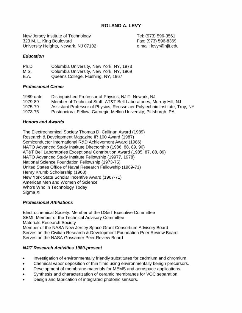
ROLAND A. LEVY New Jersey Institute of Technology Tel: (973) 596-3561 323 M. L. King Boulevard Fax: (973) 596-8369 University Heights, Newark, NJ 07102 e mail: [email protected] Education Ph.D. Columbia University, New York, NY, 1973 M.S. Columbia University, New York, NY, 1969 B.A. Queens College, Flushing, NY, 1967 Professional Career 1989-date Distinguished Professor of Physics, NJIT, Newark, NJ 1979-89 Member of Technical Staff, AT&T Bell Laboratories, Murray Hill, NJ 1975-79 Assistant Professor of Physics, Rensselaer Polytechnic Institute, Troy, NY 1973-75 Postdoctoral Fellow, Carnegie-Mellon University, Pittsburgh, PA Honors and Awards The Electrochemical Society Thomas D. Callinan Award (1989) Research & Development Magazine IR 100 Award (1987) Semiconductor International R&D Achievement Award (1986) NATO Advanced Study Institute Directorship (1986, 88, 89, 90) AT&T Bell Laboratories Exceptional Contribution Award (1985, 87, 88, 89) NATO Advanced Study Institute Fellowship (19977, 1978) National Science Foundation Fellowship (1973-75) United States Office of Naval Research Fellowship (1969-71) Henry Krumb Scholarship (1968) New York State Scholar Incentive Award (1967-71) American Men and Women of Science Who's Who in Technology Today Sigma Xi Professional Affiliations Electrochemical Society: Member of the DS&T Executive Committee SEMI: Member of the Technical Advisory Committee Materials Research Society Member of the NASA New Jersey Space Grant Consortium Advisory Board Serves on the Civilian Research & Development Foundation Peer Review Board Serves on the NASA Gossamer Peer Review Board NJIT Research Activities 1989-present Investigation of environmentally friendly substitutes for cadmium and chromium. Chemical vapor deposition of thin films using environmentally benign precursors. Development of membrane materials for MEMS and aerospace applications. Synthesis and characterization of ceramic membranes for VOC separation. Design and fabrication of integrated photonic sensors.
-
Upload
truongtram -
Category
Documents
-
view
217 -
download
4
Transcript of ROLAND A. LEVY - Information Services & Technologylevyr/resume2009.pdfFundamentals of Engineering...
ROLAND A. LEVY New Jersey Institute of Technology Tel: (973) 596-3561 323 M. L. King Boulevard Fax: (973) 596-8369 University Heights, Newark, NJ 07102 e mail: [email protected]
Education
Ph.D. Columbia University, New York, NY, 1973 M.S. Columbia University, New York, NY, 1969 B.A. Queens College, Flushing, NY, 1967
Professional Career 1989-date Distinguished Professor of Physics, NJIT, Newark, NJ 1979-89 Member of Technical Staff, AT&T Bell Laboratories, Murray Hill, NJ 1975-79 Assistant Professor of Physics, Rensselaer Polytechnic Institute, Troy, NY 1973-75 Postdoctoral Fellow, Carnegie-Mellon University, Pittsburgh, PA
Honors and Awards The Electrochemical Society Thomas D. Callinan Award (1989) Research & Development Magazine IR 100 Award (1987) Semiconductor International R&D Achievement Award (1986) NATO Advanced Study Institute Directorship (1986, 88, 89, 90) AT&T Bell Laboratories Exceptional Contribution Award (1985, 87, 88, 89) NATO Advanced Study Institute Fellowship (19977, 1978) National Science Foundation Fellowship (1973-75) United States Office of Naval Research Fellowship (1969-71) Henry Krumb Scholarship (1968) New York State Scholar Incentive Award (1967-71) American Men and Women of Science Who's Who in Technology Today Sigma Xi
Professional Affiliations Electrochemical Society: Member of the DS&T Executive Committee SEMI: Member of the Technical Advisory Committee Materials Research Society Member of the NASA New Jersey Space Grant Consortium Advisory Board Serves on the Civilian Research & Development Foundation Peer Review Board Serves on the NASA Gossamer Peer Review Board
NJIT Research Activities 1989-present
Investigation of environmentally friendly substitutes for cadmium and chromium.
Chemical vapor deposition of thin films using environmentally benign precursors.
Development of membrane materials for MEMS and aerospace applications.
Synthesis and characterization of ceramic membranes for VOC separation.
Design and fabrication of integrated photonic sensors.
2
Synthesis and characterization of dielectric (SiO2, Si3N4, SiC, BN, DLC) and metal (TiN, Cu, W, Al) thin films.
Evaluation of non-global warming gases for chamber cleaning/wafer patterning.
Multi-lifecycle reengineering of CRT glass.
NJIT Graduate Theses “Synthesis and Characterization of Atmospheric Pressure Chemically Vapor Deposited Aluminum”, Sipeng Gu, Ph.D. in Material Science (2008). “Synthesis and Characterization of Plasma Enhanced Chemically Vapor Deposited Tantalum Films”, Weizhong Chen, Ph.D. in Physics (2008). “Modeling of Boron and Phosphorus Implantation of (100) Germanium and Investigation of Dopant Annealing Behavior”, Yong Seok Suh, Ph.D. in Materials Science (2004). “Fabrication and Characterization of Microcrystalline Silicon Solar Cells”, Liwei Li, Ph.D. in Materials Science (2003). “Development of An Integrated Photonic Sensor for Monitoring Hazardous Organics”, Dianhong Luo, Ph.D. in Materials Science, (2001). “Synthesis and Characterization of Low Pressure Chemically Vapor Deposited Boron Nitride and Titanium Nitride Films”, Narahari Ramanuja, Ph.D. in Materials Science (2000). “Nanoporous SiO2/Vycor Membranes for Air Separation”, Mihir Tungare. M.S. in Materials Science (2000). “Low Pressure Chemical Vapor Deposition of Titanium Nitride: Synthesis and Characterization”, Sameer Dharmadhikari, M.S. in Chemical Engineering (1999). “Synthesis and Characterization of Silicon Dioxide films Using Diethylsilane and Oxygen”, Kiran Kumar, M.S. in Materials Science (1998). “Plasma Enhanced Chemical Vapor Deposition Of Diamond Like Carbon Films Using Acetylene”, Sriram Vishwanathan, M.S. in Materials Science (1998). “Low Pressure Chemical Vapor Deposition of Boron Nitride Thin Films from Triethylamine Borane Complex and Ammonia”, Narahari Ramanuja, M.S. in Materials Science (1997). “The In0.75Ga0.25As/In0.52Al0.48As/InP Hall Effect Magnetic Field Sensor”, Oleg Mitrofanov, M.S. in Materials Science (1997). “Development and Characteristics of Carbon Nitride Thin Solid Films for Advanced Coating Applications”, Muhammad Hussain, M.S in Chemical Engineering (1997). “Synthesis and Characterization of Phosphosilicate Glass films by LPCVD for Sensor Applications”, Hui Wu, M.S. in Materials Science (1997). “Synthesis and Characterization of LPCVD Silicon Carbide Films Using Novel Precursors”, Mahalingam Bhaskaran, Ph.D. in Materials Science (1997).
3
“Low Pressure Chemical Vapor Deposition of SiO2 on Porous Vycor Tubes for Gas Separation”, Emmanuel Ramos, Ph.D. in Chemistry (1996). “Microporous Silicon Dioxide /Vycor Membranes for Gas Separation”, Justin Barone, M.S. in Materials Science (1996). “Trifluoroiodomethane as an Environmentally Friendly Gas for Wafer patterning by Plasma Etching Process”, Krit Aryusook, M.S. in Materials Science (1996). “Synthesis and Characterization of Silicon Dioxide Thin Films by Low Pressure Chemical Vapor Deposition”, Sutham Niyomwas, M.S. in Materials Science (1996). “Synthesis and Characterization of Hafnium Carbide Thin Films”, Wiriya Thongruang, M.S. in Materials Science (1996). “Synthesis and Characterization of Silicon Dioxide Thin Films by Low Pressure Chemical Vapor Deposition Using Ditertiarybutylsilane and Oxygen”, Sung Jun Lee, M.S. in Materials Science (1996). “Low Pressure Chemical Vapor Deposition of Silicon Dioxide and Phosphosilicate Glass Thin Films”, Vijayalakshmi Venkatesan, M.S. in Materials Science (1996). “Fabrication of Integrated Optic Sensor to Monitor Pollutant Concentration in Effluents”, Kiran Chatty, M.S. in Materials Science (1996). “Characterization of Low Pressure Chemically Vapor Deposited Boron Nitride Films as Low Dielectric Constant ILD Materials”, Manish Narayan, M.S. in Engineering Science (1996). “Plasma Enhanced Chemical Vapor Deposition of Stress Free Tungsten Films”, David Perese, M.S. in Engineering Science (1996). “Synthesis of Boron Nitride/VYCOR Composite Membrane Structures by an Optimized LPCVD Process”, Ravindranath Chenna, M.S. in Engineering Science (1995). “Low Pressure Chemical Vapor Deposition of Tungsten for X-ray Lithography Applications”, Hong Yu Chen, M.S. in Engineering Science (1995). “Low Pressure Chemical Vapor Deposition of Silicon Nitride Films from Trimethyl-aminosilane”, Xin Lin, M.S. in Engineering Science (1995). “Low Pressure Chemical Vapor Deposition of Copper Films from Cu(I) (HFAC) (TMVS)”, Wei-Shang King, M.S. in Engineering Science (1995). “Synthesis of Silicon Oxide/VYCOR Composite Membrane Structures by an Optimized LPCVD Process”, Abhijit Datta, M.S. in Engineering Science (1995). “The Photolithographic Patterning of Porous Silicon using Silicon Nitride and Silicon Carbide Films as Masks”, Hong Wang, M.S. in Engineering Science (1995). “Synthesis and Characterization of Silicon Dioxide Thin Films by Plasma Enhanced Chemical deposition from Diethylsilane and Nitrous Oxide”, Lan Chen, M.S. in Chemistry (1995). “Low Pressure Chemical Vapor Deposition of Silicon Nitride Films from Ditertiary-butylsilane”, Xiangqun Fan, M.S. in Engineering Science (1994).
4
“Laser Treatment of Ceramic Coatings on Defective Ceramic Glazed Tile”, Gousinn Yu, M.S. in Engineering Science (1993). “Synthesis and Characterization of Silicon Nitride Films Deposited by Plasma Enhanced Chemical Vapor Deposition using Diethylsilane”, Yanyao Yu, M.S. in Engineering Science (1993). “Synthesis and Characterization of LPCVD Boron Nitride Films for X-Ray Lithography”, Wen-Pin Kuo, M.S. in Engineering Science (1992). “Low Temperature Synthesis and Characterization of Silicon Dioxide Films by LPCVD Using Diethylsilane”, Chakravarthy S. Gorthy, M.S. in Engineering Science (1992). “Characterization of LPCVD Deposited Silicon Dioxide Thin Films”, Xue Du, M.S. in Chemistry (1992). “Synthesis and Characterization of Silicon Nitride Films Deposited by Plasma Enhanced Chemical Vapor Deposition", Kei Turng Shih, M.S. in Electrical Engineering (1991). “Low Pressure Chemical Vapor Deposition (LPCVD) of Silicon Carbide from Diethylsilane”, Yi-Tong Shi, M.S. in Chemistry (1991). “Synthesis and Characterization of Boron Nitride Masks for X-Ray lithography”, Venkat Paturi, M.S. in Electrical Engineering (1991). “Synthesis and Characterization of LPCVD Silicon Carbide Thin Films for X-Ray Lithography”, Mahalingam Bhaskaran, M.S. in Electrical Engineering (1991).
Sponsored Post-Doctoral Fellows Sungmin Maeng, Yong S. Suh, Sipeng Gu, Raul J. Martin Palma, Vitaly Sigal, Vladimir Zaitsev, Oktay Gokce, Jose M. Albella, Jan Opyrchal, Eric Mastromatteo.
Consulting
Lawrence Livermore EPV ENECO Rice Systems IBM Allied Signal Motorola Heraeus Amersil Olin Schumacher Kulite Nanostructures Inc. Process Technology Limited Cypress Semiconductors EM Industries Thin Films Concepts Lucent technologies Analog Devices Structured Materials Industries Sharp Microelectronics Texas Instruments Veeco Instruments Naval Research Laboratory Mems Optical Plasmion Schutz Engineering
Professional Service
Reviewer for the Journal of The Electrochemical Society, the Journal of Material Science, the Journal of Applied Physics, and the Journal of Non-Crystalline Solids.
Serves on the National Science Foundation Review Boards.
5
Reviewer of NSF, DOE, EPSCOR proposals.
Member of the Associated Institutions for Material Sciences Advisory Board.
Member of the NASA New Jersey Space Grant Consortium Advisory Board.
Teaching Activities Freshman Physics Solid State Physics Modern Physics Materials Science
Curricula Development Curricula for the following new courses were developed and implemented within the NJIT Materials Science and Engineering program: Fundamentals of Engineering Materials Mechanical Properties of Materials Composite Materials Introduction to Ceramics Glass Science and Engineering Thermodynamics of Solids Transport of Electrons and Phonons in Solids Physical Metallurgy Diffusion and Solid State Kinetics Crystallography and Diffraction Science and Technology of Thin Films Defects in Solids Materials Characterization Materials Science and Engineering
Funded Programs: “Investigation of Chemically Vapor Deposited Tantalum for Medium Caliber Gun Barrel Protection”, Strategic Environmental Research and Development Program, February 2005 to January 2008 ($1,500,000). “Investigation of Chemically Vapor Deposited Aluminum as a Replacement Coating for Cadmium”, Strategic Environmental Research and Development Program, September 2004 to August 2007 ($1,500,000). “Microcrystalline Silicon Photovoltaic devices”, Department of Energy, May 2000 to April 2003 ($600,000). “An Integrated Near Infrared Spectroscopy Sensor for In-situ Environmental Monitoring”, U. S. Environmental Protection Agency, March 1998 to February 2001 ($551,570). “Multi-lifecycle engineering of CRT Glass”, New Jersey Commission on Science and Technology, January 1998 to December 1999 ($128,000). “An Integrated Evanescent Wave Absorbance Sensor for In-situ Monitoring and process Control Leading to Reduction of Hazardous Emissions”, U. S. Army, October 1997 to September 1999 ($235,000). “Design And Characterization of Ceramic Membrane Modules for VOC Separation”, NJIT Hazardous Substance Management Research Center, July 1997 to June 1998 ($61,861). “An Integrated Optical Sensor for Environmental Monitoring”, NJIT Hazardous Substance Management Research Center, July 1996 to June 1997 ($36,000). “Design And Characterization of Ceramic Membrane Modules for VOC Separation”, NJIT Hazardous Substance Management Research Center, July 1996 to June 1997 ($64,000).
6
“Synthesis and Characterization of Carbon Nitride Films”, New Jersey Space Grant Consortium, August 1995 to August 1996 ($25,000). “Microsensor for Monitoring Volatile Organics from Thermoplastics Using Pulsed Terahertz Spectroscopy”, Center for Manufacturing Systems, July 1995 to June 1996 ($20,000). “An Integrated Optical Sensor for Environmental Monitoring”, Hazardous Substance Management Research Center, June 1995 to June 1997 ($102,000). “Novel Ceramic Membranes for VOC Separation”, Emission Reduction Research Center, July 1994 to June 1995 ($81,000). “Synthesis and Characterization of Ceramic Membranes for VOC Separation”, Hazardous Substance Management Research Center, July 1994 to June 1996 ($160,000). “Synthesis and Characterization of Silicon Carbide Membranes for X-Ray Lithography”, ARPA, October 1992 to September 1995, ($290,000). “Micromechanical Characterization of Ceramic Coatings”, NASA New Jersey Space Grant Consortium, September 1992 to August 1993 ($25,000). “Plasma Enhanced Chemical Vapor Deposition of Silicon Nitride from Di-t-butylsilane”, Center for Manufacturing Systems, September 1992 to August 1993 ($25,000). “Novel Ceramic Membranes for VOC Separation”, Air Emission Reduction Center, January 1992 to June 1993 ($210,833). “Silicon Carbide films for Aerospace Applications”, NASA New Jersey Space Grant Consortium, September 1991 to August 1992 ($24,899). “Synthesis and Characterization of SiC and BN Films for Microengineering Structures”, Advanced Technology Center on Surface Engineered Materials, June 1991 to May 1992 ($14,295). “Microelectronic Deposition Processes Based on safe Substitutes for Hazardous Precursors”, Hazardous Substance Management Research Center, September 1990 to August 1991 ($72,034). “Synthesis and Characterization of Boron Nitride Masks for X-Ray lithography”, NSF, August 1990 to July 1992 ($88,168). “Fabrication of Thin Film Phosphors for High Performance Cathode Ray Tubes”, Center for Manufacturing Systems, July 1990 to June 1991 ($8,000). “Synthesis and Characterization of Silicon Carbide and Oxide Films”, Research Corporation, May 1990 to August 1991 ($22,500). “A Boron Nitride Mask manufacturing for X-Ray Lithography”, Center for Manufacturing Systems, March 1990 to June 1991 ($37,500).
Industrial Experience - AT&T Bell Laboratories 1979-89
Direct participation in all aspects of VLSI fabrication as related to the development of the 2.5 m
and 1.25 m TWIN-TUB CMOS-technology
Process tailoring of all major IC operations.
7
Initiation of novel LPCVD processes for dielectric insulation, as well as gate, contact, and interconnect metallization.
Implementation of advanced materials and processes in IC device manufacturing.
Application of diagnostic techniques for characterization of materials and analysis of circuit structures.
Assessment of materials performance as pertaining to device yield and reliability.
Development of new mask fabrication technologies for submicron x-ray lithography.
Design and Processing of integrated photonic circuits on silicon.
Development of new applications for high Tc superconductors.
Academic Experience - CMU and RPI 1973-79
Investigation of the structure of silicate glasses with a variety of diagnostic techniques including Mossbauer spectroscopy, electron paramagnetic resonance, and x-ray diffraction.
Characterization of the structure and electrical properties of amorphous alloys at cryogenic temperatures.
Evaluation of the magnetic and electrical properties of Pd-Ag-Fe alloys and correlation with theoretical models.
Industrial consulting with local industries has resulted in research finding of the following projects:
Solar Energy Converters Lead Shot Replacement Magnetic Bubbles Light Modulation by Thin Films Triggering Mechanisms for Photoresists Thermodynamics for Lighting Powder Metallurgy of Composites Acousto-Optic Bulk Waves Ceramic Forming Processes Investigation of Phase Separation in a Lead Borosilicate Glass
RPI Teaching Activities Freshman-Sophomore Physics Experimental Physics I and II Applied Solid State Physics Special Projects in Physics Advanced Solid State Physics Materials I Materials and Processes Principles and Applications of Mossbauer Effect Spectroscopy
RPI Departmental Committees
Chairman, Solid State Seminar (1976-1977)
Member of Undergraduate Majors Committee (1976-1977)
Member of Qualifying Exam Committee (1977-1978)
Radiation Safety Officer (1975-1978)
French Language Examiner (1975-1978)
RPI Consulting GTE Laboratories Lawrence Berkeley Laboratories Watervliet Arsenal Mechanical Technologies Inc. Xerox Corporation IBM
8
RRC International Combustion Engineering General Electric
Books “Materials and Processes for Submicron Technologies”, Elsevier, New York, (1999). “Novel Silicon Based Technologies”, Kluwer Academic Publishers, Boston, Massachusetts (1991). “Reduced Thermal Processing for ULSI”, Plenum Publishing Corporation, New York (1989). “Microelectronic Materials and Processes”, Kluwer Academic Publisher, Boston, Massachusetts (1989). “Multilevel Metallization and Packaging”, The Electrochemical Society, Pennington, New Jersey (1985). “Electrical Magnetic and Optical Properties of Glasses”, North-Holland Publishing Company, New York (1980). “Amorphous Magnetism II”, Plenum Publishing Corporation, New York (1977).
Videotapes Novel Silicon Based Technologies (1991) This video course production covers the following topics: Gallium Arsenide Heteropitaxial Growth on Silicon, Device Applications of Epitaxial Gallium Arsenide on Silicon, Ion Beam Synthesis in Silicon, Ion Beam Processing of CVD Silicon Layers, Technology and Devices for Silicon Based Three-Dimensional Circuits, Integrated Fabrication of Micromechanical Structures on Silicon, Micromachining of Silicon for Sensor Devices, Preparation and Properties of High Temperature Superconductors, Integrated Photonic Circuits on Silicon, Principles and Implementation of Artificial Neural Networks. Reduced Thermal Processing for ULSI (1989) This video course production covers the following topics: RTP with Reactive Gases, Silicidation by RTA, Microstructural Defects in RTP IC Materials, RTP Systems, RTP Integration, Laser Pantography, Ion Beam Assisted Processing , Micrometallization Technologies, Multilevel Interconnect Structures, Interlevel Dielectrics for RTP, CVD of Metals and Low Temperature Silicon Epitaxy. Microelectronic Materials and Processes (1987) This video course production covers the following topics: Crystal Growth, Epitaxy, Silicon Oxidation, Physical Vapor Deposition, Chemical Vapor Deposition, Dielectrics, Silicides for VBI Applications, Resist Materials, Fine-Line lithography, Dry Etching Processes, Ion Implantation, Diffusion in Semiconductors, Interconnect Materials, Imperfections and Impurities in Semiconductors, Process Simulation, Diagnostic Techniques for Microelectronic Materials, and Packaging.
Satellite Course Advanced Materials and Processing for the ULSI Era (1991)
9
This satellite course production covers the following topics: High-Speed, High-Performance Devices, Thin Films for Future Generation ICs, Submicron Lithographic Technologies, ULSI Process Integration, Advanced Plasma Processes, Microelectronic Packaging Technologies for Leading-Edge Consumer Electronics Products.
Publications X.Q. Yi, K. Su, E. Schlam, and R. A. Levy, “Electrostatic Flexible Film Based Smart Window; Optical
design, Performance and Residual Charge Investigation”, Sol. Energy, 110, 67 (2014). X. Q. Yi and R. A. Levy, “Electrical Breakdown Mechanism
in Contaminated Polyimide Coating”, Emer. Mater. Res. 4, 1 (2014). Y. Suh, W. Chen, S. Maeng, S. Gu, R. A. Levy, H. Thridandam, “Synthesis and Characterization of Plasma Assisted Chemically Vapor Deposited Tantalum”, submitted to J. of Surface and Coatings Technology (2009). S. Gu, S. Maeng, R. A. Levy, and Y. Suh, “Investigation of Atmospheric Pressure Chemically Vapor Deposited Aluminum Coatings for Corrosion Protection”, submitted to J. of Surface and Coatings Technology (2009). Y. Suh, W, Chen, S. Maeng, R. Levy, H. Thridandam, K. Cuthill, T. Gaffney, “Investigation of Plasma Enhanced Chemically Vapor Deposited Tantalum on High Strength Steels”, Materials Science and Technology 2007 Conference Proceedings, pp 563-572 (2007). S. Maeng, S. Gu, R. Levy, F. Gomez, S. Newberg, D. Deavenport, E. Brooman, E. Berman, J. Beatty, “Synthesis and Characterization of Atmospheric Pressure Chemically Vapor Deposited Aluminum”, Materials Science and Technology 2007 Conference Proceedings, pp 67-77 (2007). Y. S. Suh, M. S. Carroll, R. A. Levy, G. Bisognin, D. De Salvador, and M. A. Sahiner, “Implantation and Activation of High Concentrations of Boron and Phosphorus in Germanium”, Mater. Res. Soc. Symp. Proc., Vol. 891, 891 (2006).
M. S. Carroll, Y. S. Suh, and R. A. Levy, “Suppressed Boron Diffusion in Bulk Silicon below Strained (100) Si1-xGex Surfaces during Nitrogen Annealing”, Proc. of the Electrochem. Soc. Vol. 501, 675 (2006). M. S. Carroll, Y. S. Suh, and R. A. Levy, “Suppressed Boron Diffusion in Bulk Silicon below Strained (100) Si1-xGex Surfaces during Nitrogen Annealing”, to appear in Conference Proceedings of the Electrochemical Society (2005). Y. M. Li, L. Li, J. A. Anna Selvan, A. E. Delahoy, and R. A. Levy, “Effects of Seeding Methods on the Fabrication of Microcrystalline Silicon Solar Cells using Radio Frequency Plasma Enhanced Chemical
Vapor Deposition”, Thin Solid Films, vol. 483, 84 (2005). Y. S. Suh, M. S. Carroll, R. A. Levy, M. A. Sahiner, G. Bisognin, and C. A. King, “Modeling of Boron
and Phosphorus Implantation into (100) Germanium”, IEEE Trans. Electron Devices, vol. 52, 91 (2005). Y. S. Suh, R. A. Levy, M. S. Carroll, and A. Sahiner, “Phosphorus and Boron Implantation into (100)
Germanium”, Mater. Res. Soc. Symp. Proc., vol. 809, B8.11.1 (2004).
10
L. Li, Y. M. Li, J. A. Anna Selvan, A. E. Delahoy, and R. A. Levy, “Correlations between Structural Properties and Performance of Microcrystalline Silicon Solar Cells Fabricated by Conventional RF-
PECVD”, J. Non-Cryst. Solids 347, 106 (2004). Y. M. Li, J. A. Anna Selvan, L. Li, R. A. Levy, and A. E. Delahoy, “A Study of Single chamber RF-PECVD µc-Si Solar Cells”, Proceedings of the Third World Conference on Photovoltaic Energy Conversion, Osaka, Japan, 1788 (2003). L. Li, Y. M. Li, J. A. Anna Selvan, A. E. Delahoy, and R. A. Levy, “Structural Characterizations of Microcrystalline Silicon Solar Cells Fabricated by Conventional RF-PECVD”, Mater. Res. Soc. Symp.
Proc., vol. 762, A5.15.1 (2003). D. H. Luo, R. A. Levy, Y. F. Hor, and J. F. Federici, and R. M. Pafchek, “An Integrated Photonic
Sensor for In-situ Monitoring of Hazardous Organics”, Sens. & Actuators B 92, 121 (2003). N. Ramanuja, R. A. Levy, S. N. Dharmadhikari, E. Ramos, C. W. Pearce, S. C. Menasian, P. C. Schamberger, and C. C. Collins, “Synthesis and Characterization of Low Pressure Chemically Vapor
Deposited Titanium Nitride Films Using TiCl4 and NH3”, Mater. Lett., 57, 261 (2002). R. A. Levy, L. Chen, J. M. Grow, and Y. Yu, “Plasma Enhanced Chemical Vapor Deposition Of Si-O-
H And Si-N-C-H Films Using The Environmentally Benign Precursor Diethylsilane”, Mater. Lett., 54, 102 (2002). R. J. Martin-Palma, J. M. Martinez-Duart, L. Li, and R. A. Levy, “Electrical Behavior of Double-Sided
Metal/Porous Silicon Structures for Optoelectronic Devices”, Mater. Sci. Eng. C 19, 359 (2002). A. Avila, I. Montero, L. Galán, J. M. Ripalda, J. M. Martinez-Duart, and R. A. Levy, “Silicon Carbide
Thin Films obtained by Chemical Vapor Deposition: An XPS Study”, J. of Applied Physics, 89, 212 (2001). N. M. Ravindra, F. M. Tong, D. Pattnaik, D. Ivanov, R. A. Levy, K. Aryusook, and V. Patel, “Silicon
Microlenses for IR Image Sensors”, Proc. SPIE, Santa Clara, CA, vol. 3511, 152 (1998). R. A. Levy, V. B. Zaitsev, K. Aryusook, C. Ravindranath, V. Sigal, A. Misra, S. Kesari, D. Ruffin, J. Sees, and L. Hall, “Investigation of CF3I as an Environmentally Benign Dielectric Etchant”, J. Mater.
Res., 13, 2643 (1998). A. Misra, J. Sees, L. Hall, R. A. Levy, V. B. Zaitsev, K. Aryusook, C. Ravindranath, V. Sigal, S. Kesari, and D. Rufin, “Plasma Etching of dielectric Films Using the Non-Global -Warming gas CF3I”, Mater.
Lett., 34, 415 (1998). L. Vazquez, R. C. Salvarezza, E. Albano, A. J. Arvia, A. H. Creus, R. A. Levy, and J. M. Albella, “Surface Morphology Evolution of Chemical vapor Deposited Tungsten Films on Si(100)”, Chem. Vap.
Deposition 4, 89 (1998). S. Gilles, N. Bourhila, J. P. Senateur, R. Madar, R. A. Levy, and E. Blanquet, “Deposition of Ti(C,N)
Thick Films by ILPCVD Starting from TDMAT”, Proc. Mater. Res. Soc., Boston, MA, vol. 495, 177 (1998). R. A. Levy, C. Ravindranath, L. N. Krasnoperov, J. Opyrchal, and E. S. Ramos, “Porous Vycor Membranes Modified by Chemical Vapor Deposition of Boron Nitride for Gas Separation”, J.
Electrochem. Soc., 144, 349 (1997).
11
R. A. Levy, E. S. Ramos, L. N. Krasnoperov, A. Datta, and J. M. Grow, “Nanoporous SiO2/Vycor
Membranes for Gas Separation”, J. Mater. Res. 11, 3164 (1996). R. A. Levy, X. Lin, J. M. Grow, H. J. Boeglin, and R. Shalvoy, “Low Pressure Chemical Vapor Deposition of Silicon Nitride Using the Environmentally Friendly Tris(dimethylamino)silane Precursor”,
J. Mater. Res., 11, 1483 (1996). L. Vasquez, J. M. Albella, A. J. Arvia, R. C. Salvarezza, R. A. Levy, and D. Perese. “Roughening
Kinetics of Chemical Vapor Deposited Copper Films on Si(100)”, Appl. Phys. Lett., 68, 1285 (1996). R. A. Levy, J. M. Grow, Y. Yu, and K. T. Shih, “Plasma Enhanced Chemical Vapor Deposition of Si-N-
C-H Films from Environmentally Benign Organosilanes”, Mater. Lett., 24, 47 (1995). J. M. Grow, R. A. Levy, X. Fan, and M. Bhaskaran, “Growth Kinetics and Characterization of Low
Pressure Chemically Vapor Deposited Si3N4 Films from (C4H9)2SiH2 and NH3”, Mater. Lett., 23, 187 (1995). H. Wang, B. Welker, Y. Gao, J. F. Federici, and R. A. Levy, “Photolithographic Patterning of Porous
Silicon Using Silicon Nitride and Silicon Carbide Masks”, Mater. Lett., 23, 209 (1995).
R. A. Levy and J. M. Grow, “Improved Tools for Microelectronic Processes”, NJIT Research, vol. 3, 17 (1995). R. A. Levy, E. Mastromatteo, J. M. Grow, V. Paturi, W. P. Kuo, H. J. Boeglin, and R. Shalvoy, “Low Pressure Chemical Vapor Deposition of B-N-C-H Films from Triethylamine Borane Complex”, J. Mater.
Res., 10, 320 (1995). R. A. Levy, J. M. Grow, Y. Yu, and K. T. Shih, “Plasma Enhanced Chemical Vapor Deposition of Silicon Nitride from Novel Organosilanes”, in “Materials and Processes for Environmental Protection”,
Materials Research Society Symposium Proceedings, Vol. 344, Pittsburgh, PA (1994). J. M. Grow and R. A. Levy, “Micromechanical Characterization of Chemically Vapor Deposited
Ceramic Films”, J. Mater. Res., 9, 2072 (1994). R. A. Levy, J. M. Grow, and C. S. Chakravarthy, “Low Temperature Synthesis and Characterization of
Silicon Dioxide Films”, Chem. Mater., 5, 1710 (1993). R. A. Levy and J. M. Grow, “LPCVD of Silicon carbide from the Organosilanes Diethylsilane and Di-t-butylsilane”, in “Material Aspects of X-ray Lithography”, Eds. G. K. Celler and J. R. Maldonado,
Materials Research Society Symposium Proceedings, Vol. 306, pp. 219-228, Pittsburgh, PA (1993). J. M. Grow, R. A. Levy, M. Bhaskaran, H. J. Boeglin, and R. Shalvoy, “Low Pressure Chemical Vapor
Deposition of Silicon Carbide from Diteriarybutylsilane”, J. Electrochem. Soc., 140, 3001 (1993). R. A. Levy and J. M. Grow, “Growth Kinetics and Properties of Dielectric Films Synthesized from
Diethylsilane”, Mater. Sci. & Eng., B17,172 (1993). J. M. Grow, R. A. Levy, Y. T. Shi, and R. L. Pfeffer, “Low Pressure Chemical Vapor Deposition of
Silicon Carbide Using Diethylsilane”, J. Electrochem. Soc., 140, 851 (1993).
12
“Novel Silicon Based Technologies”, Ed. by R.A. Levy, Kluwer Academic Publishers, Dordrecht, The Netherlands (1991). F. Schrey, P. K. Gallagher, and R. A. Levy, “Selective Silicide or Boride Film Formation by Reaction
of Vapor Phase TiCI4 with Silicon or Boron”, J. Electrochem. Soc., 137, 1647 (1990). “Reduced Thermal Processing for ULSI”, Ed. by R.A. Levy, Plenum Press, New York (1990). “Microelectronic Materials and Processes”, Ed. by R.A. Levy, Kluwer Academic Publishers, Boston, Massachusetts (1989).
T. M. Duncan, R. A. Levy, and P. K. Gallagher, “Structural Characterization of Boron Nitride Films”, J.
Appl. Phys., 64, 2990 (1988). R. A. Levy, D. J. Resnick, R. C. Frye, A. W. Yanof, G. M. Wells, and F. Cerrina, “An Improved Boron
Nitride Technology for X-Ray Masks”, J. Vac. Sci. & Technol., B6, 154 (1988). R. A. Levy, “Planarization Techniques for Interlevel Dielectric Applications”, Proc. SEMICON/Japan'87 Technical Symposium, Tokyo, Japan (1987). R. A. Levy and T. Y. Kometani, “Analysis of Borophosphosilicate Glass Films by Inductively Coupled
Plasma-Atomic Emission Spectroscopy”, J. Electrochem. Soc., 134, 1565 (1987). R. A. Levy, P. K. Gallagher, and F. Schrey, “Low Pressure Chemical Vapor Deposition of Borophosphosilicate Glass Films Produced by Injection of Miscible DADBS-TMB-TMP Liquid
Sources”, J. Electrochem. Soc., 134, 1744 (1987). R. A. Levy, “The Future Outlook of Semiconductor Materials and Processes in VLSI Fabrication”, Proc. of SEMI Information Services Seminar, Tokyo, Japan (1987). R. A. Levy, P. K. Gallagher, and F. Schrey, “A New LPCVD Technique of Producing Borophosphosilicate Glass Films by Injection of Miscible Liquid Precursors”, J. Electrochem. Soc.,
134, 430 (1987). W. A. Johnson, R. A. Levy, D. J. Resnick, T. E. Saunders, A. W. Yanof, H. Betz, H. Huber, and H. Oertel, “Stability of Boron Nitride X-Ray Masks with Synchrotron Exposure Sources”, J. Vac. Sci.
Technol., B5, 257 (1987). R. A. Levy, and M. L. Green, “Low Pressure Chemical Vapor Deposition of Tungsten and Aluminum
for VLSI applications”, J. Electrochem. Soc., 134, 37C (1987); also in Materials Issues in Silicon
Integrated Circuit Processing, Ed. by M. Wittmer, J. Stimmell and M. Strathman, Vol. 71, 229, Materials Research Society, Pittsburgh, PA (1986). R. A. Levy and K. Nassau, “Viscous Behavior of Phosphosilicate Borophosphosilicate and
Germanophosphosflicate Glasses in VLSI Processing”, Solid State Technol., 29, 123 (1986). R. A. Levy, M. L. Green, P. K. Gallagher, and Y. S. Ali, “Selective LPCVD Tungsten for Contact
Barrier Applications”, J. Electrochem. Soc., 133, 1905 (1986). R. A. Levy, and K. Nassau, “Reflow Mechanisms of Contact Vias in VLSI Processing”, J.
Electrochem. Soc., 133, 1417 (1986).
13
“First International Symposium on Multilevel Metallization and Packaging”, Ed. by R.A Levy and R.G. Frieser, Vol. 85-6, The Electrochemical Society, Pennington, New Jersey (1985). R. A. Levy, “LPCVD Aluminum for VLSI Processing”, Proc. Semicon/East, Boston, MA, p.72 (1985). M. L. Green and R. A. Levy, “Selective LPCVD Tungsten as a Diffusion Barrier”, Proc. Semicon/East, Boston, MA, p.57 (1985). R. A. Levy and P. K. Gallagher, “Argon Entrapment and Evolution in Sputtered TaSi2 Films”, J.
Electrochem. Soc., 132, 1986 (1985). M. L. Green and R. A. Levy, “Chemical Vapor Deposition of W and Al for VLSI Applications”, Proc. Fifth European CVD Conference in Uppsala, Sweden (1985). R. A. Levy, S. M. Vincent, and T. E. McGahan, “Evaluation of the Phosphorus Concentration and Its
Effect on Viscous Flow and Reflow in Phosphosilicate Glass”, J. Electrochem. Soc., 132, 1472 (1985). M. L. Green and R. A. Levy, “Chemical Vapor Deposition of Metals for Integrated Circuit
Applications”, J. Metals, 37, 63 (1985). M. L. Green and R. A. Levy, “Structure of Selective Low Pressure Chemically Vapor Deposited Films
of Tungsten”, J. Electrochem. Soc., 132, 1243 (1985); also in Proc. of First Int. Sym. on Multilevel Metallization, Ed. by R.A. Levy and R.G. Frieser, Vol. 85-6, p.103, The Electrochemical Society, Pennington, New Jersey (1985). R. A. Levy, P. K. Gallagher, R. Contolini, and F. Schrey, “Properties of LPCVD Aluminum Films
Produced by Disproportionation of Aluminum Monochloride”, J. Electrochem. Soc., 132, 457 (1985). K. Nassau, R. A. Levy, and D. L. Chadwick, “Modified Phosphosilicate Glasses for VLSI Applications”,
J. Electrochem. Soc., 132, 409 (1985). R. A. Levy, L. C. Parrillo, L. J. Lecheler, and R. V. Knoell, “In-Source Al-0.5% Cu Metallization for
CMOS Devices”, J. Electrochem. Soc., 132, 159 (1985). R. A. Levy, M. L. Green, and P. K. Gallagher, “Characterization of LPCVD Aluminum for VLSI
Processing”, J. Electrochem. Soc., 131, 2175 (1984); also Proc. of Ninth Int. Conf. on Chemical Vapor Deposition, Ed. by McD. Robinson et al., Vol. 84-6, p.258, The Electrochemical Society, Pennington, New Jersey (1984). M. L. Green, R. A. Levy, R. G. Nuzzo, and E. Coleman, “Aluminum Films Prepared by Metal-Organic
Low Pressure Chemical Vapor Deposition”, Thin Solid Films, 114, 367 (1984). L. C. Parrillo, L. K. Wang, R. D. Swenumson, R. L. Field, R. C. Melin, and R. A. Levy, “Twin-Tub CMOS II - An Advanced VLSI Technology”, IEEE Tech. Dig. Int. Electron Device Meet., p.706, (1982). M. W. Ruckman, R. A. Levy, and R. Chennette, “A Mossbauer Study of the Ferrimagnetic Fe1-xCrxBO3
System”, J. Appl. Phys. 53, 1694 (1982).
R. A. Levy, “A Description of the 1.25 m CMOS Technology Development Test Chip”, BTL Technical Memorandum (1982).
14
R. A. Levy, “Characterization of In-Situ Doped Polysilicon for Gate and Contact Metallization”, BTL Technical Memorandum (1981). R. A. Levy, “Qss in TaSi2/PoIy Si/SiO2/Si Capacitors Exposed to Boron and Phosphorus Implants”, BTL Technical Memorandum (1980).
R. A. Levy, “A Set of Test Patterns for 2.5 m CMOS Technology Evaluation”, BTL Technical Memorandum (1980). “Electrical, Magnetic and Optical Properties of Glasses”, Ed. by M. Tomozawa, R. A. Levy, R. K MacCrone and R. H. Doremus, North-Holland Publishing Company (1980). M. W. Ruckman, R. A. Levy, A. Kessler, and R. Hasegawa, “Mossbauer and X-Ray Studies of the Kinetics of Crystallization in Glassy Fe-B Alloys”, Electrical, Magnetic and Optical Properties of Glasses, Ed. by M. Tomozawa, R.A. Levy, R.K MacCrone and R.H. Doremus, North Holland Publishing Company, p.393 (1980). J. W. Pettit and R. A. Levy, “Description of a Mossbauer Data Acquisition System Using CAMAC”,
Nucl. Instrum. & Methods, 159, 561 (1979). D. G. Pierce and R. A. Levy, “Perspectives on Small Flat Video Displays”, IEEE Trans. Consum.
Electron., 24, 571 (1978).
R. A. Levy and J. E. Kelly, “Preventing Waterfowl Poisoning”, Environment, 20, 25 (1978).
J. E. Kelly and R. A. Levy, “Lead Shot Poisoning”, The Conservationist, 32, 30 (1978). M. P. O’Horo and R. A. Levy, “Effect of Melt Atmosphere on the Magnetic Properties of a
[(SiO2)45(CaO)55]65[Fe2O3]35 Glass”, J. Appl. Phys., 49, 1635 (1978). “Amorphous Magnetism II”, Ed. by R.A. Levy and R. Hasegawa, Plenum Publishing Corporation, New York (1977). J. A. Rayne and R. A. Levy, “Resistivity of Metglas Alloys from 1.5K to 800K, Amorphous Magnetism II”, Ed. by R.A. Levy and R. Hasegawa, Plenum Publishing Corporation, p.319 (1977). R. A. Levy, “Effect of Temperature and Oxygen Partial Pressure on Coordination and Valence States of Fe Cations in Calcium Silicate Glasses - a Mossbauer Study”, Amorphous Magnetism II, Ed. by R.A. Levy and R. Hasegawa, Plenum Publishing Corporation, p.613 (1977). R. A. Levy, C. H. P. Lupis, and P. A. Flinn, “Mossbauer Analysis of the Valence and Coordination of
Iron Cations in SiO2-Na2O-CaO Glasses”, Phys. & Chem. Glasses, 17, 94 (1976). R. A. Levy, P. A. Flinn, and R. A. Hartzell, “A Proportional Counter for Efficient Mossbauer Scattering
Experiments”, Nucl. Instrum. & Methods, 131, 559 (1975). R. A. Levy, “Mossbauer Resonance of Fe
2+ and Fe
3+ Cations in Silicate Glasses”, AIP Conf. Proc.,
29, 159 (1975).
15
J. A. Rayne and R. A. Levy, “Spin-Glass Behavior in the (Pd1-xAgx)0.99Fe0.01 System”, Low Temperature Properties of Solids, Vol.3, Ed. by M.Krusius and M. Vuorio, North Holland/American Elsevier, p.262 (1975). S. De Benedetti, J. A. Rayne, A. Zangwill, and R. A. Levy, “Mossbauer Measurements in the Spin
Glass Alloy (Pd0.5Ag0.5)0.99Fe0.01”, AIP Conf. Proc., 29, 241 (1975). R. A. Levy and J. A. Rayne, “Resistive Anomalies in (Pd1-xAgx)0.99Fe0.01 Ternary Alloys”, Phys. Lett.,
A53, 329 (1975). R. P. Bittner, R. A. Levy, and J. A. Rayne, “Low Temperature Resistivity Measurements of Dilute Iron
in Exchange-Enhanced Palladium and Palladium-Silver Alloys”, AIP Conf. Proc., 24, 481 (1974). R. A. Levy, J. J. Burton, D. I. Paul, and J. I. Budnick, “Mossbauer Study of Ferromagnetic Phase
Transitions in (Pd1-xAgx)0.99Fe0.01 Alloys”, Phys. Rev., B9, 1085 (1974). R. A. Levy, “Ferromagnetic Phase Transitions”, Doctoral Dissertation, Columbia University Microfilms No. 73-28, 480 (1973).
Invited and Contributed Papers “Properties of APCVD Aluminum Coatings - an Environmentally Acceptable Replacement for Electroplated Cadmium Coatings”, Airline/Aerospace Symposium, SUR/FIN 2008, Indianapolis, IN (2008). “Year 3 Update: Investigation of Chemical Vapor Deposited Aluminum as a Replacement for Cadmium”, Aerospace Chromate and Cadmium Elimination Team Meeting, Wichita, KS (2008). “Update: Investigation of Chemical Vapor Deposited Aluminum as a Replacement for Cadmium”, Joint Cadmium Alternatives Team Meeting, San Diego, CA (2008). “Investigation of Chemically Vapor Deposited Tantalum for Medium Caliber Gun Barrel Protection”, SERDP Joint Annual Spring In-Progress Review Meeting, Weapons Systems and Platforms, Arlington, VA (2008). “Investigation of Chemically Vapor Deposited Aluminum as a Replacement Coating for Cadmium”, SERDP Joint Annual Spring In-Progress Review Meeting, Weapons Systems and Platforms, Arlington, VA (2008). “Investigation of Chemically Vapor Deposited Tantalum for Medium Caliber Gun Barrel Protection”, SERDP & ESTCP Symposium, Washington, DC (2007). “Investigation of Chemically Vapor Deposited Aluminum as a Replacement Coating for Cadmium”, SERDP & ESTCP Symposium, Washington, DC (2007). “Investigation of Plasma Enhanced Chemically Vapor Deposited Tantalum on High Strength Steels”, Materials Science and Technology 2007 Conference and Exhibition, Detroit, MI (2007). “Synthesis and Characterization of Atmospheric Pressure Chemically Vapor Deposited Aluminum”, Materials Science and Technology 2007 Conference and Exhibition, Detroit, MI (2007).
16
“Investigation of Chemically Vapor Deposited Tantalum for Medium Caliber Gun Barrel Protection”, SERDP Joint Annual Spring In-Progress Review Meeting, Weapons Systems and Platforms, Arlington, VA (2007). “Investigation of Chemically Vapor Deposited Aluminum as a Replacement Coating for Cadmium”, SERDP Joint Annual Spring In-Progress Review Meeting, Weapons Systems and Platforms, Arlington, VA (2007). “Investigation of Chemically Vapor Deposited Tantalum for Medium Caliber Gun Barrel Protection”, SERDP & ESTCP Symposium, Washington, DC (2006). “Investigation of Chemically Vapor Deposited Aluminum as a Replacement Coating for Cadmium”, SERDP & ESTCP Symposium, Washington, DC (2006). “Suppressed Boron Diffusion in Bulk Silicon below Strained (100) Si1-xGex Surfaces during Nitrogen Annealing”, The Electrochemical Society 207th Meeting, Quebec, Canada (2005). “Phosphorus and Boron Implantation into (100) Germanium”, MRS Spring Meeting, San Francisco, CA (2004). “A Study of Single chamber RF-PECVD µc-Si Solar Cells”, Third World Conference on Photovoltaic Energy Conversion, Osaka, Japan (2003). “Structural Characterizations of Microcrystalline Silicon Solar Cells Fabricated by Conventional RF-PECVD”, MRS Spring Meeting, San Francisco, CA (2003).
“Low Temperature Fabrication of Microcrystalline Silicon (c-Si:H) Solar Cells using RF-PECVD”, 2nd
AIMS Materials Research Symposium, Newark, NJ (2002). “Double-sided Metal/Porous Silicon Structures for Optoelectronic Devices”, E-MRS Meeting, Strasbourg, France (2001). “Determination of the Optical constants of Silicon Oxynitride Films for Optical Coatings”, E-MRS Meeting, Strasbourg, France (2001). “An Integrated Near Infrared Spectroscopy Sensor for In-Situ Environmental Monitoring”, The Electrochemical Society Meeting, Honolulu, Hawaii (1999). “Growth Kinetics and Properties of LPCVD Titanium Nitride Films Synthesized Using TiCl4 and NH3”, The Electrochemical Society Meeting, Honolulu, Hawaii (1999). “Nanoporous SiO2/Vycor Membranes for Gas Separation”, The Electrochemical Society Meeting, Seattle, WA (1999). “Reengineering of CRT Glass”, Envirocycle Inc., Hallstead, PA (1999). “Environmentally Benign Processing of Electronic Materials”, Stevens Institute of Technology, Hoboken, NJ (1998). “Environmentally Benign Processing of Electronic Materials”, University of Florida, Chemical Engineering Department, Gainesville, FL (1998).
17
“An Integrated Near Infrared Spectroscopy Sensor for In-situ Environmental Monitoring”, 14th Annual
Waste Testing & Quality Assurance Symposium, Arlington, VA (1998). “Low Pressure Chemical Vapor Deposition of SiO2 on Porous Vycor Tubes for Gas Separation”, 8
th
Annual UNI-TECH, NJIT, Newark, NJ (1998). “Silicon Microlenses for IR Image Sensors”, 8th Annual UNI-TECH, NJIT, Newark, NJ (1998). “Fabrication of an Integrated Optical Sensor for Monitoring Pollutants”, 8
th Annual UNI-TECH, NJIT,
Newark, NJ (1998). “Multi-Lifecycle Engineering of CRT Glass”, 8
th Annual UNI-TECH, NJIT, Newark, NJ (1998).
“Deposition of Ti(C,N) Thick Films by ILPCVD Starting from TDMAT”, Materials Research Society, Boston, MA (1997). “Environmentally Benign Processing of Electronic Materials”, Materials Science Initiative, Rutgers-the State University of New Jersey, Piscataway, NJ (1997). “Evaluation of Amorphous Boron Nitride Films as Low Dielectric Constant Materials”, Materials Research Society, San Fransisco, CA (1996). “Low Pressure Chemical Vapor Deposition of Silicon Nitride Films from Environmentally Benign Organosilane Precursors”, The Electrochemical Society, Los Angeles, CA (1996). “Plasma Enhanced Chemical Vapor Deposition of Silicon Dioxide and Silicon Nitride Films Using the Environmentally Benign Diethylsilane Precursor”, The Electrochemical Society, Los Angeles, CA (1996). “Low Pressure Chemical Vapor Deposition of Copper Films by Direct Injection of (hfac)Cu(TMVS)”, The Electrochemical Society, Los Angeles, CA (1996). “Environmentally Friendly Materials Lifecycles”, AIMS Emerging Technologies Symposium, Princeton, NJ (1995). “Chemical Vapor Deposition of Dielectric Films from Novel Organosilane Precursors”, The Electrochemical Society, Reno, NV (1995). “Low Pressure Chemical Vapor Deposition of Silicon Nitride Films from Ditertiarybutylsilane", Materials Research Society, Boston, MA (1994). "Low Pressure Chemical Vapor Deposition of Copper by Direct Injection of (HFAC) Cu(I) VMST into a Cold Wall Reactor”, Materials Research Society, Boston, MA (1994). “Synthesis and Characterization of Silicon Dioxide Membrane Structure for Gas Separation”, Materials Research Society, Boston, MA (1994).
“Synthesis and Characterization of Novel Ceramic Membranes”, Materials Research Society, San Francisco, CA (1994). “Plasma Enhanced Chemical Vapor Deposition of Silicon Nitride from Novel Organosilanes”, Materials Research Society, San Francisco, CA (1994).
18
“Physical Properties of Diamond-Like Nanocomposite Films”, Materials Research Society, San Francisco, CA (1994). “Di-Alkylsilanes: Multipurpose Source Materials”, Dielectrics and Metallization Symposium, San Diego, CA (1993). “LPCVD of Silicon Carbide Films from the Organosilanes Diethylsilane and Di-T-Butylsilane”, Materials Research Society, San Fransisco, CA (1993). “Chemical Vapor Deposition of Dielectric Films from Novel Organosilane Precursors”, Olin Symposium Series, Cheshire, CN (1992). “Low Pressure Chemical Vapor Deposition of Silicon Carbide Using Diethylsilane”, The Electrochemical Society Meeting, Toronto, Canada (1992). “Growth Kinetics of CVD Dielectric Films Synthesized From Novel Organosilane Precursors”, European Materials Research Society, Strasbourg, France (1992). “Low Temperature Synthesis and Characterization of Silicon Dioxide Films”, The Electrochemical Society, St. Louis, MO (1992). “Synthesis and Characterization of Boron Nitride Films”, Materials Research Society, San Francisco, CA (1992). “Synthesis and Characterization of LPCVD Silicon Carbide Films for X-Ray Lithography”, The Advanced Technology Center for Surface Engineered Materials Symposium, Rutgers University, Piscataway, NJ (1991). “Synthesis and Characterization of LPCVD Silicon Carbide Films”, The Electrochemical Society Meeting, Washington, DC (1991). “The Future Outlook of Semiconductor Materials and Processes in VLSI Fabrication”, Dielectrics and CVD Metallization Symposium, Carlsbad, CA (1989). “Planarization of Interlevel Dielectric Structures for ULSI Applications”, The Electrochemical Society Meeting, Atlanta, GA (1988). “An Improved Boron Nitride Technology for Synchrotron X-Ray Masks”, 31
st International Symposium
on Electron, Ion and Photon Beams, Woodland Hills, CA (1987). “The Future Outlook of Semiconductor Materials and Processes in VLSI Fabrication”, SEMI Information Services Seminar, Tokyo, Japan (1987). “Stability of Boron Nitride X-Ray Masks with Synchrotron Exposure Sources”, 30
th International
Symposium on Electron, Ion and Photon Beams, Boston, MA (1986). “Properties and Applications of LPCVD Aluminum and Tungsten”, Materials Research Society, Palo Alto, CA (1986). “Phosphosilicate and Borophosphosilicate Glasses”, Engineering Foundation Conference on Processing of Electronic Materials, Santa Barbara, CA (1986). “Selective LPCVD of Tungsten”, Electronic Materials Seminar Series, Murray Hill, NJ (1985).
19
“Chemical Deposition Processes”, National Science Foundation Workshop on Engineering Research Needs for Electronic Materials Processing, University of Delaware, Newark, DE (1985). “Characterization of Borophosphosilicate and Germanophosphosilicate Glasses for VLSI Applications”, The Electrochemical Society, Las Vegas, NV (1985). “LPCVD Aluminum for VLSI Processing”, Semicon/East, Boston, MA (1985). “Selective LPCVD Tungsten as a Diffusion Barrier”, Semicon/East, Boston, MA (1985). “Chemical Vapor Deposition of W and Al for VLSI Applications”, Fifth European CVD Conference, Uppsala, Sweden (1985). “Metallization Techniques for VLSI Devices”, New Jersey Institute of Technology, Newark, NJ (1984). “Low Pressure Selective Chemical Vapor Deposition of Tungsten”, The Electrochemical Society Meeting, New Orleans, LA (1984). “Characterization of LPCVD Al for VLSI Processing”, The Electrochemical Society Meeting, Cincinnati, OH (1984); also VLSI Symposium, San Diego, CA (1984). “Metal-Organic Low Pressure Chemical Vapor Deposition (MOLPCVD) of Al”, The Electrochemical Society Meeting, San Francisco, CA (1983). “Characterization of LPCVD Al for VLSI Processing”, BTL Semiconductor Seminar, Murray Hill, NJ (1982). “Twin-Tub CMOS II - An Advanced VLSI Technology”, IEDM Meeting, San Francisco, CA (1982). “A Radiation-Free Aluminum Metallization Technology for VLSI Devices”, The Electrochemical Society Meeting, Detroit, MI (1982). “Tantalum Silicide/Polysilicon High Conductivity Interconnect Technology for VLSI Devices”, The Electrochemical Society Meeting, Montreal, Canada (1982). “Applications of the Mossbauer Effect to the Study of Glasses and Ceramics”, Rutgers University, New Brunswick, NJ (1980). “Mossbauer and X-Ray Studies of the Kinetics of Crystallization in Glassy Fe-B Alloys”, Fifth University Conference on Glass Science, Troy, NY (1979). “Electronic and Magnetic Properties of Amorphous Materials Using Mossbauer Spectroscopy”, Columbia University, NY (1979). “Principles and Applications of the Mossbauer Effect”, Philips Laboratories, Briarcliff Manor, NY (1978). “Electrical Resistivity and Crystallization of Amorphous FexNi0.8-xB0.2 Alloys”, American Physical Society March Meeting, Washington, DC (1978). “Mossbauer Analysis of Phase Transitions in a Heat-Treated Calcium Silicate Glass”, The American Physical Society March Meeting, Washington, DC (1978).
20
“Mossbauer, X-Ray and Magnetization Studies of Phase Separation in an Iron-Containing Silicate Glass”, The American Physical Society Fall Meeting, Miami Beach, FL (1977). “Transport Properties of FexNi0.8-xB0.2 Alloys”, The American Physical Society Fall Meeting, Miami Beach, FL (1977). “Effect of Melt Atmosphere on the Magnetic Properties of a [(SiO2)45(CaO)55 [Fe2O3]35 Glass”, Twenty-third Annual Conference on Magnetism and Magnetic Materials, Minneapolis, MN (1977). “Mossbauer and Magnetization Studies of Calcium Silicate Glasses”, The American Physical Society Annual Spring Meeting, Washington, DC (1977). “Resistive Behavior of Amorphous and Crystalline Metglass Alloys from 1.5K to 800K”, The American Physical Annual Spring Meeting, Washington, DC (1977). “Applications of Mossbauer Spectroscopy to the Study of Oxide Glasses”, Nassau Community College Mossbauer Conference, Garden City, NY (1976). “Resistivity of Metals Alloys from 1.5K to 800K”, Second International Symposium on Amorphous Magnetism, Troy, NY (1976). “Effect of Temperature and Oxygen Partial Pressure on Coordination and Valence States of Fe Cations in Calcium Silicate Glasses - A Mossbauer Study”, Second International Symposium on Amorphous Magnetism Troy, NY (1976). “Mixed Valencies and Sites Distribution of Fe Cations in Silicate Glasses”, International Topical Conference on Structure and Excitations of Amorphous Solids, Williamsburg, VA (1976). “Mossbauer Resonance of Fe
2+ and Fe
3+ Cations in Silicate Glasses”, Twenty-first Annual Conference
on Magnetism and Magnetic Materials, Philadelphia, PA (1975). “Spin Glass Behavior in the (Pd1-xAgx)0.99Fe0.01 Alloys”, Twenty-first Annual Conference on Magnetism and Magnetic Materials, Philadelphia, PA (1975). “Low Temperature Resistivity and Mossbauer Studies in (Pd0.5Ag0.5)0.99Fe0.01”, The American Physical Society Annual Spring Meeting, Washington, DC (1975). “Coordination and Valence States of Iron Cations in Silicate Glasses”, 104
th AIME Annual Meeting,
New York, NY (1975). “Ferromagnetic Phase Transitions in the Dilute (Pd1-xAgx)0.99Fe0.01 Alloys”, presented at the RPI Department of Physics Solid State Seminar (1975). “The Mossbauer Effect and Its Significance in Scientific Research”, presented at the 1975 Annual Address to the RPI Honor Students. “Valence States and Coordination of Iron Cations in Silicate Glasses”, presented at Argone National Laboratory, Argonne, IL (April 1974); Pittsburgh Plate Glass Company, Pittsburgh, PA (August 1974) and Rensselaer Polytechnic Institute, Troy, NY (November 1974).
21
“Low Temperature Resistivity Measurements on Dilute Iron in Exchange-Enhanced Palladium and Palladium-Silver Alloys”, Twentieth Annual Conference on Magnetism and Magnetic Materials, San Francisco, CA (1974). “Mossbauer Spectroscopy of Iron Cations in Silicate Slags”, Thirteenth Annual Conference of Metallurgists,Toronto, Ontario (1974). “Curie Temperature Measurements of Dilute Iron in Palladium and Palladium-Silver Alloys”, Sixth Annual Spring Meeting of the Metallurgical Society of AIME, Pittsburgh, PA (1974). “Mossbauer Analysis of Retained-Austenite Concentration and Carbon Content in Type 4340 Carburized Steel”, Sixth Annual Spring Meeting of the Metallurgical Society of AIME, Pittsburgh, PA (1974). “Mossbauer Study of Iron in Silicate Glasses”, The Sixth Annual Spring Meeting of the Metallurgical Society of AIME, Pittsburgh, PA (1974). “Mossbauer Study of Ferromagnetic Phase Transitions in (Pd1-xAgx)0.99Fe0.01 Alloys”, The American Physical Society Annual Meeting, NY (1973). “A Mossbauer Study of the (Pd1-xAgx)0.99Fe0.01 Alloys”, The American Physical Society Annual Meeting, New York, NY (1971).
Patents “Chemical Vapor Deposition of Aluminum on an Activated Surface”. “Deposition of Phosphorus - Containing Silicate Glass Layers in Device Manufacture”. “Conductive Via Plug for CMOS Devices”. “Method for Fabricating Devices and Devices Formed hereby with Selective Tungsten”. “Contact Vias in Semiconductor Devices Subjected to Reflow”. “Device Fabrication by X-Ray Lithography Using Stable Boron Nitride Mask”. “Triggerable Superconductive Switching Means and Apparatus Comprising the Means”. “Semiconductor Devices Having Superconducting Interconnects”. “Integrated Optical Waveguide by Chemical Vapor Deposition”. “Subnanoscale Composite, N2-Permselective Membrane for the Separation of Volatile Organic Compounds”.