Project Number: JKM-4A98 - Semantic Scholar · Project Number: JKM-4A98 A CMOS PRECISION VOLTAGE...
128
Project Number: JKM-4A98 A CMOS PRECISION VOLTAGE REFERENCE IC A Major Qualifying Project report Submitted to ALLEGRO MICROSYSTEMS, INC. And to the Faculty of the WORCESTER POLYTECHNIC INSTITUTE In partial fulfillment of the requirements for the Degree of Bachelor of Science By _____________________________ Ryan Foreman _____________________________ Andrew Solitro _____________________________ Christopher Wolfertz Date: May 3, 1999 Approved: ______________________________ John McNeill, WPI Advisor
Transcript of Project Number: JKM-4A98 - Semantic Scholar · Project Number: JKM-4A98 A CMOS PRECISION VOLTAGE...

Project Number: JKM-4A98
A CMOS PRECISION VOLTAGE REFERENCE IC
A Major Qualifying Project reportSubmitted to
ALLEGRO MICROSYSTEMS, INC.
And to the Faculty of the
WORCESTER POLYTECHNIC INSTITUTE
In partial fulfillment of the requirements for the
Degree of Bachelor of Science
By
_____________________________Ryan Foreman
_____________________________Andrew Solitro
_____________________________Christopher Wolfertz
Date: May 3, 1999
Approved:
______________________________John McNeill, WPI Advisor

2
LIST OF FIGURES AND TABLES .......................................................................................................4
1 INTRODUCTION ..........................................................................................................................6
1.1 GOALS.........................................................................................................................................61.2 ABOUT ALLEGRO MICROSYSTEMS................................................................................................71.3 THE MAJOR QUALIFYING PROJECT (MQP) ....................................................................................7
2 LITERATURE REVIEW ..............................................................................................................8
2.1 VOLTAGE REFERENCES................................................................................................................82.1.1 Zener References................................................................................................................92.1.2 Bandgap References.........................................................................................................10
2.2 METHODS OF TEMPERATURE STABILIZATION ..............................................................................122.2.1 Basic Bandgap Reference.................................................................................................132.2.2 Brokaw Reference ............................................................................................................142.2.3 Curvature Correction .......................................................................................................17
2.3 METHODS OF ADJUSTING AND TRIMMING RESISTORS..................................................................182.3.1 Abrasive Trimming...........................................................................................................192.3.2 Laser Trimming................................................................................................................202.3.3 Link Fuse Trimming .........................................................................................................252.3.4 Circuit Adjusting with Potentiometers...............................................................................272.3.5 Using Zener Diode Sets for Adjustments ...........................................................................272.3.6 Electronically Programmable Analog Devices ..................................................................272.3.7 Comparison of Different Trimming Techniques.................................................................29
3 METHODOLOGY.......................................................................................................................33
3.1 DEVELOPING A BACKGROUND....................................................................................................333.2 DESIGN OF THE INTEGRATED CIRCUIT .........................................................................................34
3.2.1 Desired Specifications ......................................................................................................343.2.2 Choosing a Design Model (Brokaw vs. Widlar).................................................................343.2.3 Choosing Design Layout Tools .........................................................................................353.2.4 Choosing a Fabrication Process.......................................................................................353.2.5 Trimming Technique.........................................................................................................36
3.3 SIMULATING AND TESTING OUR DESIGN.....................................................................................373.4 COMPLETION OF THE PROJECT....................................................................................................37
4 DESIGN .......................................................................................................................................39
4.1 THE BROKAW CELL AND THE BANDGAP VOLTAGE......................................................................404.2 AMI 1.2µ PROCESS....................................................................................................................414.3 BJT MODELS.............................................................................................................................42
4.3.1 Diode Connected Transistors............................................................................................424.3.2 NPN Transistors in a CMOS Process................................................................................434.3.3 PNP Transistor in a CMOS Process .................................................................................444.3.4 Saturation Currents..........................................................................................................46
4.4 CURRENT SETTING TRANSISTORS................................................................................................474.4.1 Primary Current Source...................................................................................................474.4.2 Startup Circuit .................................................................................................................47
4.5 OPERATIONAL TRANSCONDUCTANCE AMPLIFIER ........................................................................484.5.1 Input Offset Voltage..........................................................................................................494.5.2 PMOS Current Source......................................................................................................504.5.3 Differential Pair...............................................................................................................504.5.4 Active loads......................................................................................................................50
3
4.5.5 Biasing.............................................................................................................................514.5.6 More Current Sources ......................................................................................................514.5.7 Capacitor Compensation ..................................................................................................514.5.8 Cascoded Output ..............................................................................................................534.5.9 Inverting and Non-Inverting Terminals .............................................................................544.5.10 Specifications of the Amplifier ..........................................................................................55
4.6 DESIGN OF POLY RESISTORS.......................................................................................................594.6.1 Absolute Error in Resistors Due to Process Variations......................................................594.6.2 Resistor Values.................................................................................................................604.6.3 Initial Accuracy................................................................................................................61
4.7 TRIM RESISTOR CONSIDERATIONS..............................................................................................634.8 NON-INVERTING GAIN AMPLIFIER...............................................................................................67
4.8.1 Amplifier Modifications....................................................................................................674.8.2 Gain Setting .....................................................................................................................69
4.9 FINAL LAYOUT ..........................................................................................................................694.9.1 Test Structures .................................................................................................................704.9.2 Bandgap Circuit...............................................................................................................704.9.3 Pin Assignments ...............................................................................................................72
5 TRIM SCHEME PROCEDURE .................................................................................................77
5.1 DEVELOPING THE TRIM PROCEDURE...........................................................................................775.2 ACTUAL TRIM PROCEDURE.........................................................................................................79
6 TEST PROCEDURE ...................................................................................................................85
6.1 DESIGNING THE PC BOARD ........................................................................................................856.2 ACTUAL TEST PROCEDURE.........................................................................................................86
7 TEST RESULTS..........................................................................................................................89
7.1 TEST PREPARATION....................................................................................................................907.2 NPN TEST.................................................................................................................................917.3 PNP TEST..................................................................................................................................947.4 AMPLIFIER TEST RESULTS..........................................................................................................987.5 PROBLEMS WITH PROBE STATION FUNCTIONALITY ....................................................................1007.6 TEST CIRCUIT #3 (PNP) ...........................................................................................................100
7.6.1 Trimming VBANDGAP to 1.25 .............................................................................................1017.6.2 Voltage Supply Sweep.....................................................................................................104
7.7 TEST CIRCUIT #2 (NPN)...........................................................................................................1057.8 MEASURE TRIM RESISTOR........................................................................................................107
8 CONCLUSIONS AND RECOMMENDATIONS ..... ................................................................108
8.1 OVERALL DESIGN....................................................................................................................1088.2 TRANSISTORS IN A CMOS PROCESS..........................................................................................1098.3 AMPLIFIER...............................................................................................................................1098.4 TRIMMING ...............................................................................................................................1108.5 TRIMMING CONSIDERATION......................................................................................................1108.6 RECOMMENDATION FOR START UP CIRCUIT ..............................................................................110
REFERENCES....................................................................................................................................111
APPENDIX A: DIE PHOTOS............................................................................................................113
APPENDIX B: GLOSSARY AND ACRONYMS ...............................................................................118
APPENDIX C: FUNDAMENTAL PRINCIPLES OF BIPOLAR JUNCTION TRANSISTORS. ....119

4
List of Figures and Tables
Table 2.1.1: Voltage Reference Characteristics from Analog Devices 9Figure 2.1.2.1: Basic Bandgap Circuit 11Figure 2.1.2.2: Widlar Bandgap reference 11Figure 2.2.1.1: Bandgap Reference Circuit 13Figure 2.2.2.1: Brokaw Reference 15Figure 2.2.3.1: Curvature Correction 17Figure 2.2.3.2: Curvature compensation concept 18Table 2.3.1.1: Advantages and Limitations of Abrasive Trimming 20Figure 2.3.2.1: Top View of Laser Trim Cut 22Figure 2.8: Flow Chart for Basic Laser Trim Method Using Feedback 23Figure 2.9: Flow Chart for Faster Trim Method Utilizing Calculations and Feedback 23Table 2.3.2.1: Advantages and Limitations of Laser Trimming 24Figure 2.3.2.4: Types of cuts for resistor trimming 25Figure 2.3.3.1: Process of Link Fuse Trimming 26Table 2.3.3.1: Advantages and Limitations of Link Fuse Trimming 26Figure 2.12: Epad Process Flow 28Table 2.3.7.1: Rank System for Metric 30Table 2.3.7.2: Comparison metric for resistor trimming 31
Table 3.2.1.1: Desired Specification Sheet 34
Figure 4.1: Schematic of the Bandgap Voltage Reference 39Figure 4.3.2.1: Cross-section of a NPN transistor in CMOS Process 43Figure 4.3.2.2: Layout of NPN Transistor 44Figure 4.3.3.1: Cross-section of a PNP device in CMOS Process 45Figure 4.3.3.2: Layout of PNP Device 45Figure 4.3.4.1: NPN 1:8 Transistor Array 47Figure 4.5.1: Amplifier Schematic 49Table 4.5.7.1: Capacitive layers in AMI Process 52Figure 4.5.7.1: 4-layer Capacitor 52Figure 4.5.10.1: DC Sweep of Amplifier 55Figure 4.5.10.2: Zoomed View of High Gain Region 56Figure 4.5.10.3: Magnitude Bode Plot 57Figure 4.5.10.4: Bode Plot of Phase Response 58Figure 4.4.10.5: Layout of Amplifier 59Figure 4.6.3.1: Graph of VBANDGAP versus R3 62Figure 4.7.1: Schematic Representation of One Trim Link 63Figure 4.7.2: Layout View of One Trim Link 64Table 4.7.1: MOSIS Resistance Parameters for the AMI 1.2µ Process 65Figure 4.7.3: Layout of complete trim resistor with a base resistor of 3.0KΩ 66Figure 4.8.1.1: Schematic of the Non-Inverting Gain Amplifier 68Figure 4.8.1.2: Layout of the Non-Inverting Gain Amplifier 68Figure 4.8.2.1: Schematic of Output Buffer 69

5
Figure 4.9.1.1: NPN and PNP Test Structures 70Figure 4.9.1.2: Single Bandgap Circuit #2 with NPNs 71Table 4.9.3.1: Pin Assignments 74Figure 4.9.3.1: Layout view of Final Design 75Figure 4.9.3.2: Schematic view of Final Design 76
Figure 5.1.1: Flow Chart of Trim Procedure 78
Figure 6.1.1: Test Board 86
Figure 7.1: Die Photo of Entire Chip 89Figure 7.2.1: IB vs. VCE for NPN Transistor 91Figure 7.2.2: Test Circuit for NPN Transistor 92Figure 7.2.3: Gummel Plot to Calculate IS and n 93Figure 7.2.4: Slope of line ln(IC) vs. VBE for NPN Transistor 94Figure 7.3.1: IB vs. VCE for PNP transistor 95Figure 7.3.2: PNP Test Circuit 96Figure 7.2.3: Gummel Plot to Calculate IS and n for a PNP Device 96Figure 7.2.4: Slope of line ln(IC) vs. VBE for PNP 97Figure 7.4.2: Gain Non-Linearity 98Figure 7.4.3: Absolute Difference of Gains 99Figure 7.4.4: VOUT vs. VID 99Table 7.6.1: VBANDGAP vs. Rt 101Figure 7.6.1.1: TC Curve with Bandgap Untrimmed 102Figure 7.6.1.2: TC Curve with Bandgap Trimmed to 1.253V 103Figure 7.6.1.3: TC Curve with Bandgap Over-trimmed 103Figure 7.6.2.1: Output vs. Supply Variation 104Table 7.7.1: VBANDGAP vs. Rt 105Figure 7.7.1: Measured Temperature Sweep of VBANDGAP vs. Temperature 106Table 7.8.1: Trim Resistor Variation 107
Table 8.1: Final Specification Sheet 108
Figure A1: Bonded chip in cavity 111Figure A2: Zoomed view of chip in cavity 111Figure A3: Thermal Image of an Amplifier at 281X 112Figure A4: Another image of an amplifier at 400X 112Figure A5: Intact link fuses at 200X 113Figure A6: Links blown using power supply at 200X 113Figure A7: Links cut with a laser at 200X 114Figure A8: Link completely cut with laser at 281X 114Figure A9: NPN Transistor Array at 400X 115Figure A10: PNP Transistor Array at 400X 115

6
1 Introduction
Creating a precise voltage reference with superior performance capabilities has been
under continuous development, and integrated circuit (IC) design techniques have
permitted references to become increasingly more accurate in recent years. Voltage
references in the past have been based upon base-emitter voltage references, Wilson and
Widlar current sources, and Zener diode technologies. Of these methods, the zener
diode voltage reference had emerged as the leading technology and had shown the
highest quality of performance in comparison to the previous two methods. That was,
until the design of a voltage reference utilizing the band gap principle came about.
Bandgap voltage references that utilize trimming techniques have been proven to
achieve a very low temperature coefficient and high initial accuracy. Therefore, the
performance capabilities of the band gap voltage reference appear to be far greater than
any of the previous designs. However, the value of resistors on an IC can vary by as
much as ±20 percent. For most analog circuits, this is not a problem. For example, the
voltage gain of an op-amp circuit depends on the ratio of resistances, so the inherent
matching between components in ICs is desirable. Nevertheless, there is still a need for
absolute accuracy, especially, in the design of a voltage reference, which must produce a
given output voltage to an absolute tolerance.
1.1 Goals
Faced with this problem, Allegro Microsystems, Inc. has commissioned a team of
WPI students to design an IC voltage reference using inaccurate components while
maintaining accuracy to ±1 percent. Thus, the principal goal is to research and design the
most simplified cost-effective design of a voltage reference that will remain stable and
accurate under a wide variety of inherent dynamic conditions including temperature
variations. Also, at the conclusion of the study, it will be known whether it is feasible to
achieve ±1-percent accuracy with a voltage reference using components with a ±20
percent tolerance.

7
1.2 About Allegro Microsystems
Allegro Microsystems, Inc. of Worcester, Massachusetts, specializes in the design
and manufacturing of mixed-signal integrated circuits for the automotive, office
automation, and industrial markets. Originally owned by the Sprague Electric Company,
a division of Sanken Electronic Company Ltd. of Japan, Allegro was founded in 1990
when the division was sold. Allegro currently grosses $200 million annually and also has
plant facilities in Pennsylvania, New Hampshire, and the Philippines. With this report,
the company will be able to incorporate the new voltage reference design into existing
and future applications and designs.
Our completed proposal will be orally presented to representatives of Allegro
Microsystems on October 7, 1998. At this meeting, the specifications and objectives will
be modified to suit Allegro’s needs. From the results of this research, Allegro may
terminate the project or authorize the group to proceed with the primary design and
testing of the proposed reference design.
To accomplish this task, the research from past and present precision voltage
references is essential, including methods of adjusting and trimming the circuitry. Other
important aspects that will be examined embrace the issues of cost analysis and
complexity of the design and fabrication. Therefore, this project, will be a study of
technical feasibility, along with a study of cost versus complexity of active and passive
bipolar components.
1.3 The Major Qualifying Project (MQP)
The MQP is a required project that demonstrates the application of the skills, method,
and knowledge of the discipline to the solution of the problem that would be
representative of the type being encountered in one’s career.i MQP coursework is the
equivalent of three classes and fulfills the requirement for one-third unit of Capstone
Design Experience. This project fulfills these requirements, as the problem given to the
team requires the quality of research and design as would be expected from any employee
of Allegro Microsystems.

8
2 Literature Review
A literature review is intended to inform the reader of the pertinent information
necessary to build a solid foundation for an in-depth study. Its purpose is to convey
information to the reader that has previously been collected by other studies. In order to
conduct a study, this background knowledge is essential. In this literature review, the
reader is presented with information regarding various voltage references, as well as
different trimming techniques. A comparison of these techniques is also provided to
show the most simple and cost-effective means of adjusting a circuit.
2.1 Voltage References
Voltage references are essential to the accuracy and performance of analog
systems. They are used in many types of analog circuitry for signal processing, such as,
analog to digital or digital to analog converters and smart sensors. They can be used in
constructing a precision regulated supply that could have better characteristics than some
regulator chips, which sometimes can dissipate too much power. Another application for
voltage references is creating a precision constant current supply. In addition, voltage
references are needed in the design of products, which must be accurate, such as
voltmeters, ohmmeters and ammeters.
In this project, it is important that the design is both precise and accurate as possible
since Allegro may be planning to incorporate this subsystem into a larger design.
Because of the accuracy required for this project, there are many factors to consider in
choosing voltage references for such high resolution demands:
• Tight tolerance improves accuracy and increases cost• Temperature drift affects accuracy• Long-term stability assures repeatability• Excess noise limits system resolution• Dynamic loading causes errors
Two common types of voltage references were researched, the zener and bandgap
voltage references, to fully comprehend this concept. Table 2.1 gives examples of some
buried zener and bandgap voltage reference characteristics from Analog Devices, a
9
company that has constantly been involved in the research and development of highly
accurate voltage references.
Table 2.1.1: Voltage Reference Characteristics from Analog DevicesPART
NUMBER
OUTPUT
VOLTAGE
INITIAL
ACCURACY
MAXIMUM
TEMPCO
SUPPLY
CURRENT
AD780 +2.50 V ± 1 mV 3 PPM/°C 1 mA
REF-195 +5.00 V ±1 mV 4 PPM/°C 40 mA
AD588 ±10 V, ±5 V ±1 mV 1.5 PPM/°C 10 mA
REF-43 +2.50 V ±1.5 mV 10 PPM/°C 450 mA
AD584 +10 V ±2.5 mV 5 PPM/°C 1 mA
AD680 +2.50 V -5 mV 20 PPM/°C 250 mA
2.1.1 Zener References
The simplest form of the voltage reference is the zener diode reference. To review,
it is a diode, which operates in the reverse-bias region, where current begins to flow at a
set voltage and increases dramatically as the voltage increases. To use it as a reference,
constant current must be provided. This is done with a resistor from a higher supply
voltage; this is the most basic of references.
One feature of zener diodes is that in the operating region of 6V, the zener becomes
very stiff against changes in current and simultaneously achieves a zero temperature
coefficient. This behavior comes from the fact that zeners employ a zener breakdown
(low voltage) and an avalanche breakdown (high voltage). If, on the other hand, a zener
were used as a stable voltage reference it would not matter what voltage it was as long as
one of the zener references, with approximately a 5.6V, is in series with a forward biased
diode. The zener voltage is chosen to give a positive coefficient to cancel the diode's
temperature coefficient (tempco) of -2.1mV/ °C. The tempco depends on the zener bias
current and on the zener voltage; hence, by choosing a proper zener current, one can
slightly adjust the tempco.
However, there is a downside to this type of zener reference, because they are
somewhat difficult to use. The voltage tolerance is poor except in costly precision

10
zeners. They are noisy and the zener voltage depends on current and temperature.
Despite these drawbacks, there is a zener diode that does not suffer from some of these
weaknesses.
The buried (or subsurface) zener diodes are fabricated beneath the surface of a chip.
The surface of the chip is prone to contamination and diodes at the surface are noisier and
less stable than buried ones. Buried zener diodes can be made with a range of voltages
and have good low noise performance (better than bandgap references), but the ones that,
in combination with their temperature compensating diodes, have a breakdown voltage
just below 7V, have the best temperature performance. Figure 2.1 shows a few examples
of buried zener diodes with a few bandgap references.
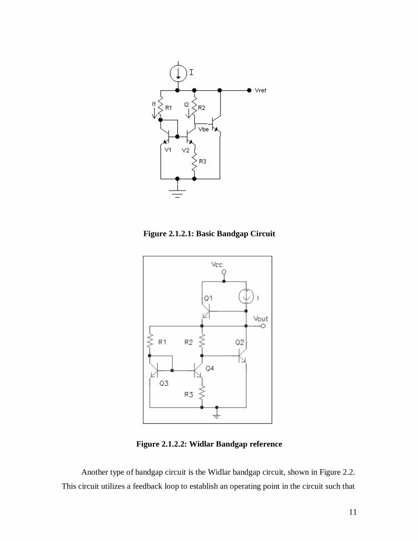
2.1.2 Bandgap References
The other popular form of voltage referencing is the bandgap reference. This
reference involves the creation of a voltage with a positive temperature coefficient. The
voltage is to have the same absolute value as a base-emitter voltage, VBE, with a negative
coefficient, so that when added together, the resulting voltage has a zero temperature
coefficient. The basic bandgap reference circuit starts with a current mirror with two
transistors operating at different emitter current densities (typically a ratio of 10:1). Iout,
which has a positive tempco, is converted into a voltage with a resistor and this voltage is
added to a normal VBE. The value of the resistor sets the amount of positive coefficient
voltage that can be added to the VBE. By choosing the appropriate impedance ratio, a
zero temperature coefficient can be obtained. This is achieved when the total voltage
equals roughly 1.23V. This value is the bandgap voltage of silicon. The interesting thing
about the bandgap circuit is that the constant current needed to run the circuit is actually
its own output current. Properly designed bandgap references compensate PTAT
(Proportional to Absolute Temperature) and CTAT (Complimentary to Absolute
Temperature) voltages to obtain a stable output. Other voltages may be obtained by
using this as the input to a precision amplifier with suitable gain.
11
Figure 2.1.2.1: Basic Bandgap Circuit
Figure 2.1.2.2: Widlar Bandgap reference
Another type of bandgap circuit is the Widlar bandgap circuit, shown in Figure 2.2.
This circuit utilizes a feedback loop to establish an operating point in the circuit such that

12
the output voltage is equal to a VBE (on) plus a voltage proportional to the difference of
two base-emitter voltages. If the transistor Q3 is turned off initially, transistor Q4 will
drive V1 in a positive direction. This will continue until the base of Q3 develops enough
voltage to produce a collector current equal to the value of I. This circuit will then
stabilize with voltage V2 equal to the base-emitter voltage of Q3. Once the circuit
becomes stable, the output voltage is
Vout = VBE(Q3) + VR2 (2.1.2.1)
where VR2 is
VR2 = (VR3)(R2/R3) (2.1.2.2)
The voltage drop across R3 is
VR3 = VBE(Q1) – VBE(Q2) (2.1.2.3)
The ratio of currents in Q1 and Q2 is set by the ratio of R2 to R1.
Bandgap reference circuits appear in many different configurations, but they all
operate under a specific format. These references involve the summation of a VBE with a
voltage generated by a pair of transistors, which operate under a certain current density
ratio. The goal of this project is to create a bandgap circuit, which creates a voltage
reference stable to 1% over a temperature range of -55° to 125°C. Why use a bandgap
and not a buried zener voltage reference? The zener or buried zener configurations will
not be used mainly because they are limited to a higher supply voltage than that of the
bandgap. With the bandgap reference, these limitations are not present.
2.2 Methods of Temperature Stabilization
Rudimentary methods of reducing the junction temperatures of transistors used in
the past have been eclipsed by superior design and fabrication techniques of today. For
example, regulators being manufactured today use low voltage supplies, such as +5V,
which means that the internal circuitry can be operated at high currents without excessive
dissipation.1 Also, large heat sinks are no longer required and the junction temperatures
can reach up to 150° Celsius before instability is an issue.
1 IEEE Journal of Solid-State Circuits, “New Developments in IC Voltage Regulators,” Robert Widlar,
Vol. SC-6, No.1, p. 2, February 1974.

13
2.2.1 Basic Bandgap Reference
The basic bandgap reference, or VBE reference, stabilizes its output by taking
advantage of the of a transistor’s temperature dependent parameters and characteristics.
Figure 2.2.1.1: Bandgap Reference Circuit
As previously mentioned, the temperature independent output voltage of the circuit
is a sum of two voltages: a positive temperature coefficient differential base-emitter
voltage of Q1 and Q2, and a negative temperature coefficient base-emitter voltage of Q3.2
33
2BEQBEOUT VV
R
RV +∆= (2.2.1.1)
Thus, it is theoretically possible to produce an output voltage that has a temperature
coefficient of zero by manipulating the ratio of R2 and R3.
An easy way to verify that the circuit is producing a zero temperature coefficient
output can be accomplished through looking at a derivation of Equation 4.
2
1030 ln
J
J
q
kTVV BEQg += (2.2.1.2)
where Vg0 is the bandgap voltage of silicon, VBEQ3 is the emitter-base voltage of Q3, and
the ratio J1/J2 is the quotient of current densities in Q1 and Q2. If the sum of the terms on
14
the right side of the equation equal 1.205V, Vg0, then it is clear that the output is
temperature invariant. While the nature of this circuit makes it difficult to produce
voltages above Vg0, having multiple stages of this circuit in a series string can attain
higher voltages.3
The above derivation ignores certain effects from base currents which arise from
production flaws which, in turn, cause variations in the gain, βF, and produce output drift.
These effects can be extreme when the current in Q2 is much too small to produce the
required deference in current density.4 Also, the derivation ignored two terms involving
the collector current because these terms are of the same magnitude as errors from non-
theoretical behavior and can be disregarded.5
The resistors used in the process for the above reference also deserves some
scrutiny since diffused resistors exhibit non-linearities as the temperature changes.6
Since an accurate reference depends heavily on the ratio of resistors R2 and R3, it is
imperative these issues become resolved. Layout techniques exist that counteract some
of the effects of temperature gradients, such as cross-quadding, but unfortunately, no
circuit design can eliminate these temperature effects completely.7
Using the bandgap circuit as a method of temperature stabilization is possible
because the emitter-base voltage is the most predictable parameter over a temperature
range and the differential voltage depends almost completely on the matching of the
transistors.8 The amplifier used in the reference circuits also use the same components,
namely resistors and transistors, such that the reference does not become a source of
noise, as does the zener reference.
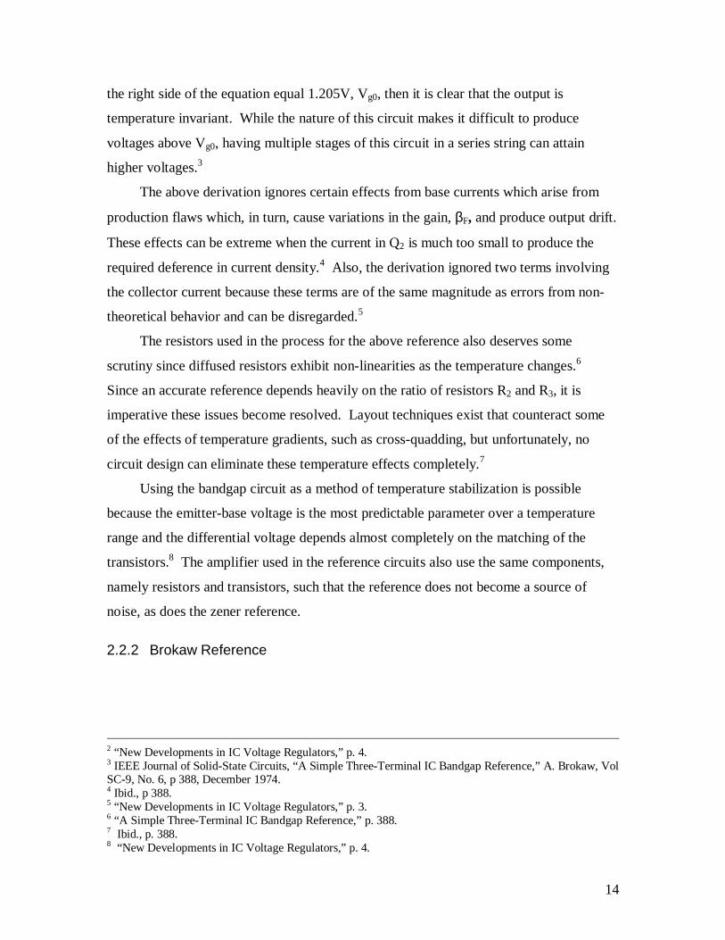
2.2.2 Brokaw Reference
2 “New Developments in IC Voltage Regulators,” p. 4.3 IEEE Journal of Solid-State Circuits, “A Simple Three-Terminal IC Bandgap Reference,” A. Brokaw, VolSC-9, No. 6, p 388, December 1974.4 Ibid., p 388.5 “New Developments in IC Voltage Regulators,” p. 3.6 “A Simple Three-Terminal IC Bandgap Reference,” p. 388.7 Ibid., p. 388.8 “New Developments in IC Voltage Regulators,” p. 4.
15
Brokaw improved on the basic bandgap reference by solving many of the
aforementioned problems. His design, shown below, has two transistors and collector
current sensing to establish the voltage reference.9
Figure 2.2.2.1: Brokaw Reference
This circuit eliminates gain variations, reduces difficulties involved with boosting
the output above 1.205V, and is able to use thin-film resistor technology. Through circuit
analysis, it is seen that the differential pair produces the same ∆VBE as in the basic
bandgap circuit and is directly proportional to the current density ratio and the absolute
temperature.
Also, the voltage across R1 is
2
1
2
11 ln2
J
J
q
kT
R
RV = (2.2.2.1)
since the currents through Q1 and Q2 are equal.10 This voltage has a negative temperature
coefficient assuming that the resistors and current ratios are uniform. Thus, the voltage
at the base of Q1 is the sum of VBE (of Q1) and V1 creating a temperature invariant circuit
as before.
9 “A Simple Three-Terminal IC Bandgap Reference,” p. 389.10 Ibid., p. 389.

16
2.2.2.1 Resistor Adjustments to the Brokaw Reference
Referring back to Figure 2.2.2.1, adjustments to the resistances R1 and R2 must be
considered as their temperature coefficients are not zero. If it is assumed that all changes
due to temperature fluctuations happens in R1, then it can be similarly assumed that any
voltage offset at the output is due to R1.11 However, the effect of the offset is reduced
since the output is a function of the ratio of R1/R2 but this does not change R1’s effect on
the current through Q1.12 Describing VBE as a function of the thermal voltage and the
ratio of Q1’s emitter current to its saturation current, and differentiating the result with
respect to temperature, leaves a reduction in the sensitivity, due to R1, of 47 times of the
original circuit.13 This reduction in sensitivity is still overshadowed by effects of the
diffused resistor’s temperature coefficients. However, when thin-film resistors are used,
an accuracy of 1 PPM per degree Celsius can be achieved.
11 Ibid., p. 393.12 Ibid., p. 393.13 Ibid., p. 389.

17
2.2.3 Curvature Correction
Usually the impedance ratios of the bandgap circuit can be manipulate to keep the
Figure 2.2.3.1: Curvature Correction
Vref curve within a desired range. Figure 2.2.3.1 shows how the parabolic shape of the
reference voltage can be shifted to stay inside the voltage range over a temperature drift.
However, sometimes curvature correction is necessary if the slope of the Vref curve
is too great. This section investigates the implementation of a precision CMOS bandgap
reference. This process embodies curvature compensation and differential offset
cancellation to achieve typical temperature drifts of 13.1 and 25.6 PPM/°C. In this
reference, a temperature-stable voltage is developed by adding linear and quadratic
temperature correction voltages to a forward-biased diode voltage, which is obtained
from the substrate p-n-p transistor available in CMOS processes. The linear temperature
correction voltage is proportional-to-the-absolute-temperature (PTAT) while the
quadratic temperature correction voltage is PTAT2. They are adjustable to set the
reference output voltage for a minimum temperature drift.
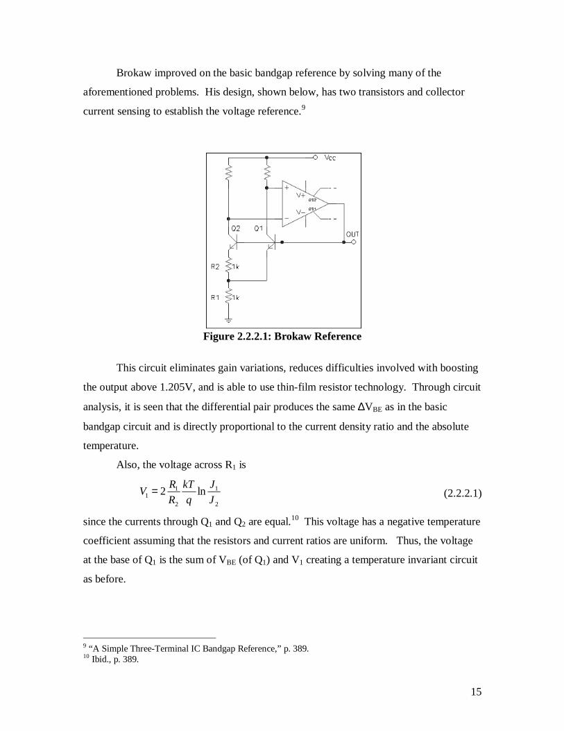
The overall concept of bandgap reference temperature compensation can be seen in
Figure 2.4. The first step is to add a PTAT correction voltage (KVT) to VBE to cancel out
the linear temperature variation of VBE. After the correction is added, the reference output
(VREF) will exhibit mostly the quadratic temperature variation as shown in the figure
below. A PTAT2 correction voltage (FVT2) can also be added to cancel out the quadratic
temperature variation of VBE. The final reference output should drift only due to higher
1.215
1.235
1.225
Vref
T °C
-55125
25
18
order temperature variations, and a zero tempco is achieved at TO, the temperature at
which the reference output temperature coefficient is zero. TO is also known as the
ambient temperature and is normally chosen to be near room temperature (25°C).
Figure 2.2.3.2: Curvature compensation concept
2.3 Methods of Adjusting and Trimming Resistors
The two types of resistors discussed in this section are thin-film, or hybrid, and thick-
film resistors. The reason being that these two types of resistors has the ability to be
trimmed to precise values. Trimming, for those who are unfamiliar to the term, is similar
to fine-tuning, or adjusting, the value of a component. First, selecting resistive material,
then removing the material until a predetermined value is achieved is one way to perform
this technique. Trimming is often needed due to uncertainties in the chemistry of IC
processing, which make it difficult to guarantee a precise resistor value. This is
especially the case with the design of voltage references, due to the importance of having
an absolute accuracy in order to produce a given output voltage. The resistance of thick-
film resistors can vary by as much as ±20 percent while thin-film resistors have a ±10
percent tolerance.
PTAT PTAT2
TO TO
T T
KVT FVT2
TO TO TOT T T
VBE VBE + KVT VBE + KVT + FVT2

19
Up-trimming is a means of increasing a resistor’s value by cutting into the resistor
and ultimately, reaching a selected value. Whereas, down-trimming through a method
called wire bonding, can jumper a section of the resistor. Of the two methods, up-
trimming is most commonly used. However, in all types of trimming, the resistor value
is constantly monitored as the material is being removed, ensuring that the required value
is reached at the right time and not over trimmed. There are also two basic ways of
trimming. The first, called static trimming, is a means of adjusting the resistor value
without power being applied. The second, dynamic or functional trimming consists of
adjusting a resistor to a specified value while the circuit is under power. Dynamic
trimming will be of importance to this study because the circuit will be powered while it
is being trimmed.
Depending on the methods used to trim, thin-film resistors can be trimmed to ±0.1
percent of value and thick-film resistors to ±1.0 percent. Also, when trimming thin-film
resistors, special care and controls are necessary to avoid too much penetration into the
dielectric area of the resistive material. However, the application of thick-film resistors is
suitable only for printed circuit board environments due to the process of applying the
resistive material and the size of the resistor. Also, the use of thin-film resistors proves to
be more beneficial because higher accuracy can be obtained when up-trimming.
2.3.1 Abrasive Trimming
Abrasive trimming is the first manner to be used in resistor trimming. Laser
trimming has far replaced this technique, but for use of background references and
comparisons, this technique will be discussed. In abrasive trimming, fine-grained sand is
forced through a small nozzle under high air pressure. This is why this technique is
sometimes called air-abrasive trimming. The sand wears away and removes resistor
material until the desired value is obtained. The process of removing resistor material is
done in one of two ways, by forming a kerf or cut, as does a laser and by reducing the
thickness of the resistor film. Reducing the film thickness increases the sheet resistivity,
and thus changing the value. Abrasive trimming does produce more stable resistors
because heat is not involved in the process, but still suffers in many areas. The process is
slow and produces large cuts due to the fact that the size of the any air-abrasive nozzle is
20
far greater than that of a laser beam. And even though abrasive trimming has cost
benefits in terms of setup and capital costs, the process is dirty and even dangerous.
Particles being shot out of an air-abrasive nozzle at high speed bounce off the resistor
being trimmed and often end up acting as destructive projectiles.
Table 2.3.1.1: Advantages and Limitations of Abrasive Trimming
Pro’s Con’s
Ease of setup Slow process
Low capital costs Dirty process
Produce stable resistors Produces large kerf
Low noise for high value resistors
2.3.2 Laser Trimming
Laser trimming started off in the early sixties and has developed from a process
that “offered a lot of promise” to a solid reality. It has definite advantages that make it
the trimming method of choice for both thin-film and thick-film resistors. There are two
widely used laser systems: (1) A neodymium-doped yttrium aluminum garnet (YAG)
crystal laser, (2) A carbon dioxide (CO2) laser. Some resources state the YAG laser
beam is better because it has a shorter infrared wavelength of 1.06 µ (microns), which
permits smaller, narrower cuts and minimizes damage to the resistive material as well as
to the underlying dielectric. But a case is made for the CO2 laser to be used with thick-
film resistors. The advantage here is that the focal length limitations are smaller and a
CO2 laser can trim warped substrates. It should also be noted that the YAG laser beam is
invisible, and trim schemes using a YAG laser also incorporates a helium-neon (He-Ne)
laser that is collinear with the YAG. This laser gives off a red beam that shows the
position of the YAG beam. A He-Ne laser is also needed when using CO2 lasers, which
typically operate at 10.6µ.
In laser trimming a beam is shaped and focused on the plane of the resistor, through
a series of mirrors and lenses. The laser beam then hits the resistor material, energy is
absorbed, and the material heats up and vaporizes. The beam can be moved in an X or Y

21
direction by manipulating the mirrors to produce a desired cut. Thus, the ease of
movement of the beam is a certain advantage over conventional methods and allows for
several different resistors to be trimmed in one setup. A list of laser trimming terms, in
Appendix A, is provided in order to assist those unfamiliar with the terms used in this
section.
Laser cuts are created by a series of short physically overlapping pulses, typically
100 µsec and 0.001 inches in diameter. Laser parameters are usually set to be short
pulses and at a high peak power, in order to eliminate problems such as thermal shock
and microcracking in the resistor’s material. Thereby, the amount of heat flow into the
bordering regions is also reduced.
The laser trim process is completely automated. And despite its stop-and-go style,
can trim at a rate of several inches per second. The laser beam and the X-Y table is
controlled by a computer, and laser stations are typically setup with a TV camera to
monitor the trim process. A laser trim station, basically, operates as follows:
1) The resistor is examined.
2) A digital voltmeter (DVM) measures the resistor value.
3) The laser is positioned at the start of the trim. This point is programmed into the
computer.
4) The laser pulses and cuts away at the resistor’s material
5) The DVM takes another reading.
6) The computer compares the reading with the required reading and either shuts off the
pulsing, if the value is within tolerance, or it pulses the laser again.
7) This process continues until the resistor value is within the specified tolerance.
Figure 2.3.2.1, on the next page, shows the difference between a laser pulse with a
small bite size verses one with a large bite size. The time it takes to complete a trim
varies based on the number of pulses and the size of the bite. However, Figure 2.3.2.1
illustrates that in order to produce a clean laser cut without a ragged kerf, the bite size
must be small and therefore will take more time to trim.
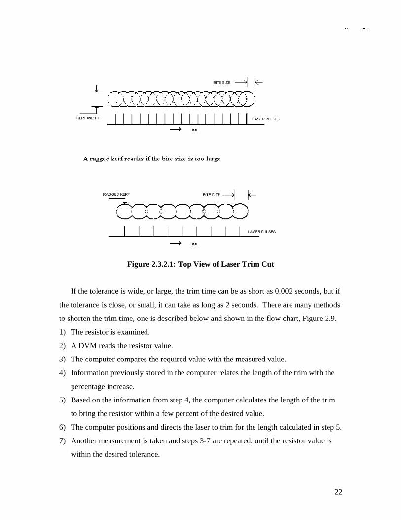
22
Figure 2.3.2.1: Top View of Laser Trim Cut
If the tolerance is wide, or large, the trim time can be as short as 0.002 seconds, but if
the tolerance is close, or small, it can take as long as 2 seconds. There are many methods
to shorten the trim time, one is described below and shown in the flow chart, Figure 2.9.
1) The resistor is examined.
2) A DVM reads the resistor value.
3) The computer compares the required value with the measured value.
4) Information previously stored in the computer relates the length of the trim with the
percentage increase.
5) Based on the information from step 4, the computer calculates the length of the trim
to bring the resistor within a few percent of the desired value.
6) The computer positions and directs the laser to trim for the length calculated in step 5.
7) Another measurement is taken and steps 3-7 are repeated, until the resistor value is
within the desired tolerance.

23
This technique requires fewer measurement and laser stops, which results in a faster
trim time. It should be noted that typically, increasing the complexity of the process
involves more complex software and thereby making the process more expensive. But if
a large quantity of resistors is to be produced, software complexity and cost becomes
small compared to the savings brought about by a faster throughput. The following
figures are flow charts of the basic laser trim system and the faster method described
above.
READ VALUE
SCRAP
PULSE THELASER
COMPARE WITHREQUIRED
VALUE
GO TO NEXTRESISTOR
Figure 2.8: Flow chart for basic lasert r im method us ing feedback
TRIM TOCALCULATED
LENGTH
CALCULATELENGTH OF
TRIM NEEDED
COMPAREWITH
REQUIREDVALUE
READVALUE
ENDPROCESS
Figure 2.9: Flow chart for faster tr immethod ut l i l iz ing calculat ions and feedback
HIGHWITHIN
TOLERANCE
LOW
WITHIN TOLERANCES

24
Laser trimming, as previously discussed, has clear advantages over abrasive trimming,
but is by no means a panacea. A list of advantages and limitations of laser trimming
follows in Table 2.3.2.1.
Table 2.3.2.1: Advantages and Limitations of Laser TrimmingPro’s Con’s
High speed Intense heat at trim area – causes microcracks
Permits data logging Cracks cause noise in high value resistors (over 5 MΩ)
Automated Large capital investment
Highly accurate Requires software development
Clean
To conclude this section, a list and definition of different types of resistor trims as
well as physical drawings are provided for each method. Shown in Figure 2.10, are
various types of trims but the most popular are the plunge cut, L-cut, scan cut, and
serpentine cut.
Plunge Cut: A fast cut that is usually used on resistors of one square or less.
Disadvantages include the most disturbance of current through the resistor and the cause
of a hot spot to form at the top of the trim.
Double Plunge Cut: Allows a coarse trim followed by a fine trim. Laser damage is less
then the L-cut, but this cut can cause an even bigger hot spot than the single plunge cut.
L-Cut: Provides more accuracy than the plunge cut. The perpendicular leg provides a
coarse trim, while the parallel leg provides a fine adjust. The angular and J-Cut are more
stable and provide fewer hot spots then the L-Cut. This is due to the removal of any
sharp turns in the trim.
Scan Cut: The slowest but the most stable and accurate. It does not disturb the current
flow as much as the other trims. Best for high frequency applications. They result in low
thermal noise because no hot spots are formed in the resistor.
Serpentine Cut: Usually used when a large resistance change is needed when increasing
the current path length. Must be used on large area resistor designs.

25
Figure 2.3.2.4: Types of cuts for resistor trimming
2.3.3 Link Fuse Trimming
Link fuse trimming is a process of selecting a desired resistance from a series of
geometrically increasing resistors fused together by thin jumper wires. Connected to
each end of a fuse are two probe pads, approximately 100µ per side. Through these
probe pads, a current, in the order of mA, is applied to selected fuses and in doing so,
blows open the fuse. However, these probe pads are extremely large when compared to
the size of the resistor on an IC. Plus, for every resistor (R1, 2R1, 4R1, …, 2(n-1)R1) that
is used in the series, (n + 1) probe pads are needed to trim the circuit needed and, thus,
take up even more room on an IC. For each resistor that is used in the series, designers
have a wider resolution and are able to select a higher precision resistor between the two
terminals. Therefore, with precision directly related to the number of resistors in series, it
becomes clear that, in order to achieve precise resistor values, more area is needed on the
IC. This poses a problem in that the designer must choose which is of greater
importance, area consumed on the IC or precision. Nevertheless, this process can be a
simple one and is currently implemented at Allegro. Also, link fuse trimming can be

26
programmed easily and the process is fast compared to the other methods of trimming
previously discussed.
There are two types of resistors that are used when link trimming. Metal resistors
typically have a sheet resistance of 0.07 Ω/ (ohms per square) while typical polysilicon
resistors have a sheet resistance of 23.1 Ω/. Because metal resistors have such a low
sheet resistance, the designer could use the resistor as the fuse, whereupon blowing the
fuse would result in an open circuit. Another advantage of metal resistors is that really
low values can be obtained because of their sheet resistance of 0.07Ω/. However,
using metal resistors requires an extra step to added to the fabrication process and is not
worth using, especially since high currents are not needed to blow the links in the
intended design. This is why polysilicon resistors should be used when link fuse
trimming. Figure 2.11 below shows a graphical representation of a typical link fuse trim
system.
Figure 2.3.3.1: Process of Link Fuse Trimming
Also, Table 2.3.3.1 lists the advantages and disadvantages of this process.
Table 2.3.3.1: Advantages and Limitations of Link Fuse TrimmingPro’s Con’s
No initial investment Takes up more space on IC
Easily programmable Less precise due to inaccurate components
Simple process if silicon is used Complex process if metal is used
Fast

27
2.3.4 Circuit Adjusting with Potentiometers
In the past, the multi-turn trimming potentiometer has been the traditional tool used
for adjusting a resistance within a circuit. A multi-turn potentiometer, or trimpot, is an
electromechanical device that usually has a shaft that is turned to set its resistance or
voltage division ratio. The shaft is usually adjusted with a screwdriver and the output of
the circuit is viewed on an instrument. When the output is at its desired level, the
operator applies a drop of paint or glue to fix the shaft’s position. This concept is a
simple one and also inexpensive. Prices for trimpots range from $0.25 to as high as
$1.00 for one trimpot. However, price does decrease as the volume bought increases.
Nevertheless, automating the process is costly and difficult, and in order to trim precise
values skilled workers must be used.
2.3.5 Using Zener Diode Sets for Adjustments
Also referred to as “Zener zapping”, adjusting circuit components with the use of
zener diode sets and resistor sets is also an option. Zener diode sets and resistor sets are
fused together with jumper wires to cut unwanted elements out of a circuit and thereby
select a voltage drop. However, precision accuracy poses a problem when using zener
diode sets.
2.3.6 Electronically Programmable Analog Devices
The company, Advanced Linear Devices Inc. (ALD), has made available the
technology to adjust and trim circuits using a solid state device. This invention, called an
electronically programmable analog device (Epad), functions just like a trimpot but with
electronic precision instead of mechanical. An Epad is a CMOS integrated circuit that
uses computer control to electronically program threshold voltages that can be accurately
controlled via stored charges. Changing the threshold turn-on voltage of a MOSFET, for
a given input, in turn changes its drain on-current. By altering the drain on-current, the
on-resistance can then be set and controlled. Using a computer (IBM compatible with
386 processor or higher), an Epad programmer, and control software can control these
threshold voltages.
This CMOS IC consists of a floating-gate MOSFET that once programmed, will
inject “hot” electrons that have enough energy to leap from the channel over its energy

28
barrier into the oxide and onto the floating gate. This floating gate is made up of a layer
of polysilicon embedded in the layers of oxide bridging the control gate and the channel
of the transistor. Once in the floating gate, the electrons are trapped and indefinitely
retained. Even when power is removed, the charge remains, this is called nonvolatile
electron charge storage.
Epads come on a single silicon chip that contain two or four devices. Each device
is a trimmer whose threshold voltage can be programmed by a series of voltage pulses.
These pulses are rapidly delivered until the required threshold voltage is obtained. These
devices can be programmed and configured in many different ways depending on the
application needed.
To use Epads, one must load a specific software product that ALD offers, onto a
PC that will be used as an interface between the user and the programmer. The
programmer, which is a customized device sold by ALD, is setup to an adapter, which is
also an ALD product. The adapter is then connected to the Epad that can be used in a
variety of applications. If necessary or desired, the user can create a program that will
interact with the customized ALD software and the PC. Once software is loaded and the
system set up, adjusting a circuit is just a matter of inputting a variety of values into the
PC based program. These values include, the threshold voltage, a baseline voltage
threshold, and resolution parameters and each of these values are entered into one of two
windows that appear on the PC screen. Programming is then activated with a push of a
button, whereupon, a series of pulses begin, and continue until the required threshold
voltage is reached. The process is completed within seconds, the actual time depending
U S E RP R O G R A M
C U S T O M I Z E DC O N T R O L
S O F T W A R EP C
P R O G R A M M E RI N T E R F A C E
A D A P T E RE P A D &
A P P L I C A T I O N
Figure 2.12: Epad Process Flow

29
on the application. Figure 2.12 shows this flow of processes for a basic model.
Disadvantages of Epad trimming is as follows:
• The threshold voltage will vary slightly with temperature.
− A crossover point, a point where the threshold voltage is very stable, is68µA
• Epads are subject to voltage relaxation, where stored electrons, particularly the oneslocated near the oxide-silicon interface, gain enough energy to escape the barrierholding them in.
− Typically the threshold voltage drops about 0.3 percent and stabilizes 6hours after programming. However, this can be compensated for, byprogramming a higher initial threshold voltage.
• Epads are sensitive to electrostatic discharge (ESD) and proper precautions need to be
taken.
Final notes to consider:
• Epads are intended for use in low voltage micro-power circuits where the operatingvoltage should never exceed 10V.
• All Epad products are registered ALD products and all costs refer to ALD price lists.• Epad chips are available for commercial (0 to 70 °C) and military (-55 to +155 °C)
applications.• Available in dual 8 pin packaging and in quad chips with 16 pins.• Prices start at less then a dollar for either unit bought in high volume.
− One quad chip costs $2.62 and one dual chip costs $2.10• Price of programmer (E100 Programmer) - $499.• Adapter module prices vary from $149 - $199.• Typical drift is less than 2mV in 10 years.
2.3.7 Comparison of Different Trimming Techniques
To conclude this section, a comparison will be made of the different methods of
trimming and adjusting and then a method, or methods, will be recommended that will be
most beneficial. To compare these methods a metric was formed. To start off this
analysis, air abrasive trimming and potentiometers were eliminated because these are the
two oldest forms of resistor trimming and both are far inferior to the other four trim
methods discussed. Therefore, in this metric the comparison will include laser trimming,
link fuse trimming, Epads, and zener diode sets. In this metric each method of trimming
is compared in different categories and are ranked, in order, from excellent to very poor.

30
When ranking each method a number from 1 to 4 will be assigned, where the number 1
will represent the best method and the number 4 will represent the worst method.
Table 2.3.7.1: Rank System for MetricRank Representation
1 Excellent
2 Good
3 Poor
4 Very Poor
A ranking metric, in general, can often be confusing and misleading because the
difference between one comparison and another can be much larger than the given rank
shows. This comparison metric will show two different methods to have the same rank
when the comparison between the two is different but still close enough to negate any
major advantage. The number is placed in bold font if this factor proves to be a major
disadvantage or advantage for the method being examined.
Categories covered in this metric will be cost vs. time to trim, cost vs. area used in the
IC, and cost vs. total investments to be made. Other areas to be examined include
accuracy and simplicity and therefore will also be entered into the metric. These
different factors will also be ranked in order of importance so some categories will
outweigh others. In Table 2.3.7.2, the time column represents the time it takes to trim
one component. The column labeled area consumed refers to how much chip area this
trimming technique will take up on the actual IC. Finally, the column labeled total cost
refers to the combination of an initial cost and a price per unit trimmed. Initial costs refer
to all costs that are spent before any trimming actually takes place, and can also be
considered non-recoverable engineering costs. Whereas, price per unit trimmed shows
how much money will be needed to trim one unit, based on a certain volume of
components being trimmed.
Based on these guidelines, the following metric was formed, which shows major
advantages in choosing laser trimming and link fuse trimming when compared to the
other methods of trimming. A note to be made regarding laser trimming is that total cost

31
decreases as the volume produced becomes larger. Therefore, if the anticipated volume
were extremely large compared to the initial price, then laser trimming would be the
method of choice for this project.
Table 2.3.7.2: Comparison metric for resistor trimmingType of
Trimming
Total Cost Area
Consumed
Accuracy Simplicity
of Process
Time to Trim
Laser 3 1 1 1 2
Link Fuse 1 3 3 2 1
Epad 3 4 2 - 1
Zener Zapping 2 2 4 2 1
In this metric, it is shown that Epads and zener diode sets can be useful methods of
trimming, but for this process they should be considered of lower rank to laser and link
fuse trimming. For zener diode sets, the combination of area used on the chip and poorer
initial accuracy eliminates this method from a high recommendation. As for Epad
technology, the idea and concept seems to be easily incorporated, but the fact that an
extra IC eliminates the option of buying and utilizing this product. However, there is one
option that can be suggested if this technology is requested. ALD, the creator of Epad
technology, could be contacted with an offer to purchase the rights to the patented design
and combine their design within the new bandgap reference design. In doing this, a
certain amount of money would have to be paid to ALD whenever their design is used.
This can be costly if plans are made to mass-produce the bandgap reference. It would
also require a more complex design than is necessary to complete this task, but still
remains an option to be considered.
From this comparison, laser trimming appears to be too expensive a process to
recommend at this time. Link fuse trimming on the other hand, provides benefits due to
the fact that this process is currently being implemented at Allegro, rendering the initial
and total prices to be low. But laser trimming provides many more advantages, such as
less area consumed on the IC, high accuracy, as well as a simpler process. Whereas, link
fuse trimming requires the use of large probe pads that take up much space on the IC,

32
making this process unattractive to IC design. For these reasons, it was decided to use
another option, to combine both laser trimming and link fuse trimming, therefore
achieving the benefits of both methods and eliminating some of the disadvantages. This
process would use link fuse trimming but with a laser in place of two probe pads breaking
the fuse between the resistor pairs with current. This would also speed up the trimming
process considerably, making this method appealing.
To conclude this analysis, the techniques shown below, in order of preference, are
the methods of recommended trimming:
1. Combining link fuse and laser trimming techniques in one technique2. Applying a full laser system for circuit trimming to the design process3. Utilize the current process of link fuse trimming4. Obtain the rights to ALD’s Epad technology and implement it in the new deisngn5. Using zener diode sets as a method of trimming resistor values

33
3 Methodology
Being able to design an accurate voltage reference and ensuring the output
remains constant over temperature is the fundamental problem of this project. A project
of this magnitude requires a carefully planned approach in order to accomplish all the
required objectives. This chapter serves as a procedural guide as to how this project will
be completed in the terms to come. Developing an accurate voltage reference relies on
many factors that involve the development of an accurate specification sheet, the design
of our own integrated circuit, and testing that procures favorable results. The goals of
this project include determining the best type of voltage reference for this project,
utilization of trimming to obtain accuracy over temperature, and, ultimately, designing an
IC that will be used by Allegro Microsystems. Specifically, it is suggested to involve the
bandgap voltage reference for our design and link fuse trimming as our form of adjusting
the IC’s components.
3.1 Developing a Background
In determining the specific type of voltage reference we will be using, we looked
into two different theories. The first technique involves the destruction of zener diode
junctions and the second entails the implementation of the bandgap principle. After
determining the bandgap reference had significant advantages over the zener reference,
we chose to further investigate the usage of bandgap voltage references. We researched
BJT temperature behaviors to better understand how our circuit will respond to ambient
temperature variations. Also, we investigated various bandgap voltage references that
other designers have made in order to develop our own specification sheet.
Through more background research, we saw there was going to be a need for
some form of circuit or resistor trimming in our design. After examining many different
methods of trimming, we were able to form a metric that helped determine the most
efficient process to use for trimming IC's and for our project. We concluded that laser
trimming would be the most efficient and cost effective means of trimming IC's if mass
quantities of IC's needed to be trimmed. However, for our project with only fifteen
circuits to trim, we decided that link fuse trimming would be the best method for us and

34
made recommendations to incorporate this process. Next, after our background research
is completed we will be able to put together a specification sheet that will be used as a
reference when designing our circuit.
3.2 Design of the Integrated Circuit
The next stage of this project will include the design of our IC. With a solid
background, we can now begin to create our own design. Design of the circuit involves
the use of Computer Aided Design (CAD) software, such as L-Edit or Cadence Virtuoso,
which allows the user to design every transistor, resistor, and capacitor individually and
tailor each component to meet specific needs and specifications. The process is quite
detailed and is the most critical part of the whole procedure. While some flaws can be
compensated for after fabrication, fundamental design errors can not be reversed.
3.2.1 Desired Specifications
Every design must have some specifications that the designer must meet. The
specifications for our voltage reference are shown below in Table 3.2.1.1.
Table 3.2.1.1: Desired Specification SheetMin. Typ. Max. Units
Output Voltage 1.238 1.250 1.262 V
Maximum Tempco - - 40 ppm/°C
Initial Accuracy - - ±5 mV
Supply Voltage 3 5 5 V
Temperature Operating
Range
-55 - +125 °C
3.2.2 Choosing a Design Model (Brokaw vs. Widlar)
Once the decision was made to use a bandgap reference, there became another
choice of which model to follow Brokaw or Widlar. As stated in Chapter 2, the Widlar
bandgap reference is a basic reference circuit with many flaws that will probably be
encountered throughout the design phase. Such flaws are:

35
• Current is derived from the power supply and may vary with power supplyvariations
• Variations in the gain• Output drift
The Brokaw model was chosen because it eliminates these problems and can be used
with trimmable thin film resistors so that a higher grade of accuracy could be obtained.
3.2.3 Choosing Design Layout Tools
To design the layout of our circuits, we had to choose a software package that
would be both easy to learn and simple to use yet provide advanced features such as
circuit and layout simulation. The options were limited to using either Tanner Research's
L-Edit layout program or the Virtuoso family of tools from Cadence Design.
Tanner's L-Edit was found to be clunky, or full of 'bugs', and had a seemingly
slow learning curve. To simulate our extracted layout, we would need to use an external
SPICE simulator.
The choice was then clear to use the Cadence tools for several reasons. The
Cadence tools included several other programs that made design verification simple
through schematic entry and simulation. Simulation of our circuit and extracted layout
were done using Analog Artist, a front-end simulator for SPICE, which was included in
the Cadence software suite. Also included in the package was an advanced Layout
Versus Schematic (LVS) checker that highlighted the differences between our layout and
our intended circuit configuration. Due to the automation of some tasks in Cadence, such
as copying multiple instances or generating the layout of a MOS transistor, the program
was easier to learn. We also chose the Cadence tools because we already had experience
using Tanner tools and we wanted to expand our knowledge and our experience by
learning another CAD tool.
3.2.4 Choosing a Fabrication Process
Before designing a layout, a fabrication process needed to be chosen. The process
chosen would set the design rules used, the minimum feature size, the operating voltage
of the circuit, as well as the number of poly and metal layers available. It was desired to
have two poly and two metal layers to ease in the routing of signals throughout the
circuit. In addition, smaller feature sizes allow more transistors to be fabricated in a

36
smaller area. The ability to manufacture true NPN bipolar transistors was also a
necessity since correct operation of our circuit depended on a base-emitter voltage of a
bipolar transistor. However, the availability of a NPN option was not critical in the
decision to choose a process because PNP transistors could still be made in either process
using the p-type bulk.
The foundry of choice, the MOS Implementation Service (MOSIS) from
California, provided two processes that would be suitable for the fabrication of our
circuit: a 2.0µ 2-metal, 2-poly, NPN, 5V supply process from Supertex, Inc and a 1.2µ 2-
metal, 2-poly, NPN, 5V supply process from AMI. Since both processes had many of the
same features, either process could have been used. However, when examining the
fabrication schedule, it was noticed that the AMI process runs correlated with the WPI
academic schedule and that a run would be done at the end of the fall semester. This
scheduling of the process runs, along with a smaller feature size, prompted us to use the
AMI 1.2µ process.
3.2.5 Trimming Technique
As stated earlier in the second chapter, the process of link fuse trimming will be used
in order to achieve our goal for initial accuracy. To recap, the reason link fuse trimming
will be used is mainly due to laboratory equipment restraints, the only means of trimming
an IC we have access to is a probe station, which can be used to cut links. Other reasons
include insufficient funding for laser trimming equipment, research purposes, and
Allegro, our sponsors, currently use link fuse trimming. For all these reasons, we chose
the process of link fuse trimming.
In order to prepare for designing a link fused-trimmable resistor, other restraints
had to be considered. We had to make sure our fabrication process would provide the
necessary tools to layout all the components of this trimmable resistor. One example is a
probe pad that is typically a square of metal, which can be accessed by placing a glass
opening over the metal square. This probe pad is one component in the link fuse process
that we need to be able to layout and have our fabrication process be able to handle.
After evaluating the AMI process, we concluded our trim resistor would consist of
metal2-probe pads with a glass opening, metal2 fuses, and poly resistors. This process

37
provides us with all the necessary criteria to stay within our limits of a two-metal, two-
poly process.
3.3 Simulating and Testing Our Design
Upon completion of our initial design, we will use PSpice to simulate our circuit
to see if any problems ensue from our design. Two types of problems can arise after the
simulation of a design. The first is an error in the actual design of the circuit. Any
connections not made, unassigned variables, or values that are incorrectly entered will be
flagged immediately.
Once the design is free of error, design and simulation can begin using Cadence to
provide a more accurate portrayal of our circuit than PSpice could. Using Cadence, we
can layout our components from our schematic and ultimately run a LVS to verify that
our layout is accurately represents our circuitry. Once our design has been verified, any
type of simulation or graph can be produced and recorded.
This is where the second form of error can occur. If the simulation results are not
as expected and show that changes in our design are required to meet specifications, then
the appropriate alterations will be made. As previously stated, editing a PSpice
schematic or Cadence design is a fairly simple process if one is familiar with the
programs. Components can be added and connections made by clicking and dragging on
the screen. Double clicking on a component or connection and typing in relevant
information will allow the user to input values and names into the program. Parametric
tests will be performed during simulations to ensure that our design will operate within
the specifications stated. These tests will be clearly defined later in this project using an
organized test procedure and trim procedure so the user can follow the correct steps
necessary to test and trim our bandgap circuit.
3.4 Completion of the Project
The last part of our project will conclude our final analyses, conclusions, and
contain all our findings from the previous sections. It will contain our results from
PSpice testing and the Cadence revisions. We will report our conclusions on the
feasibility study, which will ultimately be based on the actual success of this project.
This area of the project will not only be dedicated to our results and conclusions, but will

38
include recommendations regarding any future studies that can be looked into as a result
of our project.

39
4 Design
The circuit is modeled after the Brokaw's Cell and is shown in Figure 4.1
Figure 4.1: Schematic of the Bandgap Voltage Reference
Several different designs were simulated before deciding on which design to employ
and build upon. This design incorporates a pair of diode connected bipolar junction
transistors (BJT) which are difficult to realize in a CMOS process. The final design also
includes transistors that act as current sources for the two branches in the circuit. There
are also three resistors in the circuit: two fixed value poly resistors and one trimmable
poly resistor that can be trimmed via link fuse trimming. Providing negative feedback in
this circuit is an operation amplifier designed to produce a high gain and low offset
voltage.
The above components were designed to produce a 1.25-volt output that was then
used as the input to an op-amp with a non-inverting gain of two. Two PMOS transistors,
designed to behave as resistors, supplied the correct amount of feedback to the amplifier.
The value of 2.50 volts was chosen as an initial specification because most bandgap
circuits on the market today are designed for 2.50 volts. The final product includes the

40
design of a 1.25 volt reference that is amplified to 2.50 volts, where both references are
considered outputs and can be used together or individually.
4.1 The Brokaw Cell and the Bandgap Voltage
The output of the Brokaw cell is a function of two voltages: one that is proportional
to temperature (PTAT) and one that is complementary to temperature (CTAT).
Looking at Figure 4.1, the base-emitter voltage of Q1 can be seen at the non-
inverting terminal of the amplifier. Through the principle of virtual ground in a negative
feedback amplifier, the voltage at the non-inverting node appears at the inverting node.
Thus, the voltage difference between the two base-emitter voltages, ∆VBE, will appear
across resistor R2. Also, the current through R2 can be expressed as ∆VBE/R2.
Since no current can flow into an input terminal of an amplifier, the current
through R2 must also flow through resistor Rt. The voltage drop across Rt can then be
expressed as:
tBE
R RR
VV
t
2
∆= (4.1.1)
The bandgap output voltage is then a function of the base-emitter voltage VBE1 and the
drop across Rt, or
tBE
BEBANDGAP RR
VVV
21
∆+= (4.1.2)
The CTAT voltage in this relationship is easily seen but the PTAT voltage is hidden
deeper.
Looking more closely at the ∆VBE term, it is seen that this term is the difference
between two base-emitter voltages. Through manipulation of the equation for the
collector current of a transistor, VBE equals:
S
CtBE
I
InVV ln= (4.1.3)
Also, by substituting this expression into the equation for ∆VBE, it is seen that
−
=∆
2
2
1
1 lnlnS
Ct
S
CtBE
I
InV
I
InVV (4.1.4)

41
The term nVt is common to each expression and due to matching, should not vary
from one transistor to another. Factoring out nVt then leaves the difference of two natural
logarithm functions. By simplifying the natural log expressions, it is then seen that
=∆
1
2
2
1lnS
S
C
CtBE I
I
I
InVV (4.1.5)
It is seen now that ∆VBE is directly proportional to the thermal voltage that is
directly proportional to temperature itself and that the output is a direct function of two
voltages, one CTAT and one PTAT.
Now that the equation for the bandgap output voltage has been derived, further
simplifications can be made. It has been previously established that the voltages at each
terminal of the amplifier are equal. Thus, it is indisputable that the voltage across the
resistor R1 is equal to the voltage across Rt. So if,
RtR VV =1 (4.1.6)
then it is permissible to say that
tCC RIRI 211 = (4.1.7)
Then the ratio of IC1 to IC2 is equal to the ratio of Rt to R1. Substituting the resistor ratio
Rt/R1 into the expression for ∆VBE results in
=∆
1
2
1
lnS
SttBE I
I
R
RnVV (4.1.8)
Then the new equation for the bandgap output voltage is given as
+=
21
2
11 ln
R
R
I
I
R
RnVVV t
S
SttBEBANDGAP (4.1.9)
This new equation expresses the output voltage not only as a function of CTAT and
PTAT voltages, but also as a ratio of the resistances Rt, R1, and, R2.
4.2 AMI 1.2µ Process
As previously mentioned, the AMI ABN process, a low noise analog CMOS
process offered through MOSIS, provides two polysilicon layers and two metal layers
and a special p-base layer to create true NPN bipolar transistors. The process was rated
to operate up to 5V and across the temperature range of –55°C to 125°C.
42
The smallest available die size was a 2.20mm by 2.20mme "TinyChip" that was
packaged in a standard ceramic 40-pin DIP package with a lid taped on that was easily
removed.
While the minimum feature size of this process was 1.2 microns, MOSIS made
the suggestion that if the design included analog signals, the minimum gate length for a
MOSFET should be at least 1.8µ because the ABN process was a scaled version of
another AMI process. From previous runs, it was learned that a 1.8µ gate length better
preserved the intended analog signal transmission. For digital signals, however, a 1.2µ
gate size was acceptable.
4.3 BJT Models
The Brokaw cell required a complementary to absolute temperature voltage, which
was gained by creating a stand-alone base-emitter voltage of a bipolar transistor.
4.3.1 Diode Connected Transistors
To gain access to a base-emitter voltage, a bipolar transistor was diode-connected
such that the three-terminal device becomes a two-terminal device by shorting the base to
the collector thereby making it appear as only a diode.
A diode-connected transistor was used instead of a simple diode because of the
constant n that appears in the equation for the collector current:
tnVbeV
eII SC = (4.3.1.1)
For diodes, the constant n is can vary between 1 and 2 (depending on the physical
structure and material used) whereas for transistors, n is usually 1. For transistors
operated at relatively high or low currents, n approaches 2. The transistors in this circuit
will only see approximately 100µA of current and, therefore, n should stay around 1.
Also, the I-V characteristic of a diode-connected transistor remains the same as the IC-
VBE characteristic since the transistor is still being operated in the active region (VCB=0V,
VBE>0.7V).

43
4.3.2 NPN Transistors in a CMOS Process
A NPN transistor consists of two pn junctions that are connected back to back.
Usually, it is not possible to fabricate a bipolar transistor in a CMOS process, but the
AMI ABN process provided a special p-type base layer that would serve as the base of
the transistor. The NPN transistor was designed according to recommended
specifications from the MOSIS home page.
Figure 4.3.2.1 shows how impurities will be diffused into the silicon to create a
NPN transistor.
Figure 4.3.2.1: Cross-section of a NPN transistor in CMOS Process
The collector is an n-well set in the p-type substrate. The base layer, as
mentioned before, sits in the n-well, and the n-active emitter is diffused into the base
layer. The current flows vertically through this transistor if the base and emitter are
appropriately sized according to the MOSIS recommendations.
The layout of the transistor was done in Cadence and can be seen in Figure
4.3.2.2.

44
Figure 4.3.2.2: Layout of NPN Transistor
The dark green, orange, and lime green areas represent the n-well collector, p-type base
layer and the n-active emitter respectively. The blue is Metal-1 and can be seen
connecting the collector to the base. To reduce contact resistance and distribute signals
evenly, multiple contacts in the form of a ring were used to connect layers. A single
diode-connected NPN transistor measured 57.60µ by 52.50µ with an emitter area of
83.25µ2.
4.3.3 PNP Transistor in a CMOS Process
A PNP bipolar transistor is constructed much like a NPN transistor except the
layers are diffused differently. AMI did not provide a special base layer for a PNP
transistor and, thus, makes it impossible to make a true PNP transistor in this process.
However, by taking advantage of the layers of the CMOS process, a device that acts like
a PNP transistor can be made. Figure 4.3.3.1 shows the layers of this device.
The emitter is made using a p-active diffused area set in an n-well base. The n-well
sits in the p-type substrate that acts as the collector. It is important to note that because
the substrate is being used as the collector, and that the substrate will be connected to

45
ground, the collector is also automatically tied to ground. The current flow in this device
is both vertical and lateral depending on sizing considerations of the base and emitter
areas. There were no recommendations from MOSIS or AMI on how to size this device
since it is not a supported or suggested option in this CMOS process.
Figure 4.3.3.1: Cross-section of a PNP device in CMOS Process
The layout of the PNP device can be seen in Figure 4.3.3.2.
Figure 4.3.3.2: Layout of PNP Device

46
The dark green and orange areas represent the n-well base and p-active emitter
respectively. The blue is Metal-1 and can be seen connecting the base to the ring of
collector (substrate) contacts. There is a ring of collector/substrate contacts so that the
substrate around the device can be grounded directly. A single diode-connected PNP
transistor measured 31.20µ by 28.80µ with an emitter area of 12.96µ2.
The PNP device was much smaller than the NPN transistor and should not be
considered a device of equal performance when compared to the NPN transistor. It
should however provide an accurate base-emitter voltage drop.
4.3.4 Saturation Currents
The output voltage of the Brokaw cell includes a term that is directly proportional
to the ratio of saturation currents between the two bipolar transistors used. It is possible
to set this ratio to a factor other than one by increasing or decreasing the emitter area of
one of the transistors in the pair. Because the emitter areas were already made to
minimum size, the only option would be to increase the emitter area of one of the
transistors in the pair. Instead of simply scaling one of the transistors to make it larger, a
ring of eight parallel transistors was made around a single transistor which can be seen in
Figure 4.3.4.1. This decreases the susceptibility of the circuit to process parameters and
other gradients (such as temperature) between the two transistors, but preserves the
saturation current density ratio of 1:8.
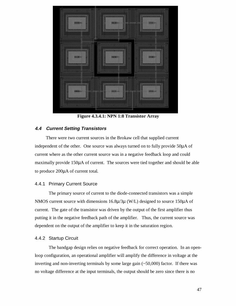
47
Figure 4.3.4.1: NPN 1:8 Transistor Array
4.4 Current Setting Transistors
There were two current sources in the Brokaw cell that supplied current
independent of the other. One source was always turned on to fully provide 50µA of
current where as the other current source was in a negative feedback loop and could
maximally provide 150µA of current. The sources were tied together and should be able
to produce 200µA of current total.
4.4.1 Primary Current Source
The primary source of current to the diode-connected transistors was a simple
NMOS current source with dimensions 16.8µ/3µ (W/L) designed to source 150µA of
current. The gate of the transistor was driven by the output of the first amplifier thus
putting it in the negative feedback path of the amplifier. Thus, the current source was
dependent on the output of the amplifier to keep it in the saturation region.
4.4.2 Startup Circuit
The bandgap design relies on negative feedback for correct operation. In an open-
loop configuration, an operational amplifier will amplify the difference in voltage at the
inverting and non-inverting terminals by some large gain (~50,000) factor. If there was
no voltage difference at the input terminals, the output should be zero since there is no

48
voltage difference to amplify. However, this is generally not the case due to offset
voltages and currents.
Upon startup, or initial powering of the Brokaw Cell, there are two possible states.
There will inherently be a difference at the terminals and this difference will be amplified
and feedback to the gate of the NMOS transistor, M1, which is being operated in the
saturation region as a current source. If the output of the amplifier is not higher than the
threshold voltage of an NMOS transistor, 0.72V, then the transistor will not fully turn on,
that is, it will stay in the triode, or linear, region. If this is the case, then there may not be
enough current supplied to create a large enough differential at the amplifier inputs. If
so, then the circuit is held in this state and a 1.25V output will never be achieved.
It is unlikely that the circuit will start in the other state with an initial voltage
difference at the amplifier terminals. To prevent that from happening, a startup circuit
was needed. In order to create a differential at the inputs large enough to drive an NMOS
transistor, a current source was needed that was also turned on as soon as the circuit was
powered. To accomplish this, a PMOS transistor, M2, with dimensions 32.4µ/3µ was
designed to supply 50µA of current when in saturation. To bias this PMOS current
source, an internal 3.5V bias was drawn from the op-amp.
Thus, when the amplifier is powered, so is the PMOS current source. The current
source will provide enough of a differential at the input terminals of the amplifier so as to
drive the NMOS transistor. Once the NMOS current source is powered, the PMOS will
continue to supply 50µA of current and will work in tandem with the NMOS transistor to
supply approximately 200µA of total current to the bipolar transistors.
4.5 Operational Transconductance Amplifier
There was no amplifier block to use in the design of the Brokaw cell so an
amplifier was made from scratch. The specifications of the amplifier were always subject
to revision and were changed often. However, it was known that the amplifier should be
a low-current device to ensure portability and minimize power consumption, and that it
would be operating from a single 5V source.
The final schematic of the amplifier is shown in Figure 4.5.1 and will be
discussed in further detail.

49
Figure 4.5.1: Amplifier Schematic
4.5.1 Input Offset Voltage
When the inputs of an amplifier are tied together, the differential between the
inputs would be zero. In an open-loop configuration, it is known that the output voltage
will be equal to the gain of the amplifier multiplied by the difference at the inputs. Thus,
if the difference of the inputs is zero, then there should be no output voltage. This is
usually not the case because a voltage due to mismatching appears at the inputs and is
amplified by the open-loop gain. This voltage is called the input offset voltage and will
be amplified causing a non-zero output despite no measurable difference at the input
The offset is due to the mismatching of loads, transistor sizes, and threshold
voltages. To minimize the offset voltage of an amplifier, attention must be paid to each
one of the above factors.
In this amplifier however, a minimal offset voltage was not crucial. Because of the
single supply, the DC operating point (when there is no differential input) would be
approximately one half of 5V, or 2.5V. Because the output of the amplifier is driving the
gate of another FET operating as a current source in the saturation region, a 2.5V output
will be enough to keep the device in saturation. If the output were to vary due to an
offset voltage, it would not affect the operation of circuit.

50
4.5.2 PMOS Current Source
To provide a bias current to the differential pair, transistors M4 and M15 were
used as a current source to provide 10.67µA of current. They were each sized with a
W/L ratio of 9/3. It is known that each device will provide equal currents because their
gate-source voltages and dimensions are equal. Also, the gate voltage of these amplifiers
was used as the 3.5V bias for the startup circuit.
4.5.3 Differential Pair
The PMOS input differential stage of the amplifier (M1, M2) was designed to draw
10.67µA from the PMOS current source when in equilibrium. The transistors were
equally sized with a W/L ratio of 36/3.
Because the bias current from the current source mentioned above cannot change,
there will always be a total of 10.67µA flowing through the two transistors. Thus, if one
transistor is fully on, then it will draw all the current from the source. If there is no
differential, then the transistors will each draw a current equal to half of the bias current,
or 5.3µA.
The outputs of the differential pair were kept separate and not converted to a single
ended output. This conversion would be done later at the output of the amplifier.
4.5.4 Active loads
A current mirror has a finite output resistance that is inversely proportional to the
current flowing through it. Also, the current source will act as a gain stage. Thus, they
are called active loads. The NMOS transistor pairs M8, M6 and M10, M19 worked as
active loads for the differential pair. All four devices were equally sized as 18/6 and
mirrored the current flowing through them.
For example, the current from M1 would be forced through M6. This current
would mirrored and also flow through M8. In equilibrium, 5,3µA would flow through
M1 and be mirrored through M8.
The purpose of M9 is to ensure that M7 operates under the same conditions as M0.
That is, its sole purpose is to provide a voltage drop for M7 and match the conditions
seen be M0. Since M7 already has its gate and drain tied together, it does need to be

51
cascoded, but still needs to be at an appropriate voltage under the same conditions as the
output stage. M9 was sized as 18/6 and biased with 2.1V from a FET ladder.
4.5.5 Biasing
To bias several of the transistors in out circuit, bias voltages needed to be set up.
This was accomplished through the use of a ladder of PMOS transistors operating in the
linear region. By providing a voltage drop of 2.1V, transistor M17 set a 2.1V bias for
both M9 and M18. Transistor M11 was also used in the ladder to ensure the correct
region of operation. Transistor M11 and M17 were sized with ratios of 9/3 and 3/3
respectively.
Likewise, another ladder was created with PMOS transistors M12, M13, and M14
to establish a 2.7V bias for transistor M5. It was designed in a similar manner, each
transistor operating in the linear region acting as resistors and providing voltage drops.
M12, M13, and M14 were sized as 3/3, 15/3, and 15/3 respectively.
4.5.6 More Current Sources
To achieve an output of 2.5V when in equilibrium, the separate outputs of the
differential pair was brought back together. Mirroring the current in device M8, M7 and
M0 will again mirror the current so that the PMOS output stage will be able to provide
5.3µA of current. The devices were matched with a W/L ratio of 30/6 each.
Also, as previously mentioned, transistor M19 will be able to sink 5.3µA of current
when the inputs are equal. Therefore, while in equilibrium, the PMOS output will
provide 5.3µA of current while the NMOS output transistor will sink 5.3µA of current. If
transistors M19 and M0 were not matched to sink and source the same currents, problems
would develop with the compensation capacitor.
4.5.7 Capacitor Compensation
To set the dominant pole in the amplifier, a capacitor was added to the output and
included in the internal design of the amplifier. Capacitors in an integrated circuit are
usually quite large, relatively speaking, and, therefore, costly since die area is expensive.

52
Because this process had 2 poly and 2 metal layers, it was possible to sandwich these
layers together and create a small capacitance which would be suitable to the task.
The goal was then to create a 3pF capacitor that would contribute a pole to the
system at approximately 100Hz. The capacitor was constructed using 4 overlapping
capacitive layers, each of the same size, which, when connected in parallel, would create
a 3pF capacitor.
Table 4.5.7.1 summarizes the different capacitances between layers available to the
designer. These were capacitances were from the N88Z run of the AMI process at
MOSIS.
Table 4.5.7.1: Capacitive layers in AMI Process
CAPACITANCEPARAMETERS
N+ACTV P+ACTV POLY POLY2 MTL1 MTL2 N_WELL UNITS
Area (substrate) 287 296 36 20 13 28 aF/µ2
Area (N+active) 1135 706 49 25 aF/µ2
Area (P+active) 1117 697 aF/µ2
Area (poly) 596 45 21 aF/µ2
Area (poly2) 45 aF/µ2
Area (metal1) 38 aF/µ2
To create the 4-layer device, it was decided that both poly and both metal layers
would be used. First, a poly layer would be put down and on top of the poly layer, a
layer of poly2 would be placed. This would act as one capacitor with a capacitance of
596 aF/µ2. Thirdly, a layer of metal-1 would be placed on top of the two poly layers
creating a second capacitance whose layers were poly2 and metal-1. This second
capacitor had the value of 45 aF/µ2. Lastly, a layer of metal-2 was added on top of the
growing stack and created a third capacitor with a value of 38 aF/µ2. Each capacitor was
connected in parallel as seen in Figure 4.5.7.1 below.
Figure 4.5.7.1: 4-layer Capacitor

53
Therefore, to create a 3pF capacitor, the equation
)38()45()596( 222 211221 µµµaF
MMaF
MPaF
PP AAAC ++= (4.5.7.1)
needed to be solved. Each area between layers was equal to create a uniformly shaped
device. The area of the capacitor calculated to be approximately 4400 µ2. To fit the
layout of the capacitor into the design easier, the capacitor was made with dimensions
126.9µ by 34.8µ.
While a poly layer over a p-active or n-active area would create a larger
capacitance in a smaller area, a device created in this fashion would not have linear
characteristics and was avoided.
Had the output stage not been matched appropriately, the capacitor would cause
problems. If, perhaps, the output PMOS mirror were to source more than 5.3µA of
current and the NMOS could, at maximum, sink only 5.3µA, then, by principle of KCL,
the remaining current must go into the output node and through the capacitor. Because
the current equation for a capacitor is equal to the capacitance times the change in
voltage, the capacitor would continuously charge while there was a current, eventually,
rupturing.
4.5.8 Cascoded Output
The output stage was also cascoded to increase the output resistance and therefore, the
open-loop gain of the amplifier. The principle behind a cascoding the output is to
increase the voltage swing available to keep the transistors in saturation.
The gate of PMOS transistor M5 was biased at 2.7V so that its gate-source and
drain-source voltage were at -.83V (VTHRESHOLD) and –1.03 respectively. This ensured
that the drain of transistor M0 did not vary and kept it in saturation. Otherwise, the
output could swing high enough to set M0 into the triode region.
NMOS transistor M18 was designed in the same manner except its gate was
biased at 2.1V. Transistor M18 had a gate-source voltage of 0.71V, which allowed
operation in the saturation region and also shielded the source of M19 from any voltage
swing.
Cascode transistors M5 and M18 had W/L ratios of 30/3 and 18/3 respectively.

54
4.5.9 Inverting and Non-Inverting Terminals
The inverting and non-inverting terminals of the amplifier are determined by
tracing a signal path to the output through the circuit. In every instance where the signal
must traverse through the gate to the drain (or vice versa), the signal becomes inverted, as
is the case with any common-source amplifier.
Using this convention, M1 is the inverting terminal since a signal from M1 to the
output undergoes three inversions. Likewise, M2 is the non-inverting terminal since a
signal would undergo two inversions thereby making it non-inverted.

55
4.5.10 Specifications of the Amplifier
The amplifier was simulated in Cadence using Analog Artist to verify its
operability. First, a DC sweep was performed across the inputs to verify that the high
gain region of the amplifier was centered as close to around zero as possible. The results
from the sweep are shown in Figure 4.5.10.1
Figure 4.5.10.1: DC Sweep of Amplifier
The high gain region is easily seen centered on 0V input, which means that there
is virtually zero offset voltage. Also, at 0V input, the output of the amplifier is
approximately 2.5V. The sloped regions extending from the high gain region occur
because of transistors M0 and M19 going into the linear operating region and drifting out
of the saturation region because they are no longer biased properly.
More information can be gathered if the high gain region is looked at more
closely. Figure 4.5.10.2 shows a zoomed view of the high gain region.

56
Figure 4.5.10.2: Zoomed View of High Gain Region
The markers A and B indicate where the amplifier left its high gain region. Also,
the slope between markers A and B indicate the open-loop gain of the amplifier is
approximately 20,000. Furthermore, it is seen that the offset voltage is actually on the
order of 174µV and not zero as assumed before.
To further characterize the amplifier, Bode plots were done to verify its open-loop
gain and phase.

57
Figure 4.5.10.3: Magnitude Bode Plot
Figure 4.5.10.3 shows the magnitude of the gain of the amplifier as it varies over
frequency. The –3dB frequency, or break frequency, of the amplifier where the gain is
70% of its maximum value occurs at a corner frequency of approximately 110Hz. In
addition, the unity gain bandwidth is approximately 2.3MHz.

58
Figure 4.5.10.4: Bode Plot of Phase Response
Figure 4.5.10.4 shows the phase response of the amplifier over frequency. The
pole at 110Hz drops the phase to 90º from 180º. There is another pole past 10MHz that
will not affect the system. At the unity-gain frequency of 2.3MHz, there is still well over
75º of phase margin so the amplifier would be stable in an open-loop configuration.

59
The final layout of the design was 164.10µ by 122.70µ (~20,135µ2) is shown
below in Figure 4.4.10.5.
Figure 4.4.10.5: Layout of Amplifier
4.6 Design of Poly Resistors
One challenge of this project is to design the values of the resistors that will produce a
1.25-volt output. Another task is to determine which resistors affect the output the most
and, ultimately, must be trimmed to meet specifications. To answer both these questions,
each node in the circuit must be analyzed to see how each resistor affects the output and
to what degree.
4.6.1 Absolute Error in Resistors Due to Process Variations
Through nodal analysis it was determined that the final equation for the bandgap
output voltage is:

60
+=
21
2
11 ln
R
R
I
I
R
RnVVV t
S
SttBEBANDGAP (4.6.1.1)
It is seen in this equation that VBANDGAP relies on the ratios of the three resistors Rt,
R2, and R3. It is known that the precise values of the resistors cannot be controlled
because of process variations and may vary by as much as 20%. Also, since all three
resistors will be made on the same die at the same time, the percentage of relative error
for each resistor should be equal. Thus, when captured in a ratio, the error term should
cancel out.
For example, in the ratio of resistance Rt to R2, each resistor can be more accurately
represented by the designed resistor value plus some relative error term, which would
then make the ratio.
22 RR
RR tt
∆+∆+
(4.6.1.2)
The error term for each resistor is an equal to some fraction of the original resistance
desired. This percentage error is the same for each resistor due to the process. Thus, the
error term effectively cancels itself and the desired original resistor ratio remains.
4.6.2 Resistor Values
Other important factors that needed attention included the absolute values of R1, R2,
and R3 as well as which resistor will be trimmed. To calculate the numerical values of
these three resistors, it was understood that R3 and R1 must be of relatively high
resistance in order to create a substantial voltage across these resistors along with
currents I1 and I2, which are the currents across these resistors respectively. The voltage
across resistors R1 and R3 is equal to the output voltage, 1.25V, minus the base-emitter
voltage of Q1. Because the base-emitter voltage will vary, the voltage across the resistor
could range from 350mV to 550mV. The current available to the resistors is 200µA and
since the voltages across each resistor are equal, will divide evenly, forcing 100µA of
current through each resistor. Thus, using Ohm's law, the resistances R1 and R3 should
be able to vary between 3.5kΩ and 5.5kΩ to account for VBE variation and keep the
output at 1.25V.

61
The resistance R2 has the voltage of ∆VBE, or,
1
2
1
3lnS
St
I
I
R
RnV (4.6.2.1)
applied across it.
Because the transistors Q1 and Q2 were designed with an emitter area ratio of 1:8,
then the saturation current density through the emitters is the inverse of that ratio, or 8:1.
It is already known that R1 and R3 should be equal and that the term nVt is equal to 26mV
at room temperature for a silicon transistor. Thus, ∆VBE should be equal to
approximately 55mV-58mV. Using Ohm's law again, with a current of 100µA flowing
through the resistor, R2 should be equal to approximately 580Ω.
4.6.3 Initial Accuracy
The final consideration was to determine which resistor(s) was to be the trimmable
resistor. The best way to determine this was to see what resistor, or resistors, affects the
output the most.
The reason one needs to trim in a bandgap circuit is due to the variation in the
saturation current, IS. As previously stated in Equation 4.6.1.1,
+=
2
3
1
2
1
31 ln
R
R
I
I
R
RnVVV
S
StBEBANDGAP (4.6.3.1)
and
=
1
11 ln
S
CtBE
I
InVV (4.6.3.2)
Through this equation it is seen that VBANDGAP will vary as IS1 varies and it is known
that IS can vary up to six times what it is originally designed for in a CMOS process. To
compensate for this variation in IS one, two, or all three of the resistors must be trimmed.
This could also be seen when simulations of the circuit were run in Cadence after
changing the IS parameter six times from 1*10-17 to 6*10-17 and stepping up R3 from
3000Ω according to actual trim resistor values, which are calculated in the next section of
this report. By taking these data points from simulations, at room temperature, a plot of
the output voltage versus the change in R3 was created. These results are shown in
Figure 4.6.3.1.

62
Figure 4.6.3.1: Graph of VBANDGAP versus R3
This graph verifies that R3 or another resistor will have to be trimmed in order to get
VBANDGAP within ±5mV initial accuracy because the operating point changes greatly due
to changes in IS.
Next, it is evaluated as to which resistor should be the trim resistor and why. By
evaluating the output equation, it is seen that R3 is in the numerator of both ratios
whereas R1 and R2 appear in the denominator of one ratio each. The ratio however of
R3/R1 is in a natural logarithm function and, because R1 should equal R3, will result in a
minute contribution to the total bandgap output. However, the ratio of R3/R2 is a direct
proportion of the two resistors. Thus, while R1 affects the output, it can be eliminated as
the trimmable resistor since it is seen that R3 and R2 are more of a factor in determining
the output voltage.
There are two resistors left that could be trimmed, but due to space constraints on
chip only one trimmable resistor will be allowed to save space. Therefore, one of the two
remaining resistors R2 or R3 needs to be eliminated as the trimmable resistor. Taking this
into account, R2 can be eliminated because of its small value of resistance. In order to
trim a resistor using a link fuse technique, many steps of geometrically increasing
resistors are needed to provide maximum resolution and to ensure that the proper output
could be achieved. Thus, resistor R3 was decided to be the trimmable resistor because it
would be on the scale of 3.5kΩ to 5.5kΩ. With a large resistor of this magnitude, it is
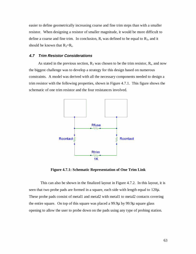
63
easier to define geometrically increasing coarse and fine trim steps than with a smaller
resistor. When designing a resistor of smaller magnitude, it would be more difficult to
define a coarse and fine trim. In conclusion, Rt was defined to be equal to R3, and it
should be known that R3=Rt.
4.7 Trim Resistor Considerations
As stated in the previous section, R3 was chosen to be the trim resistor, Rt, and now
the biggest challenge was to develop a strategy for this design based on numerous
constraints. A model was derived with all the necessary components needed to design a
trim resistor with the following properties, shown in Figure 4.7.1. This figure shows the
schematic of one trim resistor and the four resistances involved.
Figure 4.7.1: Schematic Representation of One Trim Link
This can also be shown in the finalized layout in Figure 4.7.2. In this layout, it is
seen that two probe pads are formed in a square, each side with length equal to 120µ.
These probe pads consist of metal1 and metal2 with metal1 to metal2 contacts covering
the entire square. On top of this square was placed a 99.9µ by 99.9µ square glass
opening to allow the user to probe down on the pads using any type of probing station.
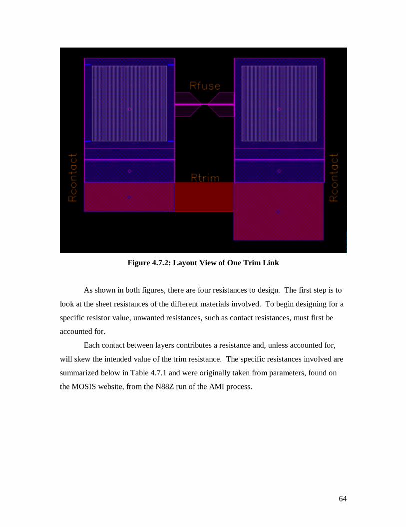
64
Figure 4.7.2: Layout View of One Trim Link
As shown in both figures, there are four resistances to design. The first step is to
look at the sheet resistances of the different materials involved. To begin designing for a
specific resistor value, unwanted resistances, such as contact resistances, must first be
accounted for.
Each contact between layers contributes a resistance and, unless accounted for,
will skew the intended value of the trim resistance. The specific resistances involved are
summarized below in Table 4.7.1 and were originally taken from parameters, found on
the MOSIS website, from the N88Z run of the AMI process.

65
Table 4.7.1: MOSIS Resistance Parameters for the AMI 1.2µ ProcessComponent Color
( in Figure 4.7.2)
Material Resistance
Rtrim Red Poly 29.0 Ω/
Rfuse Pink Metal2 0.03 Ω/
Rcontact Purple Metal2 to Metal1 0.05 Ω
Rcontact Red/Purple Metal1 to Poly 32.5 Ω
In order to design an accurate geometrically increasing trimmable resistor with
contacttrimt RRR 2+= (4.7.1)
both Rtrim and Rcontact must have equal step sizes. For example if the first link of Rt =
1kΩ, where Rtrim = 960Ω and Rcontact = 20Ω, the next step in the trim should equal (1k/2)
or 500Ω, where Rtrim = (960/2) or 480Ω and Rcontact = (20/2) or 10Ω each. If this can be
accomplished, it would be a true geometrically increasing resistor.
With this in mind, a trimmable resistor with a base resistance of 3.0kΩ was
designed with a coarse trim ranging from 1.065KΩ to 33.2Ω and a fine trim ranging from
33.6Ω to 1.8Ω. This resistor therefore has the potential to be trimmed anywhere from
3.0kΩ to 5.164kΩ.
These values were designed by fixing the largest trim resistor and geometrically
stepping down to design the rest of the trims. This first trim resistor consists of a Rtrim
value equal to 1kΩ with one contact on both sides equal to 32.5Ω each. Thus, the total
resistance would equal 1.065Ω. By placing the 1kΩ resistor (Rtrim) in parallel with a copy
of itself, it is possible to directly step down the resistance by a factor two, making the
new Rtrim = 500Ω. Creating double the contacts (in parallel) also cuts the contact
resistance in half to 16.25Ω. The total resistance (Rt) is now equal to (1065/2)Ω or
532.5Ω, and follows Equation 4.7.1 because 500 + 2*16.25 = 532.5. This technique was
used in designing all the coarse trim resistors.
The fine trim resistors were then designed on the same principle but starting at
33.6Ω, a higher resistor value than the last coarse trim resistor (33.2Ω) to compensate for
any lost resolution that might occur in the trim procedure. Even though it was desirable

66
to produce poly resistors and contacts with the same step size, the smaller resistors
needed extra contacts to further minimize resistance and therefore, the last three resistors
in the fine trim were scaled differently from the first three resistors. The fine trim thus
consisted of linked resistors ranging in magnitude from 33.6Ω to 1.8Ω. The final layout
of this link-fused resistor along with the base 3.0kΩ resistor is shown in Figure 4.7.3
below. The number "1" is also laid out on chip using metal1 to denote the start of the
fine trim along with the number "14" to indicate the last coarse trim in the trim resistor.
Figure 4.7.3: Layout of complete trim resistor with a base resistor of 3.0KΩ
One final aspect of this resistor is the length of the metal2 fuse that is placed in-
between the probe pads. The length of this fuse was determined based on principles of
maximum current allowed through a metal2 wire. This principle states that a current
equal to or greater than I will break or blow up a wire with diameter d in inches. This
equation, found in many common engineers' handbooks, is:
2/3dKI ⋅= (4.7.2)
The fuse was designed out of metal2 and the characteristics in the handbook state
that for metal2 K=7585. This equation is based on a circular wire with a given radius
but, when designing in Cadence, all components are designed based on square values.
First a current was calculated that would blow a minimum sized metal2 wire of length

67
and width 1.8µm. This wire has an area of 3.24µm2 and when converted to inches,
equals 5.022*10-09inches2. This was calculated using the conversion factor:
mE
cm
cm
inm
µµ
41
1
54.2
11 ⋅⋅ (4.7.3)
We also know that in a circular solid strand wire, the area is equal to
2rarea ⋅= π (4.7.3)
Therefore, substituting in the previously calculated area, r is equal to 3.99*10-05 inches.
If r=3.99*10-05 inches and K=7585, then the current needed to blow that wire I should be
any value greater than or equal to: .42.5 mAI ≥
4.8 Non-inverting Gain Amplifier
To boost the output of the 1.25V-bandgap voltage to 2.5V, the amplifier from the
Brokaw Cell was modified and used in a non-inverting configuration with a gain of
approximately 2.
4.8.1 Amplifier Modifications
The original amplifier designed to drive the NMOS current source from before was
slightly modified to provide twice the output current as before, or 10.67µA. The PMOS
output transistors M0 and M5 had doubled widths with new dimensions of 60/3 and 60/3
respectively. The NMOS transistors M18 and M19 also needed to be able to sink twice
the current and had new dimensions of 36/3 and 36/6 respectively. The new schematic
and layout of the amplifier, which measured 192.90µ by 124.80µ (~24,073.92µ2), (can be
seen in Figure 4.8.1.1 and 4.8.1.2 respectively. No other modifications were made.

68
Figure 4.8.1.1: Schematic of the Non-Inverting Gain Amplifier
Figure 4.8.1.2: Layout of the Non-Inverting Gain Amplifier

69
4.8.2 Gain Setting
To boost the bandgap voltage from 1.25 volts, the modified amplifier was used in
the non-inverting configuration. Because the output current of the amplifier was small,
large resistors would be needed to provide the appropriate feedback to the inverting
terminal. Due to area considerations, large poly resistors were avoided. Instead, two
PMOS transistors were operated in the triode region to provide the appropriate feedback.
The voltage required at the inverting terminal to provide an output of 2.5V was
equal to 1.25, the bandgap voltage for this circuit. Transistors M1 and M2 were designed
W/L ratios of 8.1/3 and 21.4/3 respectively. The reason being is that M1 and M2 must
drive equal currents while providing the necessary drop of 1.35 volts and 1.25 volts each.
With this configuration, the PMOS transistors act as gain setting resistors and the input is
amplified to 2.5 volts.
Figure 4.8.2.1: Schematic of Output Buffer
4.9 Final Layout
All of the pieces that were designed in the previous steps need to be combined to
form a complete bandgap circuit. The individual building blocks were combined on a
single layout.
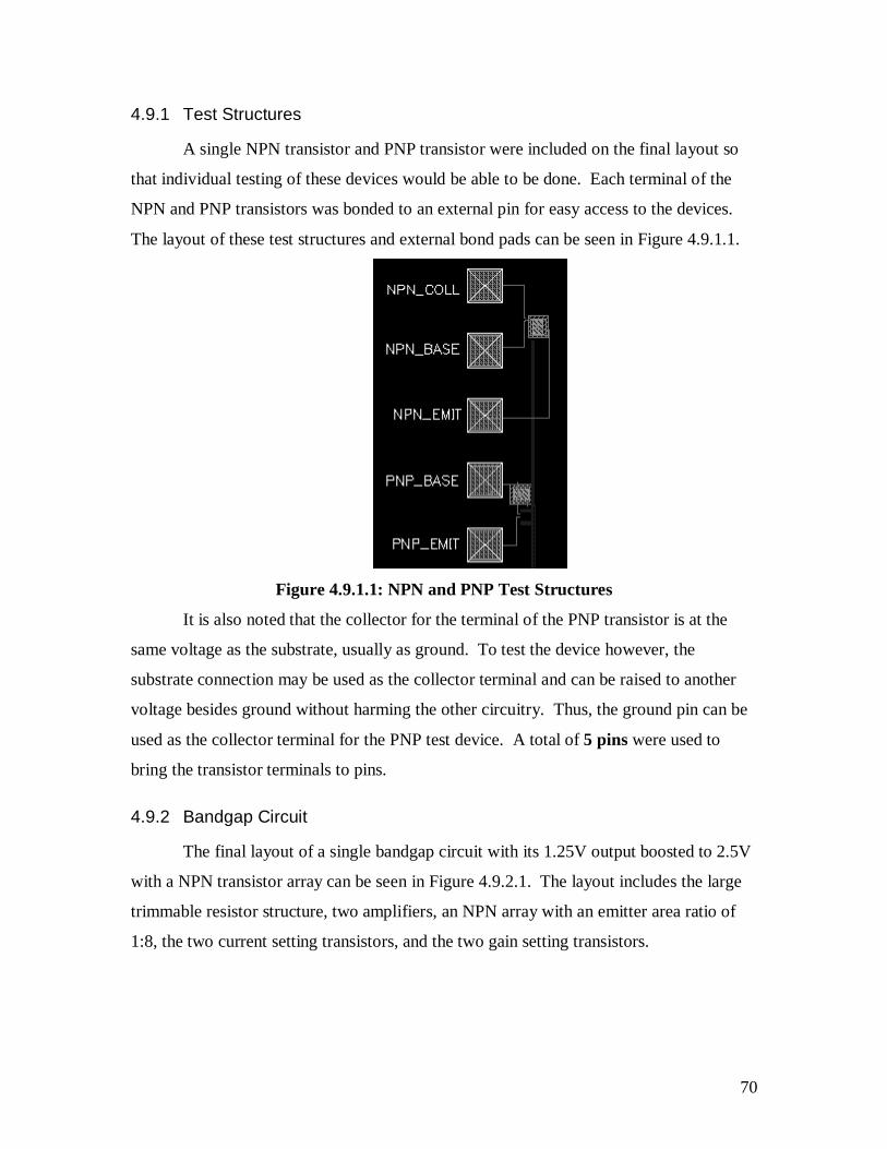
70
4.9.1 Test Structures
A single NPN transistor and PNP transistor were included on the final layout so
that individual testing of these devices would be able to be done. Each terminal of the
NPN and PNP transistors was bonded to an external pin for easy access to the devices.
The layout of these test structures and external bond pads can be seen in Figure 4.9.1.1.
Figure 4.9.1.1: NPN and PNP Test Structures
It is also noted that the collector for the terminal of the PNP transistor is at the
same voltage as the substrate, usually as ground. To test the device however, the
substrate connection may be used as the collector terminal and can be raised to another
voltage besides ground without harming the other circuitry. Thus, the ground pin can be
used as the collector terminal for the PNP test device. A total of 5 pins were used to
bring the transistor terminals to pins.
4.9.2 Bandgap Circuit
The final layout of a single bandgap circuit with its 1.25V output boosted to 2.5V
with a NPN transistor array can be seen in Figure 4.9.2.1. The layout includes the large
trimmable resistor structure, two amplifiers, an NPN array with an emitter area ratio of
1:8, the two current setting transistors, and the two gain setting transistors.

71
Figure 4.9.1.2: Single Bandgap Circuit #2 with NPNs

72
4.9.3 Pin Assignments
The pin assignments were somewhat arbitrary and pins were conveniently
assigned as necessary from the layout view. It was decided that the first bandgap circuit
on the chip, which was made with PNP transistors, would be the primary circuit and
should include the most test points so that every node in the circuit could be analyzed.
These points included:
• Ground• The base-emitter voltages of the first transistor, used to calculate the actual difference
in base-emitter voltage• The base-emitter voltages of the second transistor, used for the same reasons• The voltage at the negative terminal of the first amplifier, so that the actual offset of
the amplifier could be measured• The 3.5V bias at the gate of the startup transistor• The output of the amplifier driving the primary current source• The 1.25V bandgap output, which feeds into the positive terminal of the second
amplifier• The voltage at the negative terminal of the second amplifier• The final 2.5V output voltage.• Each bandgap circuit was also given their own power connection
These pin assignments for the primary bandgap circuit consumed 10 of the 40 pins
available on the chip.
For the second bandgap circuit, made with NPN transistors, not as many test
points were required because many of the measurements would be the same as the first
circuit. Thus, the pins were assigned as follows:
• Base-emitter voltage of Q1• Base-emitter voltage of Q2• The 1.25V output• The 2.5V output• The output of the first amplifier• Power• Ground
It was determined that the circuit could be evaluated with these test points only and used
7 pins.
The third bandgap circuit also used PNP transistors. Due to a shortage of area on
the chip, the trim resistor structure was altered such that the 100µ square probe pads were
not used and that to blow the links, external pins could be used just as easily. Thus, the

73
links were brought to bond pads on the chip and an approximate 1400µ2 of area was
saved. This space-saving design of the trimmable resistor used 13 pins.
Thus, a total of 35 pins had already been assigned among, the two other bandgap
circuits, test devices, and trim resistor, leaving only 5 pins left for the third bandgap
circuit. The pins brought to bond pads in this final circuit included:
• The base-emitter voltage of Q1
• The base-emitter voltage of Q2
• The 1.25V output voltage• The 2.5V output voltage• Power
It was decided that it was necessary for the circuit to be powered separately, but that the
ground connection for the second and third bandgap circuits could be shared.
The final assignment of each pin is summarized in Table 4.9.3.1 and is shown in a
manner which is representative of looking at an actual chip, that is, Pin #1 is in the upper
left corner while Pin #40 is in the upper right corner.

74
Table 4.9.3.1: Pin Assignments
Pin
NumberDescription
Pin
NumberDescription
1 VDD 40 1.25V Bandgap
2 VBE, 8X Emitter 39 2.5V Output
BG#3
Ba
ndg
ap
#3
3 VBE, 1X Emitter 38 Amplifier 1 Output
4 End of trim resistor: 1.8 37 Ground
5 1.8, 2.6 36 VDD
6 2.6, 4.5 35 2.5V Output
7 4.5, 8.4 34 VBE, 8X Emitter
8 8.4, 16.8 33 VBE, 1X Emitter
9 16.8, 33.2 32 1.25V Bandgap Output
Ba
ndga
p #2
10 33.2, 33.6 31 Negative Terminal of 2nd Amplifier
11 33.6, 66.5 30 2.5V Output
12 66.5, 133 29 1.25V Bandgap Output
13 133, 266 28 Amplifier 1 Output
14 266, 562 27 3.5V Bias
15 562, 1065 26 VDD
Ba
ndg
ap
#3 T
rim
Res
isto
r
16 End of trim resistor: 1065 25 Ground
17 NPN Collector 24 VBE, 1X Emitter
18 NPN Base 23 VBE, 8X Emitter
19 NPN Emitter 22 ∆VBE
Ba
ndga
p #1
Tes
t D
evic
es
20 PNP Base 21 PNP Emitter
The final layout of all three bandgap circuits is shown in Figure 4.9.3.1.

75
Figure 4.9.3.1: Layout view of Final Design
This top-level layout is also shown in Figure 4.9.3.2 in schematic form on the following
page.

76
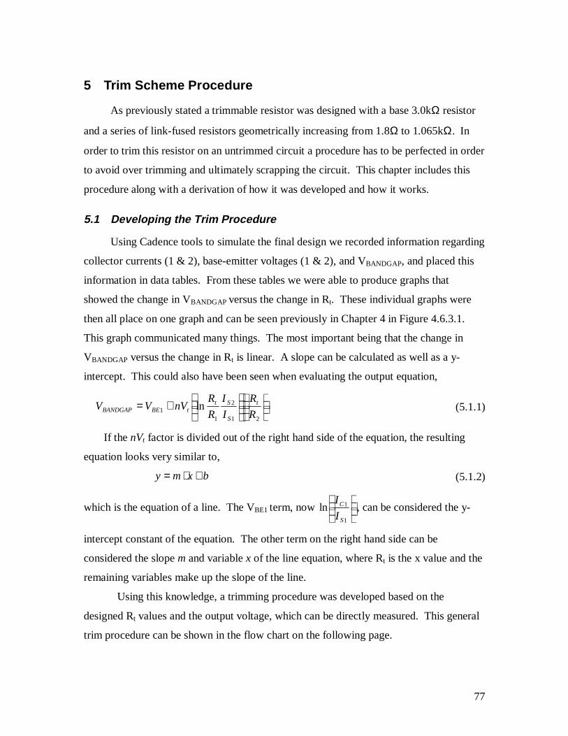
77
5 Trim Scheme Procedure
As previously stated a trimmable resistor was designed with a base 3.0kΩ resistor
and a series of link-fused resistors geometrically increasing from 1.8Ω to 1.065kΩ. In
order to trim this resistor on an untrimmed circuit a procedure has to be perfected in order
to avoid over trimming and ultimately scrapping the circuit. This chapter includes this
procedure along with a derivation of how it was developed and how it works.
5.1 Developing the Trim Procedure
Using Cadence tools to simulate the final design we recorded information regarding
collector currents (1 & 2), base-emitter voltages (1 & 2), and VBANDGAP, and placed this
information in data tables. From these tables we were able to produce graphs that
showed the change in VBANDGAP versus the change in Rt. These individual graphs were
then all place on one graph and can be seen previously in Chapter 4 in Figure 4.6.3.1.
This graph communicated many things. The most important being that the change in
VBANDGAP versus the change in Rt is linear. A slope can be calculated as well as a y-
intercept. This could also have been seen when evaluating the output equation,
+=
21
2
11 ln
R
R
I
I
R
RnVVV t
S
SttBEBANDGAP (5.1.1)
If the nVt factor is divided out of the right hand side of the equation, the resulting
equation looks very similar to,
bxmy +⋅= (5.1.2)
which is the equation of a line. The VBE1 term, now
1
1lnS
C
I
I, can be considered the y-
intercept constant of the equation. The other term on the right hand side can be
considered the slope m and variable x of the line equation, where Rt is the x value and the
remaining variables make up the slope of the line.
Using this knowledge, a trimming procedure was developed based on the
designed Rt values and the output voltage, which can be directly measured. This general
trim procedure can be shown in the flow chart on the following page.

78
Figure 5.1.1: Flow Chart of Trim Procedure
This procedure requires an initial trim to be made in order to start making any
calculations of slope, y-intercept, or trim resistor values. The flow chart simply states
that the value of VBANDGAP is measured and the circuit is then trimmed according to the
calculations and actual resistor values. Even though the actual resistor values in the
design are process dependent and can vary by up to 20 percent, the actual designed values
can be used in these calculations because the resistor ratios will never change with
respect to any change in sheet resistance.

79
The calculations shown below are the calculations that are needed in order to use the
trim procedure.
• Calculating the slope of the line:
−−
=oldtnewt
BANDGAPBANDGAP
RR
VVm
__
1_2_
(5.1.3)
• Calculating the y-intercept of the line:
,22_ bslopeRV tBANDGAP +⋅= (5.1.4)
solve for b and the equation is:
slopeR
Vb
t
BANDGAP
⋅= 2_
(5.1.5)
• Using the previously calculated values for slope and y-intercept and lettingVBANDGAP=1.25 (the desired value), x can be calculated and considered the value of Rt
needed to trim to 1.25 volts. This is shown in the following equation:
slope
bx
−= 25.1(5.1.6)
• Next, calculating the amount of resistor needed to complete this trim is performed bysubtracting the new Rt value by the old one, called ∆Rt. The equation for ∆Rt equals:
previousRx − (5.1.7)
where x=Rt_new.
The trim procedure that follows calls for these calculations and the formulas will be
provided in the actual procedure section.
5.2 Actual Trim Procedure
Provided on separate pages are the procedure used to trim the circuit to a 1.25-volt
output, along with a filler page for calculations and measurements that will allow the user
to fill in the blanks when trimming the bandgap circuit. A note should be made that this

80
trim procedure should only be used when trimming bandgap circuit #2 and should be
used in conjunction with the test procedure in Chapter 6.
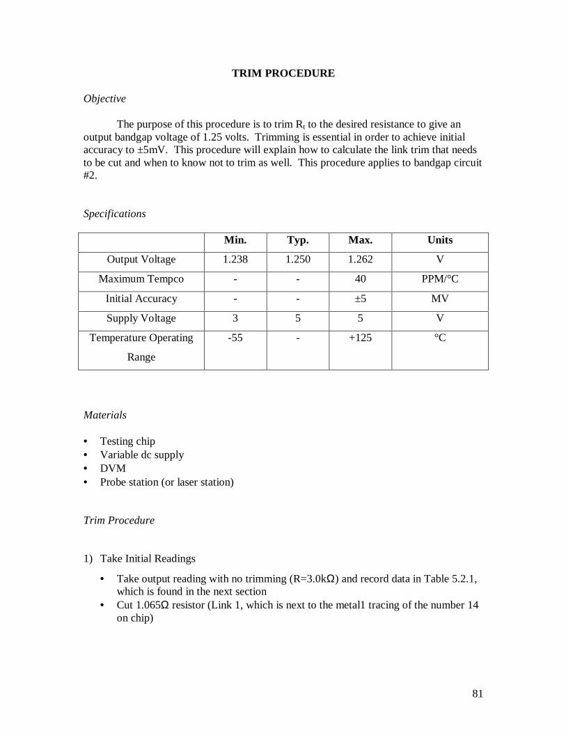
81
TRIM PROCEDURE
Objective
The purpose of this procedure is to trim Rt to the desired resistance to give anoutput bandgap voltage of 1.25 volts. Trimming is essential in order to achieve initialaccuracy to ±5mV. This procedure will explain how to calculate the link trim that needsto be cut and when to know not to trim as well. This procedure applies to bandgap circuit#2.
Specifications
Min. Typ. Max. Units
Output Voltage 1.238 1.250 1.262 V
Maximum Tempco - - 40 PPM/°C
Initial Accuracy - - ±5 MV
Supply Voltage 3 5 5 V
Temperature Operating
Range
-55 - +125 °C
Materials
• Testing chip• Variable dc supply• DVM• Probe station (or laser station)
Trim Procedure
1) Take Initial Readings
• Take output reading with no trimming (R=3.0kΩ) and record data in Table 5.2.1,which is found in the next section
• Cut 1.065Ω resistor (Link 1, which is next to the metal1 tracing of the number 14on chip)

82
2) Calculations (All equations are given on Measurements and Calculations page)
• Take output reading and record in Table 5.2.1• Add previous resistor value in Table 5.2.1 to the value of link just cut and record
in next open slot in table• Determine slope (m value in equation y=mx+b )• Determine offset of line (b value)• Solve for Rtrim (value of x) if y=1.25, and using the m and b values solved for in
previous two steps• Subtract x from Rprevious to get ∆Rtrim
3) Cutting Links
Coarse Trim Begins Here• Is 532.5 greater than ∆Rtrim?
♦ If yes, then do not cut link 2 and move to next step♦ If no, then cut link 2 and return to step 2) Calculations
• Is 266.25 greater than ∆Rtrim?♦ If yes, then do not cut link 3 and move to next step♦ If no, then cut link 3 and return to step 2) Calculations
• Is 133.125 greater than ∆Rtrim?♦ If yes, then do not cut link 4 and move to next step♦ If no, then cut link 4 and return to step 2) Calculations
• Is 66.56 greater than ∆Rtrim?♦ If yes, then do not cut link 5 and move to next step♦ If no, then cut link 5 and return to step 2) Calculations
• Is 33.6 greater than ∆Rtrim?♦ If yes, then do not cut link 7 and move to next step♦ If no, then cut link 7 and return to step 2) Calculations
Fine Trim Begins Here• Is 33.2 greater than ∆Rtrim?
♦ If yes, then do not cut link 6 and move to next step♦ If no, then cut link 6 and return to step 2) Calculations
• Is 16.8 greater than ∆Rtrim?♦ If yes, then do not cut link 8 and move to next step♦ If no, then cut link 8 and return to step 2) Calculations
• Is 8.4 greater than ∆Rtrim?♦ If yes, then do not cut link 9 and move to next step♦ If no, then cut link 9 and return to step 2) Calculations
• Is 4.5 greater than ∆Rtrim?♦ If yes, then do not cut link 10 and move to next step♦ If no, then cut link 10 and return to step 2) Calculations

83
• Is 2.6 greater than ∆Rtrim?♦ If yes, then do not cut link 11 and move to next step♦ If no, then cut link 11 and return to step 2) Calculations
• Is 1.8 greater than ∆Rtrim?♦ If yes, then do not cut link 12 and move to next step♦ If no, then cut link 12 and return to step 2) Calculations
• End of Process

84
Measurements and Calculations Page
Table 5.2.1: Measuring Output versus the Change in RtVBANDGAP (V) Rt (Ω)
3000
Calculations:
30004065−== mslope
=b
=−=m
bx
25.1
=−=∆ previoust RxR
*Consult Trim Procedure for instructions on how to use this page and continue untilVBANDGAP = 1.25 volts

85
6 Test Procedure
Testing is a necessity in any design. It is important to test and try to meet
specifications, and if they are not met, corrections are made accordingly. The testing of
the IC was very important in the research and development of the chip. The trimming of
the resistors was based on the values obtained from the testing. The results obtained by
this testing can be used to correct mistakes in the continuation of the bandgap design.
6.1 Designing the PC Board
The test procedure required a test circuit in order to obtain readings that would be
more accurate than readings from a breadboard. The design of this PCB was done on
PADS, a CAD software for designing schematics and laying out PCBs. The design can be
seen in figure 6.1.1. The board is very simple; it is made up of connectors, capacitors,
traces and a DIP. The capacitors were surface mounted on the bottom of the board so
they could be as close to the IC as possible. The capacitors practically eliminate the
problem of inductance created over the length of the wires and traces. Two connectors
were used for each setup so it would be easier to make DVM readings. The board is two
layered, and was fabricated by ABC circuits.
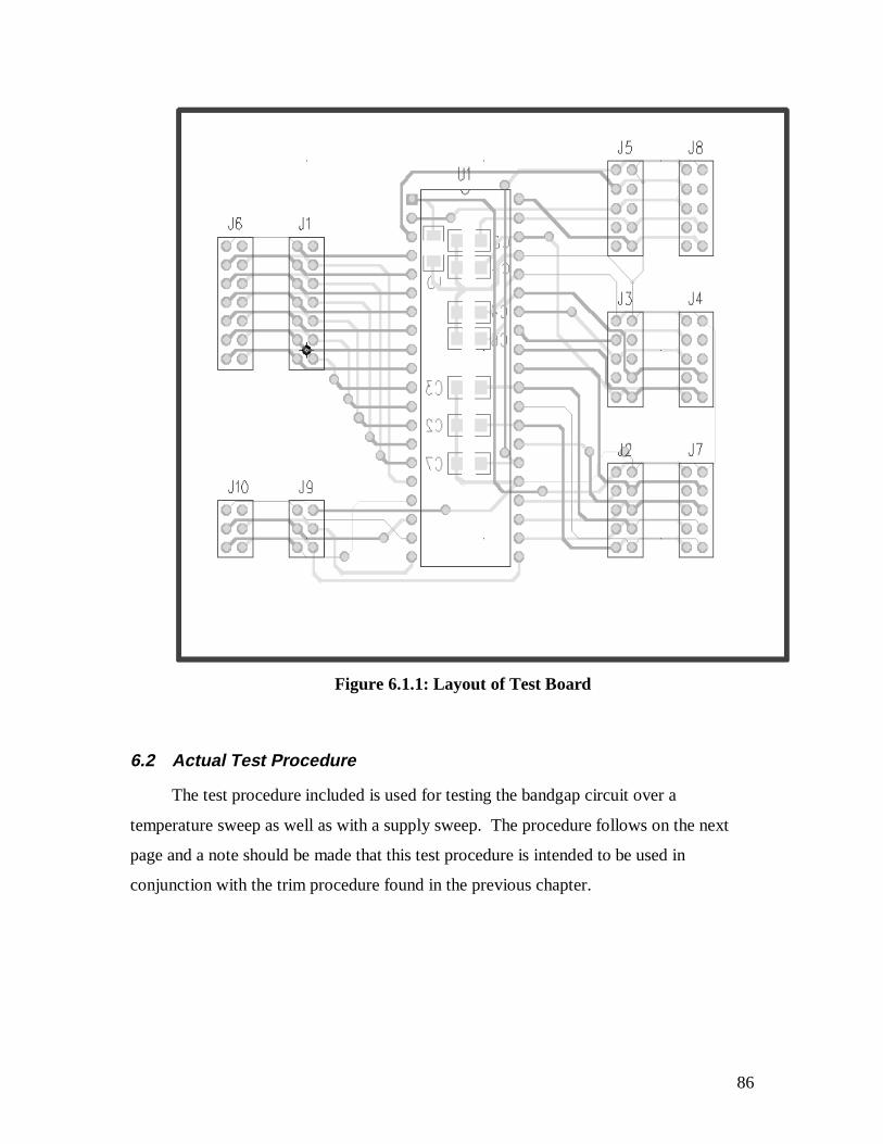
86
Figure 6.1.1: Layout of Test Board
6.2 Actual Test Procedure
The test procedure included is used for testing the bandgap circuit over a
temperature sweep as well as with a supply sweep. The procedure follows on the next
page and a note should be made that this test procedure is intended to be used in
conjunction with the trim procedure found in the previous chapter.

87
TEST PROCEDURE
Objective
The purpose of this procedure is to test the voltage reference chip and comparethe results to specifications that have been previously set. The testing is of greatimportance to the trim scheme so that it is known how much to trim. Three bandgapcircuits and two test transistors will be tested in this procedure. As of this writing,previous data regarding pnp transistors being made using a CMOS process wasunavailable, so it is imperative to test the transistors separately for research purposes.
Specifications
Min. Typ. Max. Units
Output Voltage 1.238 1.250 1.262 V
Maximum Tempco - - 40 PPM/°C
Initial Accuracy - - ±5 MV
Supply Voltage 3 5 5 V
Temperature Operating
Range
-55 - +125 °C
Materials
• Testing chip• Variable dc supply• DVM• Temperature control chamber• Heat gun• Female plugs and wires• Temperature probe• HP VEE
Procedure for Bandgap Circuit
1) Testing untrimmed circuit at typical conditions• Connect variable supply and DVM• Set supply to 5V and temperature to 25°C

88
• Record output• Trim, according to trim procedure, until desired 1.25V output is achieved
2) Testing trimmed circuit with supply voltage sweep at room temperature• Set supply to 3V• Record output voltage• Slowly increase voltage• Record output for every tenth of a volt increase stopping at 5V
3) Testing trimmed circuit with temperature sweep at 5V• Set up HP VEE program and connect to test circuit• Place test circuit in temperature controlled chamber• Set temperature probe next to circuit and close box• Set supply voltage to 5V• Turn Heat gun on and aim it into a cut out hole in the box• When the temperature probe reads max temperature, turn off heat gun and run HP
VEE until probe reads room temperature

89
7 Test Results
After the five chips had been fabricated and returned after eight weeks of fab time,
testing of the design began. Armed with the trim and test procedures, the circuits were
powered up and tested.
A die photo of the entire chip with individual bandgap circuits and test structures
marked is seen in Figure 7.1
Figure 7.1: Die Photo of Entire Chip

90
7.1 Test Preparation
Before testing began, several steps were taken to ensure that tests ran smoothly. First,
a controlled temperature chamber was constructed. A stiff cardboard box was used as this
chamber and access holes were carved in either end. The test board was put in the box
and connections to the circuit were routed through one end of the box. These connections
included power, ground, measurement probes, and a thermocouple. On the other end, a
heat gun was used to bring the box up to the desired temperature.
To power the circuit, a Tektronix PS2521G Programmable Power Supply was set to
5V with a current limit of 1mA. The output voltage was measured using a Hewlett-
Packard 3458A multimeter. The temperature of the chamber was measured using an
Extech Temperature Sensor with a Type K thermocouple. This device was mounted as
close to the die as possible without opening the packaged chip. There was a cause of
error but a better way of measuring and controlling temperature was not devised. The
thermocouple output a voltage that was directly relational to the temperature by 1mV/ºC.
This voltage was measured using a Hewlett-Packard 34401A multimeter.
Both meters were able to be programmed using HP-VEE v4.01. This allowed the
programming of the instruments to take a set number data points from each instrument
over time and plot them. After writing the code using visual objects, a user interface was
created to ease in the testing.

91
7.2 NPN Test
The first test to ensure that the bipolar transistors operated correctly was to use a
Tektronix 571 Curve Tracer to plot IB vs. VCE characteristics. The graphical output of the
curve tracer can be seen below in Figure 7.2.1.
Figure 7.2.1: IB vs. VCE for NPN Transistor
The base current was swept at different base currents and the collector-emitter
voltage was plotted. The active and saturation regions are clearly marked and verify the
operation of the transistor.
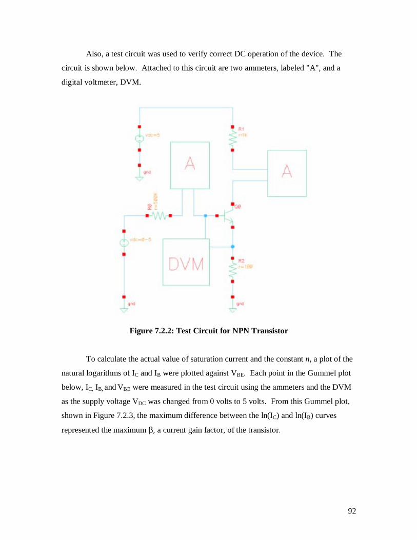
92
Also, a test circuit was used to verify correct DC operation of the device. The
circuit is shown below. Attached to this circuit are two ammeters, labeled "A", and a
digital voltmeter, DVM.
Figure 7.2.2: Test Circuit for NPN Transistor
To calculate the actual value of saturation current and the constant n, a plot of the
natural logarithms of IC and IB were plotted against VBE. Each point in the Gummel plot
below, IC, IB, and VBE were measured in the test circuit using the ammeters and the DVM
as the supply voltage VDC was changed from 0 volts to 5 volts. From this Gummel plot,
shown in Figure 7.2.3, the maximum difference between the ln(IC) and ln(IB) curves
represented the maximum β, a current gain factor, of the transistor.

93
Figure 7.2.3: Gummel Plot to Calculate IS and n for NPN Transistor
The saturation current and factor n were calculated by breaking down the equation
for the collector current of a transistor as follows.
)ln(ln t
BE
Vn
V
SC eII ⋅⋅= (7.2.1)
Using the properties of natural log functions, this equation can be simplified further to fit
the equation a line.
Bt
BEC I
Vn
VI lnln +
⋅= (7.2.2)
By setting the slope of ln (IC) vs. VBE equal to tVn⋅
1, as shown in equation 7.2.3,it
is possible to solve for n at room temperature, where Vt = 26mV.
tVnmslope
⋅==
1(7.2.3)
Calculation of Is and n
-16.05
-15.05
-14.05
-13.05
-12.05
-11.05
-10.05
-9.05
-8.05
-7.050.6326 0.6826 0.7326 0.7826
Vbe (V)
Ln(I
) ln(Ic)
ln(Ib)

94
For the NPN designed in this project, a slope of 35.461 was measured and a value
of 1.08 was calculated for n, this measurment is shown below in Figure 7.2.4. Once n
was calculated, the y-intercept, ln (IS) could be determined by using any two points on the
ln(IC) vs. VBE curve. In doing so, IS was found to be equal to 1.60*10-15. The saturation
current was expected to be approximately 3*10-15 and n would ideally be 1.00. The
maximum β for this transistor was 167.14 and occurred at an IC of 198.6µA. It was
important to operate the transistors at maximum β because β is a function of a quadratic
equation and, by using the maximum value, the drifting of β was minimized.
Figure 7.2.4: Slope of line ln(IC) vs. VBE for NPN
Through these measurements, along with using nodal analysis of the test circuit, it was
verified that the NPN bipolar transistors were operational and a successfully designed. A
die photo of the NPN array is shown in Figure A9 in Appendix A.
7.3 PNP Test
As with the NPN transistor, the first test preformed was designed to use the
Tektronix 571 Curve Tracer to plot IB vs. VCE characteristics. The graphical output of the
curve tracer can be seen below in Figure 7.3.1.
Calculating Slope
y = 35.461x - 34.021
-11.64
-11.14
-10.64
-10.14
-9.64
-9.14
-8.640.6326 0.6526 0.6726 0.6926 0.7126
Vbe (V)
Ln(I
)

95
Figure 7.3.1: IB vs. VCE for PNP transistor
Also, a test circuit was developed to verify correct DC operation of the device. The
circuit is shown below, and like the test circuit for the NPN it utilizes two ammeters and a
DVM to measure the currents IB, IC and the voltage VBE.

96
Figure 7.3.2: PNP Test Circuit
Once again, to calculate the actual values of saturation current and the constant n,
a plot of the natural logarithms of IC and IB were plotted against VBE. From the Gummel
plot in Figure 7.3.3, the maximum difference between the ln(IC) and ln(IB) curves
represented the maximum β, a current gain factor, of the transistor.
Figure 7.2.3: Gummel Plot to Calculate IS and n for a PNP device
Calculation of Is and n
-20.32
-18.32
-16.32
-14.32
-12.32
-10.32
0.48500 0.53500 0.58500 0.63500 0.68500 0.73500 0.78500 0.83500
Vbe (V)
Ln(I) Ln(Ic)
Ln(Ib)
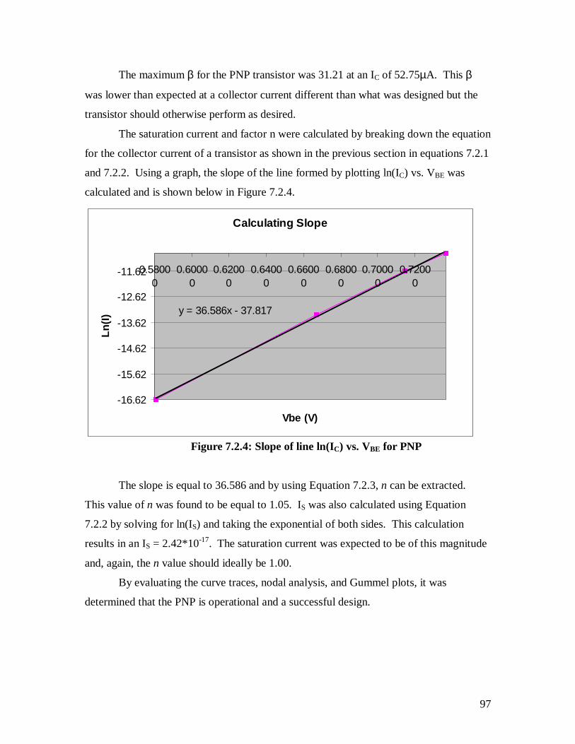
97
The maximum β for the PNP transistor was 31.21 at an IC of 52.75µA. This β
was lower than expected at a collector current different than what was designed but the
transistor should otherwise perform as desired.
The saturation current and factor n were calculated by breaking down the equation
for the collector current of a transistor as shown in the previous section in equations 7.2.1
and 7.2.2. Using a graph, the slope of the line formed by plotting ln(IC) vs. VBE was
calculated and is shown below in Figure 7.2.4.
Figure 7.2.4: Slope of line ln(IC) vs. VBE for PNP
The slope is equal to 36.586 and by using Equation 7.2.3, n can be extracted.
This value of n was found to be equal to 1.05. IS was also calculated using Equation
7.2.2 by solving for ln(IS) and taking the exponential of both sides. This calculation
results in an IS = 2.42*10-17. The saturation current was expected to be of this magnitude
and, again, the n value should ideally be 1.00.
By evaluating the curve traces, nodal analysis, and Gummel plots, it was
determined that the PNP is operational and a successful design.
Calculating Slope
y = 36.586x - 37.817
-16.62
-15.62
-14.62
-13.62
-12.62
-11.620.58000
0.60000
0.62000
0.64000
0.66000
0.68000
0.70000
0.72000
Vbe (V)
Ln(I
)

98
7.4 Amplifier Test Results
Since there were no separate amplifiers on chip, the only testing that could be done
were with amplifiers that were already included in a bandgap circuit. Had there been
more than 40 pins, a test amplifier could have been made.
A voltage source was injected at the non-inverting terminal of the buffer on the first
circuit. Measurements were made at the inverting terminal and the output to observe the
gain linearity and offset variation due to changes in the input. The gain of the amplifier is
almost linear when operated in a closed loop configuration. Figure 7.4.1 shows the
output of the buffer plotted against the input at the non-inverting terminal. The gain of
the amplifier closely follows an ideal gain of 2.07.
Figure 7.4.2: Gain Non-Linearity
Figure 7.4.2 shows the difference between the ideal gain and the gain of the
amplifier in this closed loop configuration.

99
Figure 7.4.3: Absolute Difference of Gains
It can be seen that the amplifier exhibits nearly linear gain over the input range of
0.7 to 1.3V and the gain drops off when operating past 1.3V.
To further measure the gain of the amplfier, the output was plotted against the
input differential. The slope of the linear region of the plot in Figure 7.4.4 is the gain of
the amplifier in this non-inverting gain configuration.
Figure 7.4.4: VOUT vs. VID
100
In the linear gain region at 0V differential input, the gain is approximately 25 but at
2.5V (the output of the buffer) the gain is only 4.3. A die photo of the amplifier was
taken and is shown in Figures A3 and A4 of Appendix A.
7.5 Problems with Probe Station Functionality
One initial problem encountered when testing the IC was that the probe station was
not working properly. The needles attached to the prober did not appear to make the firm
electrical connections that were needed. To verify this, the needles were shorted together
and attached to an ohmmeter. The ohmmeter read an open circuit and it was concluded
that the probe manipulators might have been faulty. Also, when these needles probed the
ends of a poly resistor, the ohmmeter still saw an open circuit. It was then concluded that
the probe manipulators were defective and that cutting links on chip could not be done
with that particular station.
To compensate for a dysfunctional probe station, another probe station was brought
into lab to be used for cutting the links in circuits 1 and 2. Even with the new probe
station, it was still not possible to trim the circuits because the arm lengths of needles
cold not reach the probe pads. While the chip could be moved under the pins, the
microscope could not see the pins and the chip in the same view. The lack of a working
probe station delayed the testing of circuits 1 and 2 but circuit 3 had its trim resistor
bonded to outside pins and could be trimmed and tested.
7.6 Test Circuit #3 (PNP)
Bandgap circuit number three was designed with PNP bipolar transistors and a trim
resistor that had been bonded to outside pins. Since this was the only circuit that could be
trimmed, testing was started first on this circuit. To verify that the link fuses could be
blown and, ultimately, if the circuit could be trimmed, one circuit was sacrificed for
testing purposes. The bandgap output was observed with a DVM and links were blown
using a current of 10mA at 1 volt. If the bandgap output changed after trimming, then it
was known that the link was blown. Another way to verify a blown link was to measure
the resistance of the resistor added to the trim. The measurements taken from cutting all
links are shown below in Table 7.6.1.

101
Table 7.6.1: VBANDGAP vs. Rt
Links Cut (R t)Link
NumberResistance
Added VBANDGAP
Base (3.0k ohm) - - 1.2358Cut first link (1.065k ohm) 1 1.065K 1.5784
Cut second link 2 533.5 1.730Cut third link 3 266.25 1.780
Cut fourth link 4 133 1.7997Cut fifth link 5 66.5 1.8065
CoarseTrim
Cut sixth link 6 33.2 1.8095Cut seventh link 7 33.6 1.8117Cut eighth link 8 16.8 1.8134Cut ninth link 9 8.4 1.8140
FineTrim
Cut tenth link 10 4.5 1.8142
Once it was verified that circuit #3 was trimmable, an attempt to trim circuit #3 to
1.25, the desired bandgap output, on a different chip was made. However, one problem
did arise. The expected initial output, with no trimming, was designed to be less than 1
volt but in this circuit the initial output with no trimming, was measured at ~1.2 volts.
This caused a problem in the trim procedure because the trim procedure calls for the
largest resistor in the 'coarse trim' to be blown first. This is necessary to determine the
characteristics of the line being produced and perform the necessary calculations. With
an initial output of 1.2 volts, it was clear to see that if this procedure were followed, then
the output would certainly be over trimmed. This was evident because a voltage of
~0.3426 volts could be expected when adding a 1000 ohm resistor to Rt.
In order to trim and still ensure the circuit would not be over trimmed, trimming
was done on the first link, 33.6 ohm, in the 'fine trim' and the trim procedure was
followed from that point to the end. This was a safe operation to execute because when
trimming the sacrificed chip, it was recorded that after the first trim in the 'fine trim' was
cut, a voltage of 0.0022 was added to the bandgap voltage. Therefore, it could be
assumed that the trim in this circuit would yield approximately the same addition of
0.0022 volts added to the output. Hence, over trimming would not be a problem.
7.6.1 Trimming VBANDGAP to 1.25
Circuit #3 was successful trimmed to 1.253 volts. Once this was accomplished
testing could be continued and the test procedure was used to examine the circuit over
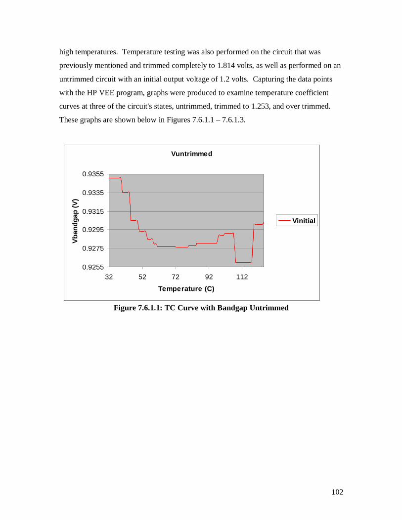
102
high temperatures. Temperature testing was also performed on the circuit that was
previously mentioned and trimmed completely to 1.814 volts, as well as performed on an
untrimmed circuit with an initial output voltage of 1.2 volts. Capturing the data points
with the HP VEE program, graphs were produced to examine temperature coefficient
curves at three of the circuit's states, untrimmed, trimmed to 1.253, and over trimmed.
These graphs are shown below in Figures 7.6.1.1 – 7.6.1.3.
Figure 7.6.1.1: TC Curve with Bandgap Untrimmed
Vuntrimmed
0.9255
0.9275
0.9295
0.9315
0.9335
0.9355
32 52 72 92 112
Temperature (C)
Vba
ndga
p (V
)
Vinitial

103
Figure 7.6.1.2: TC Curve with Bandgap Trimmed to 1.253V
Figure 7.6.1.3: TC Curve with Bandgap Over-trimmed
Vaccurate
1.2649
1.2654
1.2659
1.2664
1.2669
1.2674
1.2679
32 52 72 92 112
Temperature (C)
Vba
ndga
p (V
)
Vaccurate
Vover-trimmed
1.78
1.785
1.79
1.795
1.8
1.805
32 52 72 92 112
Temperature (C)
Vba
ndga
p (V
)
Vover

104
These curves show that for different Rt values, there will be a family of curves
that represent different operating points at different temperatures.
7.6.2 Voltage Supply Sweep
Following the test procedure, a voltage supply sweep test was done to verify
functionality of the bandgap circuit over a varying supply voltage. The supply voltage
was stepped from 0 volts to 5 volts in increments of 0.1 volt and VBADNGAP readings were
taken at each step. The results of this sweep are shown in Figure 7.6.2.1.
Figure 7.6.2.1: Output vs. Supply Variation
From this graph it can be seen that the bandgap voltage drops off rapidly around
3.9 volts. This is important because the voltage reference falls out of specifications,
which is supposed to be 3.0-volt minimum. After analyzing the problem, it was
determined there was a design flaw in the startup circuit. In the startup there is a 3.5-volt
bias being input to the gate of the startup PMOS transistor. It is also know that this
transistor also has a threshold voltage of -1.04 volts. Therefore, the transistor will dip
into the triode region and out of saturation once VDD drops lower than 3.96 volts.
Equations 7.6.2.1 and 7.6.2.2 must be satisfied for a PMOS transistor to be in saturation,
Output vs. Supply Variation
0.0000
0.1500
0.3000
0.4500
0.6000
0.7500
0.9000
1.0500
1.2000
0 1 2 3 4 5
Supply Voltage (V)
Out
put V
olta
ge (
V)

105
and when VDD falls below 3.96 in this circuit the first equation is no longer satisfied and
therefore the transistor is in the active region.
tGS VV ≤ (7.6.2.1)
tGSDS VVV −≤ (7.6.2.2)
For example, if VDD = 3.7 volts, then VGS will not be less than Vt, because VGS =
3.5V - 3.7V = -0.2V, which is greater than Vt or -1.04V. For that reason, when this
happens in this circuit the bandgap voltage will drop off immediately and cause power
supply rejection.
7.7 Test Circuit #2 (NPN)
At Allegro Microsystems, access was granted to use a laser trim station. Using this
station, it was possible to trim circuits 1 and 2, which were unreachable on the probe
station. Only the bandgap circuit with NPN transistors was trimmed at this time because
test data has already been obtained for a bandgap circuit with PNP devices.
To test circuit 2, the chip was powered up to 4.80V at 25ºC and trimmed according
to the trim procedure from Chapter 5. The NPN bandgap circuit was successfully
trimmed to 1.2501V and the trim results are shown in Table 7.7.1. A die photo of a link
cut with a laser can be seen in Appendix A.
Table 7.7.1: VBANDGAP vs. Rt
Links Cut (R t)Link
NumberResistance
Added VBANDGAP
Base (3.0k ohm) - - 0.9190Cut first link (1.065k ohm) 1 1.065K 1.1040
Cut second link 2 533.5 1.1970CoarseTrim
Cut third link 3 266 1.2425Cut sixth link 6 33.2 1.2490Fine
Trim Cut ninth link 9 4.6 1.2501
A temperature sweep of this trimmed circuit was done using the HP-VEE. Following the
test procedure, the chip was heated to 125 degrees Celsius and left to cool down to room
temperature. The curve produced is shown in Figure 7.7.1.

106
Figure 7.7.1: Measured Temperature Sweep of VBANDGAP vs. Temperature
This curve shows that VBANDGAP has a flat response over temperature and remains
equal to 1.250 with much less than 1-percent variation. This can be seen in above in
Figure 7.7.1, which shows the y axis boundaries to be plus one percent and minus one
percent of 1.250.
Similar results were obtained when trimming another circuit #2 on a different
chip. This circuit was also powered to 4.80V at 25ºC and trimmed using Allegro's laser
station. VBANDGAP in this circuit was trimmed to precisely 1.2500 volts and like the other
NPN circuit, remained constant, or flat, over a temperature sweep.
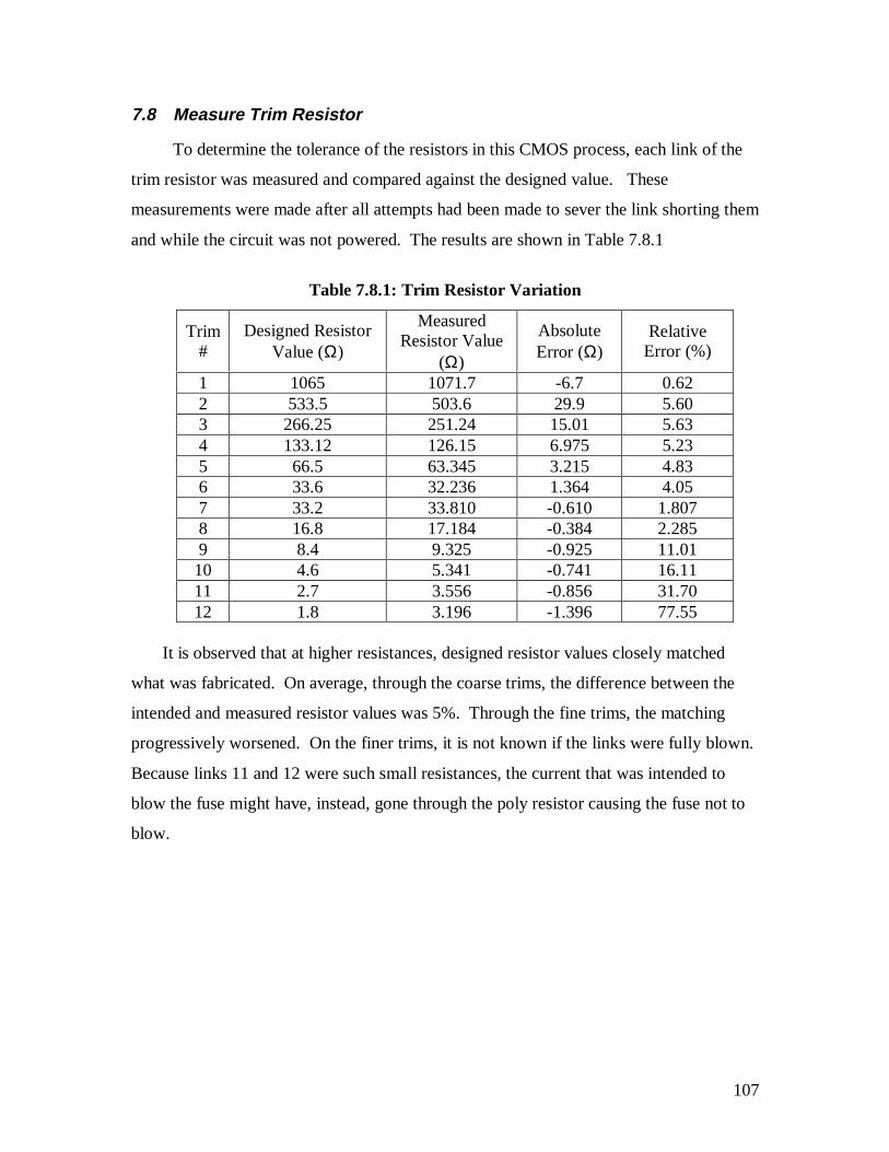
107
7.8 Measure Trim Resistor
To determine the tolerance of the resistors in this CMOS process, each link of the
trim resistor was measured and compared against the designed value. These
measurements were made after all attempts had been made to sever the link shorting them
and while the circuit was not powered. The results are shown in Table 7.8.1
Table 7.8.1: Trim Resistor Variation
Trim#
Designed ResistorValue (Ω)
MeasuredResistor Value
(Ω)
AbsoluteError (Ω)
RelativeError (%)
1 1065 1071.7 -6.7 0.622 533.5 503.6 29.9 5.603 266.25 251.24 15.01 5.634 133.12 126.15 6.975 5.235 66.5 63.345 3.215 4.836 33.6 32.236 1.364 4.057 33.2 33.810 -0.610 1.8078 16.8 17.184 -0.384 2.2859 8.4 9.325 -0.925 11.0110 4.6 5.341 -0.741 16.1111 2.7 3.556 -0.856 31.7012 1.8 3.196 -1.396 77.55
It is observed that at higher resistances, designed resistor values closely matched
what was fabricated. On average, through the coarse trims, the difference between the
intended and measured resistor values was 5%. Through the fine trims, the matching
progressively worsened. On the finer trims, it is not known if the links were fully blown.
Because links 11 and 12 were such small resistances, the current that was intended to
blow the fuse might have, instead, gone through the poly resistor causing the fuse not to
blow.

108
8 Conclusions and Recommendations
Overall the design of the bandgap voltage reference was a success. While not all of
the individual circuits worked as expected, it was possible to develop a voltage reference
accurate to ±1% using components that had a 20% tolerance and meet specifications.
Table 8.1 shows the revised specifications. This final specification sheet is representative
of the NPN bandgap circuit number two.
Table 8.1: Final Specification SheetMin. Typ. Max. Units
Output Voltage 1.2499 1.2500 1.2501 V
Maximum Tempco - - 40 PPM/°C
Initial Accuracy - - ±1 mV
Supply Voltage 3.9 5 5 V
Temperature Operating
Range
+25 - +125 °C
As stated in the chapter on results, the final results show the bandgap to operate at
a constant value over a temperature. Initial accuracy meets and exceeds the initial design
spec. The only spec not met completely is the minimum supply voltage that allows this
circuit to operate. This however was not a fatal error and recommendations are discussed
later in this chapter on ways to improve this result.
8.1 Overall Design
The layout of the design could have been optimized and compacted. For research
purposes this was not an issue, but if the design were to be incorporated into another
design at AllegroMicrosystmes, the die area should be used more carefully. Components
should be spaced closer together and trims on the trim scheme (the 1Ω and 2Ω trims for
example) could be removed since it was demonstrated that the extra resolution was not
needed.
109
8.2 Transistors in a CMOS Process
It was unclear as to what should be expected from the bipolar transistors made in a
CMOS process. Fortunately, they performed well, exhibiting characteristics normal to
true bipolar transistors.
However, the PNP transistors did not operate in the bandgap circuit as expected.
Upon initial powering and without any trims, the bandgap output voltage was designed to
produce approximately 900mV. Yet, the circuits with the PNP devices had an initial
voltage of approximately 1.23V.
This may be due to the improper sizing of the device. While the NPN transistor was
designed according to recommendations from MOSIS, there were no recommendations
for a PNP transistor. While it was intended to be a device with vertical current flow, due
to the small size of the base-emitter junction, there was also some lateral current flow.
This affected the overall β of the transistor and had the dimensions of the transistor been
increased, this effect may have disappeared and may have behaved properly.
These undesirable effects might also have been avoided through better simulations.
Because an accurate model for either bipolar transistor was non-existent, it was
impossible to fully predict how the device would operate. Otherwise, creating a PNP
transistor in a CMOS process is possible and should yield favorable results in the future.
8.3 Amplifier
The design of the operational transconductance amplifier was also a moderate
success. While the offset voltage and gain were not commendable, they were adequate
for this design. The output swing on the single supply amplifier was not rail to rail but
approximately from 0.7 to 3.5V. This should not affect correct circuit operation and a
stable reference is still achievable.
More space could have been devoted to the optimization of the amplifier because
there was extra area on the chip available. However, due to time constraints, this was not
done.
110
8.4 Trimming
While laser trimming appeared to be more destructive (see Figures A6, A7, & A8),
it could also save time and money as previously discussed. The laser output was not
adjusted in lab, but could have been modified to control the damage the laser induced.
Trimming of an individual circuit is definitely easier using a laser than a probe
station. With the probes, two pins must be aligned whereas with the laser, it is quite
simple to aim the crosshairs over the link and pulse the laser.
8.5 Trimming Consideration
It was also noticed that when trimming circuit 2 at Allegro, the light source from
the microscope had an adverse affect on the accuracy of the output of the bandgap
voltage. Even when the scope light was turned off, the ambient light from the room
affected the output voltage. To maintain the highest accuracy trim, the bandgap voltage
should be measured when the lid has been replaced over the cavity thereby sealing off as
much light as possible. Most likely, these effects are caused due to the construction of
the bipolar transistors. Because they were fabricated in a CMOS process, they are less
than ideal, and, as a photodiode would, allow light into the pn junctions, which generates
more carriers and alters the voltage drop across the base-emitter junctions.
8.6 Recommendation for Start Up Circuit
The start-up circuit performed as needed by creating a differential at the inputs of
the first amplifier upon power-up. However, a different design should be implemented in
the future. As the supply voltage dropped, the PMOS transistor entered the triode region
resulting in the loss of one quarter of the total current available to the bipolar transistors.
With less current available to the bipolar transistors than designed, the bandgap output
voltage dropped as was seen in the graphical output in Chapter 7.7. An improvement to
the design may call for a resizing of the device, but that would only lessen the effect and
not cancel it completely. Another solution would be to provide a voltage less than the
current a 3.5 volt bias that is being input to the gate of the transistor currently. In which
case a lower supply voltage could be reached without falling out of specifications.

111
References
ASM International Handbook Committee. Packaging. Electronic Materials Handbook,
Vol. 1, 1989, p. 462-468.
Brokaw, A. P. A Simple Three-Terminal IC Bandgap Reference, IEEE Journal of Solid-
State Circuits, Vol. SC-9, p 388-393, December 1974.
Chao, Robert. Trimming analog circuits with solid-state devices. The Practical
Engineer, 1997.
Gray, Paul, Meyer, Robert, Analysis and Design of Analog Integrated Circuits, 3rd Ed.,
1977.
Gunawan, Made, Meijer, Gerard C. M., Fonderie, Jeroen, Huijsing, Johan H., A
Curvature-Corrected Low-Voltage Bandgap Reference, IEEE Journal of Solid-State
Circuits, Vol. SC-28, No. 6, p 667-670, June 1993.
Hamer, D. W., Biggers, J. V. Laser Trimming. Thick Film Hybrid Microcircuit
Technology, 1972, p. 187-190.
Horowitz, Paul, Hill, Winfield The Art of Electronics, 2nd Ed., 1989
Kuijk, Karel E. A Precision Voltage Source, IEEE Journal of Solid-State Circuits, Vol.
SC-8, No. 3, p 222-226, June 1973.
Licari, James J., Enlow, Leonard R. Resistor Trimming. Hybrid Microcircuit
Technology Handbook, 1988, p. 132-148.
Michejda, John, Kim, Suk. K. A Precision CMOS Bandgap Reference, IEEE Journal of
Solid-State Circuits, Vol. SC-19, no. 6, p 1014-1021, December 1984.
Pierret, Robert F. Semiconductor Device Fundamentals, 1st Ed., 1996.
Pritchard, R. L. Electrical Characteristics of Transistors, 1st Ed., 1967.
Riddle, Robert L., Ristenbatt, Marlin P. Transistor Physics and Circuits, 1st Ed., 1958.
Sedra, Adel S., Smith, Kenneth C. Microelectronic Circuits, 4th Ed., 1991.
Song, Bang-Sup, Gray, Paul R. A Precision Curvature-Corrected CMOS Bandgap
Reference, IEEE Journal of Solid-State Circuits, Vol. SC-18, no. 6, p 634-643, December
1983.

112
Widlar, R. J. New Developments in IC Voltage Regulators, IEEE Journal of Solid-State
Circuits, Vol. SC-6, p 2-7, February 1971.
Wong, James, Voltage References for High Accuracy Systems, Analog Devices
Databook, Section 5.
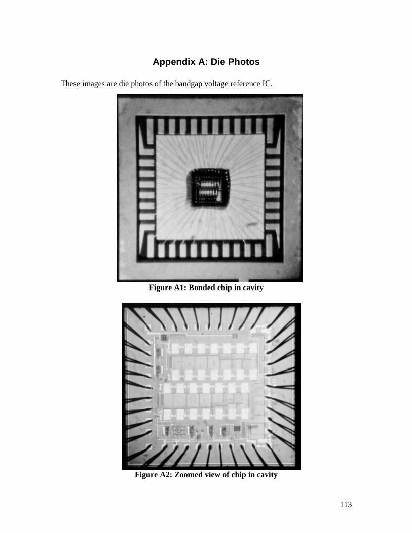
113
Appendix A: Die Photos
These images are die photos of the bandgap voltage reference IC.
Figure A1: Bonded chip in cavity
Figure A2: Zoomed view of chip in cavity

114
Figure A3: Thermal Image of an Amplifier at 281X
Figure A4: Another image of an amplifier at 400X

115
Figure A5: Intact link fuses at 200X
Figure A6: Links blown using power supply at 200X

116
Figure A7: Links cut with a laser at 200X
Figure A8: Link completely cut with laser at 281X
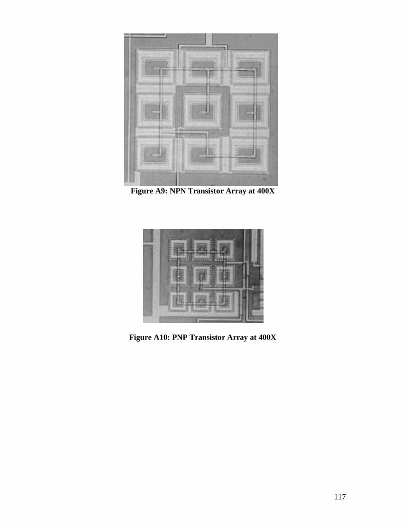
117
Figure A9: NPN Transistor Array at 400X
Figure A10: PNP Transistor Array at 400X

118
Appendix B: Glossary and Acronyms
Acronyms:
BJT: Bipolar Junction TransistorCMOS: Complementary Metal Oxide SemiconductorCTAT: Complementary to Absolute TemperatureMOSFET: Metal Oxide Semiconductor Field Effect TransistorMOSIS: MOS Implementation Service in Marina del Rey CANMOS: N-Channel MOSFETPMOS: P-Channel MOSFETPTAT: Proportional to Absolute TemperatureTempco: Temperature Co-efficient
Glossary:
BandgapVoltage:
For silicon, 1.205V; the base-emitter voltage of bipolar transistor at0º Kelvin
Beam speed: A measure of the speed at which resistive material is removed, inchesper second. Similar to Cut Speed and Table Speed.
Bite size: The amount of additional material attacked with each laser pulse.Cut Speed: A measure of the speed at which resistive material is removed, inches
per second. Similar to Beam Speed and Table Speed.Hole size: Diameter of the area of resistive material removed. The diameter of the
hole is related to the optical spot size, but is not necessarily the same.It varies with the material being cut and the power level of the laserpulse.
Kerf width: The outer width of the cut.Q-Rate: The number of laser pulses issued per second.
Spot size: Diameter of the material removed. The diameter of the hole is relatedto the optical spot size, but is not necessarily the same. It varies withthe material being cut and the power level of the laser pulse.
Table speed: The rate of resistive material removed in inches per second.
TemperatureCoefficient:
A constant representing a change in voltage per degree Celsius;Tempco

119
Appendix C: Fundamental Principles of Bipolar JunctionTransistors
Bipolar Junction Transistors
This appendix provides the basics for understanding the fundamental operations of
bipolar junction transistors.
Transistor Fundamentals
A bipolar junction transistor is created from a single crystal, most commonly
silicon or germanium, that contains both N-type and P-type diffused regions. The N-type
and P-type regions are doped segments of intrinsic silicon that have had specific
impurities injected in it depending on the desired polarity. The impurities are chosen
because after the injection there are free mobile electrons or holes in the lattice of the
crystal. In the N-type silicon, the number of mobile electrons (ND) vastly outnumbers the
number of mobile holes (NA). Conversely, the opposite is true for P-type silicon.
For a bipolar junction transistor, it is required that two P-type and N-type regions
are back-to-back in a single crystal because electrons and holes can freely propagate
throughout the crystal’s lattice. Thus there are only three regions in a single transistor;
either a P-type region is sandwiched between two N-type regions creating an NPN
transistor or, conversely, an N-type region is enclosed between two P-type regions
making a PNP transistor.

120
N P
P N
N P
Figure 2.4: Transistor regions for a) NPN and b) PNP
types
Inherently, without any external voltage being applied, biases develop when the
two junctions are created beside one another. To counteract these biases to allow current
to flow, external voltages must be applied to the transistor. The emitter of the transistor
is defined as the PN junction that has a forward bias applied to it and the collector is
defined as the PN junction that has a reverse-bias applied to it. The base of the transistor
is the region in the middle of the transistor.
With the proper biases applied and connections made, the bipolar junction
transistor acts as a current amplifier with the base acting as the input. Very small
currents (on the order of nano-amperes) can control currents that are orders of
magnitudes larger, making the transistor an effective current-controlled device. The
transistor can also be connected in a diode configuration in which, for a NPN transistor,
the collector is connected to the base. This is useful in certain applications, which will be
detailed later.
Transistor Currents
The most important current in the transistor is in its base. For this analysis, NPN
type transistors will be used as the example. Because the emitter is forward biased, it
emits electrons into the base region. Once received in the base region, the electrons are
considered the minority carrier since, in P-type regions, the number of holes is much
greater then the number of electrons. Because of the polarities of having two PN
junctions back-to-back, there is no electric field in the base of the transistor leaving the
electrons free to move by the process of diffusion. Once the electrons scatter within a
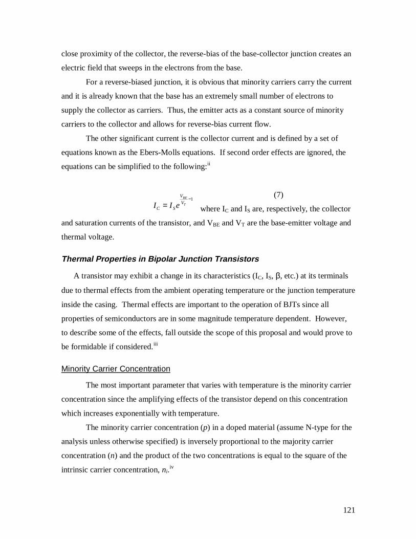
121
close proximity of the collector, the reverse-bias of the base-collector junction creates an
electric field that sweeps in the electrons from the base.
For a reverse-biased junction, it is obvious that minority carriers carry the current
and it is already known that the base has an extremely small number of electrons to
supply the collector as carriers. Thus, the emitter acts as a constant source of minority
carriers to the collector and allows for reverse-bias current flow.
The other significant current is the collector current and is defined by a set of
equations known as the Ebers-Molls equations. If second order effects are ignored, the
equations can be simplified to the following:ii
(7)
where IC and IS are, respectively, the collector
and saturation currents of the transistor, and VBE and VT are the base-emitter voltage and
thermal voltage.
Thermal Properties in Bipolar Junction Transistors
A transistor may exhibit a change in its characteristics (IC, IS, β, etc.) at its terminals
due to thermal effects from the ambient operating temperature or the junction temperature
inside the casing. Thermal effects are important to the operation of BJTs since all
properties of semiconductors are in some magnitude temperature dependent. However,
to describe some of the effects, fall outside the scope of this proposal and would prove to
be formidable if considered.iii
Minority Carrier Concentration
The most important parameter that varies with temperature is the minority carrier
concentration since the amplifying effects of the transistor depend on this concentration
which increases exponentially with temperature.
The minority carrier concentration (p) in a doped material (assume N-type for the
analysis unless otherwise specified) is inversely proportional to the majority carrier
concentration (n) and the product of the two concentrations is equal to the square of the
intrinsic carrier concentration, ni.iv
1−= T
BE
V
V
SC eII

122
pn = ni2 (8)
Because intrinsic, or pure, silicon has no net charge, the number of electrons
equals the number of holes which, in turn, also equals the intrinsic carrier concentration
from Equation 7. For correct operation of the transistor, however, it is necessary for
there to be a significant difference between the quantity of majority and minority carriers
in the silicon.
After further manipulation of (7) and the application of selected principles of
quantum mechanics, it can be shown that v
kTEEC
FCeNn /)( −−= (9)
kTEEV
VFeNp /)( −−= (10)
where NC and NV are the number of electrons and holes in the conduction and valence
states, respectively. (EC-EF) and (EV-EF) represent the energy differences between the
conduction band and Fermi level and the valence band and Fermi level. k is Boltzmann’s
constant and T is temperature in degrees Kelvin.
The Fermi level is a reference energy level from which all energies may be
conveniently measured, and furthermore, it “can be defined as that energy at which the
probability of finding an electron n energy units above the level is equal to the probability
of finding an “absence” of an electron [or hole] n energy units below the level.”vi The
Fermi level is, in intrinsic silicon, considered to halfway between the valence and
conduction energy bands of charged particles. When silicon is of N-type, the Fermi level
is shifted towards the conduction band due to the increase in the number of electrons and,
conversely, when the silicon is of P-type, the Fermi level shifts towards the valence band
due to the abundance of holes. It is also known that at high temperatures, the Fermi level
shifts towards the center between the valence and conduction bands, that is, it returns to a
state of equilibrium equidistant from each band.
123
It is now obvious that to calculate the intrinsic carrier concentration, it is possible
to substitute Equations (8) and (9) into (7) to determine the concentration in terms of the
relative position of the Fermi level, and thusvii
kTEii
GeTKn /32 −= (11)
where Ki is equal to a combination of ratios involving relative effective masses,
Boltzmann’s constant, and other miscellaneous constants common in quantum
mechanics. For our purposes, Ki is estimated as 1.5 x 1045 for silicon. EG is the energy
gap difference between the conductance bands and valence bands. The Fermi levels, EF,
cancel out of the equation when the substitution occurs. It is suggested that, for silicon,
1.16 electron volts be used for EG however a disclaimer is included that 1.16eV is an
average between a ‘normally quoted value’ and the calculated value from the
derivation.viii
Thus, for intrinsic silicon, the minority carrier concentration dependence on
temperature can be calculated and resulting in the following equation.ix
kTEii
GTKnpn 2/23
21 −=== ε (12)
If the silicon is doped (for N-type) then the minority-carrier (hole) concentration
can be found be again manipulating Equation (7) to result inx
kTE
AD
i
AD
i GeTNN
K
NN
np /3
2−
−=
−= (13)
while the majority carrier concentration is still the difference between the number of
donors and acceptors (for N-type).
As the temperature increases, it is easy to see the minority carrier-concentration is
directly proportional to the cube of temperature, which will dominate and drive the
number of minority carriers to infinity. Of course, as with all exponential functions, there
are limits to the system and this behavior cannot continue forever. There are a finite
number of holes that can be generated from the impurities injected into the silicon before
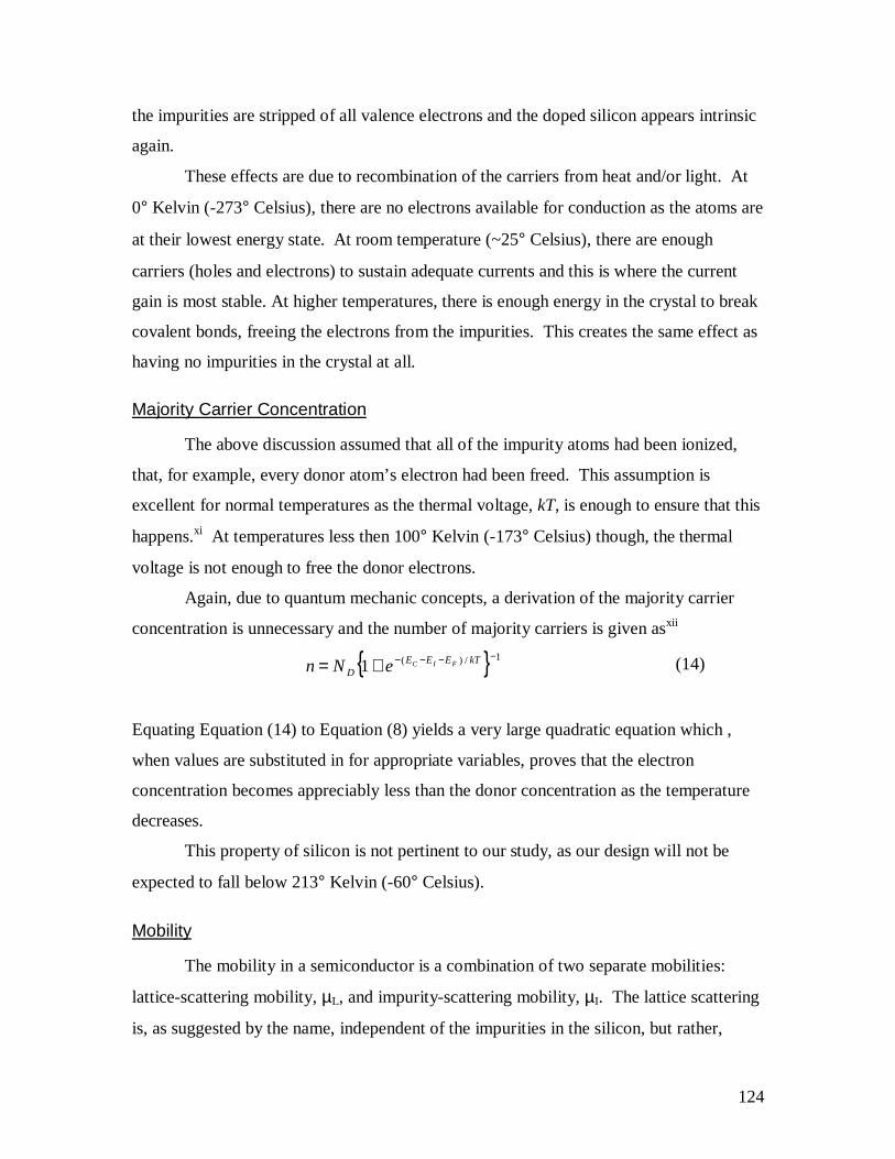
124
the impurities are stripped of all valence electrons and the doped silicon appears intrinsic
again.
These effects are due to recombination of the carriers from heat and/or light. At
0° Kelvin (-273° Celsius), there are no electrons available for conduction as the atoms are
at their lowest energy state. At room temperature (~25° Celsius), there are enough
carriers (holes and electrons) to sustain adequate currents and this is where the current
gain is most stable. At higher temperatures, there is enough energy in the crystal to break
covalent bonds, freeing the electrons from the impurities. This creates the same effect as
having no impurities in the crystal at all.
Majority Carrier Concentration
The above discussion assumed that all of the impurity atoms had been ionized,
that, for example, every donor atom’s electron had been freed. This assumption is
excellent for normal temperatures as the thermal voltage, kT, is enough to ensure that this
happens.xi At temperatures less then 100° Kelvin (-173° Celsius) though, the thermal
voltage is not enough to free the donor electrons.
Again, due to quantum mechanic concepts, a derivation of the majority carrier
concentration is unnecessary and the number of majority carriers is given asxii
1/)(1−−−−+= kTEEE
DFICeNn (14)
Equating Equation (14) to Equation (8) yields a very large quadratic equation which ,
when values are substituted in for appropriate variables, proves that the electron
concentration becomes appreciably less than the donor concentration as the temperature
decreases.
This property of silicon is not pertinent to our study, as our design will not be
expected to fall below 213° Kelvin (-60° Celsius).
Mobility
The mobility in a semiconductor is a combination of two separate mobilities:
lattice-scattering mobility, µL, and impurity-scattering mobility, µI. The lattice scattering
is, as suggested by the name, independent of the impurities in the silicon, but rather,

125
dependent on the crystal lattice structure of the silicon. The impurity-scattering mobility
is dependent on the concentration of impurities injected and decreases inversely as
impurity density increases. Thus, the total mobility of the carriers in a transistor is the
sum of both mobilities. At room temperatures, the lattice scattering mobility is much less
than the impurity scattering mobility, thus the overall mobility is determined by the
impurity scattering mobility. With increasing impurity concentration however, the roles
have switched. Because of the difference in temperature dependence in both mobilities,
the overall mobility tends to stay the same over a wide range of temperatures.
It is also seen that as the temperature increases, the base of the transistor widens.
As the base widens, the electrons must travel a greater distance from the emitter to the
collector.xiii This increases the likelihood that not all electrons will get swept into the
collector after first being discharged from the emitter. Depending upon the lattice-
scattering, this delay may be significant enough to slow the response of the transistor.
Conductivity
The concepts of conductivity have already been briefly touched upon and only in
extreme cases when the transistor is heated to excessive temperatures do the electrons
break free of the impurity atoms causing the silicon to essentially become intrinsic. This
of course, increases the resistivity, the inverse of conductivity, of the transistor's
junctions.
Other Factors
Other properties discussed include the diffusion constant and the lifetime of the
transistor. The diffusion constant relates the frequency response of the transistor to the
heat applied to the unit. However, the temperature effect is negligible. Also, the lifetime
of a transistor as it is effected by heat is a complex analysis and is not easily predicted.xiv

126
Thermal Effects in Bipolar Junction Transistors
Saturation Current
The saturation current, or reverse leakage current, of a transistor is the most heat-
sensitive parameter. The junction current is given asxv
[ ]1/ −= kTVqS
eeII (15)
where the saturation current IS is equal toxvi
+=
n
pn
p
np
eS
nDpDSqI
λλ00
(16)
and Dp, Dn are the diffusion rates for holes and electrons, lp, ln are the thicknesses of the
N and P regions, S is the sensitivity, and pn0 and np0 are the minority carrier
concentrations. It is shown that the transistor saturates at lower threshold voltages as the
temperature increases and that a smaller forward bias is required.xvii
After a lengthy derivation, it is proven that the saturation current (in a germanium
transistor) doubles for every 8° Celsius and increases an order of magnitude every 25°
Celsius increase. Data for silicon transistors was unavailable but the increase in
saturation current is more rapid due to the higher energy gap of silicon.
Transistor Current Gain βF
The temperature dramatically affects the forward gain of a transistor, βF, due to
the extremely high doping density of the emitter. At higher collector currents (larger than
1 mA), it is difficult to achieve a gain greater than 200. At 100µA, the temperature will
provide a relatively constant gain for a constant collector current over a range of 50uA to

127
500uA. At room temperature (~25° Celsius), there are enough carriers (holes and
electrons) to sustain adequate currents and this is where the current gain is the most
stable. As the temperature decreases from 125° Celsius to -55° Celsius, the maximum
gain of the transistor is decreased. This is most likely due to the higher number of
minority carriers available at higher temperatures and the intrinsic properties of silicon.
Collector Characteristics
The collector current itself also varies with temperature as seen from Equation 1,
the Ebers-Molls equation, since VT, the thermal voltage, is directly proportion to the
temperature. It would also appear that the VBE in the Ebers-Molls equation would have a
positive temperature coefficient. However, due to the temperature dependence of the
saturation current, IS, the base-emitter voltage actually decreases 2.1 mV per degree
Celsius, or is approximately equal to the inverse of the absolute temperature.xviii
Because of the temperature characteristics of the transistor, the operating point
and characteristics of the transistor deviate greatly. It is shown that when the temperature
varies slightly, a plot of VCE versus IC (describing the collector characteristics) shifts
upward yet the spacing between the curves, determined by the base current, remains the
same.xix Thus the bias current depends on the temperature whereas the collector-to-
emitter voltage does not.
Also, when a load line is placed across the plots, it can be seen that the operating point of
the transistor varies with the temperature. The allowable swing for the collector current
(for increasing base currents) has been greatly reduced.xx It can also be seen that as the
temperature increases indefinitely, the operating point will eventually lie on the y-axis, or
the operating point would be equal to the collector current, IC.

128
i 1998-1999 Undergraduate Catalog, WPI, page 36.
ii The Art of Electronics, Cambridge University Press, Paul Horowitz, Winfield Hill, p. 80, c. 1989iii Electrical Characteristics of Transistors, McGraw-Hill, Inc., R.L. Pritchard, Toronto, p. 576, c1967iv Ibid., p 577.v Ibid., p 580.vi Transistor Physics and Circuits, page 36.vii Electrical Characteristics of Transistors, p 581.viii Ibid., p 581.ix Ibid., p 581.x Ibid., p 582.xi Ibid., p 582.xii Ibid., p 582.xiii Transistor Physics and Circuits, page 48.xiv Electrical Characteristics of Transistors, p 590.xv Ibid., p 593.xvi Ibid., p 594.xvii Ibid., p 594.xviii The Art of Electronics, page 81.xix Transistor Physics and Circuits, page 268.xx Ibid., page 270.