Plasma Etching a Ceramic Composite - NASA Etching a Ceramic Composite ... (Si3N4) 1 glass, and...
13
y :;V,7,Az" 4F y,6 NASA Technical Memorandum 105430 Plasma Etching a Ceramic Composite David R. Hull National Aeronautics and Space Administration Lewis Research Center Cleveland, Ohio Todd A. Leonhardt Sverdrup Technology, Inc. Lewis Research Center Group Brook Park, Ohio and William A. Sanders Analex Corporation Brook Park, Ohio Prepared for the 24th Annual Convention of the International Metallographic Society Monterey, California, July 29—August 1, 1991 NASA https://ntrs.nasa.gov/search.jsp?R=19920013062 2018-06-02T15:57:14+00:00Z
Transcript of Plasma Etching a Ceramic Composite - NASA Etching a Ceramic Composite ... (Si3N4) 1 glass, and...

y :;V,7,Az"4F y,6
NASA Technical Memorandum 105430
Plasma Etching a Ceramic Composite
David R. HullNational Aeronautics and Space AdministrationLewis Research CenterCleveland, Ohio
Todd A. LeonhardtSverdrup Technology, Inc.Lewis Research Center GroupBrook Park, Ohio
and
William A. SandersAnalex CorporationBrook Park, Ohio
Prepared for the24th Annual Convention of the InternationalMetallographic SocietyMonterey, California, July 29—August 1, 1991
NASA
https://ntrs.nasa.gov/search.jsp?R=19920013062 2018-06-02T15:57:14+00:00Z

maom
PLASMA ETCHING A CERAMIC COMPOSITE
David R. HullNational Aeronautics and Space Administration
Lewis Research CenterCleveland, Ohio 44135
Todd A. LeonhardtSverdrup Technology, Inc.
Lewis Research Center GroupBrook Park, Ohio 44142
and
William A. SandersAnalex Corporation
3001 Aerospace ParkwayBrook Park, Ohio 44142
SUMMARY
Plasma etching is found to be a superior metallographic technique for evaluating the micro-structure of a ceramic matrix composite. The ceramic composite studied is composed of siliconcarbide whiskers (SiC W) in a matrix of silicon nitride (Si 3N4 ) 1 glass, and pores. All four con-stituents are important in evaluating the microstructure of the composite. Conventionally pre-pared samples, both as-polished or polished and etched with molten salt, do not allow all fourconstituerits to be observed in one specimen. As-polished specimens allow examination of theglass phase and porosity, while molten salt etching reveals the Si 3 N4 grain size by removing theglass phase. However, the latter obscures the original porosity. Neither technique allows theSiCW to be distinguished from the Si 3 N4 . Plasma etching with CF 4 +4%02 selectively attacksthe Si 3N4 grains, leaving the SiC W and glass in relief, while not disturbing the pores. An artifactof the plasma etching reaction is the deposition of a thin layer of carbon on Si 3 N4 , allowingSi3N 4 grains to be distinguished from SiC W by back scattered electron imaging.
INTRODUCTION
The need for more efficient propulsion systems requires materials to operate at increasinglyhigher temperatures in oxidizing environments. Ceramics are a leading candidate to providehigh temperature strength and oxidation resistance. A major problem with ceramics is their lowfracture toughness, which leads to brittle catastrophic failures. A method of increasing thetoughness has been to introduce interfaces to deflect a propagating crack. One material systembeing studied is a ceramic composite composed of SiC W in a matrix of Si3N4 . The SiCW providethe interfaces to deflect the crack tip (ref. 1).
The fabrication of SiC W/Si3N4 matrix composites involves several variables; i.e., whiskermorphology and volume fraction, glass composition and volume fraction, consolidation tempera-ture and pressure. Metallography plays a critical role in the evaluation of the effects of thesevariables on the composite. Metallography provides the ability to observe porosity, Si3N4 grainand SiCW size, percent glass and distribution of the phases. Correlation of microstructural

information with mechanical property data can be used to modify fabrication processes tofurther improve mechanical properties.
In metallography, etching is the critical step in revealing a material's microstructure. Etch-ing is performed by selective removal of material from a specimen by a chemical reaction. Dif-ferent features in the microstructure react at different rates, providing topographic reliefobservable by optical and electron microscopy (ref. 2). An etchant commonly used on Si 3N 4 hasbeen molten salts (e.g., potassium hydroxide, KOH, used at 673 K). The molten salt dissolvesthe intergranular glass phase that surrounds each Si 3 N 4 grain, allowing the grains to beobserved.
Plasma etching is a dry etching technique developed for the fabrication of microelectronicsin the late 1960's (refs. 4 to 7). The technique uses an electric discharge excited by a radio fre-quency source to produce chemically reactive fragments from an appropriate gas in a vacuum of0.001 to 2 torr. The fragments react with the specimen creating volatile products which arepumped away. For silicon based materials the gas used is CF 4 , which breaks down to CFX andreacts with Si to form SiF y (gas) (ref. 4).
The use of plasma etching for revealing the microstructure of a sialon was first reported in1983 (ref. 8). Since then, others have used plasma etching to reveal the microstructure of Si3N4(refs. 9 to 11). In these materials, the #-sialon or Si3 N 4 are selectively removed, with the glassphase remaining in relief, thus revealing the microstructure. Only one reference was found onplasma etching a ceramic composite (Sic/Si 3N4) ( ref. 13). Plasma etching was used to removeSi3 N4 , thereby isolating the glass phase for chemical analysis in the transmission electron micro-scope (TEM). The purpose of this paper is to evaluate the use of plasma etching in revealingthe microstructure of a SiC W/Si3 N 4 matrix composite by examination in the scanning electronmicroscope (SEM).
EXPERIMENTAL
The SiCW /Si3N4 composite used for the plasma etching studies was formulated to yield afully dense composite containing 10 percent SiC W and 14 percent glass by volume. PremilledSi3N4 powder was blended in hexane with SiCW , and Ce 2 O3/S'02 sintering aid. The homoge-neous blended slurry was then pressed into a 5.1-cm diameter by 0.7 cm thick disk which wasdried, and then sintered at 2413 K for 4 hr under 2.5 MPa nitrogen overpressure. The bulkdensity of the disk was 3.31 g/cm 3 (immersion method. The disk was then sectioned to providespecimens for the plasma etching studies.
Metallographic preparation consisted of mounting the specimen in a two part epoxy, fol-lowed by vacuum degassing, and curing for 12 hr. The subsequent grinding/ polishing steps thatwere used are listed in table I.
Etching of the specimens was performed by two methods; molten salt or plasma etching.Etching with molten KOH was performed as outlined in figure 1. The specimen was removedfrom the epoxy mount, wrapped in platinum wire and immersed in molten KOH at 673 K for10 to 15 sec. Plasma etching was performed using the system shown in figure 2. The mountedsample is placed in the vacuum chamber and evacuated to 0.1 torr. The sample is preheatedusing nitrogen at 0.2 torr and plasma RF power of 100 W for 10 min. Next, etching is per-formed using CF 4+4%0 2 at 0.3 torr and plasma RF power of 100 W for 2 to 5 min.
2

Specimens were sputter coated with palladium and examined in a SEM using back scatteredelectron imaging and an accelerating voltage of 20 kV. TEM specimens were prepared by con-ventional techniques. A 3 mm disk was ultrasonically drilled from a 0.5 mm thick section,ground on both surfaces with 15 and 3 pm diamond to a thickness of 140 µm, and dimpled fromeach side to a thickness of less than 20 pm. Final thinning was performed by ion milling to per-foration using argon at 5 kV and 12° incidence angle. Electrical conductivity of the specimenwas achieved by evaporation of approximately 10 nm of carbon onto one surface. The specimenwas examined in the TEM at an accelerating voltage of 120 kV. After examination in the TEM,the specimen was affixed to a glass slide with small drop of carbon paint and plasma etched asdescribed above, with a preheat of 5 min and an etch of 2 min. The specimen was removed fromthe glass slide and re-examined in the TEM. Electron energy loss spectroscopy (EELS) was per-formed to obtain chemical information.
RESULTS
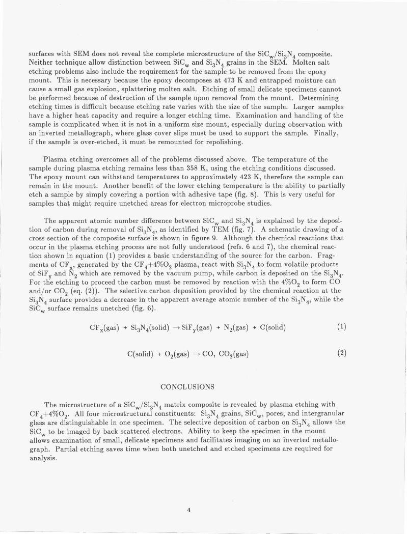
Back scattered electron imaging of the as-polished composite allows the identification ofthree microstructural features (fig. 3). The white phase is the CeO 2 rich glass phase as deter-mined by x-ray energy dispersive spectroscopy (XEDS), the black areas are regions of porosity,and the gray phase is SiC W or Si3 N4 . Measurement of the size and shape of the gray phase ispossible, but SiC W and Si3 N4 can not be differentiated due to their identical average atomicnumber (SiC:(14+6)/2=10; Si3N4:(3 *14+4*7)/7=10).
Molten salt etching removes the intergranular glass leaving the SiC W and Si3 N4 grains inrelief (fig. 4). Back scattered electron imaging again can not differentiate SiC W from Si3 N 4 . Thewhite particles were identified by XEDS as contamination from the platinum crucible duringetching. Obtaining reproducible etching results is difficult as shown by the influence an addi-tional 5 sec had on the depth of etching on a second specimen (fig. 4(b)).
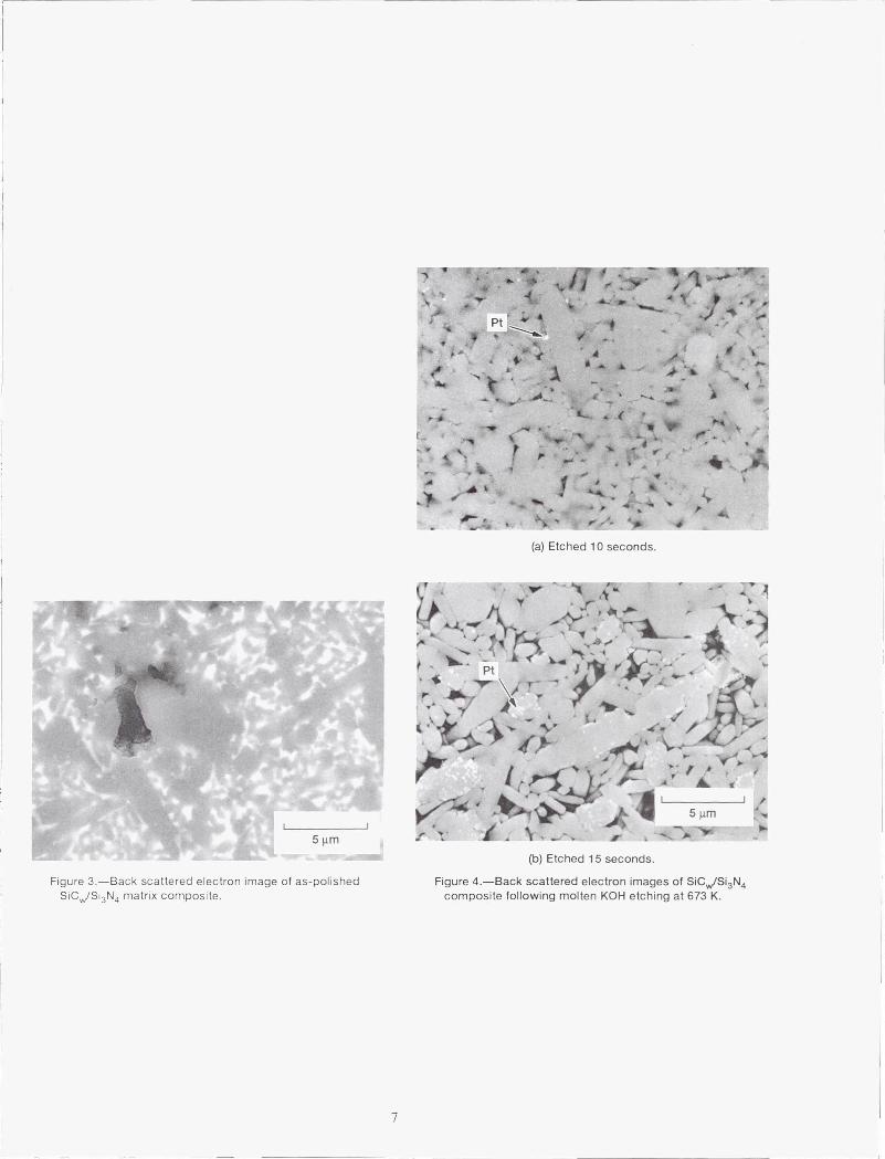
Plasma etching selectively attacks the Si 3 N 4 leaving the SiCW and glass in relief (fig. 5).Back scattered electron imaging reveals the CeO 2 rich glass as the white phase. An atomicnumber difference between Si 3 N4 and SiCW is observed, with the SiCW being lighter, and thus,apparently higher in average atomic number. As etching time is increased to 5 min, the contrastbetween SiC W and Si3 N 4 increases (fig. 5(b)). Examination of the specimen surfaces at highermagnification, using secondary electrons, reveals a mottled structure on the Si 3N4 , with the SiCWand glass appearing unaffected (fig. 6). The longer etching time (5 min) removed more of theSi3N4.
TEM of an as prepared specimen shows the typical faulted structure of the SiC W , an inter-granular glass phase, and Si3N4 grains containing dislocations (fig. 7(a)). After plasma etchingfor 2 min, examination of the exact same region shows the SiCW and glass are intact, but theSi3 N4 is removed as evidenced by the absence of the dislocations (fig. 7(b)). The evaporatedconductive carbon film is intact with a mottled deposit on it. Electron diffraction of the depositshowed an amorphous pattern and EELS shows carbon as the only element present (fig. 7(c)).
DISCUSSION
Many problems exist with the conventional microstructural characterization techniquesapplied to SiC W /Si3 N4 composites. Examination of both as-polished and molten salt-etched
3
surfaces with SEM does not reveal the complete microstructure of the SiC N,/Si3 N4 composite.Neither technique allow distinction between SiC W and Si 3 N 4 grains in the SEM. Molten saltetching problems also include the requirement for the sample to be removed from the epoxymount. This is necessary because the epoxy decomposes at 473 K and entrapped moisture cancause a small gas explosion, splattering molten salt. Etching of small delicate specimens cannotbe performed because of destruction of the sample upon removal from the mount. Determiningetching times is difficult because etching rate varies with the size of the sample. Larger sampleshave a higher heat capacity and require a longer etching time. Examination and handling of thesample is complicated when it is not in a uniform size mount, especially during observation withan inverted metallograph, where glass cover slips must be used to support the sample. Finally,if the sample is over-etched, it must be remounted for repolishing.
Plasma etching overcomes all of the problems discussed above. The temperature of thesample during plasma etching remains less than 358 K, using the etching conditions discussed.The epoxy mount can withstand temperatures to approximately 423 K, therefore the sample canremain in the mount. Another benefit of the lower etching temperature is the ability to partiallyetch a sample by simply covering a portion with adhesive tape (fig. 8). This is very useful forsamples that might require unetched areas for electron microprobe studies.
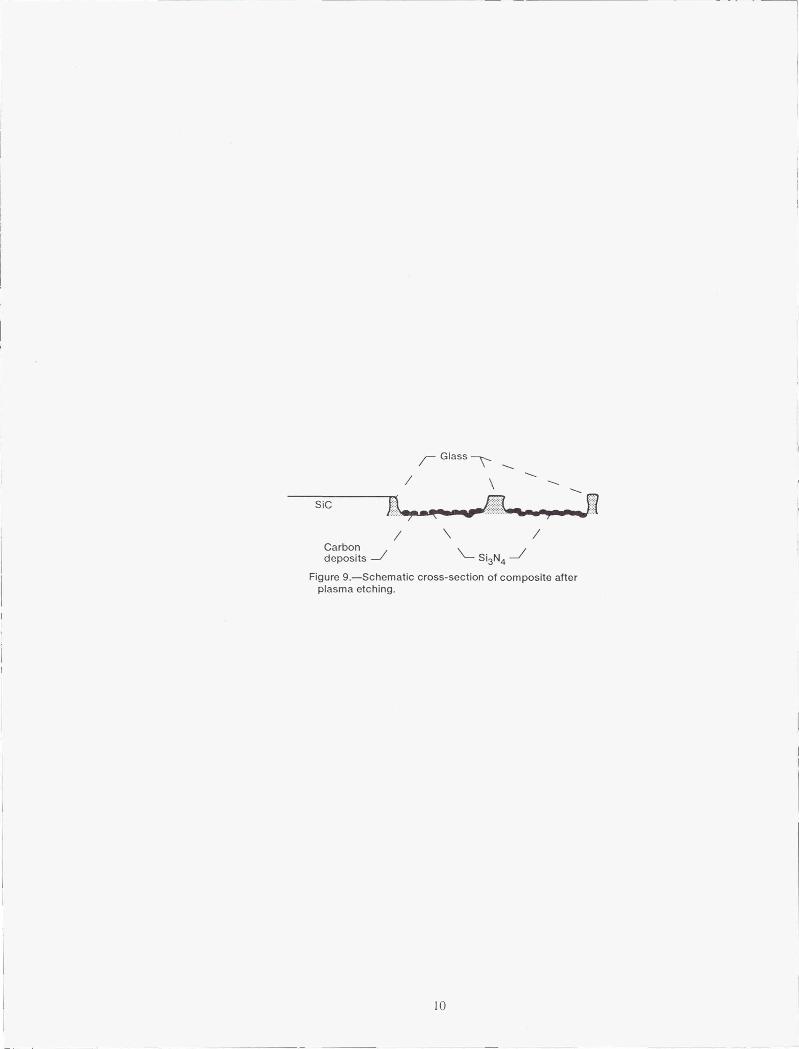
The apparent atomic number difference between SiC W and Si3 N4 is explained by the deposi-tion of carbon during removal of Si 3 N 4 , as identified by TEM (fig. 7). A schematic drawing of across section of the composite surface is shown in figure 9. Although the chemical reactions thatoccur in the plasma etching process are not fully understood (refs. 6 and 7), the chemical reac-tion shown in equation (1) provides a basic understanding of the source for the carbon. Frag-ments of CF x, generated by the CF 4+4%02 plasma, react with Si 3 N4 to form volatile productsof SiF and N 2 which are removed by the vacuum pump, while carbon is deposited on the Si3N4.For the etching to proceed the carbon must be removed by reaction with the 4%0 2 to form COand/or CO 2 (eq. (2)). The selective carbon deposition provided by the chemical reaction at theSi3 N 4 surface provides a decrease in the apparent average atomic number of the Si 3N4 , while theSiCW surface remains unetched (fig. 6).
CF x(gas) + Si3N 4(solid) —> SiF y (gas) + N 2 (gas) + C(solid) (1)
C(solid) + 0 2 (gas) —> CO, CO 2 (gas) (2)
CONCLUSIONS
The microstructure of a SiC w/Si3 N 4 matrix composite is revealed by plasma etching withCF 4+4%0 2 . All four microstructural constituents: Si 3 N 4 grains, SiCw , pores, and intergranularglass are distinguishable in one specimen. The selective deposition of carbon on Si 3N4 allows theSiCW to be imaged by back scattered electrons. Ability to keep the specimen in the mountallows examination of small, delicate specimens and facilitates imaging on an inverted metallo-graph. Partial etching saves time when both unetched and etched specimens are required foranalysis.

REFERENCES
1. Evans, A.G.: Perspective on the Development of High-Toughness Ceramics. J. Am. Ceram.Soc., vol. 73, no. 2, Feb 1990, pp. 187-206.
2. Kehl, G.A.: The Principles of Metallographic Laboratory Practice. McGraw-Hill, 1949.
3. Lange, F.F.: Relation Between Strength, Fracture Energy, and Microstructure of Hot-Pressed Si 3N4 . J. Am. Ceram. Soc., vol. 56, no. 10, 1973, pp. 518-522.
4. Bersin, R.: A Survey of Plasma Etching Processes. Solid State Technol., vol. 19, no. 5,1976, pp. 31-36.
5. Wolf, E.D.; Adesida, I.; and Chinn, J.D.: Dry Etching for Submicron Structures. J. Vac.Sci. Technol. A, vol. 2, no. 2, 1984, pp. 464-469.
6. Cox, T.I.; and Dshmukh, V.G.I.: Fundamental Studies of Ion Surface Interaction in DryEtching-VLSI. Royal Signals and Radar Establishment (RSRE) Review, 1985, AnnualReport, A.J. Grant, E. Jakeman, and J. Clarke, eds., pp. 146-149.
7. Singer, P.H.: Dry Etching of SiO 2 and Si3N4 . Semicond. Int., vol. 9, no. 5, 1986, pp. 98-103.
8. Chatfield, C.; and Norstrom, H.: Plasma Etching of Sialon. J. Am. Ceram. Soc. Commun.,vol. 66, 1983, p. C-168.
9. O'meara, C.; Nilsson, P.; and Dunlop, G.L.: The Evaluation of Beta-Si 3N4MicrostructuresUsing Plasma-Etching as a Preparative Technique. J. Physique, vol. 47, no. C-1, Suppl.au n.2, 1986, pp. 297-301.
10. Sieben, K.N.; and Lovington, W.M.: Plasma Etching of Si 3N4 . Microstruct. Sci., vol. 16,1988, pp. 319-324.
11. Mitomo, M., et al.: Plasma Etching of Non-Oxide Ceramics. J. Mater. Sci. Lett., vol. 10,no. 2. 1990, pp. 83-84.
12. Mitomo, M., et al.: Plasma Etching of Alpha-Sialon Ceramics. J. Am. Ceram. Soc.Commun., vol. 74, no. 4, Apr. 1991, pp. 856-858.
13. Ostereicher, K.J.; and Pink, F.X.: Isolation of Intergranular Glassy Phase in SiC/Si3N4Composites by Plasma Etching. J. Am. Ceram. Soc. Commun., vol. 70, no. 10, Oct. 1987(Poster at 89th Annual Meeting Ceramographic Exhibit).
5

Timer power RF coilElectronics
A
H N2
CF4 + 4% 02
Gas control
TABLE I.—METALLOGRAPHIC PREPARATION
Step Diamondabrasive,
m
Lubricant Time,min
Comments
Grinding 115 Water Until planar(fixed abrasive) 65 Water 1
20 Water 1
Lapping 6 Alcohol 6 Iron/copper disk(nonfixed abrasive) 6 I 9 Plastic disk
Polishing (slurry) 6 3 Hard synthetic cloth3 I 21 2
Final polishing 0.5 Oil 16 hr High nap synthetic cloth(vibratory)
(a) Mounted and polishedspecimen.
(b) Specimen removedfrom mount andwrapped in Pt wire.
(c) Specimen immersedin molten KOH at 673 Kfor 10 to 20 seconds.
(d) Specimen ultrasonicallycleaned in water.
) Vacuum system
Figure 1.—Schematic diagram of steps involved in molten Figure 2.—Schematic diagram of plasma etching system.KOH etching. (a) Vacuum chamber. (b) Specimen. (c) Mechanical vacuum
pump (fomblin oil). (d) Sorption trap. (e) Liquid nitrogen trap.(f) Thermocouple gauge. (g) Vacuum read out. (h) Flow meter.
6
A
Pt
1*4
A 17A*
ti4
0 •V "k
_Ak^ -k
(a) Etched 10 seconds.
_j
5PM
Figure 3.—Back scattered electron image of as-polished
S'C./S'3N4 matrix composite.
Pt P,
Ab,
ly
A'W
5 µrn
(b) Etched 15 seconds.
Figure 4—Back scattered electron images of S'CJS'3N,composite following molten KOH etching at 673 K.
(a) Etched 3 minutes.
(b) Etched 5 minutes.
(a) Etched 3 minutes.
(b) Etched 5 minutes.
Figure 5.—Back scattered electron images of plasma etched Figure 6.—High magnification secondary electron micrographsSiC,/Si 3 N 4 composite (10 minutes N 2 preheat and after plasma etching.CF4 + 4% 0 2 etch for times shown).

(a) Secondary electrons.
(b) Back scattered electrons.
Figure 8.—Partial etching of SiC "/Si 3 N 4 matrix composite.
40Si 3 N4 removed
Carbon deposits
W-
Si3N4
* i— Glass
(a) As prepared.
0.5 µm
(b) After plasma etching 2 minutes.
480420360300240
Carbon
CO120
600
0 100 200 300 400 500
Energy,ev
(c) Electron energy loss spectrurn ofdeposits.
Figure 7.—TEM bright field of SiCw/Si3N4matrix composite.
9
Glass
MIS i M-0
Carbondeposits Si3N4
Figure 9.—Schematic cross-section of composite afterplasma etching.
10

Form Approved
REPORT DOCUMENTATION PAGE OMB No. 0704-0188
Public reporting burden for this collection of information is estimated to average 1 hour per response, including the time for reviewing instructions, searching existing data sources,gathering and maintaining the data needed, and completing and reviewing the collection of information. Send comments regarding this burden estimate or any other aspect of thiscollection of information, including suggestions for reducing this burden, to Washington Headquarters Services, Directorate for information Operations and Reports, 1215 JeffersonDavis Highway, Suite 1204, Arlington, VA 22202-4302, and to the Office of Management and Budget, Paperwork Reduction Project (0704-0188), Washington, DC 20503.
1. AGENCY USE ONLY (Leave blank) 2. REPORT DATE 3. REPORT TYPE AND DATES COVERED
1992 Technical Memorandum4. TITLE AND SUBTITLE 5. FUNDING NUMBERS
Plasma Etching a Ceramic Composite
WU-505-63-5A6. AUTHOR(S)
David R. Hull, Todd A. Leonhardt, and William A. Sanders
7- PERFORMING ORGANIZATION NAME(S) AND ADDRESS(ES) 8. PERFORMING ORGANIZATIONREPORT NUMBER
National Aeronautics and Space AdministrationLewis Research Center E-6846Cleveland, Ohio 44135-3191
9. SPONSORING/MONITORING AGENCY NAMES(S) AND ADDRESS(ES) 10. SPONSORING/MONITORINGAGENCY REPORT NUMBER
National Aeronautics and Space AdministrationWashington, D.C. 20546-0001 NASATM-105430
11. SUPPLEMENTARY NOTESPrepared for the 24th Annual Convention of the International Metallographic Society, Monterey, California, July 29—August 1, 1991. David R. Hull, NASA Lewis
Research Center; Todd A. Leonhardt, Sverdrup Technology, Inc., Lewis Research Center Group, 2001 Aerospace Parkway, Brook Park, Ohio 44142; William A. Sanders,
Analex Corporation, 3(X11 Aerospace Parkway, Brook Park, Ohio 44142. Responsible person, David R. Hull, (216) 433-3281.
12a_ DISTRIBUTION/AVAILABILITY STATEMENT 12b. DISTRIBUTION CODE
Unclassified - UnlimitedSubject Category 27
13. ABSTRACT (Maximum 200 words)
Plasma etching is found to be a superior metallographic technique for evaluating the microstructure of a ceramicmatrix composite. The ceramic composite studied is composed of silicon carbide whiskers (SiCw) in a matrix ofsilicon nitride (Si 3 N4) 1 glass, and pores. All four constituents are important in evaluating the microstructure of thecomposite. Conventionally prepared samples, both as-polished or polished and etched with molten salt, do not allowall four constituents to be observed in one specimen. As-polished specimens allow examination of the glass phaseand porosity, while molten salt etching reveals the Si 3 N 4 grain size by removing the glass phase. However, the latterobscures the original porosity. Neither technique allows the SiCw to be distinguished from the Si 3 N4 . Plasmaetching with CF4 +4%02 selectively attacks the Si 3 N4 grains, leaving the SiC w and glass in relief, while not disturb-ing the pores. An artifact of the plasma etching reaction is the deposition of a thin layer of carbon on Si 3 N41 allowingSi 3 N 4 grains to be distinguished from SiC w by back scattered electron imaging.
14. SUBJECT TERMS 15. NUMBER OF PAGES
Plasma etching; Ceramic composite; Microstructure; Silicon nitride; Silicon carbide 1216. PRICE CODE
A0317. SECURITY CLASSIFICATION 18. SECURITY CLASSIFICATION 19. SECURITY CLASSIFICATION 20. LIMITATION OF ABSTRACT
OF REPORT OF THIS PAGE OF ABSTRACTUnclassified Unclassified Unclassified
NSN 7540-01-280-5500 Standard Form 298 (Rev. 2-89)
Prescribed by ANSI Std. Z39-18298-102

National Aeronautics andSpace Administration
Lewis Research CenterCleveland, Ohio 44135
Official BuslnesaPenalty for Private Use 5300
FOURTH CLASS MAIL
ADDRESS CORRECTION REQUESTEDU.S.MAIL
Postage and Fees PaidNational Aeronautics andSpace AdministralionNASA 451
WXSA