Physical Vapor Deposition (PVD) - ZID: LampX Web...
27
Physical Vapor Deposition (PVD) Thermal evaporation E-beam evaporation Knudsen cell, Effusion cell Molecular Beam Epitaxy (MBE) Sputtering Laser ablation
Transcript of Physical Vapor Deposition (PVD) - ZID: LampX Web...
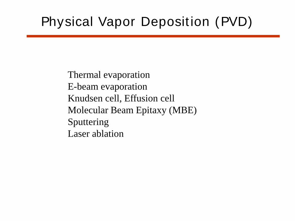
Physical Vapor Deposition (PVD)
Thermal evaporationE-beam evaporationKnudsen cell, Effusion cellMolecular Beam Epitaxy (MBE)SputteringLaser ablation
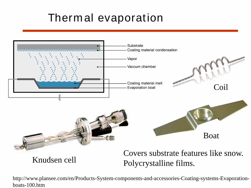
Boat
Thermal evaporation
http://www.plansee.com/en/Products-System-components-and-accessories-Coating-systems-Evaporation-boats-100.htm
Knudsen cellCovers substrate features like snow.Polycrystalline films.
Coil

Titanium Sublimation Pump (TSP)
This is a kind of getter pump
http://www.lesker.com/newweb/vacuum_pumps/ionpump_gamma_ionpump_tisub.cfm

http://www.plansee.com/en/Products-System-components-and-accessories-Coating-systems-Evaporation-boats-100.htm

http://www.polyteknik.com/E-Beam_Evaporation.htmlhttp://www.directindustry.com/prod/omicron/evaporators-electron-beam-20757-1062065.html
Electron-beam evaporation
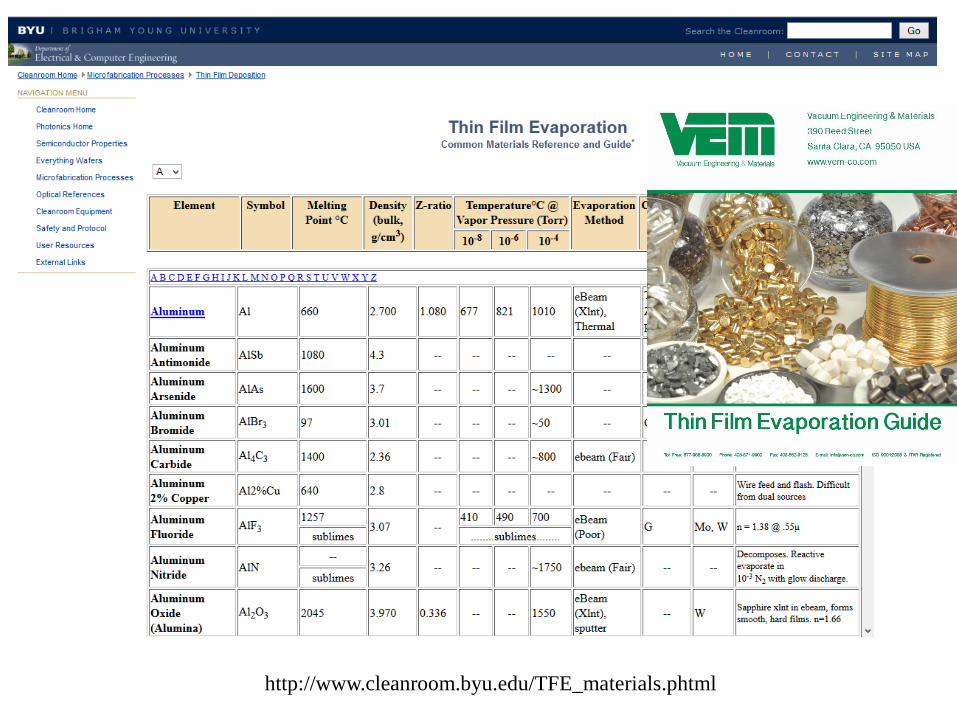
http://www.cleanroom.byu.edu/TFE_materials.phtml

http://www.eps.hw.ac.uk/institutes/photonics-quantum-sciences/mbe.htmhttp://www.fkf.mpg.de/273938/30_Oxide_MBE_Lab
Electron-beam evaporation
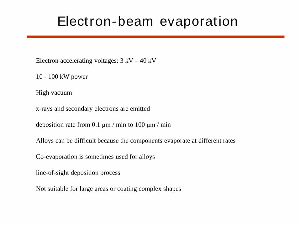
Electron accelerating voltages: 3 kV – 40 kV
10 - 100 kW power
High vacuum
x-rays and secondary electrons are emitted
deposition rate from 0.1 μm / min to 100 μm / min
Alloys can be difficult because the components evaporate at different rates
Co-evaporation is sometimes used for alloys
line-of-sight deposition process
Not suitable for large areas or coating complex shapes
Electron-beam evaporation
http
://w
ww.
iue.
tuw
ien.
ac.a
t/phd
/was
shub
er/n
ode5
1.ht
ml
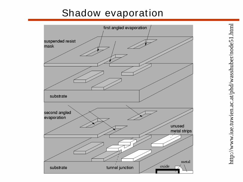
Shadow evaporation

2
mV
nA
0.50
1
Single electron transistor
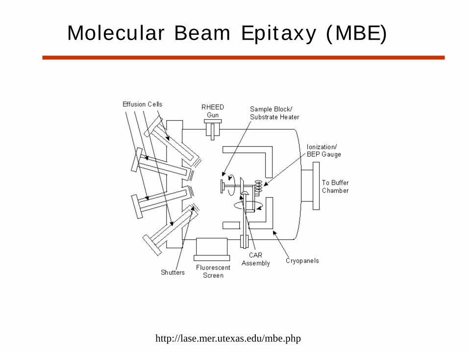
Molecular Beam Epitaxy (MBE)
http://lase.mer.utexas.edu/mbe.php
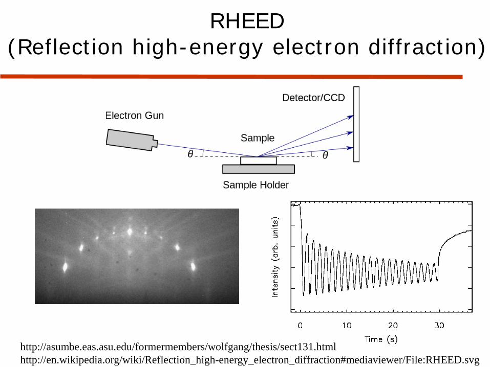
RHEED (Reflection high-energy electron diffraction)
http://asumbe.eas.asu.edu/formermembers/wolfgang/thesis/sect131.htmlhttp://en.wikipedia.org/wiki/Reflection_high-energy_electron_diffraction#mediaviewer/File:RHEED.svg
M. Ohring, The Material Science of Thin Films, Academic Press, 1992.
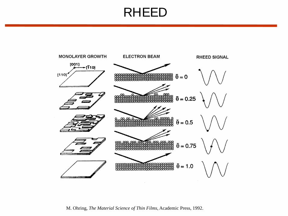
RHEED

Molecular dynamics
Calculate the motions of the atoms at the surface.

Growth modes
http://en.wikipedia.org/wiki/Stranski%E2%80%93Krastanov_growth
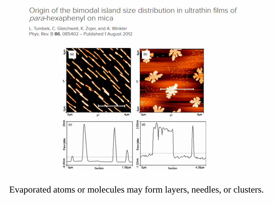
Evaporated atoms or molecules may form layers, needles, or clusters.

Heteroepitaxy
Fransila
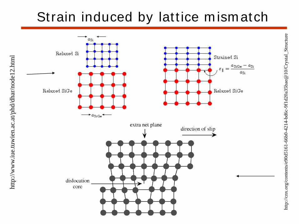
Strain induced by lattice mismatchht
tp://
ww
w.iu
e.tu
wie
n.ac
.at/p
hd/d
har/n
ode1
2.ht
ml
http
://cn
x.or
g/co
nten
ts/e
90d5
161-
66b0
-421
4-bd
6c-9
f1d2
0a35
bae@
10/C
ryst
al_S
truct
ure
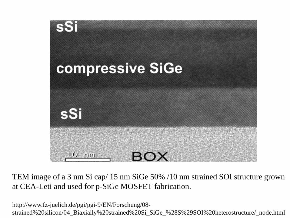
TEM image of a 3 nm Si cap/ 15 nm SiGe 50% /10 nm strained SOI structure grown at CEA-Leti and used for p-SiGe MOSFET fabrication.
http://www.fz-juelich.de/pgi/pgi-9/EN/Forschung/08-strained%20silicon/04_Biaxially%20strained%20Si_SiGe_%28S%29SOI%20heterostructure/_node.html
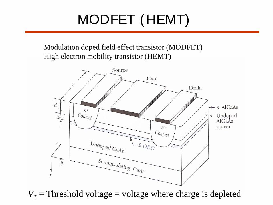
MODFET (HEMT)
Modulation doped field effect transistorHigh electron mobility transistor
VT = Threshold voltage = voltage where charge is depleted
Modulation doped field effect transistor (MODFET)High electron mobility transistor (HEMT)

Heterostructure
pn junction formed from two semiconductors with different band gaps
PhD Thesis Sergey Smirnovhttp://www.iue.tuwien.ac.at/phd/smirnov/node71.html
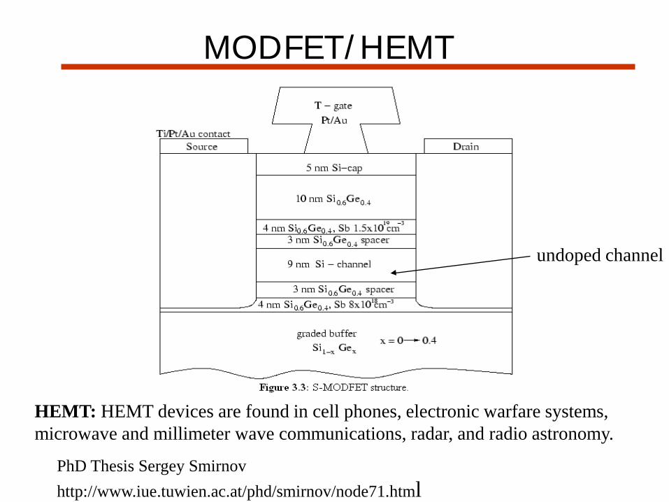
undoped channel
HEMT: HEMT devices are found in cell phones, electronic warfare systems, microwave and millimeter wave communications, radar, and radio astronomy.
MODFET/HEMT
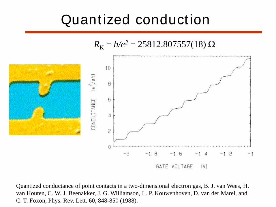
Quantized conduction
Quantized conductance of point contacts in a two-dimensional electron gas, B. J. van Wees, H. van Houten, C. W. J. Beenakker, J. G. Williamson, L. P. Kouwenhoven, D. van der Marel, and C. T. Foxon, Phys. Rev. Lett. 60, 848-850 (1988).
RK = h/e2 = 25812.807557(18) Ω
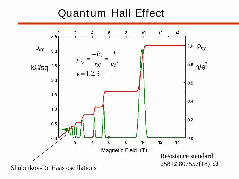
Quantum Hall Effect
Shubnikov-De Haas oscillations
Resistance standard25812.807557(18) Ω
2
1, 2,3
zxy
B hne ve
v
ρ −= =
=

Light emitting diodes
absorptionreflectiontotal internal reflection
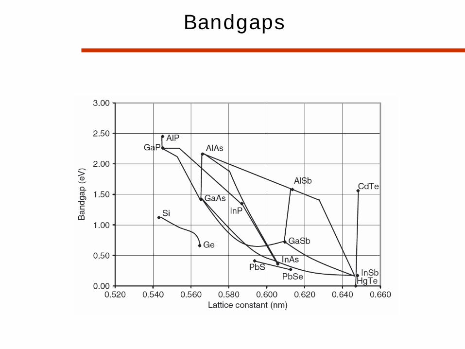
Bandgaps
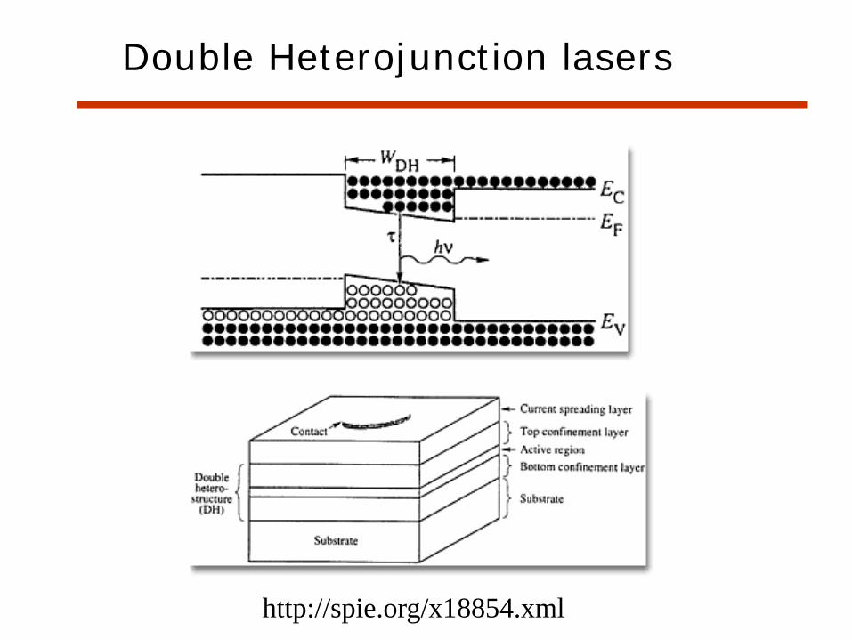
Double Heterojunction lasers
http://spie.org/x18854.xml