Molecular Junctions – Made to Measure (by Electro … Junctions – Made to . Measure (by...
25
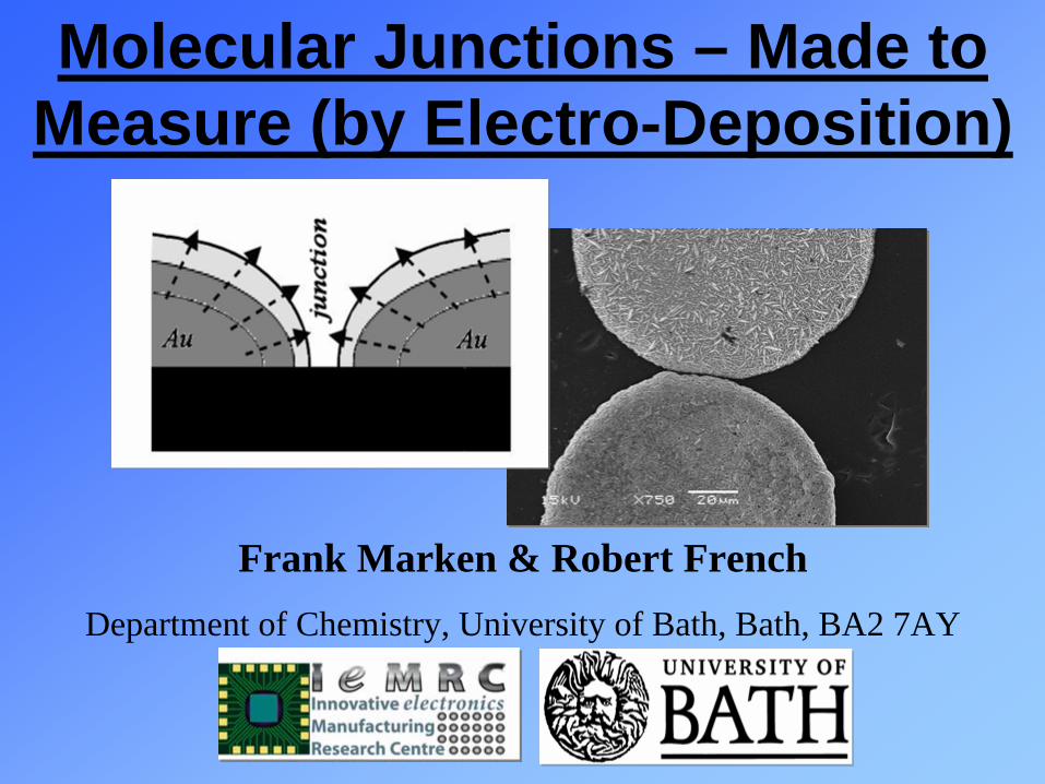
Molecular Junctions – Made to Measure (by Electro-Deposition) Frank Marken & Robert French Department of Chemistry, University of Bath, Bath, BA2 7AY
Transcript of Molecular Junctions – Made to Measure (by Electro … Junctions – Made to . Measure (by...
Molecular Junctions – Made to Measure (by Electro-Deposition)
Frank Marken & Robert French Department of Chemistry, University of Bath, Bath, BA2 7AY

Acknowledgments:IeMRC (Innovative electronic Manu- facturing Research Council)
Hugh Perrott (Department of Physics, Bath) and John Bates (IPTME, Loughborough) for Electron Microscopy (SEM) imaging
Sergey Gordeev (Department of Physics) for collaboration and discussion
Paul Raithby (Department of Chemistry) for help and discussion
Martin Goosey (IeMRC) for help and discussion
Content
1. Aims & Introduction
2. Assembly of sub-monolayer gold nanoparticle junction arrays
3. Electrochemical formation of junctions at double disc electrodes
4. Towards non-dendritic growth
5. Humidity and thiol sensitivity of double disc electrodes
6. Summary
7. Outlook

1. Aims
• Cost effective production of molecular gap junctions
• Implement a bipotentiostatic electrochemical methodology
• Junction formation by tunnel current control or using templating agents
• Application of molecular gap junctions as sensors

1. Introduction• Nano or molecular gap junctions are the key to future electronic devices getting ever smaller and more effective
• Fabrication methods based on high vacuum deposition and direct mani- pulation on the nanoscale could be problematic and alternatives are desirable.
• The electrochemical methodology is attractive and based on simple electro-deposition processes which can be controlled externally by applied potentials.
• We aim to develop a novel electrochemical protocol to produce molecular gap junctions and to study their applications.
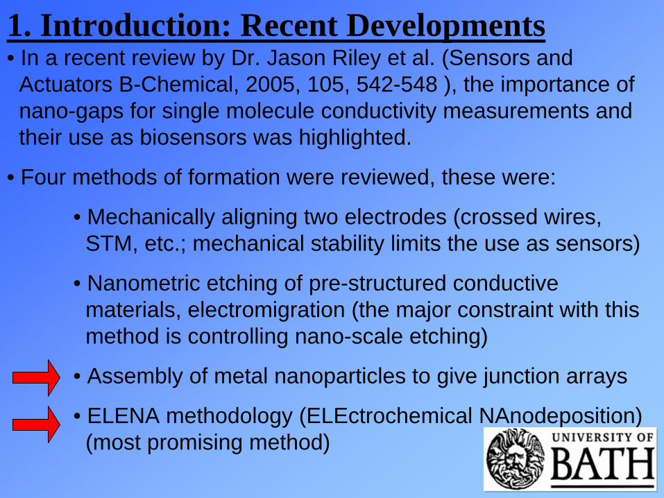
1. Introduction: Recent Developments• In a recent review by Dr. Jason Riley et al. (Sensors and Actuators B-Chemical, 2005, 105, 542-548 ), the importance of nano-gaps for single molecule conductivity measurements and their use as biosensors was highlighted.
• Four methods of formation were reviewed, these were:
• Mechanically aligning two electrodes (crossed wires, STM, etc.; mechanical stability limits the use as sensors)
• Nanometric etching of pre-structured conductive materials, electromigration (the major constraint with this method is controlling nano-scale etching)
• Assembly of metal nanoparticles to give junction arrays
• ELENA methodology (ELEctrochemical NAnodeposition) (most promising method)

2. Assembly of Sub-Monolayer Gold Nanoparticle Junction Arrays
Initial experiments carried out using junction arrays rather than electrochemically deposited molecular gapsFabrication method:
Basic UV lithography used to etch out ITO electrodes
Negatively charged gold nano-particles (20 nm diam.) from aqueous solution withPDDAC (poly- diallyldimethylammonium chloride) poly-cationic binder
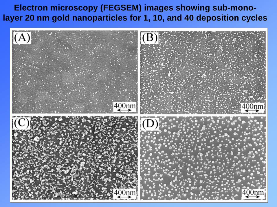
Electron microscopy (FEGSEM) images showing sub-mono- layer 20 nm gold nanoparticles for 1, 10, and 40 deposition cycles
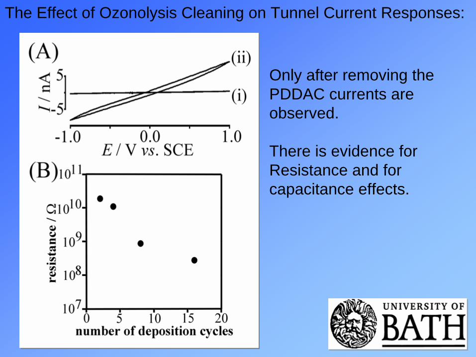
The Effect of Ozonolysis Cleaning on Tunnel Current Responses:
Only after removing the PDDAC currents are observed.
There is evidence for Resistance and for capacitance effects.

Sub-mono-layer gold nano- particle arrays sensitive to relative humidity:
Resistance and “apparent capacitance” information is obtained from voltammo- grams as a function of RH:
Molecular species like thiols can be reproducibly immobilised into and removed from junction arrays. Tunnel currents are measured in vacuum conditions:
Thiols have been immobilised and investigated and finally removed with UV-ozonolysis:

A model to explain humidity effects: a thin water film develops on ozone-cleaned probe surface; currents consist of (i) electronic tunnelling current and (ii) current from lateral ion conduction.
The apparent capacitance reflects the ITO/water surface double layer capacitance (or a part of it).
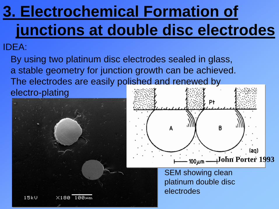
3. Electrochemical Formation of junctions at double disc electrodes
IDEA: By using two platinum disc electrodes sealed in glass, a stable geometry for junction growth can be achieved. The electrodes are easily polished and renewed by electro-plating
SEM showing clean platinum double disc electrodes
John Porter 1993

• Using dual electrode and a bipotentiostat to apply two different potentials to the individual platinum discs
• Junction growth occurs until “collision” and collapse of the deposition potential
• The initial step was to deposit gold at -1.5V on one platinum disc (Disc A, see SEM)
• CV showing simple reduction and oxidation of gold at disc surface (different plating baths were tested).
• SEM showing one platinum disc gold coated

• The second step was bipotentiostatic growth was run in one cell with two working electrodes
WE1: dominant electrode
WE2: deposition electrode
CE: counter electrode
RE: reference electrode
• Disc A was wired as working electrode one (WE1) and set to a deposition potential of -2.0 V vs. SCE
• Disc B was wired to working electrode two (WE2) and set at a constant potential of –1.5 V vs. SCE

Two situation’s occurred depending on the potential chosen for WE1:
• stable connection upon reaching the contact point (see potential region “contact”)
• onset of oscillation upon contact due to repeated dissolution – deposition cycling (region “oscillation”)
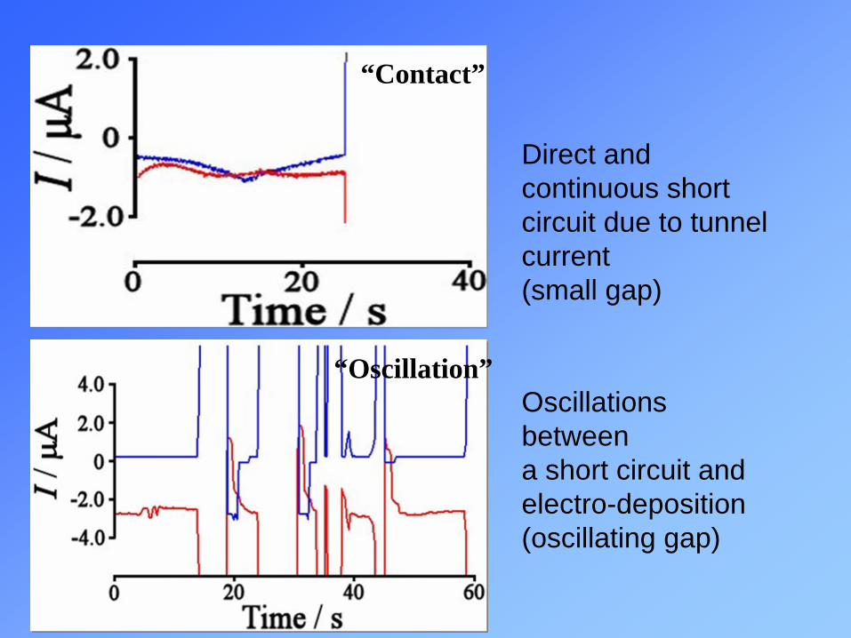
Direct and continuous short circuit due to tunnel current (small gap)
Oscillations between a short circuit and electro-deposition (oscillating gap)
“Contact”
“Oscillation”

SEM images of double-disc junctions. Initially, dendritic gold growth was leading to “buried” junctions:
4. Achieving non-dendritic growth:
The dendritic nature of the electrodes is detrimental to the study for three reasons
(i) The highly crystalline structures ‘bury’ junction preventing characterisation via SEM
(ii) The dendritic junctions are geometrically more complex and less reproducible
(iii) Dendritic growth is mechanically unstable preventing any liquid phase experiments
We hope that by growing smoother more drop like surfaces we can create more well-defined junctions with increased mechanical stability

To achieve smoother gold deposition ….(i) the applied plating potential was chosen more positive to slow
down deposition and nucleation(ii) addition of PDDAC was attempted to suppress dendrites
(A)
(B)
(C)Alkaline cyanide bath with agitation, 50 oC


5. Humidity and thiol sensitivity of double disc junctions
The change from ambient air to argon or to vacuum causes a dramatic change of behaviour of the double-disc junction:
In ambient air
Under vacuum
Resistance and “apparent capacitance” information is obtained from voltammograms.
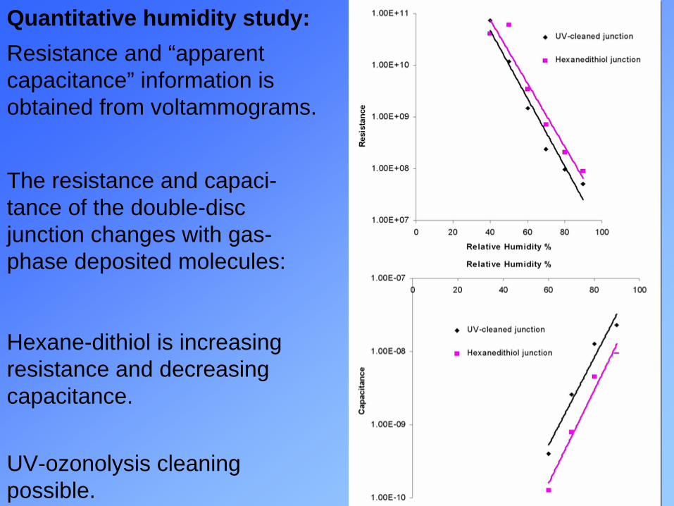
Quantitative humidity study:
The resistance and capaci- tance of the double-disc junction changes with gas- phase deposited molecules:
Hexane-dithiol is increasing resistance and decreasing capacitance.
UV-ozonolysis cleaning possible.
• New simple protocol for production of junctions has been developed.
• Original attempts dendritic but have proven principles. The have also proven useful in testing UV-ozonolysis cleaning employed to compare humidity and dithiol deposition effects in single junctions.
• Process has been refined to improve mechanical stability of junction allowing for a more thorough investigation.
6. Summary
7. Future work• Making better junctions
• Can junctions be grown with different gap sizes?
• Using templating agents to form molecular junctions
• Investigate if humidity work can be used to characterise the junctions formed
• Liquid phase experiments
• “Guided growth”

Acknowledgments:IeMRC (Innovative electronic Manu- facturing Research Council)
Hugh Perrott (Department of Physics, Bath) and John Bates (IPTME, Loughborough) for Electron Microscopy (SEM) imaging
Sergey Gordeev (Department of Physics) for collaboration and discussion
Paul Raithby (Department of Chemistry) for help and discussion
Martin Goosey (IeMRC) for help and discussion