PACSystems Memory Xchange Modules - Logic Control Memory... · The Memory Xchange modules use...
76
GE Intelligent Platforms GFK-2300E PACSystems* Memory Xchange Modules User's Manual
Transcript of PACSystems Memory Xchange Modules - Logic Control Memory... · The Memory Xchange modules use...
GEIntelligent Platforms
GFK-2300E
PACSystems*Memory Xchange ModulesUser's Manual

These instructions do not purport to cover all details or variations in equipment, nor to provide for every possiblecontingency to be met during installation, operation, and maintenance. The information is supplied for informationalpurposes only, and GE makes no warranty as to the accuracy of the information included herein. Changes, modifications,and/or improvements to equipment and specifications are made periodically and these changes may or may not be reflectedherein. It is understood that GE may make changes, modifications, or improvements to the equipment referenced herein or tothe document itself at any time. This document is intended for trained personnel familiar with the GE products referencedherein.
GE may have patents or pending patent applications covering subject matter in this document. The furnishing of thisdocument does not provide any license whatsoever to any of these patents.
GE provides the following document and the information included therein as is and without warranty of any kind, expressedor implied, including but not limited to any implied statutory warranty of merchantability or fitness for particular purpose.
For further assistance or technical information, contact the nearest GE Sales or Service Office, or an authorized GE SalesRepresentative.
Revised: May 2014Issued: Jun 2005
Copyright © 2005 - 2014 General Electric Company, All rights reserved.___________________________________* Indicates a trademark of General Electric Company and/or its subsidiaries.All other trademarks are the property of their respective owners.
Refer to the section, Contact Information for support on this product.
Please send documentation comments or suggestions to [email protected]

Document UpdatesLocation Description
Chapter 2, QuickStart In step 3, added clarification on cable type requirements.
Chapter 3, Installation andConfiguration
The section, RMX128/RMX228 LEDs added RMX228.The section, Installing the Memory Xchange Module in an RX3i Rack, added clarificationfor hot swapped RMX modules.The section, Network Connection, updated information and added RMX228.The section Fiber-optic Cables, updated information and added RMX228 specifications.
GFK-2300E User's Manual 3

Safety Symbol Legend
Warning
Indicates a procedure, condition, or statement that, if notstrictly observed, could result in personal injury or death.
Caution
Indicates a procedure, condition, or statement that, if notstrictly observed, could result in damage to or destruction ofequipment.
Attention
Indicates a procedure, condition, or statement that should bestrictly followed to improve these applications.
Contact InformationIf you purchased this product through an Authorized Channel Partner, please contact the seller directly.
General Contact Information
Online technical support and GlobalCare http://support.ge-ip.com
Additional information http://www.ge-ip.com/
Solution Provider [email protected]
Technical Support
If you have technical problems that cannot be resolved with the information in this manual, please contact us bytelephone or email, or on the web at http://support.ge-ip.com
Americas
Online Technical Support http://support.ge-ip.com
Phone 1-800-433-2682
International Americas Direct Dial 1-780-420-2010 (if toll free 800 option is unavailable)
Technical Support Email [email protected]
Customer Care Email [email protected]
Primary language of support English
Europe, the Middle East, and Africa
Online Technical Support http://support.ge-ip.com
Phone + 800-1-433-2682
EMEA Direct Dial+ 420-23-901-5850 (if toll free 800 option is unavailable or dialing froma mobile telephone)
Technical Support Email [email protected]
Customer Care Email [email protected]
Primary languages of support English, French, German, Italian, Czech, Spanish
Asia Pacific
Online Technical Support http://support.ge-ip.com
Phone+ 86-400-820-8208+ 86-21-3217-4826 (India, Indonesia, and Pakistan)
Technical Support Email
[email protected] (China)
[email protected] (Japan)
[email protected] (remaining Asia customers)
Customer Care [email protected]
[email protected] (China)
GFK-2300E User's Manual 5

Notes
6 GFK-2300E PACSystems Memory Xchange Modules

Contents1 Introduction ....................................................................................................................................... 91.1 Related Documentation........................................................................................................................... 10
1.2 Overview ............................................................................................................................................. 10
1.2.1 Basic Memory Xchange Operation ..................................................................................................... 11
1.2.2 Sample Memory Xchange Network .................................................................................................... 11
1.3 Memory Xchange Features ...................................................................................................................... 12
1.3.1 RX3i Reflective Memory Module Features .......................................................................................... 12
1.3.2 IC695CMX128, IC695RMX128, and IC695RMX228 Functional Compatibility ......................................... 13
1.3.3 RX7i Reflective Memory Module Features .......................................................................................... 14
1.3.4 IC698CMX016 and IC698RMX016 Functional Compatibility ................................................................. 15
1.3.5 Reflective Memory Hub .................................................................................................................. 15
2 QuickStart......................................................................................................................................... 173 Installation and Configuration .................................................................................................... 213.1 RX3i Memory Xchange Module User Features............................................................................................ 21
3.1.1 CMX128 LEDs .............................................................................................................................. 21
3.1.2 RMX128/RMX228 LEDs ................................................................................................................. 22
3.1.3 Optical Transceiver ......................................................................................................................... 22
3.2 RX7i Memory Xchange Module User Features............................................................................................ 23
3.2.1 Role Switch (RMX Only) ................................................................................................................ 24
3.2.2 Node ID ........................................................................................................................................ 24
3.2.3 Redundant Transfer Mode Operation .................................................................................................. 24
3.2.4 Network Memory Offset................................................................................................................... 25
3.2.5 Rogue Packet Detection and Removal ................................................................................................. 26
3.3 Physical Installation ............................................................................................................................... 27
3.3.1 RX3i Memory Xchange Modules ....................................................................................................... 27
3.3.2 RX7i Memory Xchange Modules ....................................................................................................... 28
3.4 Network Connection .............................................................................................................................. 29
3.4.1 VMICBL-000-F5-0xx Cable Lengths.................................................................................................. 29
3.4.2 Fiber-optic Connectors ..................................................................................................................... 30
3.4.3 Fiber-optic Cables ........................................................................................................................... 30
3.5 Hardware Configuration.......................................................................................................................... 31
3.5.1 Configuring a Memory Xchange Module............................................................................................. 31
3.5.2 Configuration Parameters ................................................................................................................. 31
4 Basic Operation .............................................................................................................................. 354.1 Powerup and Initialization ....................................................................................................................... 35
4.2 BUS_ Functions .................................................................................................................................... 36
4.2.1 Data Integrity of RMWand TS Bus Accesses ....................................................................................... 37
4.3 Multiple Writes to Network Memory ......................................................................................................... 38
4.4 Data Transfer Time ................................................................................................................................ 39
GFK-2300E User's Manual 7
4.4.1 RX3i Read/Write Transfer Times ....................................................................................................... 39
4.4.2 RX7i Read/Write Transfer Times ....................................................................................................... 39
4.4.3 Estimating Total Transfer Time.......................................................................................................... 40
4.5 Special Considerations for Stores of Configuration....................................................................................... 41
5 Advanced Operation...................................................................................................................... 435.1 Module Interrupts .................................................................................................................................. 44
5.1.1 Interrupt Initialization Logic ............................................................................................................. 45
5.1.2 Interrupt Handling Logic .................................................................................................................. 46
5.1.3 Associating Module Interrupts with Logic............................................................................................ 47
5.1.4 Dynamic Masking of Module Interrupts .............................................................................................. 48
5.2 Network Interrupts ................................................................................................................................. 49
5.2.1 Sending Network Interrupts .............................................................................................................. 49
5.2.2 Receiving Network Interrupts ............................................................................................................ 49
5.3 Memory Parity Checking ........................................................................................................................ 51
5.3.1 Logic for Detecting and Clearing a Parity Error .................................................................................... 52
5.4 On-demand Memory Clear ...................................................................................................................... 53
5.5 Checking Ring Integrity .......................................................................................................................... 53
5.6 Optimizing Network Bandwidth ............................................................................................................... 54
5.6.1 Using Network Interrupts to Balance Network Load .............................................................................. 55
Appendix A-Memory Xchange Module Specifications ............................................................... 57Appendix B-Register Definitions...................................................................................................... 59
Region 2: Primary Control and Status Registers........................................................................................... 60
Local Control and Status Register (LCSR) ........................................................................................... 61
Local Interrupt Status Register (LISR) ................................................................................................ 63
Local Interrupts Enable Register (LIER).............................................................................................. 65
Registers for Generating Network Interrupts......................................................................................... 65
Registers for Receiving Network Interrupts .......................................................................................... 66
Region3: Auxiliary Control and Status Registers.......................................................................................... 69
Offset 440h.................................................................................................................................... 69
Offset 441h.................................................................................................................................... 69
Offset 442h.................................................................................................................................... 70
Offset 445h.................................................................................................................................... 70
Offset 446h.................................................................................................................................... 71
Region 4: Interrupt Acknowledge Register ................................................................................................. 71
Interrupt Acknowledge Register (IAKR) ............................................................................................. 71
Appendix C-Reflective Memory Module Status Bits.................................................................... 72IC695CMX128, IC695RMX128, and IC695RMX228................................................................................... 72
Instructions for Usage ...................................................................................................................... 72
8 GFK-2300E PACSystems Memory Xchange Modules

1 IntroductionThis manual describes the features, installation, and operation of the following MemoryXchange modules in a PACSystems reflective memory network:
IC695RMX228 RX3i Redundancy Memory Xchange (RMX) Single-mode module
IC695CMX128 RX3i Control Memory Xchange (CMX) module
IC695RMX128 RX3i Redundancy Memory Xchange (RMX) module
IC698CMX016 RX7i Control Memory Xchange (CMX) module
IC698RMX016 RX7i Redundancy Memory Xchange (RMX) module
This chapter presents an overview ofMemory Xchange Operation, and a summary ofMemory Xchange Features and functional compatibility.
For additional information, refer to the following chapters:
• Chapter 2, QuickStart – Provides an overview of the steps needed to configure andoperate a reflective memory network and to verify Memory Xchange operation.
• Chapter 3, Installation and Configuration – describes user features, and providesprocedures for physical installation and software configuration.
• Chapter 4, Basic Operation – describes the operation of basic Memory Xchangemodule functions and how to access them.
• Chapter 5, Advanced Operation – describes how to use the advanced capabilities ofthe Memory Xchange module
• Appendix A, Memory Xchange Module Specifications – provides performance andenvironmental specifications.
• Appendix B, Register Definitions – provides detailed definitions of the module’sregisters.
Introduction GFK-2300E User's Manual 9
1.1 Related DocumentationGFK-2222, PACSystems CPU Reference ManualGFK-2223, PACSystems RX7i Installation ManualGFK-2314 , PACSystems RX3i System ManualGFK-2235, PACSystems RX7i User's Guide to Integration of VME ModulesGFK 2308, PACSystems Hot Standby CPU Redundancy User’s ManualGFK-1918, Proficy Machine Edition Logic Developer Getting Started
For the most recent versions of PACSystems and related documentation, visit the GEIntelligent Platforms website: http://www.ge-ip.com/
1.2 OverviewThe Memory Xchange modules use reflective memory technology, which allows thedeterministic sharing of data among Controllers and other computing devices on ahigh-speed fiber optic network. Deterministic networks enable sharing of data within apredetermined time interval. The network can be made up of any combination of thesemodules and other reflective memory devices that are network compatible with the GEIntelligent Platforms 5565 family. Each such device is a node on the network. A reflectivememory network can contain up to 256 nodes. Whenever data is written to one node, allnodes on the network are automatically updated with the new data.
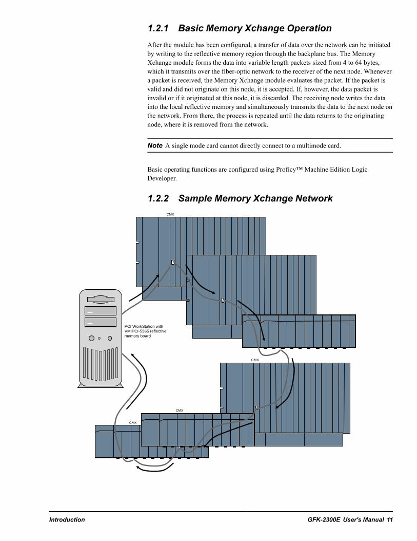
Each node in the reflective memory network is connected in a daisy-chained loop usingfiber-optic cables. The transmitter of the first node is tied to the receiver of the second.The transmitter of the second node is tied to the receiver of the third node, and so on, untilthe loop is completed back at the receiver of the first node. The figure in the section,Sample Memory Xchange Network shows an example of a seven-node reflective memorynetwork.
Note A hub is required to connect a single mode fiber device into a ring with multi modefiber devices. Hubs are not allowed when connecting redundant pairs.
The RMX modules can be used in a redundant system (two CPUs), as part of aredundancy link. A complete redundancy link consists of one RMX in the primary unit,one RMX in the secondary unit, and high-speed fiber optic cables connecting them toeach other. This must be a two-node ring: no other reflective memory nodes are allowedto be part of this fiber optic network. When the RMX is being used as redundancy link, itcannot be used as a general-purpose Memory Xchange module. When the RMX is notbeing used as a redundancy link, it is functionally identical to the CMX module.
For details on the operation of a PACSystems Hot Standby CPU redundancy system, referto the PACSystems Hot Standby CPU Redundancy User’s Manual, GFK 2308.
10 GFK-2300E PACSystems Memory Xchange Modules
1.2.1 Basic Memory Xchange OperationAfter the module has been configured, a transfer of data over the network can be initiatedby writing to the reflective memory region through the backplane bus. The MemoryXchange module forms the data into variable length packets sized from 4 to 64 bytes,which it transmits over the fiber-optic network to the receiver of the next node. Whenevera packet is received, the Memory Xchange module evaluates the packet. If the packet isvalid and did not originate on this node, it is accepted. If, however, the data packet isinvalid or if it originated at this node, it is discarded. The receiving node writes the datainto the local reflective memory and simultaneously transmits the data to the next node onthe network. From there, the process is repeated until the data returns to the originatingnode, where it is removed from the network.
Note A single mode card cannot directly connect to a multimode card.
Basic operating functions are configured using Proficy™ Machine Edition LogicDeveloper.
1.2.2 Sample Memory Xchange Network
CMX
PCI WorkStation with VMIPCI-5565 reflective memory board
CMX
CMX
CMX
Introduction GFK-2300E User's Manual 11

1.3 Memory Xchange Features
1.3.1 RX3i Reflective Memory Module FeaturesA PACSystems RX3i main rack supports a maximum of six Memory Xchange modules.
• PACSystems RX3i single slot form factor.
• 128 Mbytes reflective memory with parity.
• Software configuration of all nodeparameters (no jumper or switch settingsrequired).
• No RX3i CPU processing required to operatethe network.
• Network-compatible with the GE IntelligentPlatforms 5565 family of reflective memorydevices.
• Connection with multimode fiber up to 1000 ft(304.80 m) or
• Connection with single mode fiber supportsup to 32,808 ft 4 in (10 Kms)
• Dynamic packet sizes of 4 to 64 bytes,controlled by the CMX module.
• Network transfer rate of 43 Mbyte/s (4 bytepackets) to 174 Mbyte/s (64 byte packets)
• Network link speed of 2.1 Gbits/s
• Programmable module interrupt.
• Four general-purpose network interrupts with32 bits of data each.
• Network error detection.
• Up to 256 nodes per network.
• Redundant transfer mode operation. Thisoptional mode reduces the chance of a datapacket being dropped from the network.
• Configurable network memory offset forcompatibility with RX7i Memory Xchangeapplications.
CMX128
OK
CONFIG
SIG DETECT
OWN DATA
NODE
TX (FRONT)
RX (BACK)
RMX128
OK
LINK OK
SIG DETECT
OWN DATA
ROLESWITCH
0
1
READY
ACTIVE
READY
ACTIVE
NODE
RX (BACK)
TX (FRONT)
MULTI MODE FIBER
LOCAL
REMOTE
RMX228
OK
LINK OK
SIG DETECT
OWN DATA
ROLESWITCH
0
1
READY
ACTIVE
READY
ACTIVE
NODE
RX (BACK)
TX (FRONT)
SINGLE MODE FIBER
LOCAL
REMOTE
12 GFK-2300E PACSystems Memory Xchange Modules
1.3.2 IC695CMX128, IC695RMX128, andIC695RMX228 Functional Compatibility
Note The CMX128, RMX128, CMX016, RMX016 (multi mode interface) cannot bedirectly connected to the RMX228 (single mode interface).
• PACSystems RX3i CPU with firmware version 5.50 or later for CMX128 andPACSystems RX3i CPU with firmware version 5.70 or later for RMX128 andPACSystems RX3i CPU with firmware version 8.15 or later for RMX228.
• Programming software: Proficy Machine Edition Logic Developer, version 5.8 orlater for CMX128 and Proficy Machine Edition Logic Developer, version 5.9 SIM1or later for RMX128 and Proficy Machine Edition Logic Developer, version 8.5SIM2 or later for RMX228.
• Only the RMX can operate as a redundancy link. Redundancy link operation requiresa CPU that supports CPU redundancy, such as the IC695CRU320.
• Compatible with reflective memory devices in the GE Intelligent Platforms 5565family. The PACSystems Memory Xchange module does not operate with otherreflective memory families offered by GE Intelligent Platforms.
Introduction GFK-2300E User's Manual 13

1.3.3 RX7i Reflective Memory Module Features
An RX7i main rack supports a maximum of four Memory Xchangemodules in any combination of RMX and CMX modules. When usingCPU redundancy, up to two RMX modules in a rack can be configured asredundancy links.• PACSystems single slot form factor.
• 16 Mbytes reflective memory with parity.
• Software configuration of all node parameters (no jumper or switchsettings required).
• No PACS CPU processing required to operate the network.
• Network-compatible with the GE Intelligent Platforms 5565 family ofreflective memory devices.
• Connection with multimode fiber up to 1000 ft. (304.80 m).
• Dynamic packet sizes of 4 to 64 bytes, controlled by the MemoryXchange module.
• Network transfer rate of 43 Mbyte/s (4 byte packets) to 174 Mbyte/s(64 byte packets)
• Network link speed of 2.1 Gbits/s
• Programmable VMEbus interrupt output.
• Four general-purpose network interrupts with 32 bits of data each.
• Network error detection.
• Up to 256 nodes per network.
• Redundant transfer mode operation. This optional mode reduces thechance of a data packet being dropped from the network.
• Configurable network memory offset allows you to assign nodes on anetwork to groups according to the 16 MB segment in the networkaddress space that they use.
IC698CMX016
OK CONFIG
OWN DATA
SIGNAL DETECT
TX
RX
CMX016
IC698RMX016
OK LINK OK
LOCAL ACTIVE
REMOTE
ACTIVE
OWN DATA
SIGNAL DETECT
TX
RX
ROLE SWITCH
1
0
RMX016
READY
READY
14 GFK-2300E PACSystems Memory Xchange Modules
1.3.4 IC698CMX016 and IC698RMX016 FunctionalCompatibility• PACSystems RX7i CPU with firmware version 2.0 or later.
• Only an RMX can operate as a redundancy link. To operation as a redundancy link,RMX modules require a CPU that supports CPU redundancy, such as theIC698CRE020.
• Programming software: Proficy Machine Edition Logic Developer, version 4.5 orlater
• When used as a general-purpose reflective memory module, the RX7i MemoryXchange modules are compatible with reflective memory devices in the GEIntelligent Platforms 5565 family. The PACSystems Memory Xchange module doesnot operate with other reflective memory families offered by GE IntelligentPlatforms.
1.3.5 Reflective Memory HubThe VMIACC-5595 is a managed hub designed to operate with the GE IntelligentPlatforms 5565 family of Reflective Memory real-time network products. The ReflectiveMemory hub can automatically bypass ports when it detects a loss of signal or the loss ofvalid synchronization patterns, allowing the other nodes in the network to remainoperational.
For additional information, refer to the VMIACC-5595 2 Gb/s Reflective Memory HubInstallation Guide, 522-805595-000, which is available at http://www.ge-ip.com.
Introduction GFK-2300E User's Manual 15

Notes
16 GFK-2300E PACSystems Memory Xchange Modules
2 QuickStartThis chapter provides an overview of the steps needed to configure and operate a basicreflective memory network and to verify Memory Xchange operation.
Note For operation of an RMX in a redundancy system, refer to GFK 2308, PACSystemsHot Standby CPU Redundancy User’s Manual.
Performance Recommendations
• To transfer data most efficiently, use the minimum number of reads/writes possible.For example, use one long read/write instead of several. Length is specified in datasize (DWORDS).
• For maximum performance, Offset, which is specified in BYTES, should bespecified in numbers divisible by 4, so that bus accesses are DWORD aligned.
1. Install the Memory Xchange module in the rack system. If necessary, apply power tothe controller.
When power is applied to the module an internal loopback test occurs; the OWN DATAand SIGNAL DETECT indicators turn on briefly during this test. When the MemoryXchange module and the CPU are powered up and functioning properly, the module’s OKindicator is on.
Warning
RX7i modules do not support hot installation andremoval. Do not insert or remove RX7i modules withpower applied. This could cause the CPU to stop,damage the module, or result in personal injury.
Note RX3i Memory Xchange modules support hot insertion and removal.
For installation details, refer to chapter 3, the section, Physical Installation.
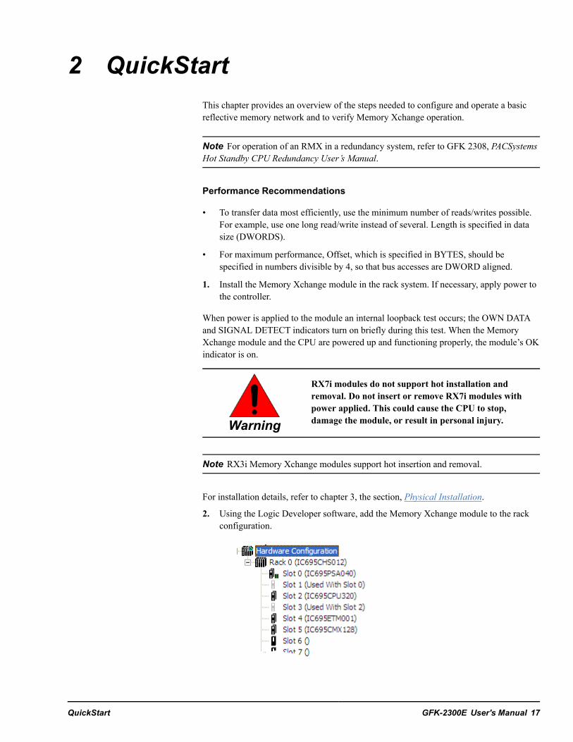
2. Using the Logic Developer software, add the Memory Xchange module to the rackconfiguration.
QuickStart GFK-2300E User's Manual 17
3. Connect the module to the network.
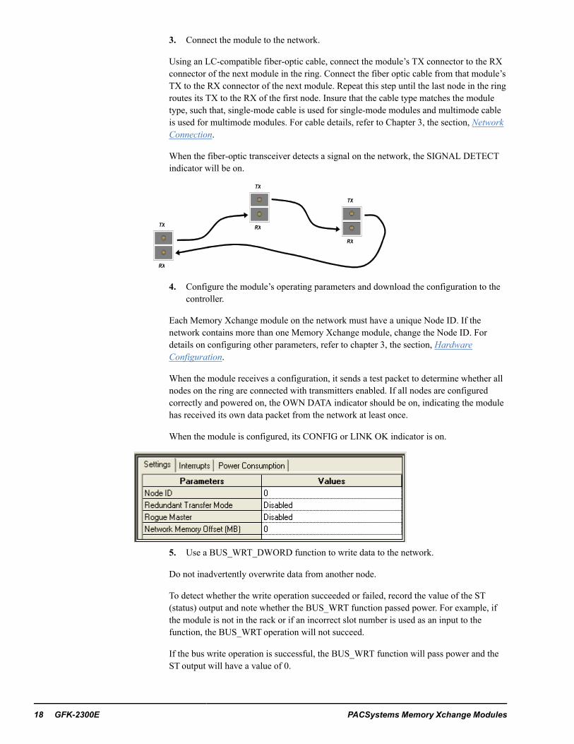
Using an LC-compatible fiber-optic cable, connect the module’s TX connector to the RXconnector of the next module in the ring. Connect the fiber optic cable from that module’sTX to the RX connector of the next module. Repeat this step until the last node in the ringroutes its TX to the RX of the first node. Insure that the cable type matches the moduletype, such that, single-mode cable is used for single-mode modules and multimode cableis used for multimode modules. For cable details, refer to Chapter 3, the section, NetworkConnection.
When the fiber-optic transceiver detects a signal on the network, the SIGNAL DETECTindicator will be on.
TX
RX
TX
RXTX
RX
4. Configure the module’s operating parameters and download the configuration to thecontroller.
Each Memory Xchange module on the network must have a unique Node ID. If thenetwork contains more than one Memory Xchange module, change the Node ID. Fordetails on configuring other parameters, refer to chapter 3, the section, HardwareConfiguration.
When the module receives a configuration, it sends a test packet to determine whether allnodes on the ring are connected with transmitters enabled. If all nodes are configuredcorrectly and powered on, the OWN DATA indicator should be on, indicating the modulehas received its own data packet from the network at least once.
When the module is configured, its CONFIG or LINK OK indicator is on.
5. Use a BUS_WRT_DWORD function to write data to the network.
Do not inadvertently overwrite data from another node.
To detect whether the write operation succeeded or failed, record the value of the ST(status) output and note whether the BUS_WRT function passed power. For example, ifthe module is not in the rack or if an incorrect slot number is used as an input to thefunction, the BUS_WRT operation will not succeed.
If the bus write operation is successful, the BUS_WRT function will pass power and theST output will have a value of 0.
18 GFK-2300E PACSystems Memory Xchange Modules
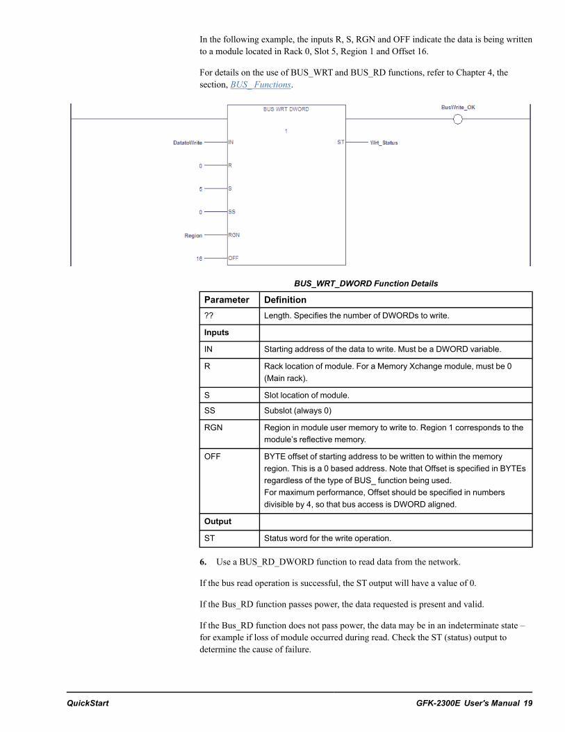
In the following example, the inputs R, S, RGN and OFF indicate the data is being writtento a module located in Rack 0, Slot 5, Region 1 and Offset 16.
For details on the use of BUS_WRT and BUS_RD functions, refer to Chapter 4, thesection, BUS_ Functions.
BUS_WRT_DWORD Function Details
Parameter Definition?? Length. Specifies the number of DWORDs to write.
Inputs
IN Starting address of the data to write. Must be a DWORD variable.
R Rack location of module. For a Memory Xchange module, must be 0(Main rack).
S Slot location of module.
SS Subslot (always 0)
RGN Region in module user memory to write to. Region 1 corresponds to themodule’s reflective memory.
OFF BYTE offset of starting address to be written to within the memoryregion. This is a 0 based address. Note that Offset is specified in BYTEsregardless of the type of BUS_ function being used.For maximum performance, Offset should be specified in numbersdivisible by 4, so that bus access is DWORD aligned.
Output
ST Status word for the write operation.
6. Use a BUS_RD_DWORD function to read data from the network.
If the bus read operation is successful, the ST output will have a value of 0.
If the Bus_RD function passes power, the data requested is present and valid.
If the Bus_RD function does not pass power, the data may be in an indeterminate state –for example if loss of module occurred during read. Check the ST (status) output todetermine the cause of failure.
QuickStart GFK-2300E User's Manual 19
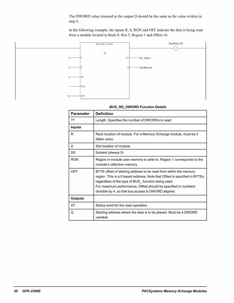
The DWORD value returned in the output Q should be the same as the value written instep 4.
In the following example, the inputs R, S, RGN and OFF indicate the data is being readfrom a module located in Rack 0, Slot 5, Region 1 and Offset 16.
BUS_RD_DWORD Function Details
Parameter Definition?? Length. Specifies the number of DWORDs to read.
Inputs
R Rack location of module. For a Memory Xchange module, must be 0(Main rack).
S Slot location of module.
SS Subslot (always 0)
RGN Region in module user memory to write to. Region 1 corresponds to themodule’s reflective memory.
OFF BYTE offset of starting address to be read from within the memoryregion. This is a 0 based address. Note that Offset is specified in BYTEsregardless of the type of BUS_ function being used.For maximum performance, Offset should be specified in numbersdivisible by 4, so that bus access is DWORD aligned.
Outputs
ST Status word for the read operation.
Q Starting address where the data is to be placed. Must be a DWORDvariable.
20 GFK-2300E PACSystems Memory Xchange Modules

3 Installation and ConfigurationThis chapter provides a guide to the user features, physical installation, and initialconfiguration of the Memory Xchange module.
Before you can use the Memory Xchange module, you must configure it using ProficyMachine Edition Logic Developer software. The programming software allows you tospecify a basic hardware configuration for the Memory Xchange module that allows it tooperate in a reflective memory network or as a redundancy link (RMX modules only).
3.1 RX3i Memory Xchange Module User Features
3.1.1 CMX128 LEDsLED Label Description
OK ON indicates the module andthe CPU are functioningproperly.
CMX128
OK
CONFIG
SIG DETECT
OWN DATA
NODE
TX (FRONT)
RX (BACK)
Optical Transceiver
(bottom view) TX
RX
CONFIG† ON indicates the module isconfigured.
SIG DETECT ON indicates the receiver isdetecting a fiber optic signal.
OWN DATA ON indicates the module hasreceived its own data packetfrom the network at least once.
† A reflective memory hub can be used to bypassa node that is not configured.
Installation and Configuration GFK-2300E User's Manual 21

3.1.2 RMX128/RMX228 LEDsLED Label Description
OK ON indicates the module isfunctioning properly.
OpticalTransceiver
(bottom view)
RMX128
OK
LINK OK
SIG DETECT
OWN DATA
ROLESWITCH
0
1
< LOCAL RDY
< LOCAL ACT
< REMOTE RDY
< REMOTE ACT
NODE
TX (BACK)
TX (FRONT)
MULTI MODE FIBER
RMX128
OK
LINK OK
SIG DETECT
OWN DATA
ROLESWITCH
0
1
READY
ACTIVE
READY
ACTIVE
NODE
RX (BACK)
TX (FRONT)
MULTI MODE FIBER
LOCAL
REMOTE
OpticalTransceiver
(bottom view)
RMX228
OK
LINK OK
SIG DETECT
OWN DATA
ROLESWITCH
0
1
< LOCAL RDY
< LOCAL ACT
< REMOTE RDY
< REMOTE ACT
NODE
TX (BACK)
TX (FRONT)
SINGLE MODE FIBER
RMX228
OK
LINK OK
SIG DETECT
OWN DATA
ROLESWITCH
0
1
READY
ACTIVE
READY
ACTIVE
NODE
RX (BACK)
TX (FRONT)
SINGLE MODE FIBER
LOCAL
REMOTE
LINK OK When used as a redundancylink, ON indicates the link isfunctioning properly. Whennot used as a redundancylink, ON indicates themodule is configured.
SIGDETECT
ON indicates the receiver isdetecting a fiber optic signal.
OWN DATA ON indicates the module hasreceived its own data packetfrom the network at leastonce.
LOCALREADY
ON indicates the local unit isready.
LOCALACTIVE
ON indicates the local unit isactive.
REMOTEREADY
ON indicates the remote unitis ready.
REMOTEACTIVE
ON indicates the remote unitis active.
3.1.3 Optical TransceiverThe optical transceiver, which is located on the bottom of the module, has two LC typefiber optic ports. The port labeled TX is the transmitter and the port labeled RX is thereceiver.
CMX modules are networked together using either simplex (single-fiber) or duplex(dual-fiber) fiber-optic cables. The specific cable construction depends on your operatingenvironment. For details on cables, refer to Chapter 3, the sections, Fiber-optic Cablesand Fiber-optic Connectors.
22 GFK-2300E PACSystems Memory Xchange Modules
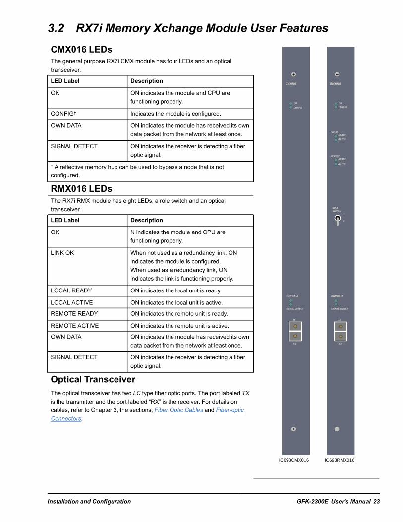
3.2 RX7i Memory Xchange Module User FeaturesCMX016 LEDs
IC698CMX016
OK CONFIG
OWN DATA
SIGNAL DETECT
TX
RX
CMX016
IC698RMX016
OK LINK OK
LOCAL ACTIVE
REMOTE
ACTIVE
OWN DATA
SIGNAL DETECT
TX
RX
ROLE SWITCH
1
0
RMX016
READY
READY
The general purpose RX7i CMX module has four LEDs and an opticaltransceiver.
LED Label Description
OK ON indicates the module and CPU arefunctioning properly.
CONFIG† Indicates the module is configured.
OWN DATA ON indicates the module has received its owndata packet from the network at least once.
SIGNAL DETECT ON indicates the receiver is detecting a fiberoptic signal.
† A reflective memory hub can be used to bypass a node that is notconfigured.
RMX016 LEDsThe RX7i RMX module has eight LEDs, a role switch and an opticaltransceiver.
LED Label Description
OK N indicates the module and CPU arefunctioning properly.
LINK OK When not used as a redundancy link, ONindicates the module is configured.When used as a redundancy link, ONindicates the link is functioning properly.
LOCAL READY ON indicates the local unit is ready.
LOCAL ACTIVE ON indicates the local unit is active.
REMOTE READY ON indicates the remote unit is ready.
REMOTE ACTIVE ON indicates the remote unit is active.
OWN DATA ON indicates the module has received its owndata packet from the network at least once.
SIGNAL DETECT ON indicates the receiver is detecting a fiberoptic signal.
Optical TransceiverThe optical transceiver has two LC type fiber optic ports. The port labeled TXis the transmitter and the port labeled “RX” is the receiver. For details oncables, refer to Chapter 3, the sections, Fiber Optic Cables and Fiber-opticConnectors.
Installation and Configuration GFK-2300E User's Manual 23
3.2.1 Role Switch (RMX Only)The Role switch is a spring-loaded two-position switch that rests in the OFF state. Whenthe RMX module is being used as a redundancy link, this switch allows you to manuallyswitch control from the active controller to the backup controller. To initiate the switchingof roles, lift the switch to the ON position for at least 1 second. The role switch state isde-bounced and filtered to prevent accidental activation.
When the RMX module is used as a node in a general-purpose reflective memorynetwork (i.e. not used as a redundancy link), the Role switch has no effect on moduleoperation.
3.2.2 Node IDEach node in a reflective memory network must have a unique Node ID, which mayrange from 0 through 255. Node ID is configured by the programming software.
3.2.3 Redundant Transfer Mode OperationRedundant Transfer mode is enabled or disabled using hardware configuration in theprogramming software. While in the Redundant Transfer mode, each packet is transferredon the network twice. The receiving node evaluates each redundant transfer. If no errorsare detected in the first transfer, it is used to update the on-board memory and the secondtransfer is discarded. If the first transfer contains an error, the second transfer is used toupdate the on-board memory provided it has no transmission error. If errors are detectedin both transfers, neither transfer is used and the data is completely removed from thenetwork. The Bad Data bit (Bit 01 of the LCSR in Region 2) is set if an error is detectedin either transfer.
Redundant Transfer mode greatly reduces the chance that data is dropped from thenetwork. However, the redundant transfer mode reduces the effective network transferrates by approximately 50 percent.
Note The Redundant Transfer mode pertains only to the method of transferring packetsover the network. It does not relate to redundancy link operation nor does it relate to theRedundancy LEDs.
24 GFK-2300E PACSystems Memory Xchange Modules

3.2.4 Network Memory OffsetFor a given node, an offset can be added to the addresses of network packets initiated bylocal bus writes to the Memory Xchange module. This offset is also subtracted fromincoming network packets before applying them to the local reflective memory. Thenetwork memory offset is configured in the programming software. The offset can befrom 0 to 240 MB, in increments of 16 MB. The Network Memory Offset is configuredby the programming software.
This feature allows you to assign nodes on a network to groups according to the 16 MBsegment in the network address space that they use. The nodes that use the same offset inthe network address space effectively behave as if they are in their own network.
The figure below provides an example of a six-node network that has two groups ofnodes. Nodes 1 – 3 use the first 16 MB in the network address space (offset 0); nodes 4 –6 use the second 16 MB of the network address space (offset 16 MB).
For an RX3i CMX128 module, if the sum of the address and offset exceeds the 256Mbyte network address range, the address bits beyond 256 Mbyte will be truncated. Thiscauses the write to wrap around into a lower memory location.
16 MB
32 MB
48 MB
64 MB
80 MB
Network Address Space Offset
224 MB
240 MB
0 MB
6
5
4 3
2
1
Nodes 4—6 have offset 16
Nodes 1—3 have offset 0
Network with Node Groups Assigned to Two Network Address Space Ranges
Installation and Configuration GFK-2300E User's Manual 25

3.2.5 Rogue Packet Detection and RemovalA rogue packet is a packet that does not seem to belong to any node on the network. If thepacket is altered as it passes through a non-originating node or if the originating nodebegins to malfunction, the originating node may fail to recognize the packet as its ownand not remove the packet from the network. In such circumstances the packet passesaround the network loop indefinitely.
Rogue packets are rare. Their existence indicates a malfunctioning board due tocomponent failure or operation in an overly harsh environment. Normally, the solution isto isolate and replace the malfunctioning board or improve the environment. However, insome applications it is preferable to tolerate sporadic rogue packets rather than halt thesystem for maintenance, provided the rogue packets are removed from the network.
To prevent rogue packets from circulating on the network indefinitely, the MemoryXchange module can be configured to operate as one of two rogue masters. A roguemaster alters each packet as it passes through its node. If that packet returns to the roguemaster a second time, the rogue master recognizes that it is a rogue packet and removes itfrom the network. When a rogue packet is detected, the rogue packet fault flag is set inthe Local Interrupt Status register (LISR). Optionally, the module may be programmed togenerate a module interrupt when this rogue packet fault is set.
The reflective memory network supports up to two rogue masters per network, RogueMaster 0 and Rogue Master 1, so they can cross check each other.
Two boards in the same network should not be set as the same rogue master. Otherwise,each will erroneously remove packets originated by the other.
Rogue Master operation is enabled in the programming software.
26 GFK-2300E PACSystems Memory Xchange Modules

3.3 Physical Installation
3.3.1 RX3i Memory Xchange Modules
3.3.1.1 Equipment Required
• A PACSystems RX3i CPU with release 5.50 or higher firmware for RMX128, orCPU firmware version 8.15 or later for RMX228
• A PACSystems RX3i CPU rack with power supply.
• Programming software: Proficy Machine Edition (PME) – Logic Developer, version5.8 or later (and a compatible Windows®-based computer) for RNX128, or PME 8.5SIM 2 or later for RMX228.
• Cables. For details, refer to Chapter 3, the sections, Fiber-optic Cables andFiber-optic Connectors.
Note RX3i systems that include one or more Memory Xchange modules must beinstalled in a metal enclosure. For details, refer to GFK-2314, PACSystems RX3i SystemManual, Appendix A.
3.3.1.2 Installing the Memory Xchange Module in an RX3iRack
Memory Xchange modules must only be installed in the main (Rack 0) RX3i rack. RX3isupports a maximum of six Memory Xchange modules per main rack.
The RX3i CMX and RMX modules support hot insertion and removal from the RX3ibaseplate.
Note Network disruption will occur during a hot-insertion or hot-removal operation,even if a bypass switch is used. The network disruption can be minimized by using anautomatic bypass switch, such as that provided by the ACC-5595 managed hub.Theredundant communication link associated with a hot swapped RMX module will be lost.To restore the link to service, power cycle the backup unit if the system is in operation,and if possible. If either RMX module’s OK LED is OFF, power must be cycled on therack to restore the RMX module to service.
1. Slide the module into the slot for which it was configured in the system.
2. Press the module firmly in place, but do not force the board.
3. Connect the fiber optic cables to the TX and RX connectors.
4. Route the fiber optic cable connected to TX to the RX connector of the next modulein the ring. Connect the fiber optic cable from that board’s TX to the RX connector ofthe next module. Repeat this step until the last node in the ring routes its TX to theRX of the first node.
Installation and Configuration GFK-2300E User's Manual 27

Note The Memory Xchange module initially powers up in an unconfigured state with itsoptical transmitter disabled. The module cannot operate on a network until the RX3i CPUhas sent a hardware configuration to the module. For additional information, refer toChapter 3, the section, Hardware Configuration.
3.3.2 RX7i Memory Xchange Modules
3.3.2.1 Equipment Required
Make sure you have the items listed below before you begin.
• A PACSystems RX7i CPU with release 2.00 or higher firmware
• A PACSystems RX7i CPU rack with power supply.
• Programming software: Machine Edition – Logic Developer, version 4.5 or later (anda compatible Windows-based computer).
• Cables. For details, refer to Chapter 3, the sections, Fiber-optic Cables andFiber-optic Connectors.
Note RX7i systems that include one or more Memory Xchange modules must beinstalled in a metal enclosure with conduit or equivalent to meet radiated emissionstandards and maintain CE Mark compliance. For details, refer to GFK-2223,PACSystems RX7i Installation Manual, Appendix A.
3.3.2.2 Installing the Memory Xchange Module in an RX7iRack
Warning
Do not insert or remove RX7i modules with powerapplied. This could cause the CPU to stop, damage themodule, or result in personal injury.
Memory Xchange modules must only be installed in the main (Rack 0) RX7i rack. RX7isupports a maximum of four Memory Xchange modules per main rack.
Note It is recommended that the RMX modules be installed in slots 3 and 4 of the mainrack. This gives VME interrupt request priority to the RMX modules. Although thisconfiguration is recommended, it is not required that the RMX modules be located in slots3 and 4.
1. Make sure rack power is off.
2. Slide the module into the slot for which it was configured in the system.
3. Press the board firmly in place, but do not force the board. Tighten the screws on thetop and bottom of the faceplate.
4. Connect the fiber-optic cables to the TX and RX connectors.
28 GFK-2300E PACSystems Memory Xchange Modules
5. Route the fiber-optic cable connected to TX to the RX connector of the next modulein the ring. Connect the fiber-optic cable from that board’s TX to the RX connectorof the next module. Repeat this step until the last node in the ring routes its TX to theRX of the first node.
6. Turn on power to the RX7i rack.
Note The Memory Xchange module initially powers up in an unconfigured state with itsoptical transmitter disabled. The module cannot operate on a network until the RX7i CPUhas sent a hardware configuration to the module. For additional information, refer toChapter 3, the section, Hardware Configuration.
3.4 Network ConnectionHubs are not allowed betweenRMX modules in a redundantsystem.
Reflective memory devices are networked together using either simplex (single fiber) orduplex (dual fiber) cables with LC style connectors. Connections to the RMX128 andCMX128 must use multimode cable, while connections to the RMX228 must usesingle-mode cable. A single mode card cannot directly connect to a multimode card.
Simplex cables must be used for reflective memory networks with more than two nodes.Duplex cables may be used for redundancy links and for other reflective memorynetworks containing only two nodes.
Single-mode cables will typically be in km lengths and should be purchased from afiber-optic cable distributor.
Prefabricated multimode fiber-optic cables with 62.5 μm core that are compatible withMemory Xchange modules can be ordered using the following catalog number format.
VMICBL-000-F5-0xx where 0xx distinguishes length
3.4.1 VMICBL-000-F5-0xx Cable Lengths
0xx meters (feet) 0xx meters (feet)
000 0.15 (0.5) 008 45.72 (150)
001 0.31 (1) 009 60.98 (200)
002 1.52 (5) 010 76.20 (250)
003 3.04 (10) 011 106.68 (350)
004 7.62 (25) 012 152.15 (500)
005 15.24 (50) 013 175 (574)
006 24.40 (80) 014 200 (656)
007 30.49 (100) 015 250 (820)
016 304.80 (1,000)
Installation and Configuration GFK-2300E User's Manual 29

3.4.2 Fiber-optic ConnectorsConnectors with the following characteristics are required.
LC type, conforms to IEC 61754-20Insertion loss: 0.35 dB (maximum)Return loss: refer to cable/connector specificationsTemperature Range: refer to cable/connector specifications
3.4.3 Fiber-optic CablesFiber-optic cables are boughtseparately and not furnishedby GE.
The specific cable construction you need depends on your operating environment, theminimum cable specifications that should be used are as follows:
RMX128/CMX128Multimode 62.5 μm or 50/125 μmWavelength: 830 to 860 nmMaximum length: 300 m (984 ft)
RMX228Single-mode 9/125 μmWavelength: 830 to 860 nmMaximum length: 10 km (6.2 mi)
30 GFK-2300E PACSystems Memory Xchange Modules

3.5 Hardware ConfigurationBefore you can use the Memory Xchange module, you must configure it using MachineEdition Logic Developer software. The programming software allows you to specify ahardware configuration for your PACSystems controller. The hardware configurationidentifies the modules that will reside in the rack and configures the modules’ operatingparameters.
You must download (store) the hardware configuration to the PACSystems CPU, whichconfigures the Memory Xchange module. Prior to this configuration process, the node hasits optical transmitter and receiver disabled.
For general-purpose reflective memory operation, you can configure the followingparameters in the hardware configuration: Node ID, Redundant Transfer Mode, RogueMaster, Network Memory Offset, and Interrupt enable. If Redundant Link operation isselected, these parameters are set automatically and are not configurable.
3.5.1 Configuring a Memory Xchange ModuleFor details on configuring a PACSystems controller using the programming software,refer to the software online help. To configure a Memory Xchange module, perform thefollowing steps:
1. In the Project tab of the Navigator, expand the PACSystems Target, the hardwareconfiguration, and the main rack (Rack 0).
2. Right click the slot in which the module will be installed and choose Add Module.The Module Catalog opens.
3. Click the Communications tab, select the Memory Xchange module to be configuredand click OK. The module is added to the rack configuration and the module’sparameters are displayed in the Parameter Editor window.
4. To edit a parameter value, click the desired tab, then click in the appropriate Valuesfield. For details on these fields, refer to Chapter 3, the section, ConfigurationParameters.
5. Save the configuration and download (store) it to the CPU so these settings can takeeffect.
Note For details on the effects of storing a hardware configuration containing changes toa Memory Xchange module, refer to Chapter 3, the section, Special Considerations forStores of Configuration.
3.5.2 Configuration Parameters
Note Additional user logic is required to configure and acknowledge module interruptsfrom the Memory Xchange module. Refer to chapter 4 Basic Operation for additionalinformation.
Installation and Configuration GFK-2300E User's Manual 31

3.5.2.1 Redundant Link
(Available only for an RMX, and only when a redundancy CPU is configured.) Choices:
• Disabled: The RMX is not used as a redundancy link. This RMX module is usedjust like the general purpose CMX module. All the remaining parameters on this tabare available.
• Enabled: The RMX is used as a redundancy link and cannot be used as a generalpurpose reflective memory module. All the remaining parameters on this tab areunavailable, and the Interrupt parameter is set to Disabled.
Default:
• Enabled when there are fewer than two RMX modules already set as Redundant Linkin this target.
• Disabled when there are already two RMX modules set as Redundant Link in thistarget.
Note The Node ID, Redundant Transfer Mode, Rogue Master, and Network MemoryOffset parameters are available for the RMX only when Redundant Link is set toDisabled.
3.5.2.2 Node ID
The unique number identifying this node in the reflective memory network.
Valid range: 0 through 255.
Default: 0.
3.5.2.3 Redundant Transfer Mode
Determines whether the packets are transferred once or twice.
Note All nodes on the network must use the same Redundant Transfer mode setting.
Choices:
• Disabled: Each packet is transferred once. This ensures the greatest effectivenetwork transfer rate, but increases the risk of data being dropped from the network.
• Enabled: Each packet is transferred twice. This greatly reduces the risk of databeing dropped from the network, but also reduces the effective network transfer rate.For details refer to Chapter 3, the section, Redundant Transfer Mode Operation.
Default: Disabled.
3.5.2.4 Rogue Master
For details on Rogue Master operation, refer to Chapter 3, the section, Rogue PacketDetection and Removal.
32 GFK-2300E PACSystems Memory Xchange Modules

Caution
Do not configure two nodes in the network as the samerogue master; otherwise, one of the two will erroneouslyremove packets before the data has been sent to allnodes in the ring.
Choices:
• Disabled: The module will not detect rogue packets.
• Rogue Master 0 Enabled: This Memory Xchange module is set as Rogue Master0.
• Rogue Master 1 Enabled: This Memory Xchange module is set as Rogue Master1.
Default: Disabled.
3.5.2.5 Network Memory Offset (MB)
Offset added to the address of network packets initiated by local bus writes to thereflective memory and subtracted from incoming network packets before applying themto the local reflective memory. For details on memory offset operation, refer to Chapter 3,the section, Network Memory Offset.
Valid range: 0 through 240 MB, in increments of 16 MB.
Default: 0.
3.5.2.6 Interrupt
(Read-only when the RMX Redundant Link parameter is set to Enabled.) Tells the systemwhether to expect a module interrupt from the Memory Xchange module. This parametermust be set to Enabled for the interrupt to trigger the execution of a block of logic.
Choices: Disabled, Enabled.
Default: Disabled.
Installation and Configuration GFK-2300E User's Manual 33

Notes
34 GFK-2300E PACSystems Memory Xchange Modules
4 Basic Operation
Note The functions described in this chapter cannot be used with an RMX that is beingused as a redundancy link. When the Memory Xchange module is operating as aredundancy link, all of its memory regions are under control of the CPU and cannot beaccessed by user logic. The BUS_ functions (BUS_RD, BUS_WRT, BUS_TS, and BUS_RMW) will fail with a status value of 8 (Region not Enabled).
The application logic running in a PACSystems CPU communicates with the MemoryXchange module using the BUS_ functions. Each of the functions has a region parameter.
Four memory regions are defined for the Memory Xchange module.
• Region 1: Reflective memory (RFM) region
• Region 2: Primary control and status registers
• Region 3: Auxiliary control and status registers
• Region 4: Interrupt acknowledge registers
Region 1 corresponds to all of the installed reflective memory (CMX016 and RMX016have 16 MB; CMX128, RMX128, and RMX228 have 128 MB) on the module. Onlyapplications that use the advanced functions of the module need to access regions 2, 3, or4. The advanced functions are described in chapter 4.
4.1 Powerup and InitializationWhen power is first applied to the Memory Xchange module, the following occurs:
1. A Loopback test occurs. The OWN DATA and SIGNAL DETECT LEDs turn onduring this test.
2. All of the memory in Region 1 is set to 0.
3. The OK LED is turned on.
4. If the module is configured:
a. The module’s network transmitter is enabled.
b. The CONFIG LED is turned on.
c. A test packet is sent to determine whether all nodes on the ring are connectedwith transmitters enabled. The OWN DATA status (bit 0) in the LCSR indicateswhether or not the ring is intact.
Basic Operation GFK-2300E User's Manual 35
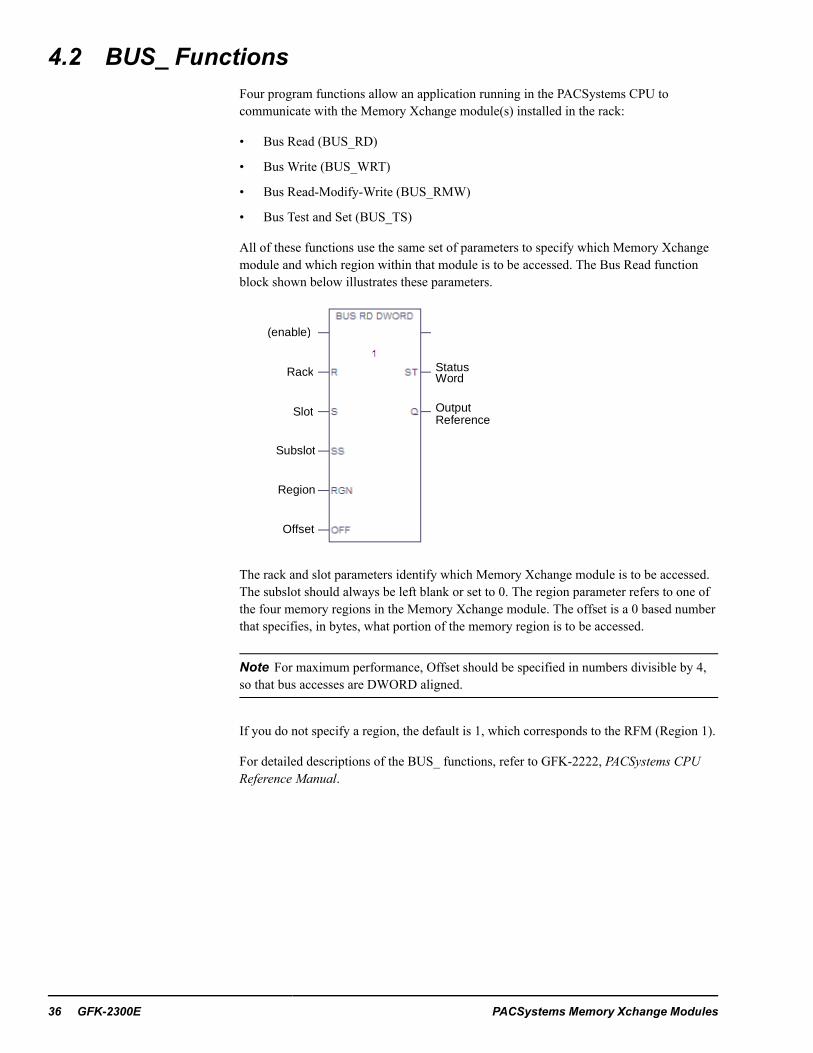
4.2 BUS_ FunctionsFour program functions allow an application running in the PACSystems CPU tocommunicate with the Memory Xchange module(s) installed in the rack:
• Bus Read (BUS_RD)
• Bus Write (BUS_WRT)
• Bus Read-Modify-Write (BUS_RMW)
• Bus Test and Set (BUS_TS)
All of these functions use the same set of parameters to specify which Memory Xchangemodule and which region within that module is to be accessed. The Bus Read functionblock shown below illustrates these parameters.
(enable)
Rack
Slot
Subslot
Region
Offset
StatusWord
OutputReference
The rack and slot parameters identify which Memory Xchange module is to be accessed.The subslot should always be left blank or set to 0. The region parameter refers to one ofthe four memory regions in the Memory Xchange module. The offset is a 0 based numberthat specifies, in bytes, what portion of the memory region is to be accessed.
Note For maximum performance, Offset should be specified in numbers divisible by 4,so that bus accesses are DWORD aligned.
If you do not specify a region, the default is 1, which corresponds to the RFM (Region 1).
For detailed descriptions of the BUS_ functions, refer to GFK-2222, PACSystems CPUReference Manual.
36 GFK-2300E PACSystems Memory Xchange Modules

4.2.1 Data Integrity of RMW and TS Bus AccessesRead-Modify-Write (RMW) accesses to Memory Xchange modules (via BUS_RMWorBUS_TS functions) are not guaranteed to be atomic with respect to accesses made tothese locations by the Memory Xchange module itself.
RMWaccesses across RX7i VME backplanes are atomic with respect to other busaccesses. Other bus masters will not be able to write to the module between the Read andthe Write operations. However, writes from the reflective memory network or theCMX/RMX module itself are not prevented. Thus, the bus write (of RMW) can overwriteand discard whatever data the network or module wrote to that same location.
RX3i backplane accesses are not guaranteed to be atomic with regard to other modules onthe backplane. However RX3i RMWaccess are atomic with respect to other backplaneaccesses made from that same CPU.
The BUS_TS_BYTE and BUS_TS_WORD functions can be used on the MemoryXchange modules, but they should not be used across the RFM (Region 1) between nodeson the network. Because the reflective memory network cannot be locked by any onenode at a given time, if the BUS_TS_* functions are simultaneously executed by twonodes, the function will incorrectly report that the semaphore was available for bothnodes. For additional information, see the description of the BUS_TS function block inGFK-2222, PACSystems CPU Reference Manual.
Basic Operation GFK-2300E User's Manual 37

4.3 Multiple Writes to Network MemoryApplications should be designed so that two or more nodes do not attempt to write to thesame reflective memory network address at the same time. If two or more nodes dohappen to write to the same address at approximately the same time, the values in thereflective memories on different nodes may become inconsistent.
For example, consider a four-node network consisting of Node 1, Node 2, Node 3 andNode 4 connected as shown below. If Node 1 writes 55h and Node 3 writes AAh tonetwork address 00h at approximately the same time, the following could occur:
• On Node 2, memory location 00h becomes 55h, but then is quickly changed to AAh.
• On Node 4 however, memory location 00h becomes AAh, but then is quicklychanged to 55h.
The net result is that Node 2 and Node 4 have different values at memory locations 00h.
3
21
455h
AAh
AAh
55h AAh
AAh
55h
55h
55h
AAh
Example of Multiple Writes to the Same RFM Network Location
If your application requires different nodes to write to the same network address, you canuse one of the following approaches to avoid writing to a memory location atapproximately the same time.
• Develop a set of rules for all nodes to follow that allow only one node to write to aparticular location at a time. For example, consider the simple case of two nodessharing one memory location. A set of rules could be:
− Node 1 can only write to the shared memory location when it already containsthe value 1 and can only write a value of 2.
− Node 2 can only write to that same location when it already contains the value 2and can only write a value of 1.
• Use network interrupts to signal when a particular memory location is available forwriting. For example:
− Node 1 initially has permission to write to location 0.− When Node 2 wants to write to location 0, it sends a network interrupt to Node 1
asking for permission.− When Node 1 receives that interrupt, it completes its write operations to location
0 if necessary, and then sends a network interrupt to Node 2 granting Node 2permission to write to location 0.
38 GFK-2300E PACSystems Memory Xchange Modules
4.4 Data Transfer TimeThe time to transfer data from one PLC to another via Memory Xchange modules ishighly dependent on your data exchange algorithm. However, the amount of time to writeand read data between a Memory Xchange module and a PACSystems CPU can becharacterized and is described in this section.
The following tables provide formulas for estimating the Read/Write time between aPACSystems CPU and a CMX module or an RMX module that is not being used as aredundancy link. Your actual read/write time may vary slightly from the estimated timeand most systems will see slightly better performance. The estimated Read/Write transfertimes are based on a CPU in a non-error condition without CPU serial communicationsactivity, Genius bus faults or other high backplane interrupt activity. In addition, thetiming is based on using single BUS_RD and BUS_WRT function blocks with data sizesfrom 256 to 131,068 bytes.
4.4.1 RX3i Read/Write Transfer TimesCPU to Memory Xchange Read/Write Transfer Time for CPU320 and CRU320
CPU Write to Memory Xchange Module Time (ms) = (0.000048 * (Number of Bytes)) +0.3480CPU Read from Memory Xchange Module Time (ms) = (0.000042 * (Number of Bytes))+ 0.3601
CPU to Memory Xchange Read/Write Transfer Time for CPU310
CPU Write to Memory Xchange Module Time (ms) = (0.000073 * (Number of Bytes)) +1.12CPU Read from Memory Xchange Module Time (ms) = (0.000094 * (Number of Bytes))+ 1.20
4.4.2 RX7i Read/Write Transfer TimesCPU to Memory Xchange Read/Write Transfer Time for CPE020 and CRE020
CPU Write to Memory Xchange Module Time (ms) = (0.00008079 * (Number of Bytes))+0.25CPU Read from Memory Xchange Module Time (ms) = (0.00006853 * (Number ofBytes))+0.22
CPU to Memory Xchange Read/Write Transfer Time for CPE010
CPU Write to Memory Xchange Module Time (ms) = (0.00009831 * (Number of Bytes))+0.644CPU Read from Memory Xchange Module Time (ms) = (0.00008468 * (Number ofBytes))+0.631
Basic Operation GFK-2300E User's Manual 39
4.4.3 Estimating Total Transfer TimeThe data transfer time over the fiber optic network is typically small compared to theRead/Write transfer time for most systems. Therefore, the total transfer time of one packetof data using a single BUS_WRT or BUS_RD function block can be roughly estimated byadding the CPU to Memory Xchange Read and Write times for a specific amount of dataand taking into account any asynchronous CPU delay time.
For example if you transferred 1024 bytes using the last DWORD (4 bytes) to signal validdata and the receiving CPU is running a sweep time of 5ms, you could use the followingsteps to estimate the data transfer time from one CPU to another.
Note The example uses CPE020/CRE020 timing values.
1. 1. Estimate write data time: WriteTime = (0.00008079 * (1024))+0.25 = 0.34 ms
2. 2. Estimate read data time (1024 bytes):ReadTime = (0.00006853 * (1024))+0.22 = 0.29 ms
3. 3. Estimate asynchronous CPU delay time. For most applications this will be oneCPU sweep time, since typical applications will check the Data Valid Dword onceper scan. However, this delay time could be much smaller if your applicationsynchronizes the CPUs prior to the data transfer operation.
AsyncDelayTime = Receiving CPU Scan time = 5 ms
4. 4. Estimate total transfer time:TotalTime = WriteTime + AsyncDelayTime + ReadTime
= 0.34 ms + 5 ms + 0.29 ms = 5.63 ms
Your algorithm may be more or less efficient than this example. For large data transfersyou may be able to optimize the data transfer by breaking the data transfers into smallerpackets so that one CPU reads a packet while the other CPU writes the next packet.
40 GFK-2300E PACSystems Memory Xchange Modules

4.5 Special Considerations for Stores of ConfigurationIf a hardware configuration containing changes to a Memory Xchange module isdownloaded, any changes your logic previously made to registers on that module could beoverwritten. Among other things, the following actions will occur:
• The module is temporarily disconnected from the network.
• The CPU clears the network interrupt FIFOs.
• The CPU clears the LIER.
• The CPU clears the LISR.
• The Latched Sync Loss bit (bit 3) in the module’s LCSR (offset 08h in region 2) isset ON (1).
• The module is reconnected to the network.
• A test packet is sent to determine whether all nodes on the ring are connected withtransmitters enabled. The OWN DATA status (bit 0) in the LCSR indicates whetheror not the ring is intact.
• The CONFIG LED (or LINK OK) is turned on.
If a hardware configuration is downloaded, but there is no change to a configured andoperational Memory Xchange module, the module remains connected to the network andtherefore continues to receive memory writes, etc. from other modules on the reflectivememory network. The CPU does not alter the registers on that module.
You can program the application logic to read the state of the Latched Sync Loss (bit 11)of the LISR on the first scan to determine whether the module was disconnected from thenetwork. If the module was disconnected, the data values in the reflective memories of allnodes in the network may need to be refreshed. To refresh the values, one or more nodeson the network should rewrite the desired values to reflective memory, that is, Region 1.
If a store changes the module’s network memory offset, the contents of the reflectivememory on that module are undefined after the store. You should refresh the values inRegion 1. To refresh the values, one or more nodes on the network should rewrite thedesired values to reflective memory.
Basic Operation GFK-2300E User's Manual 41

Notes
42 GFK-2300E PACSystems Memory Xchange Modules
5 Advanced Operation
Note The functions described in this chapter cannot be used on an RMX that is beingused as a redundancy link. When the Memory Xchange module is operating as acommunications link in a CPU redundancy system, these memory areas are under controlof the CPU and cannot be accessed by user logic. BUS_xxx accesses will fail with astatus value of 8 (Region not Enabled).
This chapter describes how to use the advanced capabilities of the Memory Xchangemodule. These functions are accessed via Regions 2, 3, and 4. Appendix B providesdetailed definitions of these regions. The advanced functions are:
• Module Interrupt Handling
• Network Interrupt Handling
• Memory Parity Checking
• On-demand Memory Clear
• Checking Ring Integrity
Advanced Operation GFK-2300E User's Manual 43
5.1 Module InterruptsThe Memory Xchange module has a single programmable module interrupt that can beused to trigger the execution of a block of logic. The Memory Xchange module cangenerate an interrupt for various events, such as Parity Error, Signal Detect Error, orRogue Packet fault. For a complete list refer to Chapter 5, the table, Module InterruptEvents.
If your application uses the module interrupt, it must write to the module to selectinterrupt sources and react to them when they occur. To control which events generate aninterrupt, write to the Local Interrupt Enable Register (LIER - Region 2, offset 14h).When the interrupt occurs, the logic must read the Local Interrupt Status Register (LISR –Region 2, offset 10h) to determine the reason(s) for the interrupt and respondappropriately.
Note If the module interrupt occurs while the CPU is in Stop mode, the associatedinterrupt block will not be executed for that occurrence.
Here is a summary of the steps involved in using module interrupts:
1. Decide which events you want to generate an interrupt. (Refer to chapter 5, thesection,Module Interrupt Events.)
2. Develop interrupt initialization logic.
3. Develop an interrupt handling logic block.
4. Set the Interrupt parameter for the module’s hardware configuration to Enabled.
5. Associate the interrupt with the logic block.
6. Store and test your application.
Module Interrupt Events
The Memory Xchange module can generate a module interrupt for any combination of thefollowing events. Use the LIER to select which of these events will cause an interrupt. Toactivate interrupts in an RX7i system, the Interrupt Enable (bit 14) of the LISR must alsobe set to 1.
Refer to Appendix B, Register Definitions for detailed definitions of these registers.
Module Interrupt Events
Event Description
Network Interrupt 1 A type 1 network interrupt was received.
Network Interrupt 2 A type 2 network interrupt was received.
Network Interrupt 3 A type 3 network interrupt was received.
Network Interrupt 4 A type 4 network interrupt was received.
Sync Loss The fiber optic receiver has lost the incoming signal. Data mayhave been prematurely removed from the network. Likely causesinclude: the configuration of this module was changed, the receivecable disconnected, or the upstream node’s transmitter wasdisabled (e.g. powered off, configuration changed, or explicitlydisabled).
44 GFK-2300E PACSystems Memory Xchange Modules
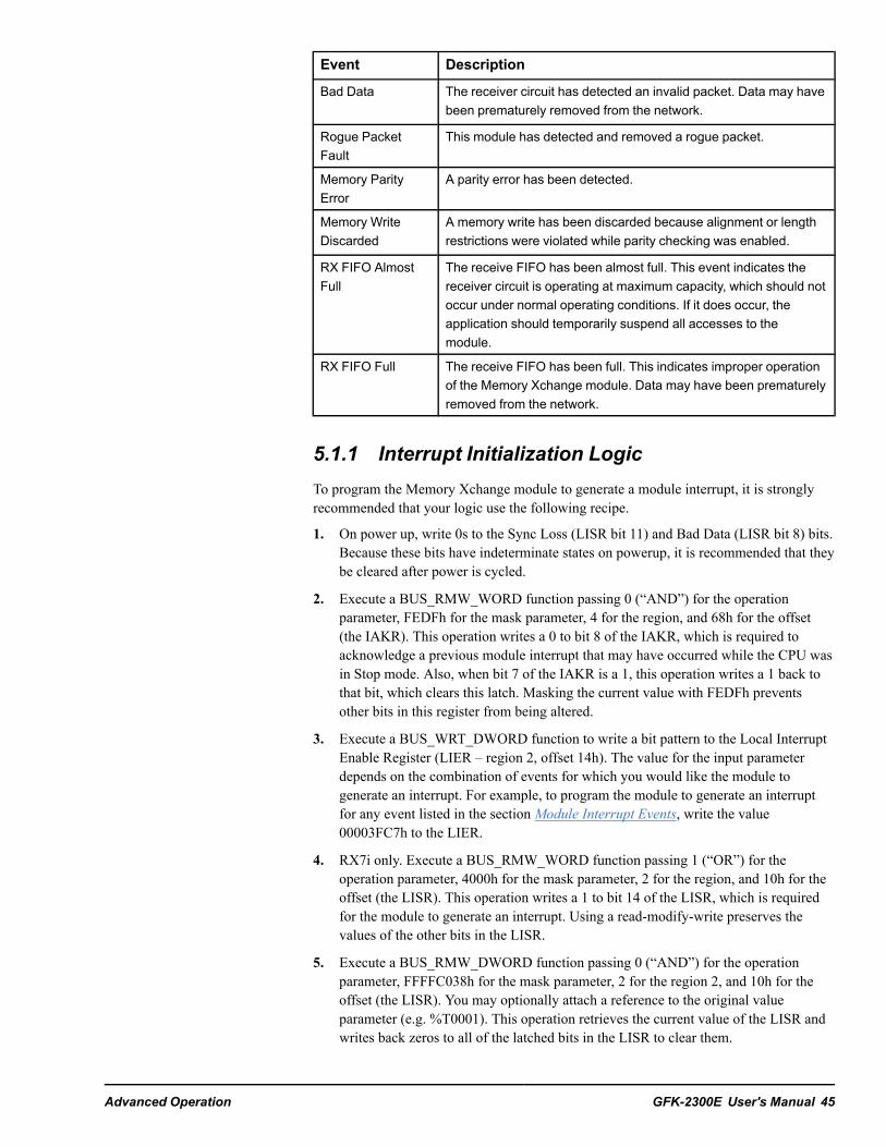
Event Description
Bad Data The receiver circuit has detected an invalid packet. Data may havebeen prematurely removed from the network.
Rogue PacketFault
This module has detected and removed a rogue packet.
Memory ParityError
A parity error has been detected.
Memory WriteDiscarded
A memory write has been discarded because alignment or lengthrestrictions were violated while parity checking was enabled.
RX FIFO AlmostFull
The receive FIFO has been almost full. This event indicates thereceiver circuit is operating at maximum capacity, which should notoccur under normal operating conditions. If it does occur, theapplication should temporarily suspend all accesses to themodule.
RX FIFO Full The receive FIFO has been full. This indicates improper operationof the Memory Xchange module. Data may have been prematurelyremoved from the network.
5.1.1 Interrupt Initialization LogicTo program the Memory Xchange module to generate a module interrupt, it is stronglyrecommended that your logic use the following recipe.
1. On power up, write 0s to the Sync Loss (LISR bit 11) and Bad Data (LISR bit 8) bits.Because these bits have indeterminate states on powerup, it is recommended that theybe cleared after power is cycled.
2. Execute a BUS_RMW_WORD function passing 0 (“AND”) for the operationparameter, FEDFh for the mask parameter, 4 for the region, and 68h for the offset(the IAKR). This operation writes a 0 to bit 8 of the IAKR, which is required toacknowledge a previous module interrupt that may have occurred while the CPU wasin Stop mode. Also, when bit 7 of the IAKR is a 1, this operation writes a 1 back tothat bit, which clears this latch. Masking the current value with FEDFh preventsother bits in this register from being altered.
3. Execute a BUS_WRT_DWORD function to write a bit pattern to the Local InterruptEnable Register (LIER – region 2, offset 14h). The value for the input parameterdepends on the combination of events for which you would like the module togenerate an interrupt. For example, to program the module to generate an interruptfor any event listed in the section Module Interrupt Events, write the value00003FC7h to the LIER.
4. RX7i only. Execute a BUS_RMW_WORD function passing 1 (“OR”) for theoperation parameter, 4000h for the mask parameter, 2 for the region, and 10h for theoffset (the LISR). This operation writes a 1 to bit 14 of the LISR, which is requiredfor the module to generate an interrupt. Using a read-modify-write preserves thevalues of the other bits in the LISR.
5. Execute a BUS_RMW_DWORD function passing 0 (“AND”) for the operationparameter, FFFFC038h for the mask parameter, 2 for the region 2, and 10h for theoffset (the LISR). You may optionally attach a reference to the original valueparameter (e.g. %T0001). This operation retrieves the current value of the LISR andwrites back zeros to all of the latched bits in the LISR to clear them.
Advanced Operation GFK-2300E User's Manual 45
6. Optional. Test each non-network interrupt status bit in the local copy of the LISR.For example, if the value of bit 11 (for example, %T0011) is a 1, a sync losscondition occurred before the logic in Step 5 was run.
7. Optional: For each of the four network interrupt bits (0, 1, 2, and 7) in the LISR:
a. Test the network bit in the local copy of the LISR (for example, test %T0001 fortype 1 network interrupts). If the bit is a 1, read the corresponding networkinterrupt FIFO.
b. Optional: Execute a BUS_READ_DWORD function to read the LISR (region 2,offset 10h) again. It is important to not write any values back to the LISR afterStep 5. Then repeat Step 7.
8. Execute a BUS_RMW_BYTE function passing 1 (“OR”) for the operationparameter, 1 for the mask parameter, 4 for the region, and 69h for the offset (theIAKR). This operation writes a 1 to bit 8 of the IAKR, which allows the module togenerate a module interrupt. Using an OR operation with the value of 1 preventsother bits in this register from being altered. If at this moment, a bit in the LISR is a 1and its corresponding bit in the LIER is also a 1, the module immediately generates amodule interrupt. In this case, the CPU schedules your interrupt block for execution.
5.1.2 Interrupt Handling LogicWhen developing the logic for an interrupt block that will handle the module interruptfrom a Memory Xchange module, it is strongly recommended that you use the followingrecipe.
Caution
If the steps in the following procedure are not followedcompletely, unexpected results, such as unacknowledgedinterrupts, can occur or the Watchdog Timer can trip.
You should configure only one interrupt block toacknowledge a Memory Xchange module interrupt.Assigning multiple interrupt blocks to be executed fromthe same module can lead to unpredictable andundesirable results, including tripping of the softwarewatchdog. Only one module interrupt block can includethe Interrupt Handling Logic recipe described below.
1. Execute a BUS_RMW_WORD function passing 0 (“AND”) for the operationparameter, FEDFh for the mask parameter, 4 for the region, and 68h for the offset(the IAKR). This operation writes a 0 to bit 8 of the IAKR, which is required toacknowledge the module interrupt. Also, when bit 7 of the IAKR is a 1, thisoperation writes a 1 back to that bit, which clears this latch. Masking the currentvalue with FEDFh prevents other bits in this register from being altered.
2. Execute a BUS_RMW_DWORD function passing 0 (“AND”) for the operationparameter, FFFFC038h for the mask parameter, 2 for the region, and 10h for theoffset (the LISR). Attach a reference to the original value parameter (e.g. %T0001).This operation retrieves the current value of the LISR and writes back zeros to all ofthe latched bits to clear them.
3. Test each non-network interrupt status bit in the local copy of the LISR. For example,if the value of bit 11 (e.g. %T0011) is a 1, a sync loss condition occurred.
4. For each of the four possible network interrupt bits in the LISR (bits 0, 1, 2, and 7):
46 GFK-2300E PACSystems Memory Xchange Modules
a. Test the network bit in the local copy of the LISR (e.g. test %T0001 for type 1network interrupts). If the bit is a 1, read the corresponding network interruptFIFO.
b. Optional: Execute a BUS_RD_DWORD function to read the LISR (region 2,offset 10h) again. It is important to not write any values back to the LISR afterStep 2. Then repeat Step 4.
5. Execute a BUS_RMW_BYTE function passing 1 (“OR”) for the operationparameter, 1 for the mask parameter, 4 for the region, and 69h for the offset (theIAKR). This operation writes a 1 to bit 8 of the IAKR, which allows the module togenerate another module interrupt. Using an “OR” operation with the value of 1prevents other bits in this register from being altered. If at this moment, a bit in theLISR is a 1 and its corresponding bit in the LIER is also a 1, the module immediatelygenerates another module interrupt. In this case, the CPU schedules the interruptblock for an additional execution.
5.1.3 Associating Module Interrupts with LogicWhen using interrupts from the Memory Xchange module to trigger logic execution, anassociation between the interrupt and the logic block to be executed must be specified.Before you can create this association, the module generating the interrupt must beconfigured in the hardware configuration and its Interrupt parameter must be set toEnabled.
In Machine Edition software, display the properties of the interrupt logic block, andexpand the Scheduling property. In the Scheduling dialog box, select Module Interrupt forthe Type. For the Trigger, use the dropdown list to select a module interrupt. The moduleis identified as r.s (#i), where r is the rack, s is the slot, and #i is the interrupt number. Useinterrupt #1.
Caution
You should configure only one interrupt block toacknowledge a Memory Xchange module interrupt.Assigning multiple interrupt blocks to be executed fromthe same module can lead to unpredictable andundesirable results, including tripping of the softwarewatchdog. Only one module interrupt block can includethe Interrupt Handling Logic recipe described onChapter 5, the section, Interrupt Handling Logic.
Advanced Operation GFK-2300E User's Manual 47

5.1.4 Dynamic Masking of Module Interrupts
5.1.4.1 At the Memory Xchange Module
RX7i Memory Xchange Modules
The application program can mask and unmask the module interrupt from a MemoryXchange module at run time by writing to the Interrupt Enable (bit 14) of the LISR.
RX3i Memory Xchange Modules
To mask interrupts on the RX3i you must perform a BUS_RMW_BYTE passing 0 (AND)for the operation and 0xFE for the mask, 4 for the region, and 0x69 for the offset.
To unmask interrupts on the RX3i you must perform a BUS_RMW_BYTE passing 1(OR) for the operation and 0x01 for the mask, 4 for the region, and 0x69 for the offset.
5.1.4.2 At the CPU (RX7i Only)
The application program can mask and unmask the execution of the interrupt blockassociated with a Memory Xchange module at run time by using the SVC_REQ functionblock 17. To use SVC_REQ 17 with a Memory Xchange module, pass 17 decimal as thememory type and the VME interrupt id as the offset. To obtain an RX7i module’s VMEinterrupt ID, refer to GFK 2235, PACSystems RX7i User’s Guide to Integration of VMEModules.
When the execution of the interrupt block is not masked, the CPU processes the VME businterrupt and schedules the associated logic block for execution. When the execution ofthe interrupt block is masked, the CPU processes the module interrupt but will notschedule the associated logic block for execution (i.e., it discards that interrupt).Whenever the CPU transitions from Stop to Run, the execution of the interrupt block isunmasked.
For details on using SVC_REQ #17, refer to GFK-2222, PACSystems CPU ReferenceManual.
Note The RX3i controller does not support masking of module interrupts (such as thatgenerated by the IC695CMX128 module) using SVC_REQ 17.
48 GFK-2300E PACSystems Memory Xchange Modules

5.2 Network InterruptsAny node on the network can send a network interrupt packet to a specific node on thenetwork or broadcast it globally to all nodes on the network. Each network interruptpacket contains the sender’s node ID, the target (destination) node ID, the interrupt typeinformation, and 32 bits of user defined data. There are four types of network interrupts,all of which are user-defined.
5.2.1 Sending Network InterruptsTo initiate a network interrupt, your application logic must write to three registers ofRegion 2:
1. Write 32 bits of user defined data to the Network Target Data (NTD) register.
2. Write the destination node id to the Network Target Node (NTN) register.
3. Write interrupt Type information to the Network Interrupt Command (NIC) register.This step must be executed last since it actually generates the network interruptpacket. To determine the value to write to this register, refer to Appendix B.
Steps 2 and 3 can be accomplished with one BUS_WRT_WORD function.
5.2.2 Receiving Network InterruptsEach time a node issues a network interrupt, it includes its own node ID as part of thepacket. When the Memory Xchange module receives a network interrupt that is directedto it, it stores the sender’s node ID and the 32 bits of user defined data in a FIFO (first infirst out) queue. There is a separate FIFO for each of the four network interrupt types (1–4).
Queue depth, or the number of interrupts each FIFO can store, is as follows:
RX7i CMX and RMX modules: 127 interrupts
RX3i CMX and RMX modules: 130 interrupts
Any time at least one entry is pending in a FIFO, the corresponding bit in the LISR is setto 1. Optionally, the module can be programmed to generate a module interrupt uponreceipt of a network interrupt.
To retrieve the oldest entry in the FIFO, the application logic should do the following.
1. Read the corresponding Interrupt Send Data (ISDx) register.
2. Read the corresponding Interrupt Sender Node ID (SIDx) register.
When the SIDx register is read, the entire entry (Node ID and user data) is removed fromthe FIFO. Therefore, each sender node ID can only be read once. If the sender data isdesired, read the corresponding Interrupt Sender Data (ISDx) register before reading theInterrupt Sender Node ID (SIDx) register.
Advanced Operation GFK-2300E User's Manual 49

5.2.2.1 Initialization
If your application will service network interrupts using an interrupt block, you shoulduse the recipe described in Chapter 5, the section, Interrupt Initialization Logic.
If your application needs to discard any unserviced network interrupts, clear eachInterrupt Sender ID (SID) FIFO by writing a one-byte 0 to the following offsets of Region2:
Sender ID FIFO OffsetSID1 24h
SID2 2Ch
SID3 34h
SID4 3Ch
5.2.2.2 Servicing Network Interrupts
The following recipe demonstrates the steps necessary to service all four networkinterrupt FIFOs. All registers accessed in this recipe are in region 2.
Note If your application detects the receipt of a network interrupt using an interruptblock, you should include this recipe inside the one described in Chapter 5, the section,Interrupt Handling Logic.
1. Obtain the value of the LISR. For example, execute a BUS_READ_DWORDfunction passing 2 for the region 2 and 10h for the offset. Attach a reference to theoutput parameter (for example, %T0001). It is important to not write any values backto the LISR.
2. If all four Network Interrupt bits (0, 1, 2, and 7) of the LISR are 0, no interrupts arepending and you can exit this procedure.
3. Test bit 0 (e.g. %T0001) of the LISR. If the bit is a 1, a type 1 network interrupt ispending.
a. Read the Interrupt 1 Sender Data (ISD1) register (offset 20h) to retrieve the 32bits of data.
b. Read the Interrupt 1 Sender Node ID (SID1) register (offset 24h) to retrieve thesender’s node ID.
4. Test bit 1 (for example, %T0002) of the LISR. If the bit is a 1, a type 2 networkinterrupt is pending.
a. Read the Interrupt 2 Sender Data (ISD2) register (offset 28h) to retrieve the 32bits of data.
b. Read the Interrupt 2 Sender Node ID (SID2) register (offset 2Ch) to retrieve thesender’s node ID.
5. Test bit 2 (for example, %T0003) of the LISR. If the bit is a 1, a type 3 networkinterrupt is pending.
a. Read the Interrupt 3 Sender Data (ISD3) register (offset 30h) to retrieve the 32bits of data.
50 GFK-2300E PACSystems Memory Xchange Modules

b. Read the Interrupt 3 Sender Node ID (SID3) register (offset 34h) to retrieve thesender’s node ID.
6. Test bit 7 (e.g. %T0008) of the LISR. If the bit is a 1, a type 4 network interrupt ispending.
a. Read the Interrupt 4 Sender Data (ISD4) register (offset 38h) to retrieve the 32bits of data.
b. Read the Interrupt 4 Sender Node ID (SID4) register (offset 3Ch) to retrieve thesender’s node ID.
7. Optional. To check for and service additional pending interrupts, repeat this entireprocess starting with Step 1.
5.3 Memory Parity CheckingIf your application requires the use of memory parity checking on the Memory Xchangemodule, the application must write to the module to enable parity and react to any parityerrors (for example, logging a user application fault). To enable parity checking, write a 1to bit 27 of the Local Control and Status Register (LCSR – Region 2, offset 8h). You canoptionally program the module to generate a module interrupt for parity errors (refer tothe section,Module Interrupts).
When parity checking is enabled, all writes to region 1 must occur on Dword (32-bit)boundaries. While parity checking is active, byte (8-bit) and word (16-bit) writes toRegion 1 are prohibited. If such a write is attempted, the BUS_ function will appear tocomplete successfully; however, the contents of the memory location will not change. Themodule reports this error by setting the Memory Write Discarded bit (bit 12) of the LocalInterrupt Status Register (LISR - Region 2, offset 10h) to 1. The Memory Xchangemodule also sets the Memory Write Discarded bit to 1 when an invalid memory write isreceived from the reflective memory network.
Before enabling its transmitter, the module initializes all of Region 1 to 0 at power up.This action initializes the parity bits for all of the reflective memory on that module.
If you enable parity checking on one node, you should enable it on all nodes of thereflective memory network. (A node that detects an invalid memory write from thenetwork will prevent the write to its own memory, but it will not remove the packet fromthe network.)
The following table highlights the bits used for the parity checking function.
Note When setting or clearing the bits described below, it is recommended that you usethe BUS_RMW instruction so that other bits in the same register are not affected.
Local Control and Status Register (LCSR), Region 2 offset 08h
Name Bit Description
Parity Checking Enable Bit27
When set to 1, memory parity checking is enabled.
Advanced Operation GFK-2300E User's Manual 51

Local Interrupt Status Register (LISR), Region 2 offset 10h
Name Bit Description
LISR Parity Error Latch Bit13
When set to 1, a parity error has been detected. Writea 0 to this bit to clear it.For RX7i systems, always clear bit 7 of the IAKRregister before clearing this bit.
Memory WriteDiscarded
Bit12
When set to 1, a memory write has been discardedbecause alignment or length restrictions were violatedwhile parity checking was enabled. Write a 0 to this bitto clear it.
Interrupt Acknowledge Register (IAKR), Region 4 offset 68h
Name Bit Description
IAKR Parity Error Latch Bit 7 RX7i only: When set to 1, a parity error has beendetected. Write a 1 to this bit to clear it. Always clearthis bit before clearing bit 13 of the LISR.RX3i: Reserved
5.3.1 Logic for Detecting and Clearing a Parity ErrorIf your application detects and clears parity errors using an interrupt block, you shoulduse the recipe described in Chapter 5, the section, Interrupt Handling Logic to clear theParity Error latches.
Otherwise, use the following recipe to detect and clear the Parity Error latches. You maywant to execute this logic at a rate of once per sweep.
1. Execute a BUS_RMW_BYTE function passing 0 (“AND”) for the operationparameter, DFh for the mask parameter, 4 for the region, and 68h for the offset (theIAKR). When bit 7 of the Interrupt Acknowledge Register is a 1, this operationwrites a 1 back to that bit, which clears this latch. Masking the current value withDFh prevents other bits in this register from being altered.
2. Execute a BUS_RMW_DWORD function passing 0 (“AND”) for the operationparameter, FFFFDFFFh for the mask parameter, 2 for the region, and 10h for theoffset (the LISR). Attach a reference to the original value parameter (for example, %T0001). This operation retrieves the current value of the LISR and writes a zero backto bit 13 to clear it. (A different mask value, such as FFFFC038h, can be used if youwish to clear other bits of the LISR at this time.)
3. Test the value of bit 13 in the local copy of the LISR (for example, %T0013). If thevalue of this bit is a 1, a memory parity error occurred.
52 GFK-2300E PACSystems Memory Xchange Modules

5.4 On-demand Memory ClearThe Memory Xchange module supports a command that writes 0s to all locations inRegion 1. As long as the transmitter is enabled, these writes are also sent to the network.The operation could take several seconds to complete. While executing this command, themodule defers generation of module interrupts.
• To initiate the command, execute a BUS_RMW_BYTE function passing 1 (OR) forthe Operation parameter, 4h for the Mask parameter, 3 for the Region parameter, and442h for the Offset.
• To determine when the memory clear is complete, execute a BUS_RD_BYTEfunction passing 3 for the Region parameter and 442h for the Offset. When ClearMemory (bit 2) is 0, the operation is complete.
Before initiating another clear, ensure the previous one is complete.
5.5 Checking Ring IntegrityAt any time you may check the integrity of the ring by initiating a data packet andverifying that it has returned. This indicates whether or not all nodes on the ring areconnected with transmitters enabled.
To check the ring, do the following:
1. Clear the OWN DATA status bit by executing a BUS_RMW_BYTE function passing0 (AND) for the Operation parameter, FEh for the Mask parameter, 2 for the Regionparameter, and 8h for the Offset.
2. Initiate a network packet by writing to Region 1 or generating a network interrupt.
3. Read the LCSR (Region 2 – offset 08h) by executing a BUS_RD_BYTE.
4. Test the OWN DATA status (bit 0).
5. Repeat from step 2 until the OWN DATA bit becomes 1, which means the ring isintact.
Advanced Operation GFK-2300E User's Manual 53
5.6 Optimizing Network BandwidthThe maximum bandwidth of the reflective memory network ranges from 43 Mbytes/s to174 Mbytes/s. A network’s effective bandwidth is determined by the efficiency of packetsizing. Each packet sent over the network includes, in addition to the data, a fixed numberof overhead bytes that tell each node where and how to store the data. More bytes of dataper packet compared to the fixed overhead bytes results in a higher data rate.
The user has no direct control over the packet size. The Memory Xchange moduledynamically sizes the packets on the network based on the manner in which they werefirst written into reflective memory by the source node. To optimize packet length andeffective network bandwidth, nodes on the network should transfer data in bursts ofsequential addressed data.
Using individual writes and reads to transfer data should be avoided. If all nodes on thenetwork transfer data in a fully random access manner, minimum packet sizes will alwaysresult and the 43 Mbyte/s data rate will dominate the entire network.
The effect of the Redundant Transfer mode (discussed in chapter 2) on network data ratemust also be considered. When a CMX or RMX module is placed in Redundant Transfermode, each packet it generates is sent twice over the network. This improves thestatistical reliability of the system. However, it also reduces the effective network transferrate by more than half. For a CMX/RMX system, the effective transfer rate in RedundantTransfer mode will vary from 20 Mbyte/s to 70 Mbyte/s.
To avoid degradation of network performance or the possibility of losing data, theapplication must avoid a situation where the transmit FIFO becomes full. The RX FIFOAlmost Full status bit (bit 09) in the LISR (Region 2, offset 10h) can be monitored todetermine if the network is becoming saturated.
54 GFK-2300E PACSystems Memory Xchange Modules

5.6.1 Using Network Interrupts to Balance NetworkLoadTo avoid filling the transmit FIFOs, you can use network interrupts to allow only part ofthe nodes on a network to transmit at the same time.
Example
The sample network consists of a 20-node PLC-style scanning system, with nodesnumbered 0 to 19. Scan time is 10ms. Redundant Transfer mode is disabled.
Each node is capable of transmitting data on the network at approximately 40 Mbyte/s. Ifall 20 nodes transmit at the same time, the attempted data rate is 800 Mbyte/s. Thissignificantly exceeds the maximum network bandwidth and will cause the FIFOs to fillup.
Network interrupts can be used to synchronize the nodes and distribute the network trafficthroughout the 10 ms scan.
For this example, pick node 0 to be the master. The master will divide the 10 ms scan intofive subintervals of 2 ms each, numbered 0 – 4. Each PLC node will finish writing datawhen its 2 ms window is completed. Assign each node to a subinterval, distributing thenodes evenly between subintervals.
For this example, the nodes are assigned as follows:
Nodes SubintervalNodes 0, 5, 10, 15 subinterval 0
Nodes 1, 6, 11, 16 subinterval 1
Nodes 2, 7, 12, 17 subinterval 2
Nodes 3, 8, 13, 18 subinterval 3
Nodes 4, 9, 14, 19 subinterval 4
The user-defined data associated with the interrupt contains the value of the currentsubinterval (0 – 4). Each node waits for the network interrupt, and when the interrupt dataequals the subinterval it is assigned, it writes its data. During each 2 ms subinterval, onlyfour nodes are transmitting at the same time. For example, during subinterval 0, nodes 0,5, 10 and 15 write their data. This limits the peak network data rate to 40 Mbyte/s * 4 =160 Mbyte/s, which is less than the maximum network bandwidth of 174 Mbyte/s.
Advanced Operation GFK-2300E User's Manual 55

Notes
56 GFK-2300E PACSystems Memory Xchange Modules
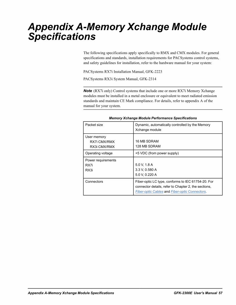
Appendix A-Memory Xchange ModuleSpecifications
The following specifications apply specifically to RMX and CMX modules. For generalspecifications and standards, installation requirements for PACSystems control systems,and safety guidelines for installation, refer to the hardware manual for your system:
PACSystems RX7i Installation Manual, GFK-2223
PACSystems RX3i System Manual, GFK-2314
Note (RX7i only) Control systems that include one or more RX7i Memory Xchangemodules must be installed in a metal enclosure or equivalent to meet radiated emissionstandards and maintain CE Mark compliance. For details, refer to appendix A of themanual for your system.
Memory Xchange Module Performance Specifications
Packet size Dynamic, automatically controlled by the MemoryXchange module
User memoryRX7i CMX/RMXRX3i CMX/RMX
16 MB SDRAM128 MB SDRAM
Operating voltage +5 VDC (from power supply)
Power requirementsRX7iRX3i
5.0 V, 1.8 A3.3 V, 0.580 A5.0 V, 0.220 A
Connectors Fiber-optic LC type, conforms to IEC 61754-20. Forconnector details, refer to Chapter 2, the sections,Fiber-optic Cables and Fiber-optic Connectors.
Appendix A-Memory Xchange Module Specifications GFK-2300E User's Manual 57

Notes
58 GFK-2300E PACSystems Memory Xchange Modules

Appendix B-Register DefinitionsThis appendix gives detailed definitions of the module’s registers:
Region 2: Primary Control and Status Registers
Region 3: Auxiliary Control and Status Registers
Region 4: Interrupt Acknowledge Registers
Note When the RMX module is operating as a redundancy link, these memory areas areunder control of the CPU and cannot be accessed by user logic. BUS_xxx accesses willfail with a status value of 8 (Region not Enabled).
Note When modifying individual bits of these registers, it is recommended that you usethe BUS_RMW instruction so that other bits in the same register are not affected.
Appendix B-Register Definitions GFK-2300E User's Manual 59

Region 2: Primary Control and Status RegistersOffset(hex)
Mnemonic Description Access Comments
00h–03h — Reserved — Do not modify.
04h NID Node ID Register ReadOnly
Reflects the Node ID set by the hardware configuration.
05–07h — Reserved — Do not modify.
08–0Bh LCSR Local Control AndStatus Register
Read/-Write
Some bits reserved. Some bits read only. For details,refer to the table Local Control and Status Register BitDefinitions.
0C–0Fh — Reserved — Do not modify.
10–13h LISR Local Interrupt StatusRegister
Read/-Write
Some bits reserved. Some bits read only. For details,refer to the table Local Interrupt Status Register BitDefinitions.
14–17h LIER Local InterruptEnable Register
Read/-Write
Some bits reserved. Some bits read only. For details,refer to the table LIER Bit Defiinitions.
18–1Bh NTD Network Target Data Read/-Write
Data bits for network interrupt. For details, refer to thesection Registers for Generating Network Interrupts.
1Ch NTN Network Target Node Read/-Write
Target node ID for network interrupt. For details, refer tothe section Registers for Generating Network Interrupts.
1Dh NIC Network InterruptCommand
Read/-Write
Initiate network interrupt. For details, refer to the sectionRegisters for Generating Network Interrupts.
1E–1Fh — Reserved — Do not modify.
20–23h ISD1 Interrupt 1 SenderData
Read/-Write
Read user defined data from FIFO for network interrupt1. For details, refer to the section Registers forGenerating Network Interrupts.
24h SID1 Interrupt 1 SenderNode ID
Read/-Write
Read Node ID from FIFO for network interrupt 1. Fordetails, refer to the section Registers for GeneratingNetwork Interrupts.
25–27h — Reserved — Do not modify.
28–2Bh ISD2 Interrupt 2 SenderData
Read/-Write
Read user defined data from FIFO for network interrupt2. For details, refer to the section Registers forGenerating Network Interrupts.
2Ch SID2 Interrupt 2 SenderNode ID
Read/-Write
Read Node ID from FIFO for network interrupt 2. Fordetails, refer to the section Registers for GeneratingNetwork Interrupts.
2D–2Fh — Reserved — Do not modify.
30h-33h ISD3 Interrupt 3 SenderData
Read/-Write
Read user defined data from FIFO for network interrupt3. For details,refer to the section Registers forGenerating Network Interrupts.
34h SID3 Interrupt 3 SenderNode ID
Read/-Write
Read Node ID from FIFO for network interrupt 3. Fordetails, refer to the section Registers for GeneratingNetwork Interrupts.
60 GFK-2300E PACSystems Memory Xchange Modules

Offset(hex)
Mnemonic Description Access Comments
35–37h — Reserved — Do not modify.
38–3Bh ISD4 Interrupt 4 SenderData
Read/-Write
Read user defined data from FIFO for network interrupt4. For details, refer to the section Registers forGenerating Network Interrupts.
3Ch SID4 Interrupt 4 SenderNode ID
Read/-Write
Read Node ID from FIFO for network interrupt 4. Fordetails, refer to the section Registers for GeneratingNetwork Interrupts.
3D-FFFh — Reserved — Do not modify.
Local Control and Status Register (LCSR)Offset 08h, Read/Write, Dword, Word, Byte
Bit 07 Bit 06 Bit 05 Bit 04 Bit 03 Bit 02 Bit 01 Bit 00
TX FIFOEmpty
TX FIFOAlmost Full
Latched RXFIFO Full
Latched RXFIFO AlmostFull
Sync Loss RX SignalDetect
Bad Data Own Data
Bit 15 Bit 14 Bit 13 Bit 12 Bit 11 Bit 10 Bit 09 Bit 08
Reserved
Bit 23 Bit 22 Bit 21 Bit 20 Bit 19 Bit 18 Bit 17 Bit 16
Reserved
Bit 31 Bit 30 Bit 29 Bit 28 Bit 27 Bit 26 Bit 25 Bit 24
Reserved ParityCheckingEnable
RedundantTransferModeEnabled
RogueMaster 1Enabled
RogueMaster 0Enabled
Local Control and Status Register Bit Definitions
Bit(s) Name Access Description
Bit 00 Own Data Read/Write When this bit is set to 1, the module has detected the return of its own dataor interrupt packet at least once since this bit was cleared. This bit alsocontrols the state of the OWN DATA LED. Write a 0 to this bit to clear it.
Bit 01 Bad Data Read Only When this bit is set to 1, the receiver circuit has detected an invalid packet.Data may have been prematurely removed from the network. To clear thisbit, write to bit 08 in the LISR.On powerup, this bit has an indeterminate state. It is recommended that thisbit be cleared after power is cycled.
Bit 02 RX SignalDetect
Read Only When this bit is set to 1, the module receiver is currently detecting light. Thisbit provides immediate status only (not latched).
Bit 03 Sync Loss Read Only When this bit is set to 1, the fiber optic receiver has lost the incoming signalat least once since the last time the corresponding bit in the LISR wascleared. Data may have been prematurely removed from the network. Likelycauses include the configuration of this module was changed, the receive
Appendix B-Register Definitions GFK-2300E User's Manual 61
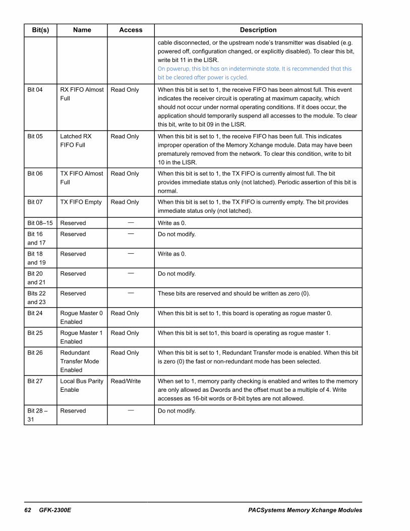
Bit(s) Name Access Description
cable disconnected, or the upstream node’s transmitter was disabled (e.g.powered off, configuration changed, or explicitly disabled). To clear this bit,write bit 11 in the LISR.On powerup, this bit has an indeterminate state. It is recommended that thisbit be cleared after power is cycled.
Bit 04 RX FIFO AlmostFull
Read Only When this bit is set to 1, the receive FIFO has been almost full. This eventindicates the receiver circuit is operating at maximum capacity, whichshould not occur under normal operating conditions. If it does occur, theapplication should temporarily suspend all accesses to the module. To clearthis bit, write to bit 09 in the LISR.
Bit 05 Latched RXFIFO Full
Read Only When this bit is set to 1, the receive FIFO has been full. This indicatesimproper operation of the Memory Xchange module. Data may have beenprematurely removed from the network. To clear this condition, write to bit10 in the LISR.
Bit 06 TX FIFO AlmostFull
Read Only When this bit is set to 1, the TX FIFO is currently almost full. The bitprovides immediate status only (not latched). Periodic assertion of this bit isnormal.
Bit 07 TX FIFO Empty Read Only When this bit is set to 1, the TX FIFO is currently empty. The bit providesimmediate status only (not latched).
Bit 08–15 Reserved — Write as 0.
Bit 16and 17
Reserved — Do not modify.
Bit 18and 19
Reserved — Write as 0.
Bit 20and 21
Reserved — Do not modify.
Bits 22and 23
Reserved — These bits are reserved and should be written as zero (0).
Bit 24 Rogue Master 0Enabled
Read Only When this bit is set to 1, this board is operating as rogue master 0.
Bit 25 Rogue Master 1Enabled
Read Only When this bit is set to1, this board is operating as rogue master 1.
Bit 26 RedundantTransfer ModeEnabled
Read Only When this bit is set to 1, Redundant Transfer mode is enabled. When this bitis zero (0) the fast or non-redundant mode has been selected.
Bit 27 Local Bus ParityEnable
Read/Write When set to 1, memory parity checking is enabled and writes to the memoryare only allowed as Dwords and the offset must be a multiple of 4. Writeaccesses as 16-bit words or 8-bit bytes are not allowed.
Bit 28 –31
Reserved — Do not modify.
62 GFK-2300E PACSystems Memory Xchange Modules

Local Interrupt Status Register (LISR)Offset 10h, Read/Write, Dword, Word, Byte
Bit 07 Bit 06 Bit 05 Bit 04 Bit 03 Bit 02 Bit 01 Bit 00
NetworkInterrupt 4Flag
RoguePacket Fault
Reserved NetworkInterrupt 3Flag
NetworkInterrupt 2Flag
NetworkInterrupt 1Flag
Bit 15 Bit 14 Bit 13 Bit 12 Bit 11 Bit 10 Bit 09 Bit 08
RX7i: AutoClear Flag
RX7i:InterruptEnable
LISR ParityError Latch
MemoryWriteDiscarded
Sync Loss RX FIFO Full RX FIFOAlmost Full
Bad Data
RX3i Reserved
Bit 23 Bit 22 Bit 21 Bit 20 Bit 19 Bit 18 Bit 17 Bit 16
Reserved
Bit 31 Bit 30 Bit 29 Bit 28 Bit 27 Bit 26 Bit 25 Bit 24
Reserved
Local Interrupt Status Register Bit Definitions
Bit(s) Name Access Description
Bit 00 NetworkInterrupt 1 Flag
— When this bit is a 1, at least one type 1 network interrupt is pending in thecorresponding FIFOs. This bit remains a 1 until the Interrupt 1 Sender NodeID (SID1) FIFO becomes empty.
Bit 01 NetworkInterrupt 2 Flag
— When this bit is a 1, at least one type 2 network interrupt is pending in thecorresponding FIFOs. This bit remains a 1 until the Interrupt 2 Sender NodeID (SID2) FIFO becomes empty.
Bit 02 NetworkInterrupt 3 Flag
— When this bit is a 1, at least one type 3 network interrupt is pending in thecorresponding FIFOs. This bit remains a 1 until the Interrupt 3 Sender NodeID (SID3) FIFO becomes empty.
Bit 03–05 Reserved — Do not modify.
Bit 06 Rogue PacketFault
Read/Write When this bit is a 1, the module has detected and removed a rogue packet.This bit is latched. Once set, it must be cleared by writing a zero to this bitlocation.
Bit 07 NetworkInterrupt 4 Flag
— When this bit is a 1, at least one type 4 network interrupt is pending in thecorresponding FIFOs. This bit remains a 1 until the Interrupt 4 Sender NodeID (SID4) FIFO becomes empty.
Bit 08 Bad Data Read/Write Read/Write When this bit is a 1, The receiver circuit has detected an invalidpacket. Data may have been prematurely removed from the network. Thisbit is latched. Once set, it must be cleared by writing a zero to this bitlocation.
Bit 9 RX FIFOAlmost Full
Read/Write When this bit is a 1, The receive FIFO has been almost full. This eventindicates the receiver circuit is operating at maximum capacity, whichshould not occur under normal operating conditions. If it does occur, theapplication should temporarily suspend all accesses to the module. Onceset, it must be cleared by writing a zero to this bit location.
Appendix B-Register Definitions GFK-2300E User's Manual 63
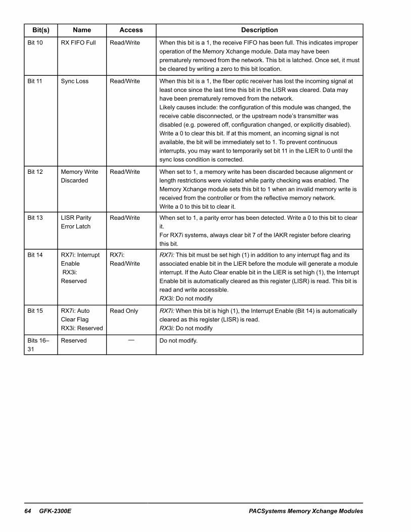
Bit(s) Name Access Description
Bit 10 RX FIFO Full Read/Write When this bit is a 1, the receive FIFO has been full. This indicates improperoperation of the Memory Xchange module. Data may have beenprematurely removed from the network. This bit is latched. Once set, it mustbe cleared by writing a zero to this bit location.
Bit 11 Sync Loss Read/Write When this bit is a 1, the fiber optic receiver has lost the incoming signal atleast once since the last time this bit in the LISR was cleared. Data mayhave been prematurely removed from the network.Likely causes include: the configuration of this module was changed, thereceive cable disconnected, or the upstream node’s transmitter wasdisabled (e.g. powered off, configuration changed, or explicitly disabled).Write a 0 to clear this bit. If at this moment, an incoming signal is notavailable, the bit will be immediately set to 1. To prevent continuousinterrupts, you may want to temporarily set bit 11 in the LIER to 0 until thesync loss condition is corrected.
Bit 12 Memory WriteDiscarded
Read/Write When set to 1, a memory write has been discarded because alignment orlength restrictions were violated while parity checking was enabled. TheMemory Xchange module sets this bit to 1 when an invalid memory write isreceived from the controller or from the reflective memory network.Write a 0 to this bit to clear it.
Bit 13 LISR ParityError Latch
Read/Write When set to 1, a parity error has been detected. Write a 0 to this bit to clearit.For RX7i systems, always clear bit 7 of the IAKR register before clearingthis bit.
Bit 14 RX7i: InterruptEnableRX3i:Reserved
RX7i:Read/Write
RX7i: This bit must be set high (1) in addition to any interrupt flag and itsassociated enable bit in the LIER before the module will generate a moduleinterrupt. If the Auto Clear enable bit in the LIER is set high (1), the InterruptEnable bit is automatically cleared as this register (LISR) is read. This bit isread and write accessible.RX3i: Do not modify
Bit 15 RX7i: AutoClear FlagRX3i: Reserved
Read Only RX7i:When this bit is high (1), the Interrupt Enable (Bit 14) is automaticallycleared as this register (LISR) is read.RX3i: Do not modify
Bits 16–31
Reserved — Do not modify.
64 GFK-2300E PACSystems Memory Xchange Modules
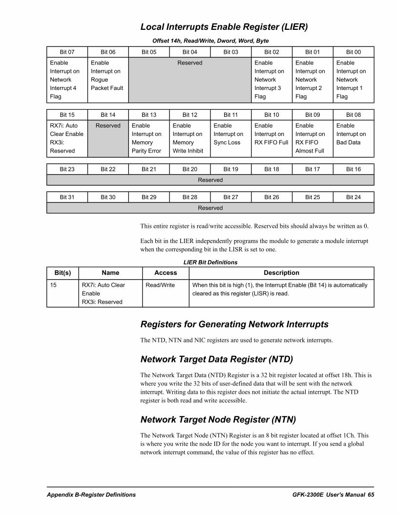
Local Interrupts Enable Register (LIER)Offset 14h, Read/Write, Dword, Word, Byte
Bit 07 Bit 06 Bit 05 Bit 04 Bit 03 Bit 02 Bit 01 Bit 00
EnableInterrupt onNetworkInterrupt 4Flag
EnableInterrupt onRoguePacket Fault
Reserved EnableInterrupt onNetworkInterrupt 3Flag
EnableInterrupt onNetworkInterrupt 2Flag
EnableInterrupt onNetworkInterrupt 1Flag
Bit 15 Bit 14 Bit 13 Bit 12 Bit 11 Bit 10 Bit 09 Bit 08
RX7i: AutoClear EnableRX3i:Reserved
Reserved EnableInterrupt onMemoryParity Error
EnableInterrupt onMemoryWrite Inhibit
EnableInterrupt onSync Loss
EnableInterrupt onRX FIFO Full
EnableInterrupt onRX FIFOAlmost Full
EnableInterrupt onBad Data
Bit 23 Bit 22 Bit 21 Bit 20 Bit 19 Bit 18 Bit 17 Bit 16
Reserved
Bit 31 Bit 30 Bit 29 Bit 28 Bit 27 Bit 26 Bit 25 Bit 24
Reserved
This entire register is read/write accessible. Reserved bits should always be written as 0.
Each bit in the LIER independently programs the module to generate a module interruptwhen the corresponding bit in the LISR is set to one.
LIER Bit Definitions
Bit(s) Name Access Description
15 RX7i: Auto ClearEnableRX3i: Reserved
Read/Write When this bit is high (1), the Interrupt Enable (Bit 14) is automaticallycleared as this register (LISR) is read.
Registers for Generating Network InterruptsThe NTD, NTN and NIC registers are used to generate network interrupts.
Network Target Data Register (NTD)The Network Target Data (NTD) Register is a 32 bit register located at offset 18h. This iswhere you write the 32 bits of user-defined data that will be sent with the networkinterrupt. Writing data to this register does not initiate the actual interrupt. The NTDregister is both read and write accessible.
Network Target Node Register (NTN)The Network Target Node (NTN) Register is an 8 bit register located at offset 1Ch. Thisis where you write the node ID for the node you want to interrupt. If you send a globalnetwork interrupt command, the value of this register has no effect.
Appendix B-Register Definitions GFK-2300E User's Manual 65

Writing to the NTN register does not initiate the actual network interrupt. This register isboth read and write accessible. The NTN register may be written or read together with theNetwork Interrupt Command Register (NIC) as a single BUS_WRT_WORD function.
Network Interrupt Command Register (NIC)Offset 1Dh, Read/Write, Dword, Word or Byte
The Network Interrupt Command (NIC) Register is an 8 bit register located at offset 1Dh.This is where you select the type of network interrupt you want to send. To determinewhich value to write, consult the table below. The NIC register is read and writeaccessible. Writing to the NIC register initiates the network interrupt.
Value Function00h Reserved. Do not use.
01h Send Network Interrupt type 1 to the node specified in the NTN register
02h Send Network Interrupt type 2 to the node specified in the NTN register
03h Send Network Interrupt type3 to the node specified in the NTN register
04h, 05h Reserved. Do not use.
06h Send a test interrupt packet around the ring. If this packet returns to theoriginator, the OWN DATA bit in the LCSR is set. The other nodes in thering are not affected. If you use this command, set the NTN to the nodeof the originator and set the NTD to FFFFFFFFh.
07h Send Network Interrupt type 4 to the node specified in the NTN register
08h Reserved. Do not use.
09h Send Network Interrupt type 1 to all other nodes on the network (global)
0Ah Send Network Interrupt type 2 to all other nodes on the network (global)
0Bh Send Network Interrupt type3 to all other nodes on the network (global)
0Ch–0Eh Reserved. Do not use.
0Fh Send Network Interrupt type 4 to all other nodes on the network (global).
10h-FF Reserved. Do not use.
Registers for Receiving Network InterruptsThe four pairs of registers, SID[4—1] and ISD[4—1], are used to retrieve networkinterrupts that have been received.
Interrupt Sender Data RegisterEach time a node issues a network interrupt, it includes its own node ID as part of thepacket. When the Memory Xchange module receives a network interrupt, it stores thesender’s node ID and the 32 bits of user defined data in the FIFO (first in first out) queueassociated with the Type of the network interrupt.
66 GFK-2300E PACSystems Memory Xchange Modules
Application logic may retrieve the 32 bits of user-defined data corresponding to the oldestentry in the FIFO by reading the Interrupt Sender Data (ISDx) register. Reading an ISDxregister does not remove the entry from the FIFO. Entries are only removed from theFIFO by accessing the Interrupt Sender Node ID register. Do not write to the ISDxregisters.
To determine if an entry is pending in the FIFO, examine the corresponding bit in theLISR.
Interrupt Sender Node ID RegistersEach time a node issues a network interrupt, it includes its own node ID as part of thepacket. When the Memory Xchange module receives a network interrupt, it stores thesender’s node ID and the 32 bits of user defined data in the FIFO associated with the Typeof the network interrupt.
Queue depth, or the number of interrupts each FIFO can store, is as follows:
RX7i CMX and RMX modules: 127 interrupts
RX3i CMX and RMX modules: 130 interrupts
Application logic may retrieve the Node ID of the oldest entry in the FIFO by reading theInterrupt Sender Node ID (SIDx) register. When this register is read, the entire entry(Node ID and user data) is removed from the FIFO. Therefore, each sender ID can onlybe read once. If the sender data is desired, read the corresponding Interrupt Sender Data(ISDx) register before reading the Interrupt Sender Node ID register.
To determine if an entry is pending in the FIFO, examine the corresponding bit in theLISR.
The SIDx registers are both read and write accessible. Writing any value to an SIDxregister empties the FIFO.
Interrupt 1 Sender Data (ISD1)Offset 20h, DWORD
Used to retrieve the 32 bits of user defined data for network interrupt type 1 as describedabove.
Interrupt 1 Sender Node ID (SID1)Offset 24h, BYTE
Used to read the sender’s Node ID for network interrupt type 1 and remove the entry fromthe FIFO as described above.
Interrupt 2 Sender Data (ISD2)Offset 28h, DWORD
Used to retrieve the 32 bits of user defined data for network interrupt type 2 as describedabove.
Appendix B-Register Definitions GFK-2300E User's Manual 67

Interrupt 2 Sender ID (SID2)Offset 2Ch, BYTE
Used to read the sender’s Node ID for network interrupt type 2 and remove the entry fromthe FIFO as described above.
Interrupt 3 Sender Data (ISD3)Offset 30h, DWORD
Used to retrieve the 32 bits of user defined data for network interrupt type 3 as describedabove.
Interrupt 3 Sender ID (SID3)Offset 34h, BYTE
Used to read the sender’s Node ID for network interrupt type 3 and remove the entry fromthe FIFO as described above.
Interrupt 4 Sender Data (ISD4)Offset 38h, DWORD
Used to retrieve the 32 bits of user defined data for network interrupt type 4 as describedabove.
Interrupt 4 Sender ID (SID4)Offset 3Ch, BYTE
Used to read the sender’s Node ID for network interrupt type 4 and remove the entry fromthe FIFO as described above.
68 GFK-2300E PACSystems Memory Xchange Modules
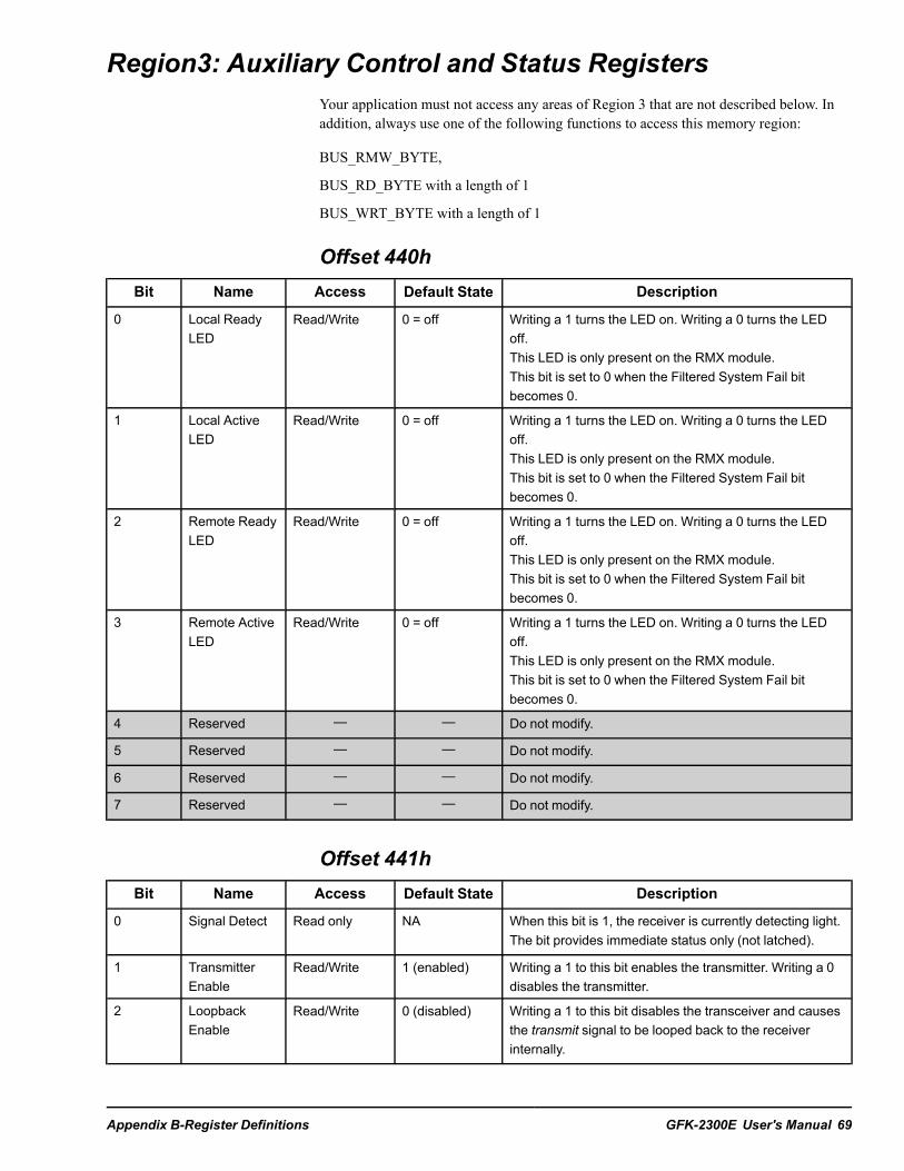
Region3: Auxiliary Control and Status RegistersYour application must not access any areas of Region 3 that are not described below. Inaddition, always use one of the following functions to access this memory region:
BUS_RMW_BYTE,
BUS_RD_BYTE with a length of 1
BUS_WRT_BYTE with a length of 1
Offset 440hBit Name Access Default State Description
0 Local ReadyLED
Read/Write 0 = off Writing a 1 turns the LED on. Writing a 0 turns the LEDoff.This LED is only present on the RMX module.This bit is set to 0 when the Filtered System Fail bitbecomes 0.
1 Local ActiveLED
Read/Write 0 = off Writing a 1 turns the LED on. Writing a 0 turns the LEDoff.This LED is only present on the RMX module.This bit is set to 0 when the Filtered System Fail bitbecomes 0.
2 Remote ReadyLED
Read/Write 0 = off Writing a 1 turns the LED on. Writing a 0 turns the LEDoff.This LED is only present on the RMX module.This bit is set to 0 when the Filtered System Fail bitbecomes 0.
3 Remote ActiveLED
Read/Write 0 = off Writing a 1 turns the LED on. Writing a 0 turns the LEDoff.This LED is only present on the RMX module.This bit is set to 0 when the Filtered System Fail bitbecomes 0.
4 Reserved — — Do not modify.
5 Reserved — — Do not modify.
6 Reserved — — Do not modify.
7 Reserved — — Do not modify.
Offset 441hBit Name Access Default State Description
0 Signal Detect Read only NA When this bit is 1, the receiver is currently detecting light.The bit provides immediate status only (not latched).
1 TransmitterEnable
Read/Write 1 (enabled) Writing a 1 to this bit enables the transmitter. Writing a 0disables the transmitter.
2 LoopbackEnable
Read/Write 0 (disabled) Writing a 1 to this bit disables the transceiver and causesthe transmit signal to be looped back to the receiverinternally.
Appendix B-Register Definitions GFK-2300E User's Manual 69

Bit Name Access Default State Description
3 Dark-on-DarkEnable
Read/Write 0 (disabled) Controls whether Dark-on-Dark is enabled (1), or not (0).If Dark-on-Dark is enabled, the module automaticallyturns off its transmitter whenever the Signal Detect bit is0. Also, when the Signal Detect bit becomes 1, thetransmitter is automatically turned on.Enabling Dark-on-Dark before Signal Detect becomes 1the first time is not recommended.
4 Auto TransmitDisable
Read/Write 0 (no Autodisable)
When this bit is 1, the transmitter is automaticallydisabled when the Filtered System Fail bit becomes 0.
5 CMX/RMXindicator
Read Only NA When this bit is 1, the module is an RMX. When this bit is0, the module is a CMX.
6 Reserved — 0 Do not modify.
7 Reserved — 0 Do not modify.
Offset 442hBit Name Access Default State Description
0 Reserved — 0 Do not modify.
1 Reserved — 0 Do not modify.
2 Clear Memory Read/Write 0 Write 1 to this bit to set all memory in Region 1 to zero.Once all memory has been cleared, this bit will be set to0.
3–7 Reserved — 0 Do not modify.
Offset 445hName Access Default State Description
Role Switch FilterTime
Read/Write 64h (1 sec.) Represents the filter time for the for the role switch input. Therole switch must be activated for this amount of time before theFiltered Role Switch State bit will be set to 1. Each countrepresents 0.01 seconds. Range is 0.01 seconds to 2.54seconds.This switch is present only on the RMX module.
70 GFK-2300E PACSystems Memory Xchange Modules

Offset 446hBit Name Access Default State Description
0 RX7i: FilteredSystem FailRX3i:Reserved
Read Only 1 RX7i: A 0 indicates that the CPU has failed. When set to0, all four Redundancy Status LEDs are turned off. Also,refer to the Auto Transmit Disable bit (bit 4), described inthe table in the section Offset 441h.RX3i and RX7i: Do not modify.
1 Current RoleSwitch State
Read Only NA Reflects the current state of the Role Switch input.The switch is only present in the RMX module.
2 Filtered RoleSwitch State
Read/Write 0 When this bit is 1, the Role Switch was held in the ONposition for the Role Switch Filter time or longer. This bitis latched. Write a 1 to clear this bit. Writing 0 has noeffect.
3–7 Reserved — 0 Do not modify.
Region 4: Interrupt Acknowledge RegisterYour application must not access any areas of Region 4 that are not described below.
Interrupt Acknowledge Register (IAKR)Offset: 68h, BYTE, WORD
Use of this register is demonstrated in chapter 5. Always use a BUS_RMWoperation toaccess this register.
Bit(s) Name Access Description
0–4 Reserved — Do not modify.
5 Reserved — Always write as zero (0)
6 Reserved — Do not modify.
7 RX7i: IAKRParity ErrorLatchRX3i: Reserved
Read/Write When set to 1, a parity error has been detected. Write a 1 to this bit to clearit. Always clear this bit before clearing bit 13 of the LISR.
8 Master InterruptEnable
Read/Write Write a 0 to this bit to acknowledge a module interrupt. Write a 1 to enablegeneration of a subsequent interrupt by the module.
9–15 Reserved — Do not modify.
Appendix B-Register Definitions GFK-2300E User's Manual 71

Appendix C-Reflective Memory ModuleStatus BitsIC695CMX128, IC695RMX128, and IC695RMX228
In PACSystems Release 8.15 or later Module Status Bits are available for theIC695CMX128, IC695RMX128, and IC695RMX228 modules. These Module Status bitscan be read using the BUS_READ_WORD function. If the function is successful, each bitreturned will reflect the current state of the corresponding bit on the module faceplate,with a value of 0 being the equivalent of the LED being OFF, and a value of 1 being theequivalent of the LED being ON. This request will only work for reflective memorymodules that are present and configured.
Instructions for UsageTo read this data use a BUS_READ_WORD function block:
LENGTH = 1
INPUTS:
Rack = 0
Slot = <actualSlot>
Subslot = 0
Region = 5
Offset = 0
OUTPUTS:
Status = BUS_RD_WORD execution status
Q = Module status
If the ST output is 0, the data returned on the Q output of the BUS_READ_WORD blockhas the following format:
Bit 07 Bit 06 Bit 05 Bit 04 Bit 03 Bit 02 Bit 01 Bit 00
Reserved OWNDATA
SIGDE-TECT
LINKOK /CONFIG
OK
Bit 15 Bit 14 Bit 13 Bit 12 Bit 11 Bit 10 Bit 09 Bit 08
Reserved
72 GFK-2300E PACSystems Memory Xchange Modules

Appendix C-Reflective Memory Module Status Bits GFK-2300E User's Manual 73

Notes
74 GFK-2300E PACSystems Memory Xchange Modules