Optomechanical and photothermal interactions in suspended photonic
18
Optomechanical and photothermal interactions in suspended photonic crystal membranes David Woolf, 1 Pui-Chuen Hui, 1 Eiji Iwase, 1,3 Mughees Khan, 1,4 Alejandro W. Rodriguez, 1,2 Parag Deotare, 1,5 Irfan Bulu, 1 Steven G. Johnson, 2 Federico Capasso, 1 and Marko Loncar 1∗ 1 School of Engineering and Applied Sciences, Harvard University, Cambridge, MA 02138 USA 2 Department of Mathematics, Massachusetts Institute of Technology, Cambridge, MA 02139 USA 3 Department of Applied Mechanics and Aerospace Engineering, Waseda University, Tokyo, 169-8555, Japan 4 Wyss Institute, Harvard University, Boston, MA 02115 USA 5 Department of Electrical Engineering, Massachusetts Institute of Technology, Cambridge, MA 02139 USA ∗ loncar@seas harvard.edu Abstract: We present here an optomechanical system fabricated with novel stress management techniques that allow us to suspend an ultrathin defect-free silicon photonic-crystal membrane above a Silicon-on-Insulator (SOI) substrate with a gap that is tunable to below 200 nm. Our devices are able to generate strong attractive and repulsive optical forces over a large surface area with simple in- and out- coupling and feature the strongest repulsive optomechanical coupling in any geometry to date (g OM /2π ≈ -65 GHz/nm). The interplay between the optomechanical and photo-thermal- mechanical dynamics is explored, and the latter is used to achieve cooling and amplification of the mechanical mode, demonstrating that our platform is well-suited for potential applications in low-power mass, force, and refractive-index sensing as well as optomechanical accelerometry. © 2013 Optical Society of America OCIS codes: (120.4880) Optomechanics; (230.5298) Photonic crystals; (230.4000) Mi- crostructure fabrication. References and links 1. N. V. Lavrik and P. G. Datskos, “Femtogram mass detection using photothermally actuated nanomechanical resonators,” Appl. Phys. Lett. 82, 2697–2699 (2003). 2. X. L. Feng, C. J. White, A. Hajimiri, and M. L. Roukes, “A self-sustaining ultrahigh-frequency nanoelectrome- chanical oscillator,” Nat. Nanotechnol. 3, 342–346 (2008). 3. B. R. Ilic, S. Krylov, M. Kondratovich, and H. G. Craighead, “Optically actuated nanoelectromechanical oscilla- tors,” IEEE J. Sel. Top. Quantum Electron. 13, 392–399 (2007). 4. Y. T. Yang, Y. T., Callegari, C., Feng, X. L., Ekinci, K. L., and Roukes, M. L., “Zeptogram-scale nanomechanical mass sensing,” Nano Lett. 6, 583–586 (2006). 5. M. Eichenfield, R. Camacho, J. Chan, K. J. Vahala, and O. Painter, “A picogram- and nanometre-scale photonic- crystal optomechanical cavity,” Nature 459, 550–579 (2009). 6. C. H. Metzger and K. Karrai, “Cavity cooling of a microlever,” Nature 432, 1002–1005 (2004). 7. T. J. Kippenberg and K. J. Vahala, “Cavity opto-mechanics,” Opt. Express 15, 17172–17205 (2007). 8. A. Schliesser, P. Del’Haye, N. Nooshi, K. J. Vahala, and T. J. Kippenberg, “Radiation pressure cooling of a micromechanical oscillator using dynamical backaction,” Phys. Rev. Lett. 97, 243905 (2006). #181620 - $15.00 USD Received 12 Dec 2012; revised 25 Feb 2013; accepted 26 Feb 2013; published 15 Mar 2013 (C) 2013 OSA 25 March 2013 / Vol. 21, No. 6 / OPTICS EXPRESS 7258
Transcript of Optomechanical and photothermal interactions in suspended photonic

Optomechanical and photothermalinteractions in suspended photonic
crystal membranes
David Woolf,1 Pui-Chuen Hui,1 Eiji Iwase,1,3 Mughees Khan,1,4
Alejandro W. Rodriguez,1,2 Parag Deotare,1,5 Irfan Bulu,1 Steven G.Johnson,2 Federico Capasso,1 and Marko Loncar1∗
1School of Engineering and Applied Sciences, Harvard University, Cambridge, MA 02138USA
2Department of Mathematics, Massachusetts Institute of Technology, Cambridge, MA 02139USA
3Department of Applied Mechanics and Aerospace Engineering, Waseda University, Tokyo,169-8555, Japan
4Wyss Institute, Harvard University, Boston, MA 02115 USA5Department of Electrical Engineering, Massachusetts Institute of Technology, Cambridge,
MA 02139 USA∗loncar@seas harvard.edu
Abstract: We present here an optomechanical system fabricated withnovel stress management techniques that allow us to suspend an ultrathindefect-free silicon photonic-crystal membrane above a Silicon-on-Insulator(SOI) substrate with a gap that is tunable to below 200 nm. Our devices areable to generate strong attractive and repulsive optical forces over a largesurface area with simple in- and out- coupling and feature the strongestrepulsive optomechanical coupling in any geometry to date (gOM/2π ≈ -65GHz/nm). The interplay between the optomechanical and photo-thermal-mechanical dynamics is explored, and the latter is used to achieve coolingand amplification of the mechanical mode, demonstrating that our platformis well-suited for potential applications in low-power mass, force, andrefractive-index sensing as well as optomechanical accelerometry.
© 2013 Optical Society of America
OCIS codes: (120.4880) Optomechanics; (230.5298) Photonic crystals; (230.4000) Mi-crostructure fabrication.
References and links1. N. V. Lavrik and P. G. Datskos, “Femtogram mass detection using photothermally actuated nanomechanical
resonators,” Appl. Phys. Lett. 82, 2697–2699 (2003).2. X. L. Feng, C. J. White, A. Hajimiri, and M. L. Roukes, “A self-sustaining ultrahigh-frequency nanoelectrome-
chanical oscillator,” Nat. Nanotechnol. 3, 342–346 (2008).3. B. R. Ilic, S. Krylov, M. Kondratovich, and H. G. Craighead, “Optically actuated nanoelectromechanical oscilla-
tors,” IEEE J. Sel. Top. Quantum Electron. 13, 392–399 (2007).4. Y. T. Yang, Y. T., Callegari, C., Feng, X. L., Ekinci, K. L., and Roukes, M. L., “Zeptogram-scale nanomechanical
mass sensing,” Nano Lett. 6, 583–586 (2006).5. M. Eichenfield, R. Camacho, J. Chan, K. J. Vahala, and O. Painter, “A picogram- and nanometre-scale photonic-
crystal optomechanical cavity,” Nature 459, 550–579 (2009).6. C. H. Metzger and K. Karrai, “Cavity cooling of a microlever,” Nature 432, 1002–1005 (2004).7. T. J. Kippenberg and K. J. Vahala, “Cavity opto-mechanics,” Opt. Express 15, 17172–17205 (2007).8. A. Schliesser, P. Del’Haye, N. Nooshi, K. J. Vahala, and T. J. Kippenberg, “Radiation pressure cooling of a
micromechanical oscillator using dynamical backaction,” Phys. Rev. Lett. 97, 243905 (2006).
#181620 - $15.00 USD Received 12 Dec 2012; revised 25 Feb 2013; accepted 26 Feb 2013; published 15 Mar 2013(C) 2013 OSA 25 March 2013 / Vol. 21, No. 6 / OPTICS EXPRESS 7258

9. C. Genes, D. Vitali, P. Tombesi, S. Gigan, and M. Aspelmeyer, “Ground-state cooling of a micromechanicaloscillator: Comparing cold damping and cavity-assisted cooling schemes,” Phys. Rev. A 79, 033804 (2009).
10. R. Riviere, S. Deleglise, S. Weis, E. Gavartin, O. Arcizet, A. Schliesser, and T. J. Kippenberg, “Optomechanicalsideband cooling of a micromechanical oscillator close to the Quantum ground state,” Phys. Rev. A 83, 063835(2011).
11. J. Chan, T. P. M. Alegre, A. H. Safavi-Naeini, J. T. Hill, A. Krause, S. Groblacher, M. Aspelmeyer, and O. Painter,“Laser cooling of a nanomechanical oscillator into its quantum ground state,” Nature 478, 89–92 (2011).
12. M. Eichenfield, J. Chan, R. M. Camacho, K. J. Vahala, and O. Painter, “Optomechanical crystals,” Nature 462,78–82 (2009).
13. A. Krause, M. Winger, T. D. Blasius, Q. Lin, and O. Painter, ”A high-resolution microchip optomechanicalaccelerometer,” Nat Photonics 6, 768–772 (2012).
14. O. Arcizet, P.F. Cohadon, T. Briant, M. Pinard, and A. Heidmann, “Radiation-pressure cooling and optomechan-ical instability of a micromirror,” Nature 444, 71–74 (2006).
15. M. W. Pruessner, T. H. Stievater, J. B. Khurgin, and W. S. Rabinovich, “Integrated waveguide-DBR microcavityopto-mechanical system,” Opt. Express 19, 21904–21918 (2011).
16. H. Fu, C. D. Liu, Y. Liu, J. R. Chu, and G. Y. Cao, “Selective photothermal self-excitation of mechanical modesof a micro-cantilever for force microscopy,” Appl. Phys. Lett. 99, 173501 (2011).
17. Q. Lin, J. Rosenberg, X. S. Jiang, K. J. Vahala, and O. Painter, “Mechanical oscillation and cooling actuated bythe optical gradient force,” Phys. Rev. Lett. 103, 103601 (2009).
18. G. Anetsberger, O. Arcizet, Q. P. Unterreithmeier, R. Riviere, A. Schliesser, E. M. Weig, J. P. Kotthaus, and T. J.Kippenberg, “Near-field cavity optomechanics with nanomechanical oscillators,” Nat. Phys. 5, 909–914 (2009).
19. M. Li, M., W. H. P. Pernice, and H. X. Tang, “Reactive cavity optical force on microdisk-coupled nanomechanicalbeam waveguides,” Phys. Rev. Lett. 103, 223901 (2009).
20. G. S. Wiederhecker, L. Chen, A. Gondarenko, and M. Lipson, “Controlling photonic structures using opticalforces,” Nature 462, 633–636 (2009).
21. M. Li, W. H. P. Pernice, C. Xiong, T. Baehr-Jones, M. Hochberg, and H. X. Tang, “Harnessing optical forces inintegrated photonic circuits,” Nature 456, 480–484 (2008).
22. M. L. Povinelli, S. G. Johnson, M. Loncar, M. Ibanescu, E. J. Smythe, F. Capasso, and J. D. Joannopoulos, “High-Q enhancement of attractive and repulsive optical forces between coupled whispering-gallery-mode resonators,”Opt. Express 13, 8286–8295 (2005).
23. M. L. Povinelli, M. Loncar, M. Ibanescu, E. J. Smythe, S. G. Johnson, F. Capasso, and J. D. Joannopoulos,“Evanescent-wave bonding between optical waveguides,” Opt. Lett. 30, 3042–3044 (2005).
24. M. Li, W. H. P. Pernice, and H. X. Tang, “Tunable bipolar optical interactions between guided lightwaves,” Nat.Photonics 3, 464–468 (2009).
25. The expresion for the force is only strictly true when the (complex) wavevector is constant under translation,though it can still be used when the change in optical Q is small over the distance ds.
26. A. W. Rodriguez, F. Capasso, and S. G. Johnson, “Bonding, antibonding and tunable optical forces in asymmetricmembranes,” Opt. Express 19, 2225–2241 (2011).
27. J. Lee, B. Zhen, S. L. Chua, W. J. Qiu, J. D. Joannopoulos, M. Soljacic, and O. Shapira, “Observation anddifferentiation of unique high-Q optical resonances near zero wave Vector in macroscopic photonic crystal slabs,”Phys. Rev. Lett. 109, 067401 (2012).
28. E. Iwase, P. C. Hui, D. Woolf, A. W. Rodriguez, S. G. Johnson, F. Capasso, and M. Loncar, “Control of bucklingin large micromembranes using engineered support structures” J. Micromech. Microeng. 22, 065028 (2012).
29. D. Blocher, A. T. Zehnder, R. H. Rand, and S. Mukerji, “Anchor deformations drive limit cycle oscillations ininterferometrically transduced MEMS beams,” Finite. Elem. Anal. Des. 49, 52–57 (2012).
30. P. B. Deotare, I. Bulu, I. W. Frank, Q. M. Quan, Y. N. Zhang, R. Ilic, and M. Loncar, “All optical reconfigurationof optomechanical filters” Nat Commun 3, 846 (2012).
31. Y. Y. Gong, A. Rundquist, A. Majumdar, and J. Vuckovic, “Low power resonant optical excitation of an optome-chanical cavity,” Opt. Express 19, 1429–1440 (2011).
32. T. J. Johnson, M. Borselli, and O. Painter, “Self-induced optical modulation of the transmission through a high-Qsilicon microdisk resonator,” Opt. Express 14, 817–831 (2006).
33. S. H. Fan, and J. D. Joannopoulos, “Analysis of guided resonances in photonic crystal slabs,” Phys. Rev. B 65,235112 (2002).
34. Near-field thermal heat-transfer will modify γt by a small amount, though we ignore this small effect in ouranalysis here for simplicity.
35. H.A. Haus, Waves and Fields in Optoelectronics (Prentice-Hall, 1984).36. D. Rugar, H. J. Mamin, and P. Guethner, “Improved Fiber-Optic Interferometer for Atomic Force Microscopy,”
Appl. Phys. Lett. 55, 2588–2590 (1989).37. E. R. I. Abraham, and E. A. Cornell, ”Teflon feedthrough for coupling optical fibers into ultrahigh vacuum
systems,” Appl. Optics 37, 1762–1763 (1998).38. K. J. Vahala, “Back-action limit of linewidth in an optomechanical oscillator,” Phys Rev A 78, 023832 (2008).39. J. O. Grepstad, P. Kaspar, O. Solgaard, I. R. Johansen, and A. S. Sudbo, “Photonic-crystal membranes for optical
#181620 - $15.00 USD Received 12 Dec 2012; revised 25 Feb 2013; accepted 26 Feb 2013; published 15 Mar 2013(C) 2013 OSA 25 March 2013 / Vol. 21, No. 6 / OPTICS EXPRESS 7259

detection of single nano-particles, designed for biosensor application,” Opt. Express 20, 7954–7965 (2012).40. M. El Beheiry, V. Liu, S. H. Fan, and O. Levi, “Sensitivity enhancement in photonic crystal slab biosensors,”
Opt. Express 18, 22702–22714 (2010).41. T. P. Burg, A. R. Mirza, N. Milovic, C. H. Tsau, G. A. Popescu, J. S. Foster, and S. R. Manalis, ”Vacuum-
packaged suspended microchannel resonant mass sensor for biomolecular detection,” J. Microelectromech S 15,1466–1476 (2006).
42. P. S. Waggoner, and H. G. Craighead, “Micro- and nanomechanical sensors for environmental, chemical, andbiological detection,” Lab Chip 7, 1238–1255 (2007).
43. J. L. Arlett, E. B. Myers, and M. L. Roukes, “Comparative advantages of mechanical biosensors,” Nat. Nanotech-nol 6, 203–215 (2011).
44. H. B. Chan, V. A. Aksyuk, R. N. Kleiman, D. J. Bishop, and F. Capasso, “Nonlinear micromechanical Casimiroscillator,” Phys. Rev. Lett. 87, 211801 (2001).
45. H. B. Chan, V. A. Aksyuk, R. N. Kleiman, D. J. Bishop, and F. Capasso,“Quantum mechanical actuation ofmicroelectromechanical systems by the Casimir force,” Science 293, 607–607 (2001).
46. A. W. Rodriguez, F. Capasso, and S. G. Johnson, “ The Casimir effect in microstructured geometries,” Nat.Photonics 5, 211–221 (2011).
47. S. J. Rahi, A. W. Rodriguez, T. Emig, R. L. Jaffe, S. G. Johnson, and M. Kardar, “Nonmonotonic effects ofparallel sidewalls on Casimir forces between cylinders,” Phys. Rev. A 77, 030101 (2008).
48. J. L. Yang, T. Ono, and M. Esashi, “Surface effects and high quality factors in ultrathin single-crystal siliconcantilevers,” Appl. Phys. Lett. 77, 3860–3862 (2000).
49. M. Borselli, T. J. Johnson, and O. Painter, “ Measuring the role of surface chemistry in silicon microphotonics,”Appl. Phys. Lett. 88, 131114 (2006).
1. Introduction
Devices exhibiting resonant mechanical dynamics have applications ranging from high-precision mass and force sensing in nanoelectromechanical systems (NEMS) [1–5] to novelquantum manipulation enabled by ground-state cooling of sub-micron-scale mechanical ob-jects [6–11]. Additionally, the concentration of light into small volumes has been shown tohave broad applications due to the sensitivity of the optical mode properties to its local envi-ronment [12, 13]. Recently, there have been rapid developments in the field of optomechanicsthat utilize light to actuate a new class of low-mass compact resonators [3,13–16] and that pushthe limits of device scalability [1, 5, 17–19]. In particular, optomechanical devices that can befully integrated onto a silicon chip can act as active sensors or reconfigurable elements in chip-based systems [15, 19–21]. Here, we present a versatile optomechanical structure fabricatedwith novel stress management techniques that allow us to suspend an ultrathin defect-free sili-con photonic-crystal membrane above a Silicon-on-Insulator (SOI) substrate with a gap that istunable to below 200 nm. Our devices are able to generate strong attractive and repulsive opticalforces over a large surface area and feature the strongest repulsive optomechanical coupling inany geometry to date (gOM/2π ≈ -65 GHz/nm). The interplay between the optomechanical andphoto-thermal-mechanical dynamics is explored, and the latter is used to achieve cooling ofthe mechanical mode from room temperature down to 5 K with approximately one milliwatt ofpower and amplification of the mode to achieve three orders of magnitude of linewidth narrow-ing and oscillation amplitudes of approximately 1 nm. We achieve these figures by leveraging adelocalized “dark” mode of our optical system that minimize the impact of two-photon absorp-tion while simultaneously generating large forces in our devices. Owing to the simplicity of thein- and out-coupling of light as well as its large surface area, our platform is well-suited forpotential applications in both mass sensing and refractive index sensing and optomechanicalaccelerometry.
It has been previously shown [22–24] that two co-propagating modes at optical frequencyω in parallel dielectric waveguides separated by a distance sinteract evanescently, resulting in“bonding” and “antibonding” eigenmodes of the structure. As s decreases, the coupling be-tween the two waveguides increases, decreasing the eigenfrequency of the bonding mode andincreasing the eigenfrequency of the antibonding mode. The force between the two waveguides
#181620 - $15.00 USD Received 12 Dec 2012; revised 25 Feb 2013; accepted 26 Feb 2013; published 15 Mar 2013(C) 2013 OSA 25 March 2013 / Vol. 21, No. 6 / OPTICS EXPRESS 7260

can be written as
Fopt =UphgOM
ω, (1)
where Uph= N�ω is the energy flowing in the waveguides, N is the number of photons inthe mode, and gOM is the optomechanical (OM) coupling coefficient, defined as dω/ds. Inthe “bonding” configuration, the fields in the two waveguides are in-phase and generate anattractive force (dω/ds > 0), while the “antibonding” configuration corresponds to out-of-phasefields and a repulsive (dω/ds < 0) interaction.
2. Fabrication and characterization
Because Eq. (1) is general [25], we can extend it beyond the parallel waveguide geometry andapply it to our platform, shown in Fig. 1(a).The platform consists of a square silicon photoniccrystal (PhC) slab containing a 30 × 30 array of holes with periodicity p = 0.92μm and holediameter d = 0.414μm, as defined in the illustration in Fig. 1(b), suspended a few hundrednanometers above a Silicon-on-Insulator (SOI) substrate and is capable of generating strongattractive and repulsive forces [26]. To fabricate our devices, we oxidize the top 35 nm of twoSOI wafers (device layer thickness = 220 nm, buried oxide layer thickness = 2 μm) and bond thetwo oxidized surfaces together. After removal of one of the handle wafers along with its buriedoxide layer, we are left with a double-device layer SOI with two thin silicon layers of thicknessh = 185 nm separated by a thin oxide layer of thickness s0 = 260 nm. Using e-beam lithography,we write our device pattern into a thin layer of electron-beam resist, which then acts as a maskas we etch through the top silicon layer using Reactive Ion Etching. The top membrane isthen released by removing the thin oxide layer with Hydrogen Fluoride Vapor-phase Etching(HFVE) (see Appendix B for details). The device parameters p and d were chosen to result inan antibonding mode (profile shown in Fig. 1(c)) in the wavelength range accessible by ourlasers (1480-1680 nm). We note that the field symmetry indicates that this is a dark mode of thestructure and thus should not couple directly to free space. However, due to the finite size of ourmembrane, we are able to break the structural symmetry to access the mode [27]. The opticalresonance frequency can be tuned by controlling the membrane-substrate separation s (red linein Fig. 1(d). Using numerical modeling performed in COMSOL Multiphysics, we find that thegOM (blue line, Fig. 1(d)) of the mode is 2π × -3.3 GHz/nm at s = 350 nm and increases to 2π× -150 GHz/nm at s = 50 nm.
We explore this range of separations using novel techniques that we developed to leveragebuilt-in stresses in the substrate. Commercial SOI wafers often have high levels of built in stressintroduced during the process that bonds the device layer and buried oxide layer to the handlesubstrate [28], but the sign and precise strength of the stress are often unknown. Furthermore,devices made in our double-SOI platform experience an additional bending moment tangentialto the SiO2 surfaces exposed during the HFVE process that produces an upward force on all un-dercut structures (see Appendix B). To control these effects, we first introduce “accordion-like”arrays of narrow beams (Fig. 1(a) inset) to each arm that relieve the compressive (tensile) stressand prevent out-of plane buckling (breaking) through in-plane deformation of the accordionstructure [28]. Next, we introduce shaped arrays of etch-holes at the base of each arm to mod-ify the direction of the bending moment and thus control the resulting force on the membranearms. Devices which do not contain either of these stress management techniques, such as theone pictured in Fig. 2(a), deflect upward by >350 nm, as shown in the optical profilometermeasurement in Fig. 2(b). Introduction of the accordion-like structure and a rectangle-like ar-ray of etch-holes decrease the membrane deflection by over an order of magnitude (Fig. 2(d,e)).Importantly, by replacing the rectangle-like etch-hole pattern with a triangular one, we are ableto deflect the membrane downward as seen in Fig. 2(g,h) by 105 nm. Measured deflections
#181620 - $15.00 USD Received 12 Dec 2012; revised 25 Feb 2013; accepted 26 Feb 2013; published 15 Mar 2013(C) 2013 OSA 25 March 2013 / Vol. 21, No. 6 / OPTICS EXPRESS 7261

Fig. 1. (a) SEM image of a device consisting of a h = 185 nm thick silicon membrane pat-terned with a square-lattice photonic crystal with a 30×30 periodic hole array of period p =0.92 μm and hole diameter d = 0.414 μm suspended 165 nm above a Silicon-on-Insulator(SOI) substrate (h = 185 nm, buried oxide layer = 2 μm, cross-section shown schematicallyin (b)). The membrane is supported by four arms (L = 19.3 μm, W = 2.75 μm) that are ter-minated on their far ends by arrays of etch holes and on their near ends by “accordion-like”structures (inset i) which provide lithographic control of membrane-substrate separation.(c) A 3D optical mode simulation shows the x-component of the electric field of a singleunit cell of the geometry in (b) with s = 100 nm for an antibonding mode of the struc-ture at λ 0=1570 nm. The antisymmetric field symmetry with respect to the gap betweenthe membrane and the substrate implies that this optical mode generates a repulsive force.(d) The calculated resonance wavelength λ 0 (red line) of the mode in (c) is plotted withdata points (red circles) representing 16 different devices with identical membrane designsbut different membrane-substrate separations. The separations were determined by inter-ferometric measurements using an optical profilometer. The blue line is optomechanicalcoupling coefficient of the mode and is proportional to the slope of the red line (gOM∝-dλ /ds).
(Fig. 2(b,d,h)) were consistent between identially-designed devices to within 20 nm. These ex-perimental observations were verified by numerical modeling of the devices under the samecompressive stress conditions performed in COMSOL Multiphysics (Fig. 2(c,f,i)).This is animportant and novel feature of our platform that gives us independent lithographic control ofthe membrane-substrate separation of different devices on the same chip. We have fabricateddevices (red circles, Fig. 1(d)) with separations as small as 135 nm, corresponding to a gOM
of -2π × 65 GHz/nm, which is the largest yet value of gOM seen in a repulsive system [20]by a factor of four. Finally, we note that our devices are designed such that the majority ofdevice deflection occurs in the support arms. Simulations show that the membrane has a radius
#181620 - $15.00 USD Received 12 Dec 2012; revised 25 Feb 2013; accepted 26 Feb 2013; published 15 Mar 2013(C) 2013 OSA 25 March 2013 / Vol. 21, No. 6 / OPTICS EXPRESS 7262

of curvature of 2 cm for 100 nm deflections, such that it remains essentially flat during ourexperiments. However, confocal measurements using an optical profilometer on fabricated de-vices indicate that anisotropy intrinsic to the HFVE process can induce tilts in our devices thatcan be as large as 10 nanometers from side to side. Further modifications to the device designand fabrication process should be able to minimize this tilt, making this system a good candi-date not only for current MEMS technologies but also for other innovative structures requiringparallel-plate geometries, such as plate-plate Casimir oscillators.
Fig. 2. Scanning Electron Microscope (SEM) images (a,d,g), optical profilometer imagesshowing interferometric measurements of height (b,c,h) and mechanical simulations inCOMSOL Multiphysics confirming the behavior measured by the profilometer (d,f,i) areshown for three separate devices. The first device (a) has simple support arms which offerno control over the stresses inherent in the wafer. The result is a membrane which deflectsstrongly upward by 365 nm (b,c) due to compressive stress in the membrane and an upwardtorque caused by a bending moment at the Si-SiO2 etch boundary. The second device (b)has an accordion-like structures between the arms and the membrane (see inset, Fig. 1(a))and an approximately rectangular etch-hole pattern at the base of each arm to combat com-pressive stress and the bending moment at the etch boundary. The result is a device whichonly deflects upward 35 nm (e,f), an order of magnitude improvement over the device in(a). The triangular design of the etch-hole pattern in the third device (g) utilizes the torqueinduced at the etch boundary to generate a controllable downward deflection. The result(h,i) is a membrane which deflects downward 105 nm from the surrounding silicon layer.
Actuation in our system is achieved by a combination of optical and photothermal forces, thelatter of which arises from absorption of light in the cavity that generates displacements throughthermal expansion at the Silicon-SiO2interface [6, 15, 16, 29]. Light absorption can also di-rectly change the optical properties of the mode by modifying the refractive index of the siliconthrough the thermal-optic effect (dn/dT). In previous studies, which featured wavelength-scalemode-volumes (≈ (λ 0/n)3) and poor thermal transport properties [30, 31], the thermo-opticeffect obscured the underlying optomechanics [32], due in large part to the strong two-photonabsorption in silicon at near-IR frequencies. By employing a system containing extended pho-
#181620 - $15.00 USD Received 12 Dec 2012; revised 25 Feb 2013; accepted 26 Feb 2013; published 15 Mar 2013(C) 2013 OSA 25 March 2013 / Vol. 21, No. 6 / OPTICS EXPRESS 7263

tonic crystal modes [26, 33] with large optical mode volumes (≈ 1500(λ0/m)3) and thermaldiffusion rates γ t (≈ 450 kHz) orders of magnitude larger than those of microcavity geome-tries, we avoid the problems commonly associated with silicon optomechanical systems whilestill achieving optical forces comparable to those achieved with micocavities.
To quantify the photo-thermal-mechanical (PtM) effects relative to the optomechanical (OM)
effects, we define coefficients LOM = ω0/gOM and LPtM =[DC−1
th Γabs]−1
(Ω2m + γ2
t )/γ t as theinverse of the optical and photo-thermal forces, respectively, per unit stored optical energy inthe cavity, where D is the material- and geometry-dependent thermal-mechanical force coef-ficient in units of Newtons per Kelvin (positive or negative for attractive or repulsive forces,respectively), Cthis the heat capacity, and Γabs is the total absorption coefficient of the mate-rial. In our devices, thermal expansion causes a downward deflection, effectively generating anattractive force (Fpth) between the membrane and the substrate, which puts the photo-thermalforce in competition with the repulsive optical force. We note that Fpth and LPtM are essentiallyindependent of membrane-substrate separation [34], while, as shown in Fig 1(c), Fopt and LOM
are highly sensitive to changes in s.Coupled-mode theory [35] is used to study how the coupling of the thermal, optical and
mechanical degrees of freedom affects a device’s mechanical angular frequency, Ωm and itslinewidth, Γm. (For full derivation, see Appendix A.) Physically, an optical cavity with linewidthκ in a free-standing membrane undergoing Brownian motion (with an RMS amplitude ds atΩm) is perturbed by the optical field or thermal gradient such that the resonant frequency shifts(ω ′
0 = ω0 +gOMδ s+ dωdT δT ), thus modulating the detuning Δ′
0 ≡ ωl −ω ′0 between an incident
laser source at ω l and the shifted cavity resonance. This modulation in Δ′0 further modulates the
stored cavity energy Uph, the forces Fopt and Fpth and hence the overall displacement, which inturn modulates the optical resonance frequency and forms a feedback loop. This feedback hasboth in-phase and quadrature (out-of-phase) components that result in a mechanical frequencyperturbation Ωm and a mechanical linewidth perturbation Γm, respectively, both of which haveodd symmetry with respect to Δ′
0.Modifications to Ωm can take two forms. The applied forces can act in the same direction of
the vibrational restoring force, resulting in a stiffening (δΩm > 0), or in the opposite direction,resulting in softening (δΩm< 0). Similarly, modifications to Γm, known as “induced back-action [7],” describe the direction of energy flow between the mechanical mode and the opticalor thermal field. A net energy flow into the mechanical mode decreases Γm and correspondsto mechanical amplification, while a net energy flow out of the mechanical mode increases Γm
and corresponds to increased damping (i.e. mechanical cooling). The strengths and signs of themodifications to the mechanical motion due to PtM and OM effects depend on the magnitudesof the respective forces (L−1
OM ,L−1PtM) as well as the strength of the optomechanical coupling, gOM .
This results in OM perturbations which are independent of the sign of the force (gOM/LOM)and PtM perturbations which depend on the signs of both the optical and photothermal forces(gOM/LPtM).
3. Results
To study these dynamics and characterize our devices, we use the setup illustrated in Fig. 3.Briefly, an optical fiber mounted on a z-translation stage centered above the suspended mem-brane in the Rugar configuration [36] (detail in inset i.) is used to couple light into a deviceand also collect the signal back-reflected by the device. The chip containing the device rests ona four-axis (x,y,θ x,θ y) stage platform. The motorized x-y stage contains closed-loop feedbackthat allows us to repeatably align the fiber to the sample with sub-100 nm resolution, while themanual θ x and θ y tilt stages are used to planarize the fiber facet to the chip surface. The wholesetup is placed inside a high vacuum chamber (10−5 torr) to eliminate gas damping of the me-
#181620 - $15.00 USD Received 12 Dec 2012; revised 25 Feb 2013; accepted 26 Feb 2013; published 15 Mar 2013(C) 2013 OSA 25 March 2013 / Vol. 21, No. 6 / OPTICS EXPRESS 7264

chanical vibrations. Optical spectra (Fig. 3, inset ii) were collected by sweeping the tunablelaser sources across the optical resonance. Mechanical spectra (Fig. 3, inset iii) were collectedat fixed excitation wavelengths on either side of the optical resonance by analyzing the sig-nal reflected off of our membranes in a real-time spectrum analyzer (Tektronix RSA3303B).Measurements were made after parallelizing the fiber facet to the substrate from fiber-substrateheights of approximately 25 μm (Fig. 3, inset i) corresponding to a spot size of approximately12 μm. This configuration allows straightforward coupling into the evanescently-coupled lat-eral modes of the PC membrane-substrate geometry at the Γpoint of the band structure. In allexperiments, we chose the fiber-membrane alignment which maximized coupling. We measurethe dynamic shifts in Ωm and Γm of the fundamental flexural mode of two different devices byfitting the measured mechanical resonance to a Lorentzian lineshape, and the best-fit parametersfor Ωm and Γm are plotted in Fig. 4 (green circles) as a function of laser wavelength.
Fig. 3. Experimental apparatus. The outputs from two tunable near IR lasers (λ = 1480nm-1580 nm and λ = 1580 nm-1680 nm) are combined using a fiber-directional coupler.Half of the signal is diverted to Photodetector 2 as a reference and half is coupled into ahigh –vacuum chamber (HVC) via a custom made fiber-feedthrough port [?]. The cleavedfiber is positioned above the center of the device, so that the cleaved fiber facet is parallelto the membrane (inset i., not to scale). The reflected optical signal is measured at Photode-tector 1. Optical reflection spectra are taken by sweeping the lasers’ wavelengths acrossthe optical resonances and collecting the signal via the Data Acquisition (DAQ) board. Theoptical resonance centered at λ 0 = 1561.1 nm (inset ii) has a Fano shape (black line) andQopt = 2500. Mechanical spectra are obtained by taking the Fourier transform of the pho-todetector signal using the spectrum analyzer (SA) to measure the small thermal vibrationsof the membrane. The fundamental mechanical resonance (inset iii), defined by resonancefrequency Ωm and linewidth Γm, is shown for a low-power measurement at λ=1561.2 nm(red dot, inset ii.).
We first explore an upward-deflected device (Fig. 1(d)) with membrane-substrate separation s= 300 nm at an incident optical power of 50 μW, in Fig 4(a). We observe blue-detuned (Δ′
0 > 0)cooling and softening and red-detuned (Δ′
0 < 0) amplification and stiffening, which fit well totheoretical predictions (black lines) for LOM = -95 μm (gOM = 2π × -3.3 GHz/nm) and LPtM =15 μm. As expected, PtM effects (red dashed lines) to dominate the dynamics due to the largemembrane-substrate separation. Furthermore, we see no OM contributions (blue-dashed line)
#181620 - $15.00 USD Received 12 Dec 2012; revised 25 Feb 2013; accepted 26 Feb 2013; published 15 Mar 2013(C) 2013 OSA 25 March 2013 / Vol. 21, No. 6 / OPTICS EXPRESS 7265

to the linewidth dynamics as a consequence of operating in the deep “sideband-unresolved”limit [7] where κ/Ωm > 106. In this regime, the optical force acting on the mechanical oscillatoris effectively instantaneous with respect to the oscillator period. All back-action in our devicesis provided by PtM effects.
Fig. 4. Optomechanical coupling curves for two devices with different membrane-substrateseparations experiencing photothermal and optical forces. Data (green circles) were col-lected by measuring the vibrational spectra (Fig. 3, inset iii.) for several wavelengths aroundthe cavity resonance. The data in (a) correspond to the device in Fig. 2(d), whose cavityresonance is centered at λ 0=1576.4 nm. The data in (b) correspond to the device in Fig.2(g), whose cavity resonance is centered at λ 0=1561.1nm. The photothermal force Fpth(red arrows, top insets) is attractive and approximately constant in both devices. The re-pulsive optical force Fopt (blue arrows), increases in magnitude from (a) to (b), as themagnitude of gOM /2π increases from -3.3 GHz/nm to -30 GHz/nm. In our system, Fopt andFpth have opposing effects on Ωm (top panels). In (a), photo-thermal-mechanical (PtM) dy-namics (red dashed lines) dominate and the device undergoes softening (δΩm < 0) whenthe laser is blue-detuned (Δ
′0 > 0, blue shaded region) and stiffening (δΩm > 0) when
red-detuned (Δ′0 < 0, red shaded region). In (b), optomechanical (OM) dynamics (blue
dashed lines) dominate and the device undergoes blue-detuned stiffening and red-detunedsoftening. Bottom panels: Both devices undergo blue-detuned cooling (δΓm > 0) and red-detuned amplification (δΓm < 0) due to PtM effects only. The maximum values of δΩm
and δΓm shown in both (a) and (b) are approximately equal in magnitude, but the dynamicsin (b) were achieved with an order of magnitude less optical power due to the strength ofopto-mechanical coupling (gOM) in (b).
In a downward-deflected device with s = 160 nm, (Fig. 4(b), image in Fig. 2(e)), the increasedOM contributions (blue-dashed line) to the overall dynamics (black line) flips the sign of theδΩmcurve compared to the upward-deflected device. The magnitudes of δΓmand δΩmare sim-ilar to those in Fig. 4(a) but were achieved with an order of magnitude less optical power (6μW). This is attributed to an increase in gOM to 2π × -30 GHz/nm (LOM= -6.4 μm), while
#181620 - $15.00 USD Received 12 Dec 2012; revised 25 Feb 2013; accepted 26 Feb 2013; published 15 Mar 2013(C) 2013 OSA 25 March 2013 / Vol. 21, No. 6 / OPTICS EXPRESS 7266

LPtM remained constant. When the incident optical power is increased to 30 μW (Fig. 5(a)), arange of wavelengths (grey shaded region) exists in which Γm reaches its experimental mini-mum [38]. In this region energy is being added to the mode faster than it can dissipate, resultingin a “regenerative oscillation” amplitude of greater than a nanometer that scales linearly withpower. The mechanical response at λ = 1561.5 nm (red star), plotted in Fig 5(b), has Γm/2π =70 mHz.
On the other side of the optical resonance, optical cooling takes place. The strength of thecooling is quantified by the mode’s effective temperature Te f f [6], which, from the equipartitiontheorem, we can write as Te f f /T0 =Γm0/Γm, where Γm =Γm0+δΓm =Γm0(1+βP) T0 is roomtemperature and β is a collection of constants defined precisely in Appendix A. We quantifythe strength of the mechanical cooling by exciting the structure at a fixed wavelength (λ =1560.8 nm, blue star in Fig. 5(a)) and at six optical powers in the range of 6 μW (red line) to200 μW (purple line). We note that Te f f is also proportional to the area under the mechanicalresonance curves (blue shaded regions). As other processes can cause linewidth broadeningwithout cooling, it is important to perform this check to confirm that we are indeed cooling thevibrational mode. The effective temperature of the mode at the six measured powers is shownin the Fig. 5(c) inset, where the colors of the circles correspond to the colors of the curves inthe main figure. We find that Te f f reaches 22 K at 200 μW and 5.8 K at 1 mW, according tothe curve fit (black line).
4. Conclusions
In summary, we have demonstrated a novel optomechanical platform based on a siliconphotonic-crystal membrane suspended above an SOI substrate that exhibits a strong repulsiveoptical force. Using simple lithographic stress management techniques, we were able to controlthe membrane-substrate separation of our structures as well as their resulting optical and me-chanical properties. The interplay between opto-mechanical and photo-thermal-mechanical ef-fects was investigated, and both mechanical cooling and amplification have been demonstrated.Owing to its large size, our structure has many unique features including a large mass, ease ofin- and out- coupling of light, and lack of two-photon absorption effects. Therefore, we believethat this structure is suitable for a range of applications. Mechanical sensing can take advan-tage of the narrowing of the mechanical linewidth to distinguish small changes in the resonancefrequency caused by external forces and the addition of extra mass to the resonator. The largemass makes this platform an intriguing candidate for optical accelerometry, where the largetest mass and photo-thermal mechanical back-action leads to an estimated noise-equivalent ac-celeration ath =
√4kbTe f f Γm/me f f ≈ 1.8× 10⁻³ g/
√Hz, where me f f is the effective mass
of the membrane and g = 1 m/s2 [13]. Our devices can function as large-area liquid or gas-phase sensors, sensitive to refractive index changes of the environment [39]. The antibondingmode studied here is uniquely suited for this application, as the electric field distribution isextremely sensitive to the refractive index around the holes in the suspended membrane (Fig.1(c)). Preliminary simulations in COMSOL Multiphysics indicate that the spectral sensitivityof the cavity resonance is ≈ 100 nm per refractive index unit, on par with previous valuesseen in similar geometries [40]. The introduction of gaseous analytes into a hermetic environ-ment for sensing typically brings the vacuum level to about 1 mTorr, at which regenerativeoscillations of the sensing membrane still persist [41]. Thus, with control over both the opticaland mechanical degrees of freedom, our membranes are good candidates for selective sensingtechnologies, where differences in mass and optical properties of analytes can be distinguishedfrom one another and where the trade-off between large surface area and mechanical sensitivitycan be tolerated [42, 43].
Perhaps the most intriguing application of our platform is the investigation and control of
#181620 - $15.00 USD Received 12 Dec 2012; revised 25 Feb 2013; accepted 26 Feb 2013; published 15 Mar 2013(C) 2013 OSA 25 March 2013 / Vol. 21, No. 6 / OPTICS EXPRESS 7267

Fig. 5. (a): Mechanical linewidth of the device (green circles) in Fig. 4(b) as a function oflaser wavelength at an incident power of 30 μW, showing blue-detuned cooling and red-detuned amplification. The overall dynamics (black line) are dominated by photo-thermalmechanics (red dashed line, not seen), since optomechanical interactions (blue dashed line)are negligible. On the red side of the resonance between 1561.2 nm and 1562.1 nm (greyshaded region of (a)), the mechanical linewidth hits a floor as the system undergoes gener-ative oscillations. (b): The vibrational spectrum of the mode when λ l= 1561.5 nm is shown(pink circles) with the Lorentzian fit (red line), where Γm/2π = 70 mHz. (c): On the otherside of the resonance, the mechanical vibration is cooled. The mechanical resonance isplotted (dark blue dots) and fit for six powers: 6 (red line), 12 (orange line), 30 (yellowline), 40 (green line), 100 (blue line), and 200 μW (purple line). In our system, linewidthbroadening is due to mechanical cooling only. Thus, Γm and the area under the mechanicalresonance curves (blue shaded regions) are both be proportional to the effective tempera-ture of the mode (Te f f ), which is plotted as a function of power in the inset. The colorsof the data points correspond to the colors of the lines in (c), and the points are fit to theexpression in the text. At 1 mW, the effective temperature of the mode is 5.6 K when cooledfrom room temperature.
the Casimir force. The Casimir effect causes two parallel surfaces separated by vacuum to beattracted to one another with a force proportional to s−4 and can cause failure in MEMS andNEMS systems. High, negative modes offer a method to counterbalance the Casimir and elec-trostatic pull-in forces that cause stiction. Additionally, the Casimir force can profoundly mod-ify the mechanical dynamics of the system [44, 45] at separations of 100 nm or smaller, mak-ing this platform ideal for studying plate-plate Casimir dynamics. For example, the Casimirforce acts as a nonlinear driving term to the mechanical oscillator, modifying Ωm and intro-ducing mechanical hysteresis, further improving the mass-sensing ability of the system byintroducing bistability without the need for large oscillation amplitudes [26]. An integrated,
#181620 - $15.00 USD Received 12 Dec 2012; revised 25 Feb 2013; accepted 26 Feb 2013; published 15 Mar 2013(C) 2013 OSA 25 March 2013 / Vol. 21, No. 6 / OPTICS EXPRESS 7268
tunable Casimir-mechanical oscillator is also desirable for testing of fundamental aspects ofthe Casimir effect, such as deviation from the proximity-force approximation [46, 47] for anarbitrarily structured surface.
While our platform has many potential applications, we note that this system has not beenoptimized for any one specific application, and the estimates presented here should not betaken as the limits of this new geometry. Most of the device parameters (Qopt , Qmech, gOM)can be improved by modifications to the design and fabrication process [48, 49]. For instance,annealing of some devices at 500 C for 1 hour in a nitrogen environment improved Qopt
and Qmech by about a factor of two. Actuation and sensing abilities both improve as themembrane-substrate separation decreases, leading to the possibility of low-power devices thatcan take advantage of the large area of the suspended membrane, such as optical accelerometersand combined mass and refractive-index sensors that are enhanced by the Casimir effect. Bybuilding these devices on silicon, we have opened up a new pathway for integration of noveloptical components into MEMS and NEMS systems.
Appendix A: Derivation of dynamicsCavity optomechanical dynamics can be represented by a system of two equations describing
the stored cavity energy and the mechanical motion:
dadt
=−κ2
a− i(Δ+gOMx)a+√
κeε (2)
d2xdt2 +Γm
dxdt
+Ω2mx =−gOM
∣∣a2∣∣
me f f ω0(3)
Equation 1 describes the properties of the optical cavity, where ais the amplitude of the opticalfield in the mode, εis the amplitude of the field incident on the structure at,ω l κeis the externalcoupling rate such that κe|ε |2 is the incident optical power, and. Equation 2 describes themechanical behavior, where is the oscillation amplitude, and are the mechanical linewidth andfrequency, respectively, and is the effective mass of the mechanical element. The perturbationsto Ωm and Γm from opto-mechanical coupling arise from in-phase (∝ x(t)) and quadrature (∝x (t)) driving terms driving the harmonic oscillator, and can be obtained by linearizing (1) and(2). These expressions can be written as functions of Δ in the so-called “sideband-unresolved”limit [7] (Ωm � κ/2 ) as
δΩm = Ωmg2
OM
ω20Km
(κe2 |ε | 2
κ2
2 +Δ20
)2Δω0
κ2
2 +Δ20
(4)
and
δΓ =−Ωmg2
OM
ω20Km
(κe2 |ε |2
κ2
2 +Δ20
)2Δωo(
κ2
2 +Δ20
)2Ωm
κ2(
κ2
2 +Δ20
) (5)
where Km = Ω2mme f f is the mechanical spring constant, and.Δ0 = Δ− gOMx In this limit, it
is clear from the above equations that the change in the linewidth of the resonator must besignificantly smaller than the change in the mechanical frequency. The two equations differonly by the term at the far right of (4), relating Ωm to,κ/2 which by definition is � 1 in thislimit. When thermal-optical and thermal-mechanical effects are included, equations (1) and(2) must be modified and a third equation describing the system’s thermal properties must beadded. The system then becomes:
#181620 - $15.00 USD Received 12 Dec 2012; revised 25 Feb 2013; accepted 26 Feb 2013; published 15 Mar 2013(C) 2013 OSA 25 March 2013 / Vol. 21, No. 6 / OPTICS EXPRESS 7269

dadt
=−κ2
a− i
(Δ−gOMx− dω0
dTδT
)a+
√κeε (6)
d2xdt2 +Γm
dxdt
+Ω2mx =−gOM
∣∣a2∣∣
me f f ω0− D
me f fT (7)
dTdt
=−γ thT +C−1th
(Γlin +Γ
′TPA|a| 2
)|a| 2 (8)
where D is the thermal mechanical force coefficient in units of N/K, (D>0 for downwardthermally-induced displacements), γth is the thermal time constant, Cth is the thermal heat ca-pacity, Γlin is the linear absorption rate of silicon and Γ′
TPA is the two-photon absorption rate(included for competition) with the dependence on field intensity |a|2 explicitly removed fromthe expression for clarity, such that the total absorption rate is Γabs = Γlin +Γ
′TPA|a| 2 To solve
this system for its mechanical dynamics, we must first linearize it5, rewriting x(t)=x0+δx(t),a(t)=a0+δa(t), and T(t)=T0+δT(t). The linearization of Eq. (7) results in separate expressionsfor T0 and for δT(t), though for this derivation, we are only interested in the equation for δT(t),which takes the form
ddt
δT (t) =−γ thδT (t)+ c−1th Γabs (a0δa∗ (t)+a∗0δa(t)) . (9)
Converting into Fourier space, this expression becomes
δT (ω) =c−1
th Γabs
−iω + γ th(a0δa∗+a∗0δa) , (10)
where the expression for a0δa∗+ a∗0δa can be found by linearizing Eq. (5) and solving for a0
and δa independently, then converting to Fourier space. Doing this, one finds
a0δa∗+a∗0δa = i |a0|2(
gOMδx(ω)+dωdT
δT (ω)
)
×⎡
⎣ 1Γ2 + i
(ω +Δ′
0
) − 1Γ2 + i
(ω −Δ′
0
)
⎤
⎦ .(11)
Plugging (9) into (10) we find that
a0δa∗+a∗0δa = i|a0| 2gOMδx(ω)H(
ω,Δ′0, |a0| 2
)(12)
where
H(
ω,Δ′0, |a0| 2
)=
⎛
⎜⎝
⎡
⎣ 1Γ2 + i
(ω +Δ′
0
) − 1Γ2 + i
(ω −Δ′
0
)
⎤
⎦
−1
− i|a0|2 dωdT
c−1th Γabs
−iω + γ th
⎞
⎟⎠
−1
.
(13)
Ultimately we are interested in the perturbations to Ω m and Γ m, which will need to beexpressed as in-phase and quadrature driving terms in (6). In order to show this, we now force
#181620 - $15.00 USD Received 12 Dec 2012; revised 25 Feb 2013; accepted 26 Feb 2013; published 15 Mar 2013(C) 2013 OSA 25 March 2013 / Vol. 21, No. 6 / OPTICS EXPRESS 7270

δx(t) and δa(t) to be harmonically oscillating functions at Ω m, allowing us to write δx(ω)as 1/2 (δ (ω-Ω m )+δ (ω+Ω m )). Using this and separating the real and imaginary parts ofH(Ω m), we can rewrite (11) as
a0δa∗+a∗0δa =12
gOM|a0| 2
(
iR [H (Ωm)] (δ (ω −Ωm)−δ (ω +Ωm))
− I [H (Ωm)] (δ (ω −Ωm)+δ (ω +Ωm))
)
,
(14)
which in the time domain becomes
a0δa∗ (t)+a∗0δa(t) = gOM|a0|2(
R [H (Ωm)]
Ωmδ x(t)− I [H (Ωm)]δx(t)
). (15)
From here we plug (13) back into (9) and find
δT (ω) =−c−1th Γabs|a0| 2gOM
Ω2m + γ2
th
[(γ thR [H (Ωm)]
−ΩmI [H (Ωm)]
)δ (ω −Ωm)−δ (ω +Ωm)
2i
−(
ΩmR [H (Ωm)]+ γ thI [H (Ωm)]
)δ (ω −Ωm)+δ (ω +Ωm)
2
]
,
(16)
which in the time domain is
δT (ω) =−c−1th Γabs|a0|2gOM
Ω2m + γ2
th
[
δ x(t)γ thR [H (Ωm)]− ΩmI [H (Ωm)]
Ωm
+δx(t) (ΩmR [H (Ωm)]+ γ thI [H (Ωm)])
]
.
(17)
We can now go back to our original system of equations and linearize (6), finding
d2
dt2 δx(t)+Γmddt
δx(t)+Ω2mδx(t) =− gOM
me f f ω0(a0δa∗ (t)+a∗0δa(t))+
Dme f f
δT (t) (18)
After plugging (14) and (16) into the RHS of (17) it becomes clear that (17) can be rewritten asa simple driven harmonic oscillator with perturbations to Ω m and Γ m by grouping the termson the RHS that contain δx (the quadrature terms ) with Γ m and the terms that contain δx(the in-phase terms) with Ω mˆ2. Doing this, we find that the system of equations involvingthermal, optical, and mechanical dynamics results in mechanical perturbations of the forms
δΩm
Ωm=− |a| 2
2Km
gOM
LOMIm [H (Ωm)]− |a| 2
2Km
gOM
LPtM
(Ωm
γ thRe [H (Ωm)]+ Im [H (Ωm)]
)(19)
δΓm
Ωm=
|a| 2
Km
gOM
LOMRe [H (Ωm)]+
|a| 2
Km
gOM
LPtM
(Re [H (Ωm)]− Ωm
γ thIm [H (Ωm)]
)(20)
#181620 - $15.00 USD Received 12 Dec 2012; revised 25 Feb 2013; accepted 26 Feb 2013; published 15 Mar 2013(C) 2013 OSA 25 March 2013 / Vol. 21, No. 6 / OPTICS EXPRESS 7271
We define LPtM ≡ [DC−1th Γabs
]−1(Ω2
m + γ2t )/γ t and LOM≡ ω0/gOM , which can be physically
understood as the inverse of the photo-thermal and optical forces per unit stored optical energy,respectively. From linearizing (5), we find that the circulating optical field can be expressed
in terms of the incident power as |a| 2 =κe2 |ε |2
κ2
2+Δ′0
2 . Eqs. 18 and 19 are used to fit the data in
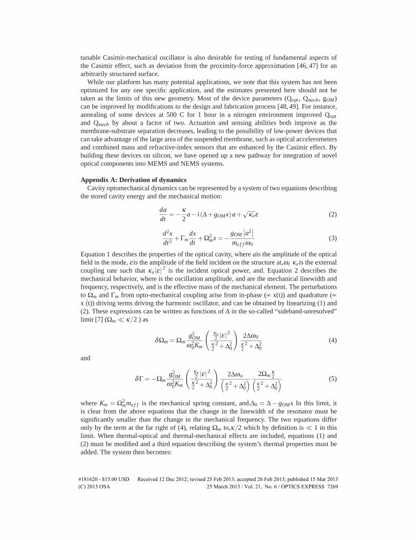
shown in the main paper and the curves in Fig. 6. We plot in Fig. 6 the Ωm and Γm dynamicsfor the deflected down device at four different optical powers: 6 μW (red circles), 12 μW(orange circles), 20 μW (yellow circles), and 100 μW (blue circles).The best fit parametersreveal a photo-thermal force which scales linearly with power, and thus corresponds to linearabsorption. However, the absorption rate Γabs seems to be larger than that expected from bulksilicon, most likely due to absorption from surface defects and surface adsorbents introducedduring the fabrication process [48, 49], though it is difficult to decouple Γabs from D and thusknow Γabs precisely. Measuring a set of devices before and after an annealing process seemed toconfirm this, as both the mechanical quality factor and optical quality factor improved slightlyafter baking. We can find an upper bound on Γabs by finding the rate at which the thermal-optic effect (last term in (12)) becomes notable, as our data reveals the effect to be quite smallin our system. From this, we can estimate a value of the absorption quality factor: (Qabs=ω0/Γabs≈ 105).
Fig. 6. Mechanical frequency and linewidth at four different power levels (colors cor-respond to colors in Fig. 5(c)). The same fit parameters were used in all fitting curves,demonstrating a quality fit across multiple data sets and powers on the same device. Notethat the fit to the photo-thermal-mechanical dynamics has linear power dependence, seenmost clearly in the Γm dynamics (bottom panel) thus demonstrating the lack of two-photonabsorption, which would have quadratic dependence.
Appendix B: FabricationFirst, two high resistivity Silicon-on Insulator (SOI) wafers (SOITEC, device layer thickness
= 220 nm, Buried Oxide (BOx) thickness = 2 μm) were thinned down using thermal oxida-tion, reducing the silicon device layer thickness to 185 nm. Next, oxide-oxide bonding was
#181620 - $15.00 USD Received 12 Dec 2012; revised 25 Feb 2013; accepted 26 Feb 2013; published 15 Mar 2013(C) 2013 OSA 25 March 2013 / Vol. 21, No. 6 / OPTICS EXPRESS 7272

used to bind the two wafers together. After low-stress nitride passivation, we then dry etchaway the backside of one of the handle silicon wafers using KOH to wet-etch the exposed han-dle silicon. This is followed by a Buffered Oxide (7:1 H20:HF) etch to remove the exposedbox layer to reveal two 185 nm silicon device layers separated by 260 nm of thermal oxide,above the 2 μm BOx layer. Devices patterns were then written using conventional 100 keVe-beam lithography on ZEP-520 positive photoresist and transferred to the top device layer us-ing inductively-coupled plasma reactive-ion etching. Finally, the oxide layer between the twoSi slabs is removed by Hydrogen Fluoride Vapor-phase Etching to release the top device layerand provide the gap between the top and bottom membrane. The process is described visuallyin Fig. 7(a). Annealing of some devices (data not shown) was performed at 500 C for 1 hour ina nitrogen environment in order to maximize optical and mechanical quality factors.
Fig. 7. (a) Fabrication process. Two SOI wafers are bonded together with an oxide-oxidebonding process, creating a sandwich structure with two thin silicon device layers in themiddle. SEM image of the sandwich shown in (b). Removal of one of the handle waferswith KOH and the thick oxide layer with BOE leaves a double-device layer chip, with thetwo Si layers separated by a 260 nm oxide gap. E-beam lithography followed by ReactiveIon Etching of the top silicon layer and HF Vapor Etching of the thermal-oxide gap layercreate the final device (last panel of (a)). (c): HFVE selectively etches at a higher rate alongthe oxide-oxide bond interface (red-dashed line) than it etches through the oxide layer,resulting in SiO2 residue along the Silicon surfaces.
A cross section of the layer stack taken using a Scanning Electron Microscope is shown inFig. 7(b). The whole process of thermal oxidation, oxide-oxide bonding, and removal of thehandle silicon results in stresses in the multi-thin film layer structure, which leads to bucklingof the silicon device layer when it is released. As a consequence of these processing and fabri-cation steps, we have also observed faster oxide HFVE rates in the bond-interface region thatresult in the presence of residual oxide close to the silicon membrane, which can be wider than1 μm at the edges of the etch area (Fig. 7(c)). A bending moment M‖ due to the residual stressin the device layer (curved purple lines, Fig. 8(a)i) causes a strong upward force on the devicesfabricated with simple arms (Fig. 2(a) and 8(b)i), forcing them to deflect by more than 300 nm.
#181620 - $15.00 USD Received 12 Dec 2012; revised 25 Feb 2013; accepted 26 Feb 2013; published 15 Mar 2013(C) 2013 OSA 25 March 2013 / Vol. 21, No. 6 / OPTICS EXPRESS 7273
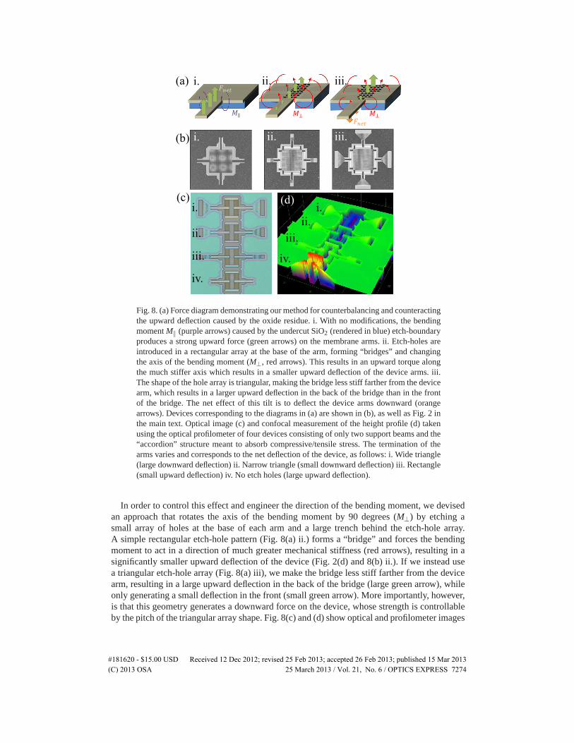
Fig. 8. (a) Force diagram demonstrating our method for counterbalancing and counteractingthe upward deflection caused by the oxide residue. i. With no modifications, the bendingmoment M‖ (purple arrows) caused by the undercut SiO2 (rendered in blue) etch-boundaryproduces a strong upward force (green arrows) on the membrane arms. ii. Etch-holes areintroduced in a rectangular array at the base of the arm, forming “bridges” and changingthe axis of the bending moment (M⊥, red arrows). This results in an upward torque alongthe much stiffer axis which results in a smaller upward deflection of the device arms. iii.The shape of the hole array is triangular, making the bridge less stiff farther from the devicearm, which results in a larger upward deflection in the back of the bridge than in the frontof the bridge. The net effect of this tilt is to deflect the device arms downward (orangearrows). Devices corresponding to the diagrams in (a) are shown in (b), as well as Fig. 2 inthe main text. Optical image (c) and confocal measurement of the height profile (d) takenusing the optical profilometer of four devices consisting of only two support beams and the“accordion” structure meant to absorb compressive/tensile stress. The termination of thearms varies and corresponds to the net deflection of the device, as follows: i. Wide triangle(large downward deflection) ii. Narrow triangle (small downward deflection) iii. Rectangle(small upward deflection) iv. No etch holes (large upward deflection).
In order to control this effect and engineer the direction of the bending moment, we devisedan approach that rotates the axis of the bending moment by 90 degrees (M⊥) by etching asmall array of holes at the base of each arm and a large trench behind the etch-hole array.A simple rectangular etch-hole pattern (Fig. 8(a) ii.) forms a “bridge” and forces the bendingmoment to act in a direction of much greater mechanical stiffness (red arrows), resulting in asignificantly smaller upward deflection of the device (Fig. 2(d) and 8(b) ii.). If we instead usea triangular etch-hole array (Fig. 8(a) iii), we make the bridge less stiff farther from the devicearm, resulting in a large upward deflection in the back of the bridge (large green arrow), whileonly generating a small deflection in the front (small green arrow). More importantly, however,is that this geometry generates a downward force on the device, whose strength is controllableby the pitch of the triangular array shape. Fig. 8(c) and (d) show optical and profilometer images
#181620 - $15.00 USD Received 12 Dec 2012; revised 25 Feb 2013; accepted 26 Feb 2013; published 15 Mar 2013(C) 2013 OSA 25 March 2013 / Vol. 21, No. 6 / OPTICS EXPRESS 7274

of structures made up of two device arms and two sets of accordion structures in the center. Asis clear in the images, the devices with the widest triangle etch-hole pattern (i.) generate thelargest downward deflection (blue color in (d)). The narrower triangle pattern (ii.) generates asmall downward deflection, the rectangular pattern (iii.) results in a small upward deflection,and the etch-hole free device (iv.) suffers from a large upward deflection.
Acknowledgments
This work was supported by the Defense Advanced Research Projects Agency (DARPA) undercontract no N66001-09-1-2070-DOD and NSF CAREER grants. This work was carried outin part through the use of Massachusetts Institute of Technology’s Microsystems TechnologyLaboratories, and in part at the Center for Nanoscale Systems (CNS) at Harvard University, amember of the National Nanotechnology Infrastructure Network (NNIN), which is supportedby the National Science Foundation (NSF) under NSF award no. ECS-0335765. Thanks toProfessor Rob Wood at Harvard University who owns the Olympus LEXT OLS4000 opticalprofilometer on which some of our measurements were performed. Additional thanks to AlexeiBelyanin, Oskar Painter, Daniel Ramos, Igor Lovchinsky and Romain Blanchard for helpfuldiscussions.
#181620 - $15.00 USD Received 12 Dec 2012; revised 25 Feb 2013; accepted 26 Feb 2013; published 15 Mar 2013(C) 2013 OSA 25 March 2013 / Vol. 21, No. 6 / OPTICS EXPRESS 7275