Quasi-two-dimensional optomechanical crystals with a...
12
Quasi-two-dimensional optomechanical crystals with a complete phononic bandgap Thiago P. Mayer Alegre, 1,2 Amir Safavi-Naeini, 1,2 Martin Winger, 1 Oskar Painter 1,∗ 1 Thomas J. Watson, Sr., Laboratory of Applied Physics, California Institute of Technology, Pasadena, CA 91125, USA 2 These authors contributed equally to this work. ∗ [email protected] http://copilot.caltech.edu Abstract: A fully planar two-dimensional optomechanical crystal formed in a silicon microchip is used to create a structure devoid of phonons in the GHz frequency range. A nanoscale photonic crystal cavity is placed inside the phononic bandgap crystal in order to probe the properties of the localized acoustic modes. By studying the trends in mechanical damping, mode density, and optomechanical coupling strength of the acoustic resonances over an array of structures with varying geo- metric properties, clear evidence of a complete phononic bandgap is shown. © 2011 Optical Society of America OCIS codes: (220.4880) Optomechanics; (230.5298) Photonic crystals; (230.1040) Acousto- optical devices. References and links 1. Z. Liu, X. Zhang, Y. Mao, Y. Y. Zhu, Z. Yang, C. T. Chan, and P. Sheng, “Locally Resonant Sonic Materials,” Science 289(5485), 1734–1736 (2000). 2. S. Yang, J. H. Page, Z. Liu, M. L. Cowan, C. T. Chan, and P. Sheng, “Ultrasound Tunneling through 3D Phononic Crystals,” Phys. Rev. Lett. 88(10), 104301 (2002). 3. W. Cheng, J. Wang, U. Jonas, G. Fytas, and N. Stefanou, “Observation and tuning of hypersonic bandgaps in colloidal crystals,” Nat. Mater. 5(10), 830–836 (2006). 4. A. V. Akimov, Y. Tanaka, A. B. Pevtsov, S. F. Kaplan, V. G. Golubev, S. Tamura, D. R. Yakovlev, and M. Bayer, “Hypersonic Modulation of Light in Three-Dimensional Photonic and Phononic Band-Gap Materials,” Phys. Rev. Lett. 101(3), 033902 (2008). 5. T. Gorishnyy, C. K. Ullal, M. Maldovan, G. Fytas, and E. L. Thomas, “Hypersonic Phononic Crystals,” Phys. Rev. Lett. 94(11), 115501 (2005). 6. S. Mohammadi, A. A. Eftekhar, W. D. Hunt, and A. Adibi, “High-Q micromechanical resonators in a two- dimensional phononic crystal slab,” Appl. Phys. Lett. 94(5), 051906 (2009). 7. Y. Wen, J. Sun, C. Dais, D. Grtzmacher, T. Wu, J. Shi, and C. Sun, “Three-dimensional phononic nanocrystal composed of ordered quantum dots,” Appl. Phys. Lett. 96(12), 123113 (2010). 8. S. Yang, J. H. Page, Z. Liu, M. L. Cowan, C. T. Chan, and P. Sheng, “Focusing of Sound in a 3D Phononic Crystal,” Phys. Rev. Lett. 93(2), 024301 (2004). 9. J. Gaofeng and S. Zhifei, “A new seismic isolation system and its feasibility study,” Earthq. Eng. Eng. Vib. 9(1), 75–82 (2010). 10. M. Eichenfield, J. Chan, R. M. Camacho, K. J. Vahala, and O. Painter, “Optomechanical crystals,” Nature 462(7269), 78–82 (2009). 11. M. Maldovan and E. L. Thomas, “Simultaneous localization of photons and phonons in two-dimensional periodic structures,” Appl. Phys. Lett. 88(25), 251907 (2006). #140027 - $15.00 USD Received 21 Dec 2010; revised 21 Feb 2011; accepted 22 Feb 2011; published 11 Mar 2011 (C) 2011 OSA 14 March 2011 / Vol. 19, No. 6 / OPTICS EXPRESS 5658
Transcript of Quasi-two-dimensional optomechanical crystals with a...
Quasi-two-dimensional optomechanicalcrystals with a complete phononic
bandgap
Thiago P. Mayer Alegre, 1,2 Amir Safavi-Naeini, 1,2 Martin Winger, 1
Oskar Painter 1,∗1Thomas J. Watson, Sr., Laboratory of Applied Physics, California Institute of Technology,
Pasadena, CA 91125, USA2 These authors contributed equally to this work.
http://copilot.caltech.edu
Abstract: A fully planar two-dimensional optomechanical crystalformed in a silicon microchip is used to create a structure devoid ofphonons in the GHz frequency range. A nanoscale photonic crystalcavity is placed inside the phononic bandgap crystal in order to probethe properties of the localized acoustic modes. By studying the trends inmechanical damping, mode density, and optomechanical coupling strengthof the acoustic resonances over an array of structures with varying geo-metric properties, clear evidence of a complete phononic bandgap is shown.
© 2011 Optical Society of America
OCIS codes: (220.4880) Optomechanics; (230.5298) Photonic crystals; (230.1040) Acousto-optical devices.
References and links1. Z. Liu, X. Zhang, Y. Mao, Y. Y. Zhu, Z. Yang, C. T. Chan, and P. Sheng, “Locally Resonant Sonic Materials,”
Science 289(5485), 1734–1736 (2000).2. S. Yang, J. H. Page, Z. Liu, M. L. Cowan, C. T. Chan, and P. Sheng, “Ultrasound Tunneling through 3D Phononic
Crystals,” Phys. Rev. Lett. 88(10), 104301 (2002).3. W. Cheng, J. Wang, U. Jonas, G. Fytas, and N. Stefanou, “Observation and tuning of hypersonic bandgaps in
colloidal crystals,” Nat. Mater. 5(10), 830–836 (2006).4. A. V. Akimov, Y. Tanaka, A. B. Pevtsov, S. F. Kaplan, V. G. Golubev, S. Tamura, D. R. Yakovlev, and M. Bayer,
“Hypersonic Modulation of Light in Three-Dimensional Photonic and Phononic Band-Gap Materials,” Phys.Rev. Lett. 101(3), 033902 (2008).
5. T. Gorishnyy, C. K. Ullal, M. Maldovan, G. Fytas, and E. L. Thomas, “Hypersonic Phononic Crystals,” Phys.Rev. Lett. 94(11), 115501 (2005).
6. S. Mohammadi, A. A. Eftekhar, W. D. Hunt, and A. Adibi, “High-Q micromechanical resonators in a two-dimensional phononic crystal slab,” Appl. Phys. Lett. 94(5), 051906 (2009).
7. Y. Wen, J. Sun, C. Dais, D. Grtzmacher, T. Wu, J. Shi, and C. Sun, “Three-dimensional phononic nanocrystalcomposed of ordered quantum dots,” Appl. Phys. Lett. 96(12), 123113 (2010).
8. S. Yang, J. H. Page, Z. Liu, M. L. Cowan, C. T. Chan, and P. Sheng, “Focusing of Sound in a 3D PhononicCrystal,” Phys. Rev. Lett. 93(2), 024301 (2004).
9. J. Gaofeng and S. Zhifei, “A new seismic isolation system and its feasibility study,” Earthq. Eng. Eng. Vib. 9(1),75–82 (2010).
10. M. Eichenfield, J. Chan, R. M. Camacho, K. J. Vahala, and O. Painter, “Optomechanical crystals,” Nature462(7269), 78–82 (2009).
11. M. Maldovan and E. L. Thomas, “Simultaneous localization of photons and phonons in two-dimensional periodicstructures,” Appl. Phys. Lett. 88(25), 251907 (2006).
#140027 - $15.00 USD Received 21 Dec 2010; revised 21 Feb 2011; accepted 22 Feb 2011; published 11 Mar 2011(C) 2011 OSA 14 March 2011 / Vol. 19, No. 6 / OPTICS EXPRESS 5658
12. M. Eichenfield, J. Chan, A. H. Safavi-Naeini, K. J. Vahala, and O. Painter, “Modeling dispersive coupling andlosses of localized optical and mechanical modes in optomechanical crystals,” Opt. Express 17(22), 20078–20098(2009).
13. S. Mohammadi, A. A. Eftekhar, A. Khelif, and A. Adibi, “Simultaneous two-dimensional phononic and photonicband gaps in opto-mechanical crystal slabs,” Opt. Express 18(9), 9164–9172 (2010).
14. A. H. Safavi-Naeini and O. Painter, “Design of optomechanical cavities and waveguides on a simultaneousbandgap phononic-photonic crystal slab,” Opt. Express 18(14), 14926–14943 (2010).
15. Y. Pennec, B. D. Rouhani, E. H. El Boudouti, C. Li, Y. El Hassouani, J. O. Vasseur, N. Papanikolaou, S. Bench-abane, V. Laude, and A. Martinez, “Simultaneous existence of phononic and photonic band gaps in periodiccrystal slabs,” Opt. Express 18(13), 14301–14310 (2010).
16. D. Chang and A. H. Safavi-Naeini, M. Hafezi, and O. Painter, “Slowing and stopping light using an optomechan-ical crystal array,” arXiv:1006.3829 (2010).
17. A. H. Safavi-Naeini and O. Painter, “Proposal for an Optomechanical Traveling Wave Phonon-Photon Transla-tor,” New J. Phys. 13, 013017 (2011).
18. R. H. Stolen and E. P. Ippen, “Raman gain in glass optical waveguides,” Appl. Phys. Lett. 22(276), 276–278(1973).
19. X. Zhang and R. Sooryakumar and K. Bussmann “Confinement and transverse standing acoustic resonances infree-standing membranes,” Phys. Rev. B 68, 115430 (2003).
20. W. Cheng, N. Gomopoulos, G. Fytas, T. Gorishnyy, J. Walish, E. L. Thomas, A. Hiltner and E. Bae, “PhononDispersion and Nanomechanical Properties of Periodic 1D Multilayer Polymer Films,” Nano Lett. 8(5), 1423-8(2008).
21. T. J. Kippenberg, H. Rokhsari, T. Carmon, A. Scherer, and K. J. Vahala, “Analysis of Radiation-Pressure InducedMechanical Oscillation of an Optical Microcavity,” Phys. Rev. Lett. 95(3), 033,901–033,901 (2005).
22. Q. Lin, J. Rosenberg, X. Jiang, K. J. Vahala, and O. Painter, “Mechanical Oscillation and Cooling Actuated bythe Optical Gradient Force,” Phys. Rev. Lett. 103(10), 103601 (2009).
23. M. Eichenfield, R. Camacho, J. Chan, K. J. Vahala, and O. Painter, “A picogram- and nanometre-scale photonic-crystal optomechanical cavity,” Nature 459(7246), 550–555 (2009).
24. G. S. Wiederhecker, A. Brenn, H. L. Fragnito, and P. S. J. Russell, “Coherent Control of Ultrahigh-FrequencyAcoustic Resonances in Photonic Crystal Fibers,” Phys. Rev. Lett. 100(20), 203903 (2008).
25. K. L. Ekinci and M. L. Roukes, “Nanoelectromechanical systems,” Rev. Sci. Instrum. 76(6), 061101–061101(2005).
26. C. T. C. Nguyen, “MEMS technology for timing and frequency control,” IEEE Trans Ultrason Ferroelectr FreqControl 54(2), 251–270 (2007).
27. H. Campanella, Acoustic Wave and Electromechanical Resonators: Concept to Key Applications (Artech HousePublishers, 2010).
28. B. Song, S. Noda, T. Asano, and Y. Akahane, “Ultra-high-Q photonic double-heterostructure nanocavity,” Nat.Mater 4(3), 207–210 (2005).
29. M. Borselli, T. J. Johnson, and O. Painter, “Measuring the role of surface chemistry in silicon microphotonics,”Appl. Phys. Lett. 88(13), 131,114–3 (2006).
30. COMSOL Multphysics 3.5 (2009).31. A. Akhieser, J. Phys. (Moscow) 1, 277 (1939).32. L. Landau and G. Rumer, “Absorption of sound in solids,” Phys. Z. Sowjetunion 11, 18 (1937).33. C. Zener, “Internal Friction in Solids II. General Theory of Thermoelastic Internal Friction,” Phys. Rev. 53(1),
90 (1938).34. S. D. Lambade, G. G. Sahasrabudhe, and S. Rajagopalan, “Temperature dependence of acoustic attenuation in
silicon,” Phys. Rev. B 51(22), 15,861 (1995).35. C. Zener, “Internal Friction in Solids. I. Theory of Internal Friction in Reeds,” Phys. Rev. 52(3), 230 (1937).36. R. Lifshitz and M. L. Roukes, “Thermoelastic damping in micro- and nanomechanical systems,” Phys. Rev. B
61(8), 5600 (2000).37. T. O. Woodruff and H. Ehrenreich, “Absorption of Sound in Insulators,” Phys. Rev. 123(5), 1553 (1961).38. J. Philip and M. A. Breazeale, “Third-order elastic constants and Gruneisen parameters of silicon and germanium
between 3 and 300 K,” J. Appl. Phys. 54(2), 752 (1983).39. S. K. Estreicher, M. Sanati, D. West, and F. Ruymgaart, “Thermodynamics of impurities in semiconductors,”
Phys. Rev. B 70(12), 125209 (2004).40. A. Duwel, R. Candler, T. Kenny, and M. Varghese, “Engineering MEMS Resonators With Low Thermoelastic
Damping,” J. Microelectromech. Syst. 15(6), 1437–1445 (2006).
1. Introduction
Photonic crystals are periodic dielectric structures in which optical waves encounter strongdispersion, and in some cases are completely forbidden from propagating within a frequency
#140027 - $15.00 USD Received 21 Dec 2010; revised 21 Feb 2011; accepted 22 Feb 2011; published 11 Mar 2011(C) 2011 OSA 14 March 2011 / Vol. 19, No. 6 / OPTICS EXPRESS 5659

bandgap. Similarly, periodic elastic structures, known as phononic crystals, can be used to con-trol acoustic waves [1–7] for applications as diverse as the filtering and focusing of sound [8] tothe earthquake proofing of buildings [9]. Recently, microchip structures capable of manipulat-ing both photons and phonons, dubbed optomechanical crystals (OMCs), have been created toenhance the interaction of light and mechanics [10–15]. Here we use a planar two-dimensional(2D) OMC to create a structure devoid of phonons in the GHz frequency range, and use lightto probe its mechanical properties. In addition to being an excellent platform for the studyof radiation pressure and nanomechanics, the 2D-OMC of this work represents an importantstep towards more complex devices capable of performing novel classical and quantum opticalsignal processing [16, 17].
Interest in cavity-optomechanical systems, in which light is used to sensitively measure andmanipulate the motion of a mechanically compliant optical cavity, has grown rapidly in the lastfew years due to the demonstration of micro- and nano-scale systems in which the radiationpressure force of light is manifest. The physics of these systems is formally equivalent to theinelastic scattering of light by bulk elastic vibrations (Brillouin scattering), and has been stud-ied in a variety of settings [18–20]. In cavity optomechanics, the presence of both mechanicaland optical resonances brings about qualitatively new effects, and has been the subject of re-cent intense study. In its most basic form, the mechanical resonance has been that of movableend-mirror affixed to a spring (or hung as a pendulum), forming part of a Fabry-Perot cav-ity. More complex cavity-optomechanical geometries, such as whispering-gallery mode struc-tures [21, 22], nanomembranes placed within Fabry-Perot cavities, and near-field optical andmicrowave devices utilizing the gradient force [23], have also been demonstrated to producestrong radiation pressure effects. Two structures with particular engineerability of optical andmechanical properties are the photonic crystal fiber (PCF) [24] and the recently demonstratedchip-scale optomechanical crystal (OMC) [10]. In the case of the OMC cavity, a patterning ofa silicon (Si) nanobeam is used to create a 200 THz optical cavity simultaneous with a GHzacoustic cavity.
In the last decade, Si photonics has rapidly developed, in no small part due to the adventof silicon-on-insulator wafer technology in which a thin Si device layer sits atop a low-indexinsulating oxide layer. Planar Si photonic crystal circuits may be formed in the top Si devicelayer, which along with the integrability with micro-electronics, has provided an attractive set-ting for controlling photons. Similarly, in the case of phononics, significant progress has beenmade in integrated Si MEMS and NEMS devices for creating RF/microwave filters, oscillators,and sensors [25–27]. Thin-film OMCs bring together photonic and phononic circuitry, enablinga new chip-scale platform for delaying, storing, and processing optical and acoustic excita-tions [16, 17]. Building on our previous work in quasi-1D OMC systems [10], we demonstratehere a quasi-2D OMC architecture capable of routing photons and phonons around the full2D plane of a Si chip, and enabling complete localization of phonons via a three-dimensionalacoustic-wave bandgap.
2. Sample structure
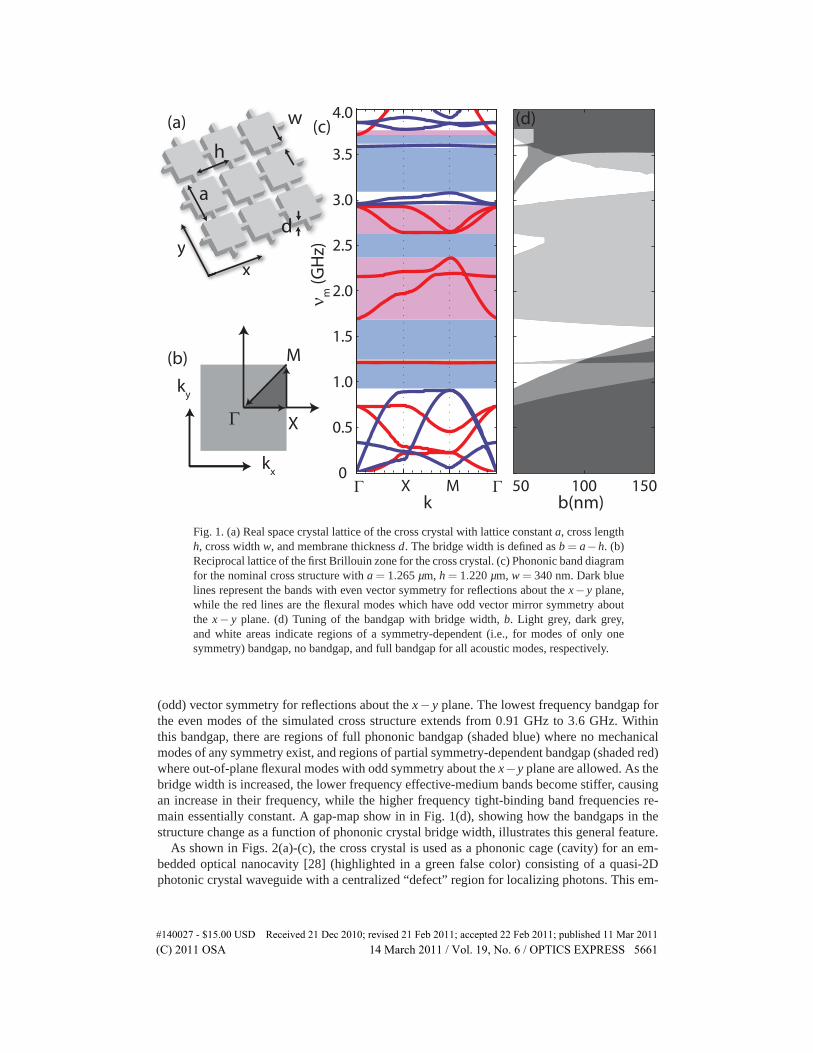
The phononic crystal used in this work is the recently proposed [14] “cross” structure shown inFig. 1(a). Geometrically, the structure consists of an array of squares connected to each otherby thin bridges, or equivalently, a square lattice of cross-shaped holes. The phononic bandgapin this structure arises from the frequency separation between higher frequency tight-bindingbands, which have similar frequencies to the resonances of the individual squares, and lowerfrequency effective-medium bands with frequencies strongly dependent on the width of the con-necting bridges, b = a−h [14]. A typical band diagram for a nominal structure (a = 1.265 µm,h = 1.220 µm, w = 340 nm) is shown in Fig. 1(c). Blue (red) lines represent bands with even
#140027 - $15.00 USD Received 21 Dec 2010; revised 21 Feb 2011; accepted 22 Feb 2011; published 11 Mar 2011(C) 2011 OSA 14 March 2011 / Vol. 19, No. 6 / OPTICS EXPRESS 5660
50 100 150
(c)
(b)
(a) (d)
Γ X M Γ0
0.5
1.0
1.5
2.0
2.5
3.0
3.5
4.0
k
ν m (G
Hz)
b(nm)
XΓ
M
ky
kx
(c)(a)
Hz)
h
a
yxxxxx
yd
w
Fig. 1. (a) Real space crystal lattice of the cross crystal with lattice constant a, cross lengthh, cross width w, and membrane thickness d. The bridge width is defined as b = a−h. (b)Reciprocal lattice of the first Brillouin zone for the cross crystal. (c) Phononic band diagramfor the nominal cross structure with a = 1.265 µm, h = 1.220 µm, w = 340 nm. Dark bluelines represent the bands with even vector symmetry for reflections about the x− y plane,while the red lines are the flexural modes which have odd vector mirror symmetry aboutthe x− y plane. (d) Tuning of the bandgap with bridge width, b. Light grey, dark grey,and white areas indicate regions of a symmetry-dependent (i.e., for modes of only onesymmetry) bandgap, no bandgap, and full bandgap for all acoustic modes, respectively.
(odd) vector symmetry for reflections about the x− y plane. The lowest frequency bandgap forthe even modes of the simulated cross structure extends from 0.91 GHz to 3.6 GHz. Withinthis bandgap, there are regions of full phononic bandgap (shaded blue) where no mechanicalmodes of any symmetry exist, and regions of partial symmetry-dependent bandgap (shaded red)where out-of-plane flexural modes with odd symmetry about the x−y plane are allowed. As thebridge width is increased, the lower frequency effective-medium bands become stiffer, causingan increase in their frequency, while the higher frequency tight-binding band frequencies re-main essentially constant. A gap-map show in in Fig. 1(d), showing how the bandgaps in thestructure change as a function of phononic crystal bridge width, illustrates this general feature.
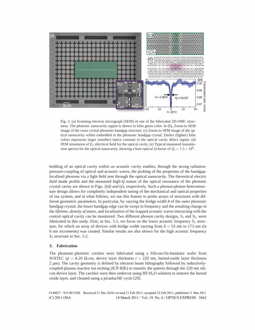
As shown in Figs. 2(a)-(c), the cross crystal is used as a phononic cage (cavity) for an em-bedded optical nanocavity [28] (highlighted in a green false color) consisting of a quasi-2Dphotonic crystal waveguide with a centralized “defect” region for localizing photons. This em-
#140027 - $15.00 USD Received 21 Dec 2010; revised 21 Feb 2011; accepted 22 Feb 2011; published 11 Mar 2011(C) 2011 OSA 14 March 2011 / Vol. 19, No. 6 / OPTICS EXPRESS 5661
(a)
(d)
-20 -10 0 10 20
0.97
0.98
0.99
1.00
(pm)
Transm
ission
(arb. u
nits)
1.0pm Qi=1.5x10⁶
(e)
(c)
1m
2m-2-2-20-2
yx
b
aw
h
400nm
(b)
Fig. 2. (a) Scanning electron micrograph (SEM) of one of the fabricated 2D-OMC struc-tures. The photonic nanocavity region is shown in false green color. In (b), Zoom-in SEMimage of the cross crystal phononic bandgap structure. (c) Zoom-in SEM image of the op-tical nanocavity within embedded in the phononic bandgap crystal. Darker (lighter) falsecolors represents larger (smaller) lattice constant in the optical cavity defect region. (d)FEM simulation of Ey electrical field for the optical cavity. (e) Typical measured transmis-sion spectra for the optical nanocavity, showing a bare optical Q-factor of Qi = 1.5×10⁶.
bedding of an optical cavity within an acoustic cavity enables, through the strong radiation-pressure-coupling of optical and acoustic waves, the probing of the properties of the bandgap-localized phonons via a light field sent through the optical nanocavity. The theoretical electricfield mode profile and the measured high-Q nature of the optical resonance of the photoniccrystal cavity are shown in Figs. 2(d) and (e), respectively. Such a phonon-photon heterostruc-ture design allows for completely independent tuning of the mechanical and optical propertiesof our system, and in what follows, we use this feature to probe arrays of structures with dif-ferent geometric parameters. In particular, by varying the bridge width b of the outer phononicbandgap crystal, the lower bandgap edge can be swept in frequency and the resulting change inthe lifetime, density of states, and localization of the trapped acoustic waves interacting with thecentral optical cavity can be monitored. Two different phonon cavity designs, S1 and S2, werefabricated in this study. First, in Sec. 5.1, we focus on the lower acoustic frequency S1 struc-ture, for which an array of devices with bridge width varying from b = 53 nm to 173 nm (in6 nm increments) was created. Similar results are also shown for the high acoustic frequencyS2 structure in Sec. 5.2.
3. Fabrication
The phononic-photonic cavities were fabricated using a Silicon-On-Insulator wafer fromSOITEC (ρ = 4-20 Ω·cm, device layer thickness t = 220 nm, buried-oxide layer thickness2 µm). The cavity geometry is defined by electron beam lithography followed by inductively-coupled-plasma reactive ion etching (ICP-RIE) to transfer the pattern through the 220 nm sili-con device layer. The cavities were then undercut using HF:H2O solution to remove the buriedoxide layer, and cleaned using a piranha/HF cycle [29].
#140027 - $15.00 USD Received 21 Dec 2010; revised 21 Feb 2011; accepted 22 Feb 2011; published 11 Mar 2011(C) 2011 OSA 14 March 2011 / Vol. 19, No. 6 / OPTICS EXPRESS 5662
4. Experimental setup
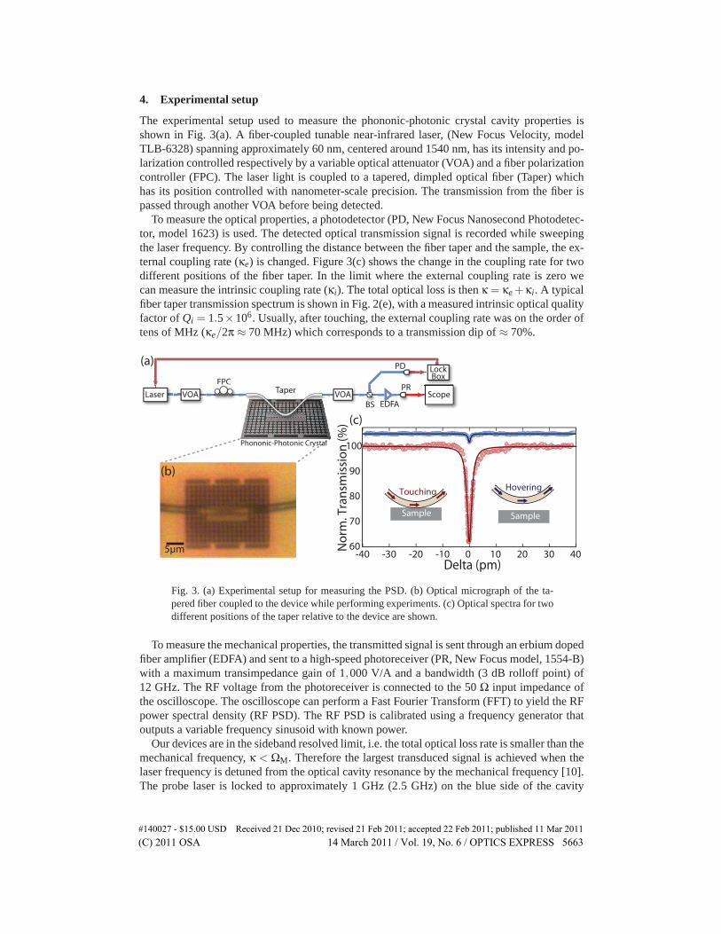
The experimental setup used to measure the phononic-photonic crystal cavity properties isshown in Fig. 3(a). A fiber-coupled tunable near-infrared laser, (New Focus Velocity, modelTLB-6328) spanning approximately 60 nm, centered around 1540 nm, has its intensity and po-larization controlled respectively by a variable optical attenuator (VOA) and a fiber polarizationcontroller (FPC). The laser light is coupled to a tapered, dimpled optical fiber (Taper) whichhas its position controlled with nanometer-scale precision. The transmission from the fiber ispassed through another VOA before being detected.
To measure the optical properties, a photodetector (PD, New Focus Nanosecond Photodetec-tor, model 1623) is used. The detected optical transmission signal is recorded while sweepingthe laser frequency. By controlling the distance between the fiber taper and the sample, the ex-ternal coupling rate (κe) is changed. Figure 3(c) shows the change in the coupling rate for twodifferent positions of the fiber taper. In the limit where the external coupling rate is zero wecan measure the intrinsic coupling rate (κi). The total optical loss is then κ = κe +κi. A typicalfiber taper transmission spectrum is shown in Fig. 2(e), with a measured intrinsic optical qualityfactor of Qi = 1.5×10⁶. Usually, after touching, the external coupling rate was on the order oftens of MHz (κe/2π ≈ 70 MHz) which corresponds to a transmission dip of ≈ 70%.
EDFA
FPCTaper
Phononic-Photonic Crystal
5µm
(a)
(b)
(c)
Sample
Hovering
Sample
Touching
-40 -30 -20 -10 0 20 40301060
70
80
90
100
Delta (pm)
No
rm. T
ran
smis
sio
n (%
)
PD
BS
PR
DD
A
PRLaser Scope
BSBSVOA VOA
LockBox
FPC
Fig. 3. (a) Experimental setup for measuring the PSD. (b) Optical micrograph of the ta-pered fiber coupled to the device while performing experiments. (c) Optical spectra for twodifferent positions of the taper relative to the device are shown.
To measure the mechanical properties, the transmitted signal is sent through an erbium dopedfiber amplifier (EDFA) and sent to a high-speed photoreceiver (PR, New Focus model, 1554-B)with a maximum transimpedance gain of 1,000 V/A and a bandwidth (3 dB rolloff point) of12 GHz. The RF voltage from the photoreceiver is connected to the 50 Ω input impedance ofthe oscilloscope. The oscilloscope can perform a Fast Fourier Transform (FFT) to yield the RFpower spectral density (RF PSD). The RF PSD is calibrated using a frequency generator thatoutputs a variable frequency sinusoid with known power.
Our devices are in the sideband resolved limit, i.e. the total optical loss rate is smaller than themechanical frequency, κ < ΩM. Therefore the largest transduced signal is achieved when thelaser frequency is detuned from the optical cavity resonance by the mechanical frequency [10].The probe laser is locked to approximately 1 GHz (2.5 GHz) on the blue side of the cavity
#140027 - $15.00 USD Received 21 Dec 2010; revised 21 Feb 2011; accepted 22 Feb 2011; published 11 Mar 2011(C) 2011 OSA 14 March 2011 / Vol. 19, No. 6 / OPTICS EXPRESS 5663
resonance for the S1 (S2) structures. By measuring the transmission contrast during the acqui-sition of the RF PSD and comparing with the transmission curve of each device (as shown inFig. 3(c)) we determine the laser detuning and the dropped power into the cavity. To lock theprobe laser frequency a given frequency away from the resonance, a 90/10 beam splitter (BS)is added to the optical path, and the signal from the 10% arm is fed to a PD connected to a lock-ing circuit which compares the voltage level from the transmission signal to a predeterminedvalue to generate an error signal. The error signal is then fed to a piezoelectric actuator on thefeedback grating of the laser in order to stabilize the laser frequency.
5. Results and discussion
5.1. Phononic band gap: sample S1
0 0.2 0.4 0.6 0.8 1.0 1.2 1.4 1.6
-86
-85
-84
-83
RF P
SD (d
Bm
)
-86
-82
-78
-82
-78
-74
1.385 1.39 1.395
b=57nm
b=106nm
b=160nm
νM
(GHz)νM
(GHz)
T = 10K
T = 20K
T = 30K
T = 50K
T = 100K
T = 300K
QM
= 1.3x10⁴
QM
= 6.4x10³
QM
= 7.8x10³
QM
= 7.1x10³
QM
= 5.5x10³
QM
= 3.3x10³
(a) (b)
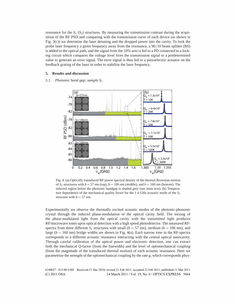
Fig. 4. (a) Optically transduced RF power spectral density of the thermal Brownian motionof S1 structures with b = 57 nm (top), b = 106 nm (middle), and b = 160 nm (bottom). Theinferred region below the phononic bandgap is shaded grey (see main text). (b) Tempera-ture dependence of the mechanical quality factor for the 1.4 GHz acoustic mode of the S1structure with b = 57 nm.
Experimentally we observe the thermally excited acoustic modes of the photonic-phononiccrystal through the induced phase-modulation of the optical cavity field. The mixing ofthe phase-modulated light from the optical cavity with the transmitted light producesRF/microwave tones upon optical detection with a high speed photodetector. The measured RF-spectra from three different S1 structures with small (b = 57 nm), medium (b = 106 nm), andlarge (b = 160 nm) bridge widths are shown in Fig. 4(a). Each narrow tone in the RF-spectracorresponds to a different acoustic resonance interacting with the central optical nanocavity.Through careful calibration of the optical power and electronic detection, one can extractboth the mechanical Q-factor (from the linewidth) and the level of optomechanical coupling(from the magnitude of the transduced thermal motion) of each acoustic resonance. Here weparametrize the strength of the optomechanical coupling by the rate g, which corresponds phys-
#140027 - $15.00 USD Received 21 Dec 2010; revised 21 Feb 2011; accepted 22 Feb 2011; published 11 Mar 2011(C) 2011 OSA 14 March 2011 / Vol. 19, No. 6 / OPTICS EXPRESS 5664

1005050 150b (nm)
100 150b (nm)
0.8
1.0
1.2
1.4
1.6
1.8
Freq
uen
cy (G
Hz)
(a) (b)
(e)(f)
g/2π
(kH
z)
80 120 160b(nm)
0
10
20
30
40
νM
(GHz)
10
20
30
40
0.8 1.0 1.2 1.4 1.6
0
20
40
60
0
20
60
40
x1
x110
(c) (d)
Fig. 5. (a) Plot of the 3D-FEM simulated in-plane localized acoustic modes of the S1 struc-ture as a function of bridge width b. Each marker corresponds to a single acoustic mode,with the marker size proportional to the logarithm of the calculated acoustic radiation Q-factor. The light blue shaded markers correspond to acoustic bands which are opticallydark. The shading corresponds to the same color coding of the phononic bandgaps as thatused in Fig. 1(d). (b) Measured mode plot of the optically-transduced localized acousticmodes for an array of S1 structures with varying bridge width. The marker size of eachresonance is related to the logarithm of the measured mechanical Q-factor. The inferredspectral region below the phononic bandgap is shaded grey. (c) and (d) FEM simulationsof the displacement field amplitude (|Q(r)|) for the acoustic mode in the orange coloredband around 1.35 GHz in (a). In (c) the mode is within the phononic band gap resulting ina radiation-limited Q(rad)
M ≈ 109. In (d) the mode is on the edge of the bandgap and has a
reduced Q(rad)M < 103. (e) Simulated (�) and measured (◦) optomechanical coupling rate g
for the orange (red) highlighted acoustic band in (a) ((b)). (f) Simulated (�) and measured(◦) optomechanical coupling rate g for the series of acoustic modes of the S1 structure withb ∼ 100 nm (vertical dashed curves in (a) and (b))
ically to the shift in the optical cavity resonance frequency due to the zero-point motion of theacoustic resonance [14]. A measurement of the temperature dependence of the acoustic modespectrum is also performed, and is shown in Fig. 4(b) for one of the acoustic resonances over atemperature range from 300 K to 10 K.
By measuring the entire set of S1 devices in this way, a map may be produced of the localizedacoustic modes’ properties versus bridge width. In Figs. 5(a) and 5(b) we plot the numericallysimulated and experimentally measured mode map for the S1 structure. Each marker in theseplots corresponds to a different acoustic resonance, with the position of the marker indicatingthe mode frequency and the size of the marker indicating the mechanical Q-factor of the mode(for the numerical simulations all mechanical Q-factors above 107 are shown with the samemarker size). Numerical simulations of the optical, mechanical, and optomechanical propertiesof the structure are performed using the COMSOL [30] finite-element-method (FEM) soft-ware package, with an absorbing boundary condition applied at the exterior of the phononic
#140027 - $15.00 USD Received 21 Dec 2010; revised 21 Feb 2011; accepted 22 Feb 2011; published 11 Mar 2011(C) 2011 OSA 14 March 2011 / Vol. 19, No. 6 / OPTICS EXPRESS 5665
cage [12]. The various bandgap regions are indicated in Fig. 5(a) with the same color codingas in Fig. 1(c). Due to the weak radiation pressure coupling to the optical nanocavity of theflexure acoustic modes of odd symmetry about the x-y plane of the slab (red mode bands inFig. 1(c)), we only show in the simulated mode plot of Fig. 5(a) the even symmetry, in-planeacoustic resonances.
The striking similarity of the simulated and measured mode plots is evidence that the opticalnanocavity is able to sensitively probe the in-plane localized acoustic modes of the phononicbandgap structure (the acoustic band with light blue marker in Fig. 5(a) is the one localizedin-plane mode which does not show up in the measured plot of Fig. 5(b); numerical simulationsshow this mode to be a surface mode at the inner edge of the cross crystal, which does not coupleto the central optical cavity). Within the bandgap, modes are tightly localized (see Fig. 5(c)) anddo not radiate acoustic energy, whereas below the bandgap the acoustic modes spread into theexterior cross crystal (see Fig. 5(d)), leaking energy into the surrounding substrate region. Theboundary where the mechanical Q-factor drops off is clearly identifiable in the experimentallymeasured mode plot of Fig. 5(b) (the spectral region below the apparent full phononic bandgapis shaded grey as a guide to the eye), and matches up well with the theoretical lower frequencyband-edge of the full phononic bandgap of the cross crystal.
Two other distinguishing features between modes inside and outside a bandgap are thespectral mode density and the strength of the optomechanical coupling. Below the phononicbandgap, acoustic modes can fill the entire volume of the cross crystal (out to the boundary ofthe undercut structure where it is finally clamped), resulting in an increase of the mode density(proportional to volume) and a decrease in the optomechanical coupling (proportional to theinverse-square-root of mode volume [14]). In Fig. 5(e) we have plotted the theoretically com-puted and experimentally measured values of the optomechancial coupling (g) for an acousticresonance lying near the middle of the full phononic bandgap (this resonance is highlightedin orange in the theoretical plot of Fig. 5(a) and red in the measured plot of Fig. 5(b)). Themeasured trend of optomechanical coupling nicely matches that of the theoretical one, andhighlights the sharp drop off in optomechanical coupling as the mode crosses the bandgap.Similarly, in Fig. 5(f) we plot the optomechanical coupling for the acoustic resonances of asingle device with bridge width b ∼ 100 nm (corresonding to a vertical slice in Figs. 5(a) and5(b) as indicated by a dashed vertical line). Again we see good correspondence between theoryand experiment, with the drop off in g and the large increase in spectral mode density clearlyevident in both plots below the bandgap (note that the frequency position of the bandgap edgeis not the same in the theoretical and experimental plots of Figs. 5(e) and 5(f) due to the slightdifferences in bridge width).
Finally we note the high sensitivity of the most strongly transduced modes, by analyzingthe spectra shown in Fig. 4. The room temperature sensitivity of the mechanical mode wascalculated to be 5.0× 10⁻¹⁷m/
√Hz. This sensitivity increases to 2.5× 10⁻¹⁷m/
√Hz at low
temperatures (8.7 K), due to a four-fold increase in mechanical Q.
5.2. Phononic band gap: sample S2
In this section we present measurements performed on a second design (S2) with phononicbandgap in a different frequency range. Following the nomenclature in Fig. 1, the nominaldimensions for the S2 devices are: a = 925 nm, h = 850 nm, and w = 210 nm, which allows foran acoustic bandgap around 1.6 to 2.5 GHz. The optical nanocavity in the S2 devices are thesame as that used in S1 devices.
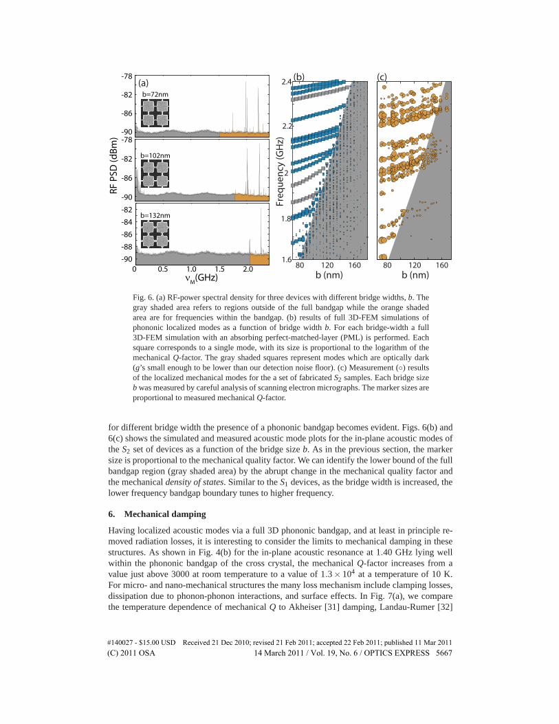
To show the presence of a bandgap, we fabricate and measure a set of devices with bridgewidths varying from 70 to 170 nm. The RF PSD of the optically transmitted signal is shown inFig. 6(a) for three different S2 structures with different bridge widths. By comparing the spectra
#140027 - $15.00 USD Received 21 Dec 2010; revised 21 Feb 2011; accepted 22 Feb 2011; published 11 Mar 2011(C) 2011 OSA 14 March 2011 / Vol. 19, No. 6 / OPTICS EXPRESS 5666
Freq
uen
cy (G
Hz)
(a)(b) (c)
b (nm)80 120 160
1.6
1.8
2
2.2
2.4
80 120 160b (nm)
-90
-86
-82
-78
-90
-86
-82
-78
RF P
SD (d
Bm
)
0 0.5 1.0 1.5 2.0-90
-88
-86
-84
-82
b=72nm
b=102nm
b=132nm
νM
(GHz)
Fig. 6. (a) RF-power spectral density for three devices with different bridge widths, b. Thegray shaded area refers to regions outside of the full bandgap while the orange shadedarea are for frequencies within the bandgap. (b) results of full 3D-FEM simulations ofphononic localized modes as a function of bridge width b. For each bridge-width a full3D-FEM simulation with an absorbing perfect-matched-layer (PML) is performed. Eachsquare corresponds to a single mode, with its size is proportional to the logarithm of themechanical Q-factor. The gray shaded squares represent modes which are optically dark(g’s small enough to be lower than our detection noise floor). (c) Measurement (◦) resultsof the localized mechanical modes for the a set of fabricated S2 samples. Each bridge sizeb was measured by careful analysis of scanning electron micrographs. The marker sizes areproportional to measured mechanical Q-factor.
for different bridge width the presence of a phononic bandgap becomes evident. Figs. 6(b) and6(c) shows the simulated and measured acoustic mode plots for the in-plane acoustic modes ofthe S2 set of devices as a function of the bridge size b. As in the previous section, the markersize is proportional to the mechanical quality factor. We can identify the lower bound of the fullbandgap region (gray shaded area) by the abrupt change in the mechanical quality factor andthe mechanical density of states. Similar to the S1 devices, as the bridge width is increased, thelower frequency bandgap boundary tunes to higher frequency.
6. Mechanical damping
Having localized acoustic modes via a full 3D phononic bandgap, and at least in principle re-moved radiation losses, it is interesting to consider the limits to mechanical damping in thesestructures. As shown in Fig. 4(b) for the in-plane acoustic resonance at 1.40 GHz lying wellwithin the phononic bandgap of the cross crystal, the mechanical Q-factor increases from avalue just above 3000 at room temperature to a value of 1.3× 10⁴ at a temperature of 10 K.For micro- and nano-mechanical structures the many loss mechanism include clamping losses,dissipation due to phonon-phonon interactions, and surface effects. In Fig. 7(a), we comparethe temperature dependence of mechanical Q to Akheiser [31] damping, Landau-Rumer [32]
#140027 - $15.00 USD Received 21 Dec 2010; revised 21 Feb 2011; accepted 22 Feb 2011; published 11 Mar 2011(C) 2011 OSA 14 March 2011 / Vol. 19, No. 6 / OPTICS EXPRESS 5667
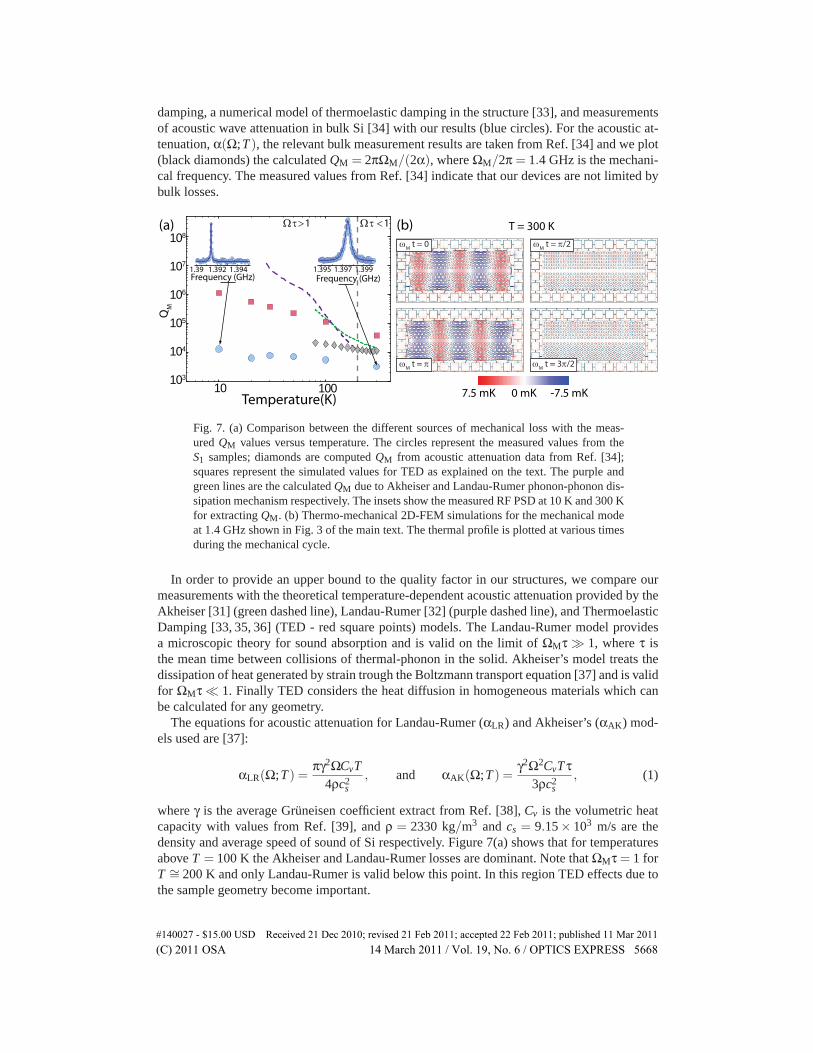
damping, a numerical model of thermoelastic damping in the structure [33], and measurementsof acoustic wave attenuation in bulk Si [34] with our results (blue circles). For the acoustic at-tenuation, α(Ω;T ), the relevant bulk measurement results are taken from Ref. [34] and we plot(black diamonds) the calculated QM = 2πΩM/(2α), where ΩM/2π = 1.4 GHz is the mechani-cal frequency. The measured values from Ref. [34] indicate that our devices are not limited bybulk losses.
7.5 mK 0 mK -7.5 mK
M
t = 0 M
t = /2
M
t = M
t = 3/2
T = 300 K
1.39 1.3941.392Frequency (GHz) Frequency (GHz)
1.3991.395 1.397
10 100103
104
105
106
107
108
Temperature(K)
QM
1 1(a) (b)
Fig. 7. (a) Comparison between the different sources of mechanical loss with the meas-ured QM values versus temperature. The circles represent the measured values from theS1 samples; diamonds are computed QM from acoustic attenuation data from Ref. [34];squares represent the simulated values for TED as explained on the text. The purple andgreen lines are the calculated QM due to Akheiser and Landau-Rumer phonon-phonon dis-sipation mechanism respectively. The insets show the measured RF PSD at 10 K and 300 Kfor extracting QM. (b) Thermo-mechanical 2D-FEM simulations for the mechanical modeat 1.4 GHz shown in Fig. 3 of the main text. The thermal profile is plotted at various timesduring the mechanical cycle.
In order to provide an upper bound to the quality factor in our structures, we compare ourmeasurements with the theoretical temperature-dependent acoustic attenuation provided by theAkheiser [31] (green dashed line), Landau-Rumer [32] (purple dashed line), and ThermoelasticDamping [33, 35, 36] (TED - red square points) models. The Landau-Rumer model providesa microscopic theory for sound absorption and is valid on the limit of ΩMτ � 1, where τ isthe mean time between collisions of thermal-phonon in the solid. Akheiser’s model treats thedissipation of heat generated by strain trough the Boltzmann transport equation [37] and is validfor ΩMτ � 1. Finally TED considers the heat diffusion in homogeneous materials which canbe calculated for any geometry.
The equations for acoustic attenuation for Landau-Rumer (αLR) and Akheiser’s (αAK) mod-els used are [37]:
αLR(Ω;T ) =πγ2ΩCvT
4ρc2s
, and αAK(Ω;T ) =γ2Ω2CvTτ
3ρc2s
, (1)
where γ is the average Gruneisen coefficient extract from Ref. [38], Cv is the volumetric heatcapacity with values from Ref. [39], and ρ = 2330 kg/m3 and cs = 9.15× 10³ m/s are thedensity and average speed of sound of Si respectively. Figure 7(a) shows that for temperaturesabove T = 100 K the Akheiser and Landau-Rumer losses are dominant. Note that ΩMτ = 1 forT ∼= 200 K and only Landau-Rumer is valid below this point. In this region TED effects due tothe sample geometry become important.
#140027 - $15.00 USD Received 21 Dec 2010; revised 21 Feb 2011; accepted 22 Feb 2011; published 11 Mar 2011(C) 2011 OSA 14 March 2011 / Vol. 19, No. 6 / OPTICS EXPRESS 5668
Our approach for calculating TED follows that of Ref. [40], where the TED-limited QM,TED
is extracted from 2D-FEM simulations [30] for the thermo-mechanical equations consideringa finite thickness. Figure 7(b) shows the change in temperature, ΔT (r) = T − To, for the de-formed structure, versus the phase of the mechanical oscillations, at the expected brownianmotion amplitude for To = 300 K. The temperature difference was calculated based on the max-
imum thermal displacement amplitude xmax =√
2kTo/meffΩ2M . These plots show that during a
mechanical cycle, even when there is no deformation, i.e. ΩMt = π/2 and 3π/2, the tempera-ture gradient is non-zero. This indicates that the temperature does not follow adiabatically thestrain/stress profile, causing a time-delayed force to be imparted on the resonator, and leadingto dissipation.
The measured temperature dependence and the overall magnitude of the measured mechani-cal Q-factor are seen to be much smaller than any of these comparisons, suggesting that surfaceeffects and/or fabrication-induced damage may be playing an important role in the mechanicaldamping of the nanostructured devices studied here.
7. Conclusion
Beyond the confinement and localization of acoustic modes in three dimensions, the connectedgeometry of the 2D-OMC structures presented in this work offers a platform for more com-plex phonon-photon circuitry. As has been described in recent theoretical analyses [14, 16, 17],such circuitry could be used to create optomechanical systems with greatly enhanced optome-chanical coupling, and to realize devices such as traveling wave phonon-photon translators andslow light waveguides capable of advanced classical and quantum optical signal processing.The functionality of these devices are based upon the slow propagation velocity and long rela-tive lifetime of phonons in comparison to photons, which allows for the storage, buffering, andnarrowband filtering of optical signals. In addition, the coupling of optomechanical circuits toa wide variety other physical systems, such as superconducting electronic circuits and atomicvapors, may also enable the interfacing and networking of different quantum systems.
Acknowledgements
This work was supported by the DARPA/MTO ORCHID program through a grant fromAFOSR, and the Kavli Nanoscience Institute at Caltech. ASN gratefully acknowledges sup-port from NSERC.
#140027 - $15.00 USD Received 21 Dec 2010; revised 21 Feb 2011; accepted 22 Feb 2011; published 11 Mar 2011(C) 2011 OSA 14 March 2011 / Vol. 19, No. 6 / OPTICS EXPRESS 5669