Optical Information Technology...the network) is changing from digital packet to optical fiber line...
12
Optical Information Technology Optical Technology that Supports the Rapidly Growing Information Society
Transcript of Optical Information Technology...the network) is changing from digital packet to optical fiber line...
Optical Information TechnologyOptical Technology that Supports the Rapidly Growing Information Society
2
光情報技術−急成長する情報化時代を支える光技術光情報技術−急成長する情報化時代を支える光技術
Introduction The words, “image” and “ubiquitous”,
are keywords for the future field of
information. In order to build a society
where h igh def in i t ion images and
moving images can be freely used, and
where information can be used without
restriction of time or place, it is necessary
to expand communication and storage
(memory medium) to a higher capacity
and to develop devices that innovate
displays and information tags. Articles
in this brochure present the research
and development of optical information
technology being done at AIST. Here, in
this article, is given a broad overview of
the characteristics and placing of light.
Characteristics of lightLight has many characteristics that
are useful. Among them are the abilities
to bring to us most of the energy from
the sun, to do noncontact measurement
and material handling at a considerable
high resolution and high density level,
to transmit information at high speed,
and the fact that it has an additional
degree of freedom of wavelength (color).
By using these characteristics, optical
communicat ion devices / systems,
information storage devices, solar cells,
measuring instruments, processing
machines, displays, cameras, and DVDs
are realized.
As can be seen, light is used in various
places, but here, we will look at the role
that light plays in the informatization of
society which is advancing at great speed.
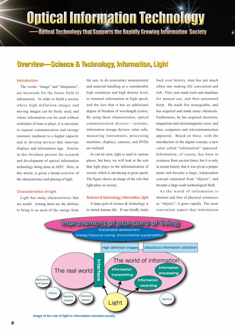
The figure shows an image of the role that
light plays in society.
Science & technology, information, lightA large goal of science & technology is
to enrich human life. If one briefly looks
back over history, man has put much
effort into making life convenient and
rich. First, man made tools and machines
for manual use, and then automated
them. He made fire manageable, and
has acquired and made many chemicals.
Furthermore, he has acquired electricity,
magnetism and electromagnetic wave, and
then, computers and telecommunication
appeared. Based on these, with the
introduction of the digital concept, a new
value called “information” appeared.
Information, of course, has been in
existence from ancient times, but it is only
in recent history that it was given a proper
name and became a large, independent
concept separated from “objects”, and
became a large-scale technological field.
As the wor ld o f in fo rma t ion i s
abstract and free of physical existences
as “objects”, it grew rapidly. The most
convenient aspect that information
2
Overview—Science & Technology, Information, Light
Image of the role of light in information-oriented society
Sustainable development (energy/resource saving, environmental sustainability)
The world of information
The real world
Light
Information
transmitting
Information
processing
Information
recording
High definition images Ubiquitous information utilization
Interface
Improvement of standard of living
Agriculture and forestry
FisheryMachineindustry
Chemical industry Electron
光情報技術−急成長する情報化時代を支える光技術
3
光情報技術−急成長する情報化時代を支える光技術
DirectorPhotonics Research Institute
Masanobu Watanabe
technology brings about is that new data
can easily be produced and processed (data
processing), stored (recording), and be
carried far at high speed (transmission).
The fundamental technologies of the
field of information are these three. In
addition to these, in order for man to use
information, technology that functions
as in terface between the world of
information and the real world through an
“object” medium is needed.
Optical technology is an important basic
technology that supports an information-
oriented society which is expected to grow
rapidly, and of the four aspects, it executes
strength in transmission, recording and
interface. This is demonstrated in optical
communication which transmits large
quantity of data at high speed, in optical
disks which can store large quantity of
data compactly and which are portable,
and in cameras and displays which can
acquire and show high definition images.
Let us look at one example. An
important aspect of informatization in
recent years has been the development of
the Internet, and, in these few years, the
amount of data flow has increased rapidly
at an annual rate of over 40 %. The
reasons for this are the increase of image
data, the move toward higher definition
and the increase in moving images,
and this tendency is going to accelerate
in the future. The biggest channel by
which man acquires information is
through the eye, and to be able to freely
use image data which appeals to the
eye will greatly change the activities of
mankind. If technologies for processing,
recording, transmitting, and displaying
high definition images, moving images,
and 3D images are realized, and if the
images attain a high level of realistic
sensation as if one is actually there, then
TV conferences, remote medical care
and remote education will definitely
become usable. If this level is achieved,
then it will expand the virtual activities
of mankind. In order to realize this kind
of society, it is essential that massive
improvement is made in large capacity
optical communication and optical
recording, in high definition and large
screen displays, and in devices and
material technology.
Sustainable developmentAs the in f luences o f sc ience &
technology and industry that uses them
increase, and as the human activities
expand, there are growing concerns that
“sustainable development” may become
difficult. At AIST, we aim to solve this
problem and claim a basic principle
“to contribute to the realization of a
sustainable development of the society of
the earth by leading the steady industrial
technological innovation of our country”.
Formerly, we could make our lives better
by “consuming” resources and energy of
the earth, but from now on, we need to
restrain and dissolve the negative side as
well as make advancements at the same
time.
Information technology intrinsically
has the possibility of improving living
standards with low consumption, and can
contribute greatly to improving efficiency
in such hardware areas as machinery,
chemical, and manufacturing industries.
For example, a large part of experiments
and trial manufacturing before making
the final product, can be replaced with
computation. The reason for the slow
spread of TV conferences, remote medical
care and remote education is thought to
be the lack of a sense of reality. If we can
solve this by further enlarging the capacity
of communication and by realizing large
screen displays, it will greatly reduce the
movement of people. Optical technology
can contribute greatly to the development
of these areas.
Conclusion In this brochure, the research activities
for large capacity optical communication
and recording, and devices for flexible
d i s p l a y s b e i n g d o n e a t A I S T a r e
introduced. These technologies contribute
to the handl ing of high def ini t ion
images and moving images, ubiquitous
information utilization (free of time or
place), and saving energy and resources.
With information technology which
makes rapid advancements, there is
always the concern for changes that are
beyond human assessment or control.
There is a need to control and eliminate
the negative aspects as well as to develop
the technology. With all this in mind,
we wil l cont inue the research and
development of optical technology that
supports the progress of an information-
oriented society, and would like to
contribute to the sustainable development
of mankind.

44
The future of the increase of network communication
The Internet is an indispensable part of
our lives. The amount of communication
through the Internet is increasing at an
annual rate of 40 %. Can it continue to
increase forever? Fig. 1 shows the future
estimation of network communication
amount and power consumption of routers.
The black and red dots are based on
government survey data, and the actual
lines are extrapolated from the observed
annual increase rates. What can be seen
from the figure is that the total router
power consumption increases as the
communication volume increases, and it
took up about 1 % of the total electric power
supply in 2006. This means that to enable
100-times increase of communication load
in the future, the power consumption of
the router needs to become 100 % of the
total electric power supply. The router, of
course, will become more highly efficient
in the future, but nevertheless, the present
technology will face limit.
On the other hand, looking at the
transition of network related technology
as the cause of increase in communication
volume, one can see that the use of network
has moved from the telephone (voice)
to data communication, and is presently
shifting toward video contents (Fig. 2). It is
thought that super high-definition imaging
technology such as super hi-vision[1] will
be widely used in the future. Then, the
concept of “remote co-existence” through
the network will become possible, and
most of the activities that were done by
meeting in person will be able to be done at
a distance. For example, 24 hour sharing of
space information through a screen which
occupies the entire wall of a living room
will make “distant living together” situation
become technologically feasible.
Optical path network expected to increase energy efficiency by several digits
We need to create a network technology
that can handle volumes larger by several
digits with which we can easily exchange
high definition videos, without increasing
energy consumption. Looking at Fig. 2,
one can see that the granularity per user (unit
of data volume processed by a user through
the network) is changing from digital packet
to optical fiber line (or optical fiber path).
Keeping this in mind, we are focusing on
optical path network or an optical circuit
switching system which switches optical
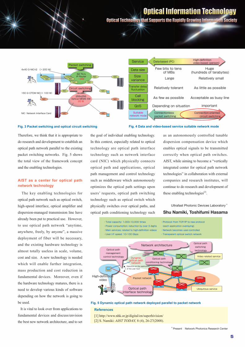
fibers/paths. As can be seen in Fig. 3,
compared to existing packet switching, if
only considering node processing, optical
path network which switches optical fibers/
paths with optical switches can save energy
by 3, 4 digits.
There is no other low-power technology
that is as simple and that has large potential
as this. However, optical path network
is not a packet switching network as the
existing one but a circuit switching one.
Fig. 4 shows the difference between data
transfer between computers, and transfer
of a live image of a person. Simply said,
packet switching is suitable for the former,
whereas circuit switching is suitable for
the latter. As the network handles both
data and videos, the packet switching and
the circuit switching are complementary.
4
Concept of Optical Path Network
Fig. 1 The Internet communication volume and the increase of power consumption of the routers
Fig. 2 Transition of network services and related technologies
1,000,000
100,000
10,000
1,000
100
1
10
2000 203020202010 20502040
100,000
10,000
1,000
100
1
10
0.1
Annual pow
er consumption of
electronic routers (100 m
illion kWh)
3~4 digits reduction of power consumption needed
Almost all is large volume data transfer of high definition videos
Annual energy production (2005)
Total Internet communication
volum
e (Tbps)
Increa
se of
40 % per annum
Increas
e of
20 % p
er annu
m
Traffic
Power
consum
ption
Lowerin
g voltag
e
of elect
ronic ci
rcuit
(Year)
Band occupancy application
High-definition video resolution / band
Storage
Year
Traffic
Per userEthernet I/F
Access connectivity
Granularity per user
Type of network
Application view
pointNetw
ork viewpoint
EmailWWW
SD0.2 Gbps
CD700 MB
100BASE-T
Dial-up
Voice10 kbps
P2PYouTube
HDTV1.5 Gbps
10G-BASE-T
PON-FTTH
Sub-wavelength towavelegnth> 100 Mbps
NGN/ROADM
0.01 1 > 100
Digital packet Optical fiber path
Telephone
DVD9 GB
1990's 2020's2000's 2010's
ADSL/Cable
1000BASE-T
Twisted pair1-10 Mbps
Internet
IPTVTV conference/telephone
4 k20 Gbps
Blu-ray50 GB
Remote co-existence telepresence
8 k(SHV)72 Gbps
Multi-layered / near field optics?
> 1,000
100G?
Dedicatedconnections
Wavelength toFiber
> 10 Gbps
Dynamic optical path network
Data Video
5
光情報技術−急成長する情報化時代を支える光技術
Ultrafast Photonic Devices Laboratory*
Shu Namiki, Toshifumi Hasama
Therefore, we think that it is appropriate to
do research and development to establish an
optical path network parallel to the existing
packet switching networks. Fig. 5 shows
the total view of the framework concept
and the enabling technologies.
AIST as a center for optical path network technology
The key enabling technologies for
optical path network such as optical switch,
high-speed interface, optical amplifier and
dispersion-managed transmission line have
already been put to practical use. However,
to use optical path network “anytime,
anywhere, freely, by anyone”, a massive
deployment of fiber will be necessary,
and the existing hardware technology is
almost totally useless in scale, volume,
cost and size. A new technology is needed
which will enable further integration,
mass production and cost reduction in
fundamental devices. Moreover, even if
the hardware technology matures, there is a
need to develop various kinds of software
depending on how the network is going to
be used.
It is vital to look over from applications to
fundamental devices and discuss/envision
the best new network architecture, and to set
the goal of individual enabling technology.
In this context, especially related to optical
technology are optical path interface
technology such as network interface
card (NIC) which physically connects
optical path and applications, optical
path management and control technology
such as middleware which autonomously
optimizes the optical path settings upon
users’ requests, optical path switching
technology such as optical switch which
physically switches over optical paths, and
optical path conditioning technology such
as an autonomously controlled tunable
dispersion compensation device which
enables optical signals to be transmitted
correctly when optical path switches.
AIST, while aiming to become a “vertically
integrated center for optical path network
technologies” in collaboration with external
companies and research institutes, will
continue to do research and development of
these enabling technologies[2].
Fig. 3 Packet switching and optical circuit switching
References[1] http://www.nhk.or.jp/digital/en/superhivision/[2] S. Namiki: AIST TODAY, 8 (4), 26-27(2008).
Fig. 4 Data and video-based service suitable network mode
Fig. 5 Dynamic optical path network deployed parallel to packet network
NIC NICNIC NICNIC NICNIC NICNIC NIC
NIC NIC
NIC
NIC
NIC
NIC
NICNIC
4x40 G-NIC×2 (> 200 W)
160 G-OTDM NIC(< 100 W)
NIC : Network Interface Card
82 Tb/sIP Router~MW
256x256Optical MEMS SW
20 W
Packet switching
Circuit switching
Suitablenetwork mode
Connection-oriented circuit switching
Connectionless packet switching
Service
Size variance
Transfer delayfluctuation
Callblocking
QoS
As few as possible Acceptable as busy line
important
Relatively tolerant
Large
As little as possible
Relatively small
Huge (hundreds of terabytes)
High-definition video-based (person)Data-based (PC)
Depending on situation
Data size Few bits to tens of MBs
・ Protocol: from TCP/IP to new protocol
(each application overlaying)
・ Network becomes user-controlled
・ Transparent optical switch network
・ Total capacity: 1,000-10,000 times
・ Power consumption: reduction by over 3 digits
・ Main services: related to high-definition videos
・ User I/F speed: 10-100 Gbps
Video related service
Network architectureOptical path management
control technology Dynamicoptical pathnetwork
Selection on the application of the user host
Optical path interface technology
High-definition video Packet network
Ubiquitous service
Optical pathconditioning technology
Optical pathswitching technology
*Present Network Photonics Research Center
6
IntroductionIn recent years , the information
communication volume starting with the Internet
is increasing rapidly. There is an urgent need
for a photonic network which makes large
volume, high speed communication possible.
At present, to realize large volume optical
communication, efforts are made to increase the
number of channels, as well as to accelerate the
transmission speed per channel; however, when
the transmission speed exceeds 160 Gb/s (gigabit/
second) per channel, it is thought that, because
of the speed limitations of electronic devices, it
is difficult to continue using electric circuits to
process transmit-receive signals. Therefore, in
processing signals over 160 Gb/s, it is necessary
to process at ultra high speed without converting
light signals to electrical signals. To realize this,
the development of an ultrafast optical switch is
the key.
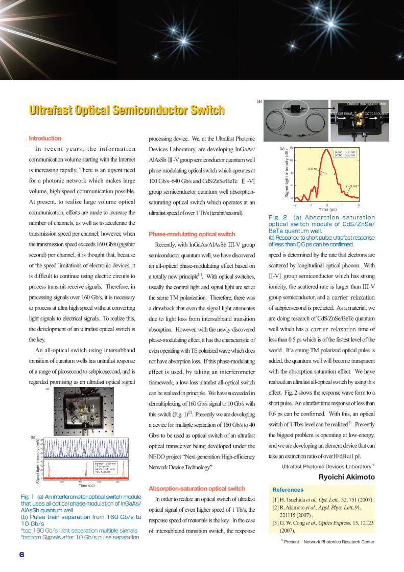
An all-optical switch using intersubband
transition of quantum wells has untrafast response
of a range of picosecond to subpicosecond, and is
regarded promising as an ultrafast optical signal
processing device. We, at the Ultrafast Photonic
Devices Laboratory, are developing InGaAs/
AlAsSb Ⅲ-V group semiconductor quantum well
phase-modulating optical switch which operates at
100 Gb/s~640 Gb/s and CdS/ZnSe/BeTe Ⅱ -VI group semiconductor quantum well absorption-
saturating optical switch which operates at an
ultrafast speed of over 1 Tb/s (terabit/second).
Phase-modulating optical switchRecently, with InGaAs/AlAsSb III-V group
semiconductor quantum well, we have discovered
an all-optical phase-modulating effect based on
a totally new principle[1]. With optical switches,
usually the control light and signal light are set at
the same TM polarization. Therefore, there was
a drawback that even the signal light attenuates
due to light loss from intersubband transition
absorption. However, with the newly discovered
phase-modulating effect, it has the characteristic of
even operating with TE polarized wave which does
not have absorption loss. If this phase-modulating
effect is used, by taking an interferometer
framework, a low-loss ultrafast all-optical switch
can be realized in principle. We have succeeded in
demultiplexing of 160 Gb/s signal to 10 Gb/s with
this switch (Fig. 1)[2]. Presently we are developing
a device for multiple separation of 160 Gb/s to 40
Gb/s to be used as optical switch of an ultrafast
optical transceiver being developed under the
NEDO project “Next-generation High-efficiency
Network Device Technology”.
Absorption-saturation optical switchIn order to realize an optical switch of ultrafast
optical signal of even higher speed of 1 Tb/s, the
response speed of materials is the key. In the case
of intersubband transition switch, the response
speed is determined by the rate that electrons are
scattered by longitudinal optical phonon. With
II-VI group semiconductor which has strong
ionicity, the scattered rate is larger than III-V
group semiconductor, and a carrier relaxation of subpicosecond is predicted. As a material, we
are doing research of CdS/ZnSe/BeTe quantum
well which has a carrier relaxation time of
less than 0.5 ps which is of the fastest level of the
world. If a strong TM polarized optical pulse is
added, the quantum well will become transparent
with the absorption saturation effect. We have
realized an ultrafast all-optical switch by using this
effect. Fig. 2 shows the response wave form to a
short pulse. An ultrafast time response of less than
0.6 ps can be confirmed. With this, an optical
switch of 1 Tb/s level can be realized[3]. Presently
the biggest problem is operating at low-energy,
and we are developing an element device that can
take an extinction ratio of over10 dB at1 pJ.
6
Ultrafast Optical Semiconductor Switch
References[1] H. Tsuchida et al., Opt. Lett., 32, 751 (2007) .[2] R. Akimoto et al., Appl. Phys. Lett.,91, 221115 (2007) .[3] G. W. Cong et al., Optics Express, 15, 12123 (2007).
Fig. 1 (a) An interferometer optical switch module that uses all-optical phase-modulation of InGaAs/AlAsSb quantum well(b) Pulse train separation from 160 Gb/s to 10 Gb/s *top 160 Gb/s light separation multiple signals*bottom Signals after 10 Gb/s pulse separation
Fig. 2 (a) Absorption saturation optical switch module of CdS/ZnSe/BeTe quantum well.(b) Response to short pulse; ultrafast response of less than 0.6 ps can be confirmed.
Ultrafast Photonic Devices Laboratory*
Ryoichi AkimotoTime (ps)
Signa
l light intens
ity (m
W)
300
(b)
control (1560 nm)=7 pJ/pulsesignal (1541 nm)=50 fJ/pulse
450400350
0
10
20
30
40
0
60
20
80
40
Optical input Optical output
Optical waveguide chip(a)
Time (ps)
Signal light intensity (dB)(b)
pump 1520 nmprobe 1566 nm
210-1-2
0
4
8
12
16
0.6 ps
τ~0.44
(a)
*Present Network Photonics Research Center
7
光情報技術−急成長する情報化時代を支える光技術
Optical Signal Processing Technology
Photonics Research Institute
Hidemi Tsuchida
IntroductionOptical communication technology is
expanding from a simple point-to-point
transmission to a network configuration that
contains a number of nodes (repeaters). A
network node fulfills such functions as path
switching, monitoring and regeneration
of signals, and gateway interconnecting
networks of d i fferent b i t ra te and
modulation format. These processes are
mainly performed using electronic circuits,
which causes problems concerning the
limitation of operating speed of electronic
devices, and the increase of energy
consumption resulting from the optical/
electrical/optical (O/E/O) conversion. In
order to efficiently distribute large volume
contents such as high-definition video, it
is necessary to construct a node that can
perform high-speed data signal processing
in the optical domain, without relying
on electronic circuits. Optical signal
processing is a basic technology to realize
such a network node, and a typical research
activity conducted at the Photonics
Research Institute is presented below.
Optical signal regeneration Since digital optical signals are degraded
during transmission and various processing
leading to bit errors at the receivers, there
is a need to regenerate the signals by
eliminating the various noise at the network
node. This type of signal processing is
called 3R regeneration (Re-amplification,
Re-timing, Re-shaping), and is currently
performed by electronic circuits, using an
equipment called transponder.
We have developed an optical 3R
regeneration technique that can process
optical data signals without relying on
O/E/O conversion. Fig. 1 shows the
schematic of the optical 3R regeneration
equipment. Re-amplification is performed
using the optical fiber amplifier. Re-timing
is a process that extracts reference clock
signals at the frequency corresponding
to the data signal bit rate by eliminating
modulation and noise components from
the incoming optical data signals. Then,
the extracted optical clock signals are
input to the ultrafast optical gate switch,
which performs waveform re-shaping
by switching the optical clock signals
according to the incoming optical data
signals. We have developed a regeneration
technique for 40-Gb/s optical data signals
by combining the optical clock extraction
using an injection-locked optoelectronic
oscillator and the semiconductor optical
amplifier-based optical gate switch. Fig.
2 shows the bit error rates of the optical
data signals obtained in the experiments.
Optical 3R regeneration is achieved with
a power penalty of 1.72 dB as compared
with the back-to-back operation. Also,
we confirmed operation at 160 Gb/s
using a similar equipment. For improving
the quality, stability and reliability of
regeneration, and for reducing the energy
consumption, it is necessary to enhance
the performance of each device such as
optical gate switches with hybrid integrated
configuration.
Future prospect The ultrafast optical signal processing
technology introduced here can treat digital
optical signals with on/off modulation of
optical pulses. Recently, new transmission
systems have been introduced that employ
advanced modulation format such as
phase and multi-level modulation. The
development of optical signal processing
technology for such complex modulation
format signals is strongly demanded in the
future, and we are planning to promote
research and development on this subject
in addition to ultrafast optical signal
processing.
Fig. 1 Schematic of optical 3R regeneration equipmentRegeneration of the optical data signals degraded during transmission and processing is performed through optical amplification, re-timing by optical clock extraction, and re-shaping by the optical gate switch.
Fig. 2 Bit error rate for 40-Gb/s optical 3R regeneration Error-free operation was achieved with the power penalty of 1.72 dB at the bit error rate of 10−9.
Degraded optical data signal Regenerated optical data signalOptical clock signal
Optical clock extraction
Optical gate switch
10
Optical amplification
Received optical power
Bit error rate Regenerated
Back-to-back
1.72 dB
-18 -12-13-14-15-16-17 -1110-12
10-10
10-8
10-4
10-2
10-6
8
Evolution and limit of optical discsOptical discs which started from CDs
have rapidly become popular in the progress
of information-oriented society, have
advanced from DVDs to Blu-ray discs, and
have continuously handled the explosive
increase of data volume (from sound to
images). Moreover, not only the ROM
(read only memory) discs but also the write-
once type and the rewriteable type discs
have been developed, and they have become
indispensable in our life.
In these optical discs, all information
has been digitalized. For example, digital
information is carved as a pit (minute
concave) in ROM discs. Therefore, the
increase of the recording capacity that led
from CD to DVD and to the Blu-ray discs
was achieved by improving the recording
density. The size of a minimum pit that is
870 nm in CD reduces to 400 nm in DVD,
and is reduced to 150 nm in Blu-ray discs.
The readout of the recorded information
is done exposing the pits with focused laser
beam and detecting the change of reflected
light intensity according to the presence or
absence of pits. Between the focus spot size
of laser light and the minimum readable pit
size, there is a limitation given of resolution
limit = 0.25 λ/NA (λ: wavelength of laser
light, NA: numerical aperture of lens). In other
words, spot size is defined by wavelength
and numerical aperture, and in order to
readout a smaller pit, a smaller spot is
needed. Therefore, 780 nm wavelength, NA
0.45 of optical system is used for CDs, 650
nm wavelength, NA 0.6 for DVDs, and 405
nm wavelength, NA 0.85 of optical system is
used for Blu-ray discs.
However, this improvement technique of
the capacity of data of these optical disc has
come to a limit. With the improvement of
fine processing technology, it has become
possible to make smaller pits of less than
100 nm, but the optical system is reaching
its limits. The numerical aperture is reaching
the physical limit (NA=1). Therefore, the
spot size reduction can only be done with
short wavelength. Optical components such
as lens and the material of the disc need to
be reviewed to use shorter wavelength, and
the development of a system that uses the
ultraviolet semiconductor laser is becoming
necessary. With optical discs of general use,
Blu-ray discs (resolution limit: 120 nm) are
said to be the limit of high density level in
the present system.
Presently, to respond to demands for
development of larger capacity optical discs
needed in advanced information-based
society, the constructing of new optical
memory systems (hologram and 2 photon
absorption memory) and the development of
technology that breaks the resolution limit
by using near-field light are needed. Here,
ultra high density disc called Super-RENS
which is being developed is presented as a
way to overcome the resolution limit and to
realize high density recording while using
the conventional system.
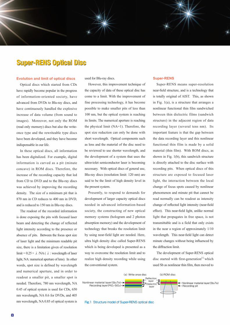
Super-RENSSuper-RENS means super-resolution
near-field structure, and is a technology that
is totally original of AIST. This, as shown
in Fig. 1(a), is a structure that arranges a
nonlinear functional thin film sandwiched
between thin dielectric films (sandwich
structure) in the adjacent region of data
recording layer (several tens nm). Its
important feature is that the gap between
the data recording layer and this nonlinear
functional thin film is made by a solid
material (thin film). With ROM discs, as
shown in Fig. 1(b), this sandwich structure
is directly attached to the disc surface with
recording pits. When optical discs of this
structure are exposed to focused laser
light, the interaction between the local
change of focus spots caused by nonlinear
phenomenon and minute pit that cannot be
read normally can be readout as intensity
change of reflected light intensity (near-field
effect). This near-field light, unlike normal
light that propagates in free space, is not
transmittable and is a field that only exists
in the near a region of approximately 1/10
wavelength. This near-field light can detect
minute changes without being influenced by
the diffraction limit.
The development of Super-RENS optical
disc started with first-generation[1] which
used Sb as nonlinear thin film, then moved to
8
Super-RENS Optical Disc
Fig.1 Structure model of Super-RENS optical disc
Reflectionlayer
Dielectriclayer
Nonlinear material layer(Sb₃Te)Recording layer(PtOx-SiO₂)
Write once disc
Nonlinear material layer(Sb₃Te)
ROM disc(b)(a)
Recording pit
9
光情報技術−急成長する情報化時代を支える光技術
Center for Applied Near-Field Optics Research
Takashi Nakano
second-generation[2] which used AgOx, and
has advanced to the present third generation[3]
which uses phase change material as
nonlinear layer. The nonlinear reactions of
these materials show high threshold level
against laser light intensity for readout, and
they react only at the laser focus spot. By
using the sandwich structure, the reactions
show reversibility. In order to realize a write
once optical disc, it is necessary to form
minute pits, and we have realized this by
using materials such as PtOx.[4, 5]
Characteristic of Super-RENS optical disc
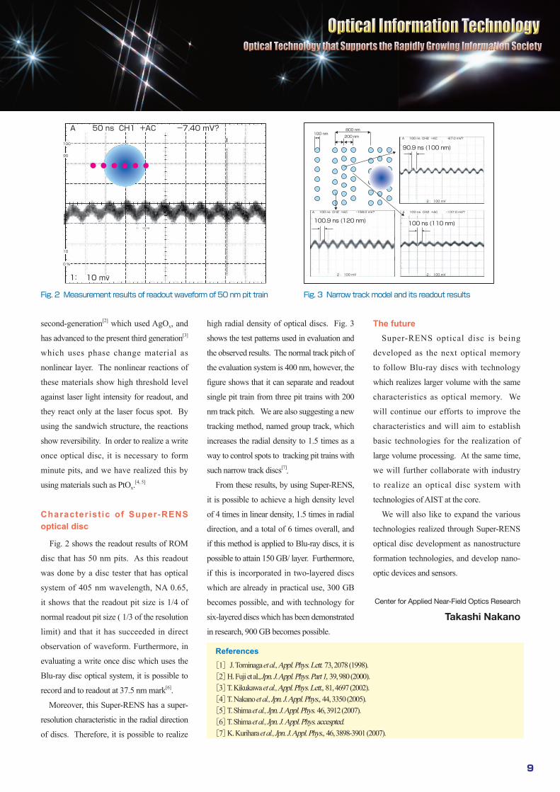
Fig. 2 shows the readout results of ROM
disc that has 50 nm pits. As this readout
was done by a disc tester that has optical
system of 405 nm wavelength, NA 0.65,
it shows that the readout pit size is 1/4 of
normal readout pit size ( 1/3 of the resolution
limit) and that it has succeeded in direct
observation of waveform. Furthermore, in
evaluating a write once disc which uses the
Blu-ray disc optical system, it is possible to
record and to readout at 37.5 nm mark[6].
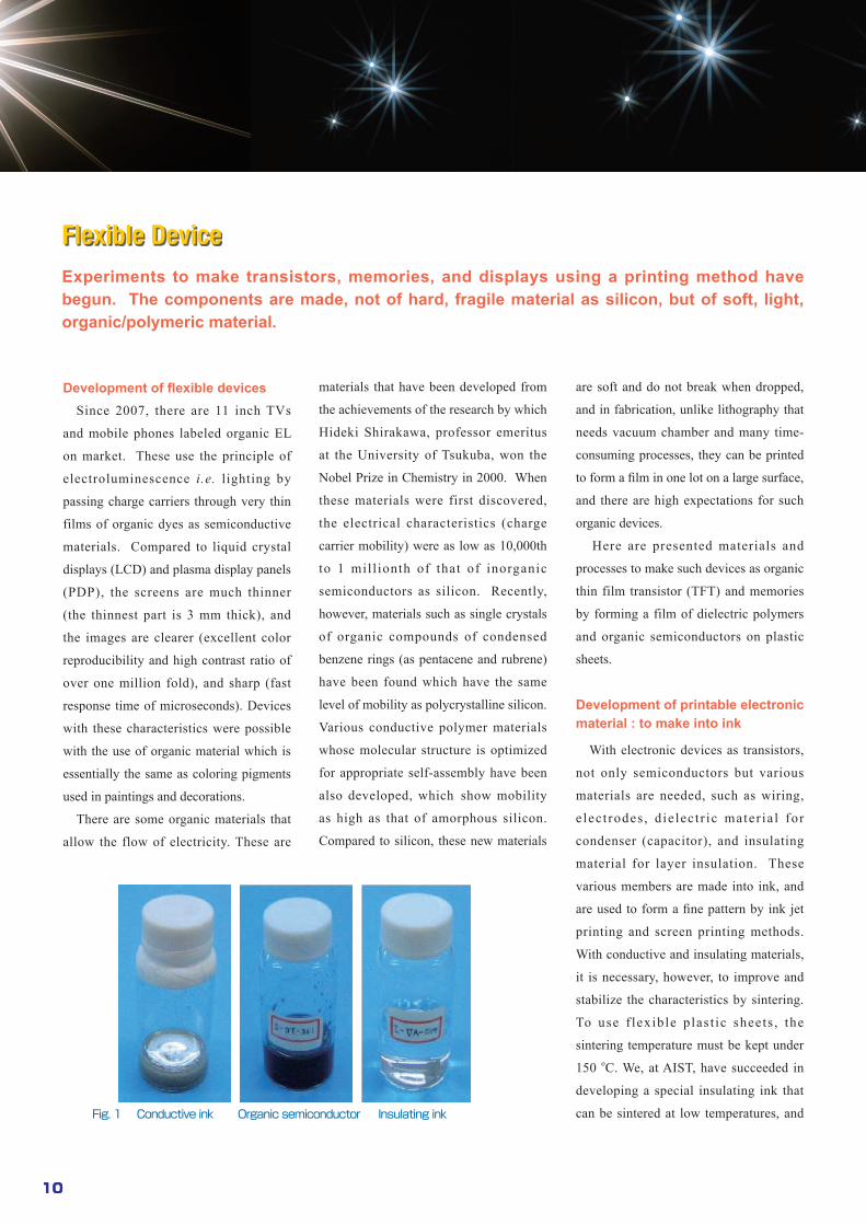
Moreover, this Super-RENS has a super-
resolution characteristic in the radial direction
of discs. Therefore, it is possible to realize
high radial density of optical discs. Fig. 3
shows the test patterns used in evaluation and
the observed results. The normal track pitch of
the evaluation system is 400 nm, however, the
figure shows that it can separate and readout
single pit train from three pit trains with 200
nm track pitch. We are also suggesting a new
tracking method, named group track, which
increases the radial density to 1.5 times as a
way to control spots to tracking pit trains with
such narrow track discs[7]. From these results, by using Super-RENS,
it is possible to achieve a high density level
of 4 times in linear density, 1.5 times in radial
direction, and a total of 6 times overall, and
if this method is applied to Blu-ray discs, it is
possible to attain 150 GB/ layer. Furthermore,
if this is incorporated in two-layered discs
which are already in practical use, 300 GB
becomes possible, and with technology for
six-layered discs which has been demonstrated
in research, 900 GB becomes possible.
The futureSuper-RENS optical disc is being
developed as the next optical memory
to follow Blu-ray discs with technology
which realizes larger volume with the same
characteristics as optical memory. We
will continue our efforts to improve the
characteristics and will aim to establish
basic technologies for the realization of
large volume processing. At the same time,
we will further collaborate with industry
to realize an optical disc system with
technologies of AIST at the core.
We will also like to expand the various
technologies realized through Super-RENS
optical disc development as nanostructure
formation technologies, and develop nano-
optic devices and sensors.
References
[1]J. Tominaga et al., Appl. Phys. Lett. 73, 2078 (1998).[2] H. Fuji et al., Jpn. J. Appl. Phys. Part 1, 39, 980 (2000).[3] T. Kikukawa et al., Appl. Phys. Lett., 81, 4697 (2002).[4] T. Nakano et al., Jpn. J. Appl. Phys., 44, 3350 (2005).[5] T. Shima et al., Jpn. J. Appl. Phys. 46, 3912 (2007).[6] T. Shima et al., Jpn. J. Appl. Phys. accespted.[7] K. Kurihara et al., Jpn. J. Appl. Phys., 46, 3898-3901 (2007).
Fig. 3 Narrow track model and its readout resultsFig. 2 Measurement results of readout waveform of 50 nm pit train
800 nm100 nm
200 nm
90.9 ns (100 nm)
100 ns (110 nm)100.9 ns (120 nm)
A 100 ns CH2 +AC -67.0 mV?
A 100 ns CH2 +AC -158.0 mV? A 100 ns CH2 +AC -137.0 mV?
2 : 100 mV
2 : 100 mV2 : 100 mV
A 50 ns CH1 +AC -7.40 mV?
1: 10 mv~
1: 10 mv~
100
90
10
0 %
10
Experiments to make transistors, memories, and displays using a printing method have begun. The components are made, not of hard, fragile material as silicon, but of soft, light, organic/polymeric material.
Development of flexible devicesSince 2007, there are 11 inch TVs
and mobile phones labeled organic EL
on market. These use the principle of
electroluminescence i.e. lighting by
passing charge carriers through very thin
films of organic dyes as semiconductive
materials. Compared to liquid crystal
displays (LCD) and plasma display panels
(PDP), the screens are much thinner
(the thinnest part is 3 mm thick), and
the images are clearer (excellent color
reproducibility and high contrast ratio of
over one million fold), and sharp (fast
response time of microseconds). Devices
with these characteristics were possible
with the use of organic material which is
essentially the same as coloring pigments
used in paintings and decorations.
There are some organic materials that
allow the flow of electricity. These are
materials that have been developed from
the achievements of the research by which
Hideki Shirakawa, professor emeritus
at the University of Tsukuba, won the
Nobel Prize in Chemistry in 2000. When
these materials were first discovered,
the electrical characteristics (charge
carrier mobility) were as low as 10,000th
to 1 mill ionth of that of inorganic
semiconductors as silicon. Recently,
however, materials such as single crystals
of organic compounds of condensed
benzene rings (as pentacene and rubrene)
have been found which have the same
level of mobility as polycrystalline silicon.
Various conductive polymer materials
whose molecular structure is optimized
for appropriate self-assembly have been
also developed, which show mobility
as high as that of amorphous silicon.
Compared to silicon, these new materials
10
are soft and do not break when dropped,
and in fabrication, unlike lithography that
needs vacuum chamber and many time-
consuming processes, they can be printed
to form a film in one lot on a large surface,
and there are high expectations for such
organic devices.
Here are presented materials and
processes to make such devices as organic
thin film transistor (TFT) and memories
by forming a film of dielectric polymers
and organic semiconductors on plastic
sheets.
Development of printable electronic material : to make into ink
With electronic devices as transistors,
not only semiconductors but various
materials are needed, such as wiring,
e lec t rodes , d ie lect r ic mater ia l for
condenser (capacitor), and insulating
material for layer insulation. These
various members are made into ink, and
are used to form a fine pattern by ink jet
printing and screen printing methods.
With conductive and insulating materials,
it is necessary, however, to improve and
stabilize the characteristics by sintering.
To use f lexible plast ic sheets , the
sintering temperature must be kept under
150 oC. We, at AIST, have succeeded in
developing a special insulating ink that
can be sintered at low temperatures, and Fig. 1 Conductive ink Organic semiconductor Insulating ink
Flexible Device
11
光情報技術−急成長する情報化時代を支える光技術
Photonics Research Institute
Kiyoshi Yase, Toshihide Kamata
also have successfully found a process to
form wire patterns in low temperatures
(Fig. 1).
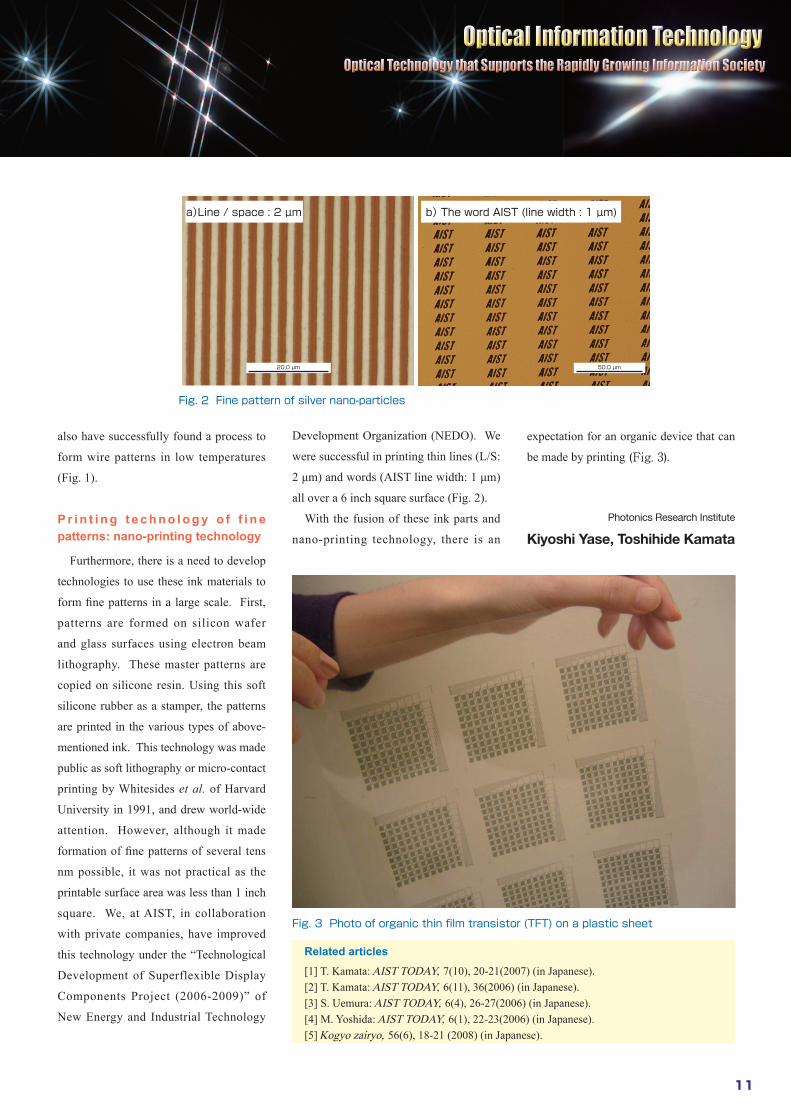
P r i n t i n g t e c h n o l o g y o f f i n e patterns: nano-printing technology
Furthermore, there is a need to develop
technologies to use these ink materials to
form fine patterns in a large scale. First,
patterns are formed on silicon wafer
and glass surfaces using electron beam
lithography. These master patterns are
copied on silicone resin. Using this soft
silicone rubber as a stamper, the patterns
are printed in the various types of above-
mentioned ink. This technology was made
public as soft lithography or micro-contact
printing by Whitesides et al. of Harvard
University in 1991, and drew world-wide
attention. However, although it made
formation of fine patterns of several tens
nm possible, it was not practical as the
printable surface area was less than 1 inch
square. We, at AIST, in collaboration
with private companies, have improved
this technology under the “Technological
Development of Superflexible Display
Components Project (2006-2009)” of
New Energy and Industrial Technology
Fig. 2 Fine pattern of silver nano-particles
Related articles[1] T. Kamata: AIST TODAY, 7(10), 20-21(2007) (in Japanese).[2] T. Kamata: AIST TODAY, 6(11), 36(2006) (in Japanese).[3] S. Uemura: AIST TODAY, 6(4), 26-27(2006) (in Japanese).[4] M. Yoshida: AIST TODAY, 6(1), 22-23(2006) (in Japanese).[5] Kogyo zairyo, 56(6), 18-21 (2008) (in Japanese).
Fig. 3 Photo of organic thin film transistor (TFT) on a plastic sheet
a)Line / space : 2 µm b) The word AIST (line width : 1 µm)
20.0 µm 50.0 µm
Development Organization (NEDO). We
were successful in printing thin lines (L/S:
2 μm) and words (AIST line width: 1 μm)
all over a 6 inch square surface (Fig. 2).
With the fusion of these ink parts and
nano-printing technology, there is an
expectation for an organic device that can
be made by printing (Fig. 3).
Optical Infoormation Technology Optical Technology that Supports the Rapidly Growing Information Society
Optical Information TechnologyOptical Technology that Supports the Rapidly Growing Information Society
● Overview—Science & Technology, Information, Light 2
Director, Photonics Research Institute
MasanobuWatanabe
● Concept of Optical Path Network 4 Ultrafast Photonic Devices Laboratory *
ShuNamiki,ToshifumiHasama
● Ultrafast Optical Semiconductor Switch 6 Ultrafast Photonic Devices Laboratory *
RyoichiAkimoto
● Optical Signal Processing Technology 7 Photonics Research Institute
HidemiTsuchida
● Super-RENS Optical Disc 8 Center for Applied Near-Field Optics Research
TakashiNakano
● Flexible Device 10 Photonics Research Institute
KiyoshiYase,ToshihideKamata
Publication Office, Public Relations Department, AIST AIST Tsukuba Central 2, 1-1-1 Umezono, Tsukuba, Ibaraki, 305-8568, JAPAN Tel:+81-29-862-6217 Fax:+81-29-862-6212 E-mail:[email protected] http://www.aist.go.jp/
The articles in this pamphlet were originally published in Japanese as the feature articles in the 2008-7 issue of AIST TODAY.Printed in Oct 2008
* Present : Network Photonics Research Center