NPT1012 Preliminary Datasheet Gallium Nitride 28V, … · NPT1012 Preliminary Datasheet ... • 4.0...
8
Jun. 2010 Page 1 NPT1012 Preliminary Datasheet This Preliminary Datasheet contains approximate product specifications which are representative of the product but are subject to change without notice. Package pin-out and mechanical dimensions are final. FEATURES • Optimized for broadband operation from DC-4000MHz • 25W P 3dB CW power at 3000MHz • 20-25W P 3dB CW power from 1000-2500MHz in application board with >50% drain efficiency • 12-20W P 3dB CW power from 30-1000MHz in ap- plication board with >50% drain efficiency • High efficiency from 14 - 28V • 4.0 °C/W R TH with maximum T J rating of 200 °C • Robust up to 10:1 VSWR mismatch at all angles with no device damage at 90 °C flange • Subject to EAR99 export control DC – 4000 MHz 25 Watt, 28 Volt GaN HEMT Gallium Nitride 28V, 25W RF Power Transistor Built using the SIGANTIC ® NRF1 process - A proprietary GaN-on-Silicon technology RF Specifications (CW, 3000MHz): V DS = 28V, I DQ = 225mA, T C = 25°C, Measured in Nitronex Test Fixture Symbol Parameter Min Typ Max Units P 3dB Average Output Power at 3dB Gain Compression 43 44 - dBm P 1dB Average Output Power at 1dB Gain Compression - 43 - dBm G SS Small Signal Gain 12 13 - dB h Drain Efficiency at 3dB Gain Compression 57 62 - % VSWR 10:1 VSWR at all phase angles No damage to the device Typical CW Performance in Figure 1 - Load-Pull, V DS = 28V, I DQ = 225mA Typical CW Performance Figure 2 - 1 over frequency in Load-Pull, V DS = 28V, I DQ = 225mA Note 1: 500MHz and 900MHz Load-Pull data collected using a 4.7 Ω resistor in the RF path added for stability
Transcript of NPT1012 Preliminary Datasheet Gallium Nitride 28V, … · NPT1012 Preliminary Datasheet ... • 4.0...
Jun. 2010Page 1
NPT1012 Preliminary Datasheet
This Preliminary Datasheet contains approximate product specifications which are representative of the product but are subject to change without notice. Package pin-out and mechanical dimensions are final.
FEATURES• Optimized for broadband operation from
DC-4000MHz• 25W P3dB CW power at 3000MHz• 20-25W P3dB CW power from 1000-2500MHz in
application board with >50% drain efficiency• 12-20W P3dB CW power from 30-1000MHz in ap-
plication board with >50% drain efficiency• High efficiency from 14 - 28V• 4.0 °C/W RTH with maximum TJ rating of 200 °C• Robust up to 10:1 VSWR mismatch at all angles
with no device damage at 90 °C flange• Subject to EAR99 export control
DC – 4000 MHz25 Watt, 28 Volt
GaN HEMT
Gallium Nitride 28V, 25W RF Power Transistor Built using the SIGANTIC® NRF1 process - A proprietary GaN-on-Silicon technology
RF Specifications (CW, 3000MHz): VDS = 28V, IDQ = 225mA, TC = 25°C, Measured in Nitronex Test Fixture
Symbol Parameter Min Typ Max Units
P3dB Average Output Power at 3dB Gain Compression 43 44 - dBm
P1dB Average Output Power at 1dB Gain Compression - 43 - dBmGSS Small Signal Gain 12 13 - dBh Drain Efficiency at 3dB Gain Compression 57 62 - %
VSWR 10:1 VSWR at all phase angles No damage to the device
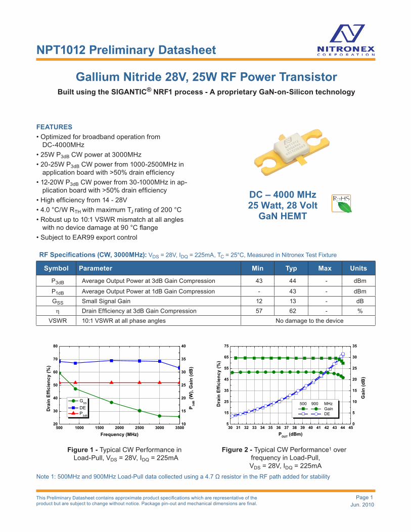
Typical CW Performance in Figure 1 - Load-Pull, VDS = 28V, IDQ = 225mA
Typical CW PerformanceFigure 2 - 1 over frequency in Load-Pull, VDS = 28V, IDQ = 225mA
Note 1: 500MHz and 900MHz Load-Pull data collected using a 4.7 Ω resistor in the RF path added for stability
Jun. 2010Page 2
NPT1012 Preliminary Datasheet
This Preliminary Datasheet contains approximate product specifications which are representative of the product but are subject to change without notice. Package pin-out and mechanical dimensions are final.
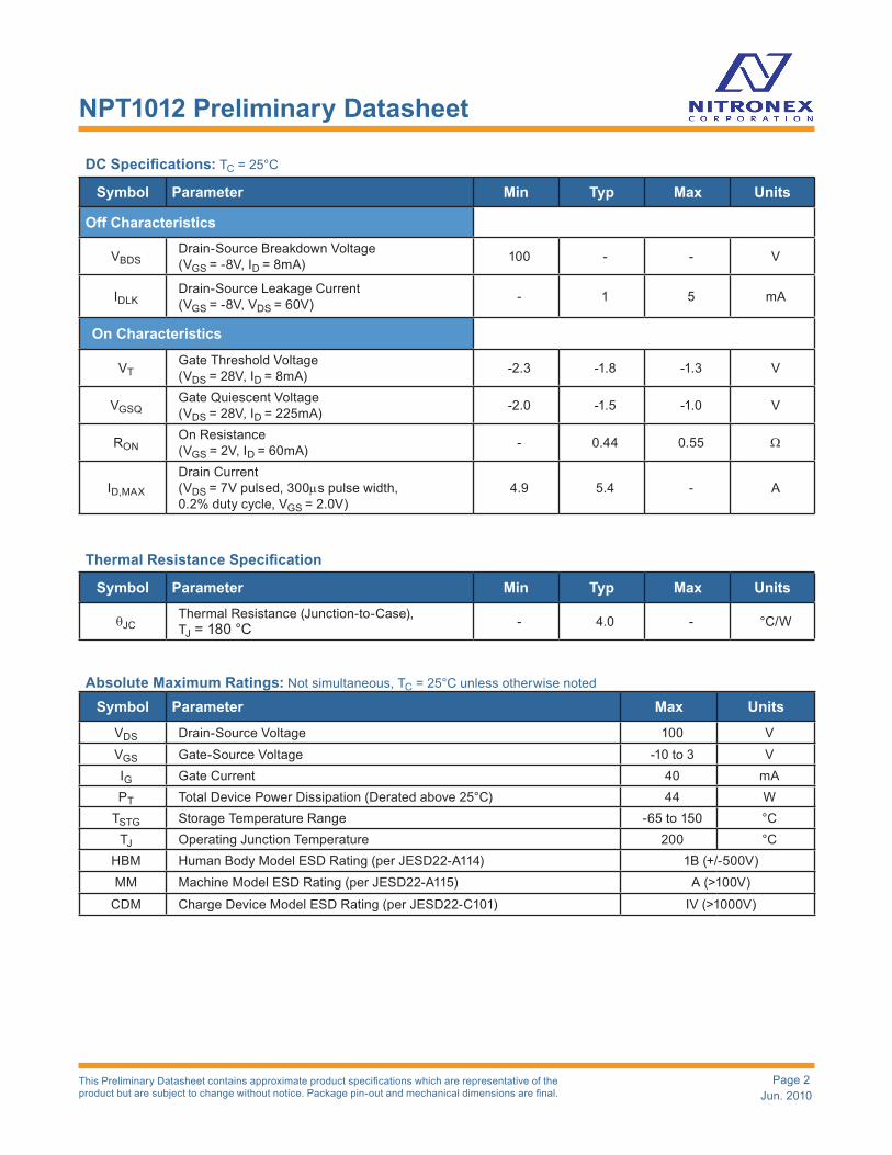
Absolute Maximum Ratings: Not simultaneous, TC = 25°C unless otherwise noted
Symbol Parameter Min Typ Max Units
Off Characteristics
VBDSDrain-Source Breakdown Voltage (VGS = -8V, ID = 8mA) 100 - - V
IDLKDrain-Source Leakage Current (VGS = -8V, VDS = 60V) - 1 5 mA
On Characteristics
VTGate Threshold Voltage (VDS = 28V, ID = 8mA) -2.3 -1.8 -1.3 V
VGSQGate Quiescent Voltage (VDS = 28V, ID = 225mA) -2.0 -1.5 -1.0 V
RONOn Resistance (VGS = 2V, ID = 60mA) - 0.44 0.55 W
ID,MAX
Drain Current (VDS = 7V pulsed, 300ms pulse width, 0.2% duty cycle, VGS = 2.0V)
4.9 5.4 - A
Symbol Parameter Max Units
VDS Drain-Source Voltage 100 VVGS Gate-Source Voltage -10 to 3 VIG Gate Current 40 mAPT Total Device Power Dissipation (Derated above 25°C) 44 W
TSTG Storage Temperature Range -65 to 150 °CTJ Operating Junction Temperature 200 °C
HBM Human Body Model ESD Rating (per JESD22-A114) 1B (+/-500V)MM Machine Model ESD Rating (per JESD22-A115) A (>100V)
CDM Charge Device Model ESD Rating (per JESD22-C101) IV (>1000V)
DC Specifications: TC = 25°C
Symbol Parameter Min Typ Max Units
qJCThermal Resistance (Junction-to-Case), TJ = 180 °C - 4.0 - °C/W
Thermal Resistance Specification
Jun. 2010Page 3
NPT1012 Preliminary Datasheet
This Preliminary Datasheet contains approximate product specifications which are representative of the product but are subject to change without notice. Package pin-out and mechanical dimensions are final.
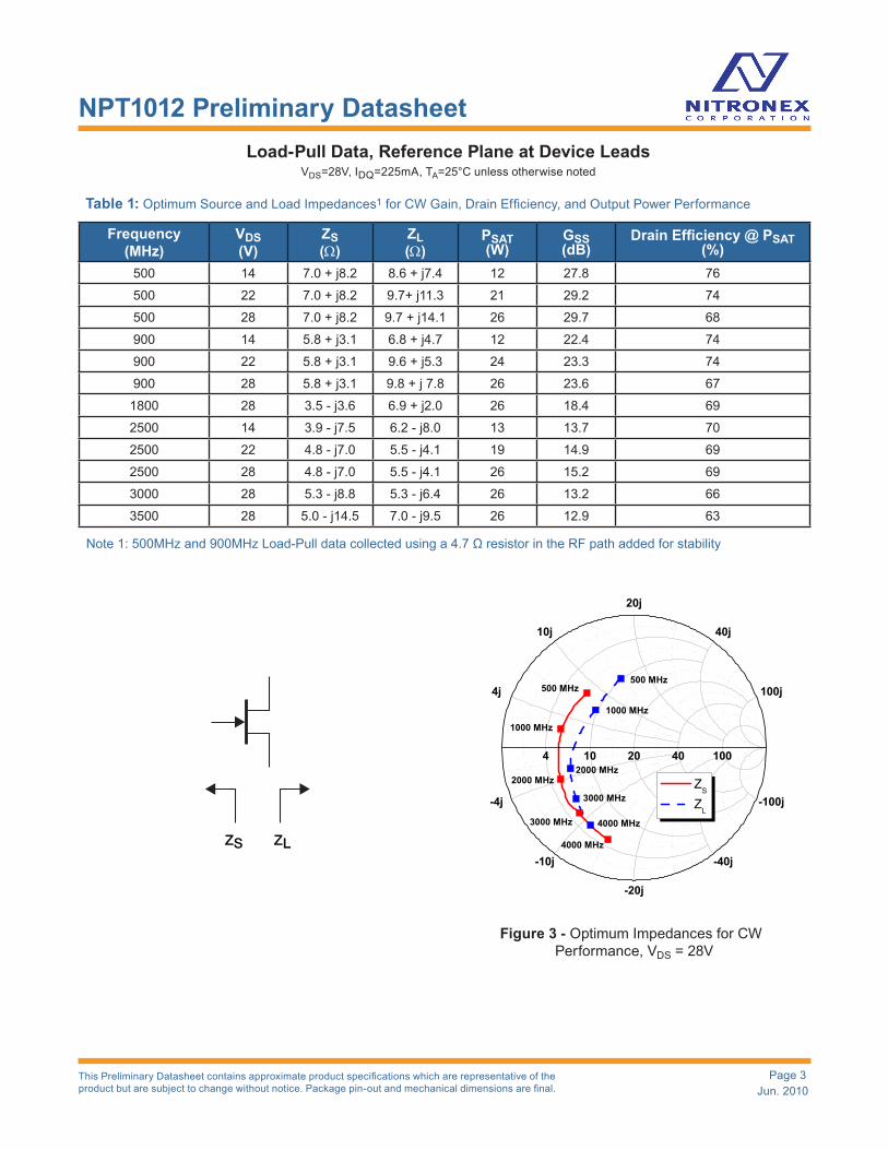
Table 1: Optimum Source and Load Impedances1 for CW Gain, Drain Efficiency, and Output Power Performance
Load-Pull Data, Reference Plane at Device LeadsVDS=28V, IDQ=225mA, TA=25°C unless otherwise noted
Optimum Impedances for CW Figure 3 - Performance, VDS = 28V
Frequency (MHz)
VDS (V)
ZS (W)
ZL (W)
PSAT (W)
GSS (dB)
Drain Efficiency @ PSAT (%)
500 14 7.0 + j8.2 8.6 + j7.4 12 27.8 76
500 22 7.0 + j8.2 9.7+ j11.3 21 29.2 74
500 28 7.0 + j8.2 9.7 + j14.1 26 29.7 68
900 14 5.8 + j3.1 6.8 + j4.7 12 22.4 74
900 22 5.8 + j3.1 9.6 + j5.3 24 23.3 74
900 28 5.8 + j3.1 9.8 + j 7.8 26 23.6 67
1800 28 3.5 - j3.6 6.9 + j2.0 26 18.4 69
2500 14 3.9 - j7.5 6.2 - j8.0 13 13.7 70
2500 22 4.8 - j7.0 5.5 - j4.1 19 14.9 69
2500 28 4.8 - j7.0 5.5 - j4.1 26 15.2 69
3000 28 5.3 - j8.8 5.3 - j6.4 26 13.2 66
3500 28 5.0 - j14.5 7.0 - j9.5 26 12.9 63
Note 1: 500MHz and 900MHz Load-Pull data collected using a 4.7 Ω resistor in the RF path added for stability
Jun. 2010Page 4
NPT1012 Preliminary Datasheet
This Preliminary Datasheet contains approximate product specifications which are representative of the product but are subject to change without notice. Package pin-out and mechanical dimensions are final.
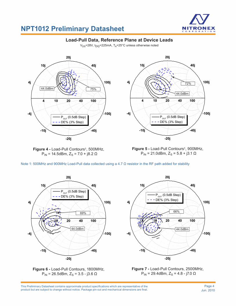
75%44.0dBm
Load-Pull ContoursFigure 4 - 1, 500MHz, PIN = 14.5dBm, ZS = 7.0 + j8.2 Ω
66%
44.0dBm
Note 1: 500MHz and 900MHz Load-Pull data collected using a 4.7 Ω resistor in the RF path added for stability
72%
44.0dBm
Load-Pull Data, Reference Plane at Device LeadsVDS=28V, IDQ=225mA, TA=25°C unless otherwise noted
69%
44.0dBm
Load-Pull ContoursFigure 5 - 1, 900MHz, PIN = 21.0dBm, ZS = 5.8 + j3.1 Ω
Load-Pull Contours, 1800MHz, Figure 6 - PIN = 26.5dBm, ZS = 3.5 - j3.6 Ω
Load-Pull Contours, 2500MHz, Figure 7 - PIN = 29.4dBm, ZS = 4.8 - j7.0 Ω
Jun. 2010Page 5
NPT1012 Preliminary Datasheet
This Preliminary Datasheet contains approximate product specifications which are representative of the product but are subject to change without notice. Package pin-out and mechanical dimensions are final.
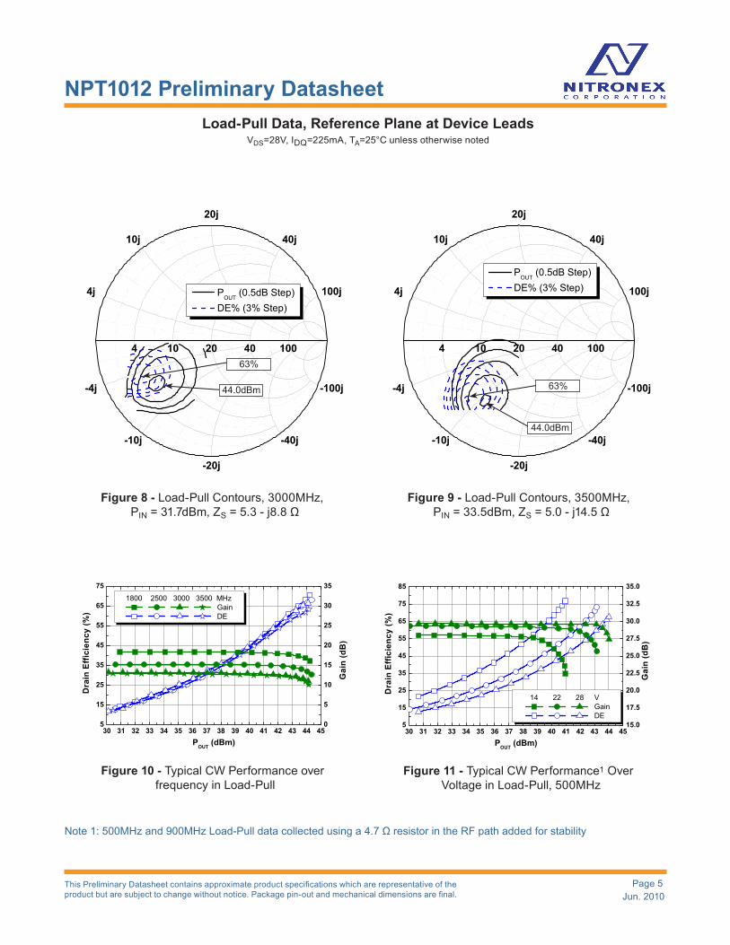
Load-Pull Data, Reference Plane at Device LeadsVDS=28V, IDQ=225mA, TA=25°C unless otherwise noted
63%
44.0dBm 63%
44.0dBm
Load-Pull Contours, 3000MHz, Figure 8 - PIN = 31.7dBm, ZS = 5.3 - j8.8 Ω
Load-Pull Contours, 3500MHz, Figure 9 - PIN = 33.5dBm, ZS = 5.0 - j14.5 Ω
Typical CW Performance over Figure 10 - frequency in Load-Pull
Typical CW PerformanceFigure 11 - 1 Over Voltage in Load-Pull, 500MHz
Note 1: 500MHz and 900MHz Load-Pull data collected using a 4.7 Ω resistor in the RF path added for stability
Jun. 2010Page 6
NPT1012 Preliminary Datasheet
This Preliminary Datasheet contains approximate product specifications which are representative of the product but are subject to change without notice. Package pin-out and mechanical dimensions are final.
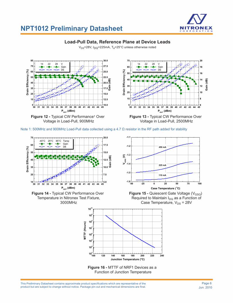
Typical CW PerformanceFigure 12 - 1 Over Voltage in Load-Pull, 900MHz
Typical CW Performance Over Figure 13 - Voltage in Load-Pull, 2500MHz
Typical CW Performance Over Figure 14 - Temperature in Nitronex Test Fixture,
3000MHz
Quiescent Gate Voltage (VFigure 15 - GSQ) Required to Maintain IDQ as a Function of
Case Temperature, VDS = 28V
MTTF of NRF1 Devices as a Figure 16 - Function of Junction Temperature
Note 1: 500MHz and 900MHz Load-Pull data collected using a 4.7 Ω resistor in the RF path added for stability
Load-Pull Data, Reference Plane at Device LeadsVDS=28V, IDQ=225mA, TA=25°C unless otherwise noted
Jun. 2010Page 7
NPT1012 Preliminary Datasheet
This Preliminary Datasheet contains approximate product specifications which are representative of the product but are subject to change without notice. Package pin-out and mechanical dimensions are final.
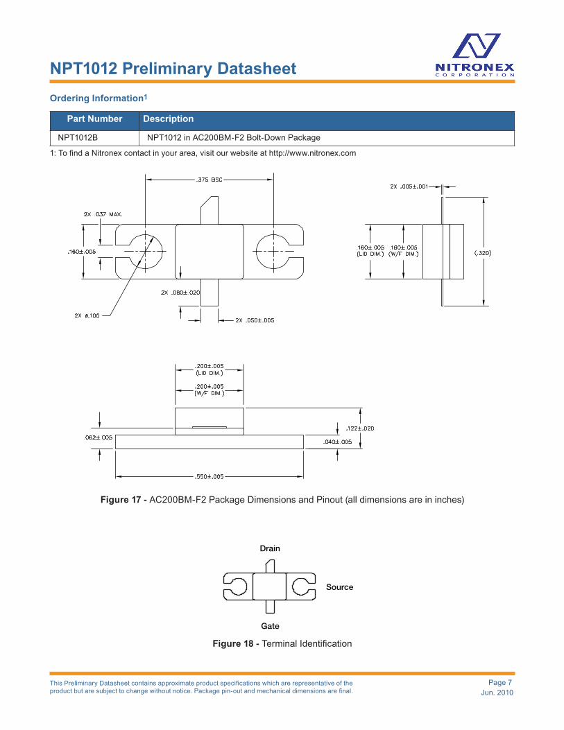
AC200BM-F2 Package Dimensions and Pinout (all dimensions are in inches)Figure 17 -
Terminal IdentificationFigure 18 -
Ordering Information1
Part Number Description
NPT1012B NPT1012 in AC200BM-F2 Bolt-Down Package
1: To find a Nitronex contact in your area, visit our website at http://www.nitronex.com
Drain
Gate
Source
Jun. 2010Page 8
NPT1012 Preliminary Datasheet
This Preliminary Datasheet contains approximate product specifications which are representative of the product but are subject to change without notice. Package pin-out and mechanical dimensions are final.
Nitronex Corporation2305 Presidential DriveDurham, NC 27703 USA+1.919.807.9100 (telephone)+1.919.807.9200 (fax)[email protected] www.nitronex.com
Additional InformationThis part is lead-free and is compliant with the RoHS directive (Restrictions on the Use of Certain Hazardous Substances in Electrical and Electronic Equipment).
Important NoticeNitronex Corporation reserves the right to make corrections, modifications, enhancements, improvements and other changes
to its products and services at any time and to discontinue any product or service without notice. Customers should obtain the latest relevant information before placing orders and should verify that such information is current and complete. All products are sold subject to Nitronex terms and conditions of sale supplied at the time of order acknowledgment. The latest information from Nitronex can be found either by calling Nitronex at 1-919-807-9100 or visiting our website at www.nitronex.com.
Nitronex warrants performance of its packaged semiconductor or die to the specifications applicable at the time of sale in accordance with Nitronex standard warranty. Testing and other quality control techniques are used to the extent Nitronex deems necessary to support the warranty. Except where mandated by government requirements, testing of all parameters of each product is not necessarily performed.
Nitronex assumes no liability for applications assistance or customer product design. Customers are responsible for their product and applications using Nitronex semiconductor products or services. To minimize the risks associated with customer products and applications, customers should provide adequate design and operating safeguards.
Nitronex does not warrant or represent that any license, either express or implied, is granted under any Nitronex patent right, copyright, mask work right, or other Nitronex intellectual property right relating to any combination, machine or process in which Nitronex products or services are used.
Reproduction of information in Nitronex data sheets is permitted if and only if said reproduction does not alter any of the information and is accompanied by all associated warranties, conditions, limitations and notices. Any alteration of the contained information invalidates all warranties and Nitronex is not responsible or liable for any such statements.
Nitronex products are not intended or authorized for use in life support systems, including but not limited to surgical implants into the body or any other application intended to support or sustain life. Should Buyer purchase or use Nitronex Corporation products for any such unintended or unauthorized application, Buyer shall indemnify and hold Nitronex Corporation, its officers, employees, subsidiaries, affiliates, distributors, and its successors harmless against all claims, costs, damages, and expenses, and reasonable attorney fees arising out of, directly or indirectly, any claim of personal injury or death associated with such unintended or unauthorized use, notwithstanding if such claim alleges that Nitronex was negligent regarding the design or manufacture of said products.
Nitronex and the Nitronex logo are registered trademarks of Nitronex Corporation.All other product or service names are the property of their respective owners.©Nitronex Corporation 2007. All rights reserved.