Notes Final Mid Hw Studio Quizes 4 1
83
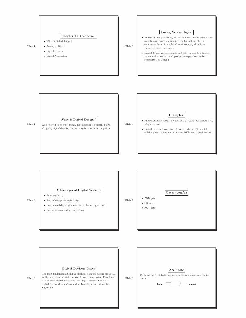
Slide 1 Chapter 1 Introduction • What is digital design ? • Analog v. Digital • Digital Devices • Digital Abstraction Slide 2 What is Digital Design ? Also referred to as logic design, digital design is concerned with designing digital circuits, devices or systems such as computers. Slide 3 Analog Versus Digital • Analog devices process signal that can assume any value across a continuous range and produce results that are also in continuous form. Examples of continuous signal include voltage, current, force, etc.. • Digital devices process signals that take on only two discrete values such as 0 and 1 and produces output that can be represented by 0 and 1. Slide 4 Examples • Analog Devices: solid-state devices TV (except for digital TV), telephone, etc. • Digital Devices: Computer, CD player, digital TV, digital cellular phone, electronic calculator, DVD, and digital camera. Slide 5 Advantages of Digital Systems • Reproducibility • Easy of design via logic design • Programmability-digital devices can be reprogrammed • Robust to noise and perturbations Slide 6 Digital Devices: Gates The most fundamental building blocks of a digital system are gates. A digital system (a chip) consists of many, many gates. They have one or more digital inputs and one digital output. Gates are digital devices that perform various basic logic operations. See Figure 1-1 Slide 7 Gates (cont’d) • AND gate • OR gate • NOT gate Slide 8 AND gate Performs the AND logic operation on its inputs and outputs its result. Input output
-
Upload
effectronfilms -
Category
Documents
-
view
457 -
download
2
description
COCO
Transcript of Notes Final Mid Hw Studio Quizes 4 1
Slide 1
Chapter 1 Introduction
• What is digital design ?
• Analog v. Digital
• Digital Devices
• Digital Abstraction
Slide 2
What is Digital Design ?
Also referred to as logic design, digital design is concerned with
designing digital circuits, devices or systems such as computers.
Slide 3
Analog Versus Digital
• Analog devices process signal that can assume any value across
a continuous range and produce results that are also in
continuous form. Examples of continuous signal include
voltage, current, force, etc..
• Digital devices process signals that take on only two discrete
values such as 0 and 1 and produces output that can be
represented by 0 and 1.
Slide 4
Examples
• Analog Devices: solid-state devices TV (except for digital TV),
telephone, etc.
• Digital Devices: Computer, CD player, digital TV, digital
cellular phone, electronic calculator, DVD, and digital camera.
Slide 5
Advantages of Digital Systems
• Reproducibility
• Easy of design via logic design
• Programmability-digital devices can be reprogrammed
• Robust to noise and perturbations
Slide 6
Digital Devices: Gates
The most fundamental building blocks of a digital system are gates.
A digital system (a chip) consists of many, many gates. They have
one or more digital inputs and one digital output. Gates are
digital devices that perform various basic logic operations. See
Figure 1-1
Slide 7
Gates (cont’d)
• AND gate
• OR gate
• NOT gate
Slide 8
AND gate
Performs the AND logic operation on its inputs and outputs its
result.
Input output

Slide 9
Characteristics of 2-Input AND gate
Four possible input combinations lead to two different outputs.
Slide 10
OR gate
Performs the OR logic operation on its inputs and outputs its
result.
Input output
Slide 11
Characteristics of 2-Input OR gate
Four possible input combinations lead to two different outputs.
Slide 12
NOT gate
Also referred to as inverter, produces an output value that is the
opposite of the input value.
Input output
Slide 13
Flip-Flop
A flip-flop (FF) is a device that stores a value of either 0 or 1. The
state (stored value) of a flip-flop depends on its current clock input.
Flip-flop can be constructed from gates. It is often used in
sequential circuit since it remembers. Memory is made up of FFs.
Slide 14
Digital Abstraction
Digital circuit deals with analog voltages and currents. Digital
abstraction allows analog behavior to be ignored. This can be
accomplished by associating a range of voltages with each logic
value. For example, the signals in a digital system might be
restricted to two levels -5 and + 5 volts, corresponding to two
discrete values of 0 and 1. It is necessary to understand the
operating environment (e.g., voltage, temperature, loading, ..)
under which the digital abstraction can be guaranteed.
Slide 15
Digital Abstraction
Alternatively, high and low are often used to represent 1 and 0
while discussing electronic logic.
Voltage Logic 1
Logic 0
High
Low
Logic 1
Logic 0
Invalid1.5 V
3,5 V
Outputs InputsMarginNoise
Slide 16
Software for Digital Design
Software is widely used in digital design. It can significantly reduce
design time, design cost, and improve design quality. It has been
mainly used for
• drawing schematic diagrams
• circuit simulation and modeling
• testing and debugging
• timing analysis
Software for simulation (e.g. LogicWorks) and programming
language (e.g. VHDL) for programming logic devices.
Slide 17
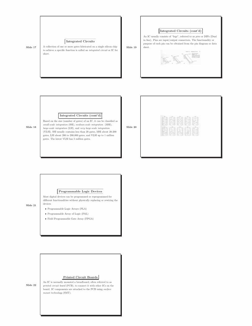
Integrated Circuits
A collection of one or more gates fabricated on a single silicon chip
to achieve a specific function is called an integrated circuit or IC for
short.
Slide 18
Integrated Circuits (cont’d)
Based on the size (number of gates) of an IC, it can be classified as
small-scale integration (SSI), medium-scale integration (MSI),
large-scale integration (LSI), and very large-scale integration
(VLSI). SSI usually contains less than 20 gates, MSI about 20-200
gates, LSI about 200 to 200,000 gates, and VLSI up to 1 million
gates. The latest VLSI has 5 million gates.
Slide 19
Integrated Circuits (cont’d)
An IC usually consists of “legs”, referred to as pins or DIPs (Dual
in line). Pins are input/output connectors. The functionality or
purpose of each pin can be obtained from the pin diagram or data
sheet.
Slide 20
Slide 21
Programmable Logic Devices
Most digital devices can be programmed or reprogrammed for
different functionalities without physically replacing or rewiring the
devices
• Programmable Logic Arrays (PLA)
• Programmable Array of Logic (PAL)
• Field Programmable Gate Array (FPGA)
Slide 22
Printed Circuit Boards
An IC is normally mounted a breadboard, often referred to as
printed circuit board (PCB), to connect it with other ICs on the
board. IC components are attached to the PCB using surface
mount technology (SMT).
Slide 1
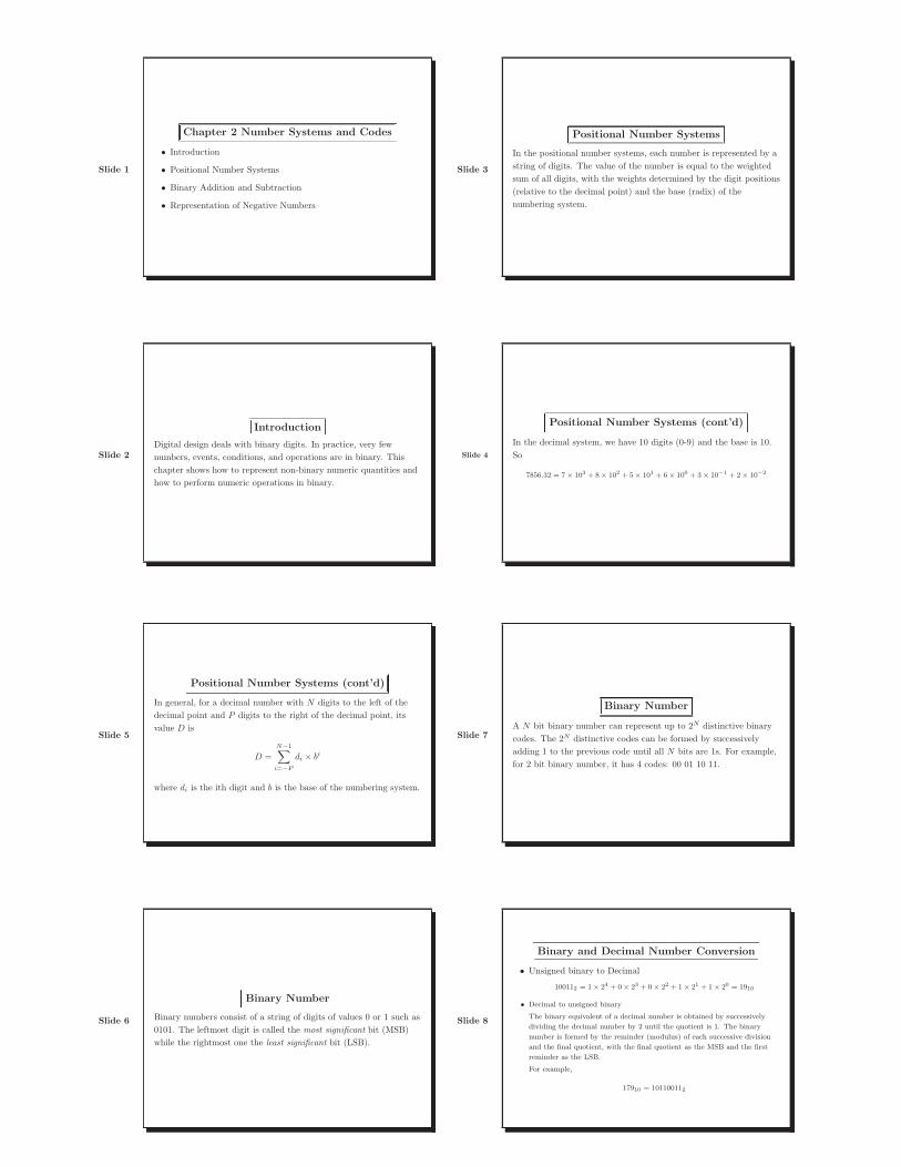
Chapter 2 Number Systems and Codes
• Introduction
• Positional Number Systems
• Binary Addition and Subtraction
• Representation of Negative Numbers
Slide 2
Introduction
Digital design deals with binary digits. In practice, very few
numbers, events, conditions, and operations are in binary. This
chapter shows how to represent non-binary numeric quantities and
how to perform numeric operations in binary.
Slide 3
Positional Number Systems
In the positional number systems, each number is represented by a
string of digits. The value of the number is equal to the weighted
sum of all digits, with the weights determined by the digit positions
(relative to the decimal point) and the base (radix) of the
numbering system.
Slide 4
Positional Number Systems (cont’d)
In the decimal system, we have 10 digits (0-9) and the base is 10.
So
7856.32 = 7× 10³ + 8× 10² + 5× 101 + 6× 100 + 3× 10⁻¹ + 2× 10⁻²
Slide 5
Positional Number Systems (cont’d)
In general, for a decimal number with N digits to the left of the
decimal point and P digits to the right of the decimal point, its
value D is
D =
N−1∑
i=−P
di × bi
where di is the ith digit and b is the base of the numbering system.
Slide 6
Binary Number
Binary numbers consist of a string of digits of values 0 or 1 such as
0101. The leftmost digit is called the most significant bit (MSB)
while the rightmost one the least significant bit (LSB).
Slide 7
Binary Number
A N bit binary number can represent up to 2N distinctive binary
codes. The 2N distinctive codes can be formed by successively
adding 1 to the previous code until all N bits are 1s. For example,
for 2 bit binary number, it has 4 codes: 00 01 10 11.
Slide 8
Binary and Decimal Number Conversion
• Unsigned binary to Decimal
100112 = 1× 24 + 0× 23 + 0× 22 + 1× 21 + 1× 20 = 1910
• Decimal to unsigned binary
The binary equivalent of a decimal number is obtained by successively
dividing the decimal number by 2 until the quotient is 1. The binary
number is formed by the reminder (modulus) of each successive division
and the final quotient, with the final quotient as the MSB and the first
reminder as the LSB.
For example,
17910 = 101100112

Slide 9
HEXADECIMAL Number
HEXADECIMAL number has a base of 16, consisting of 16 digits
ranging from 0 to 9 and A to F. For example, F1A3. Each hex digit
corresponds to 4 binary digits. The decimal value of a hex digit
ranges from 0 to 15.
Hex numbers are often used to describe computer memory location.
They are only used for human consumption.
Slide 10
HEX to DECIMAL
• HEX to Decimal
F1A316 = 15× 163 + 1× 162 + 10× 161 + 3× 160 = 6185910
• Decimal to HEX
The HEX equivalent of a decimal number may be obtained by successively
dividing the decimal number by 16 until the quotient is less than 16. The
HEX number is formed by the reminder of each successive division and the
final quotient, with the final quotient as the most significant digit (the left
most) and the first reminder as the least significant (the right most) digit.
For example,
341710 = D5916
Slide 11
HEX and Binary Conversion
• HEX to Binary: replace each HEX digit with four
corresponding binary digits as shown in Table 2-1.
F1A316 = 1111000110100011
• Binary to HEX: starting from right, replace each four binary digits with
the corresponding HEX digit as shown in Table 2-1. Add leading 0’s if
there are fewer than 4 bits.
Slide 12
For example,
011000110011102 = 18CE16
Refer to Table 2-2 for a summary of conversion methods.
Slide 13
Binary to Decimal
For a binary number of many digits, to convert it to decimal, it is
convenient to convert it to HEX first, and then from HEX to
decimal. Similarly, for a large decimal number, to convert it to
binary, it will be more efficient to convert it to HEX and then to
binary.
For example,
101110110012 = 5D916 = 5× 162 + 13× 161 + 9× 160 = 149710
Slide 14
OCTAL Numbers
The OCTAL numbering system has a base of 8, using digits 0-7.
Each OCTAL digit can be uniquely represented by 3 binary bits as
shown in Table 2-1.
Slide 15
OCTAL Numbers (cont’d)
OCTAL to decimal and the vice verse can be carried out the same
as HEX to decimal except for using base 8 instead of 16.
OCTAL to binary conversion can be accomplished the same way as
HEX to binary except that each OCTAL digit corresponds to 3
binary bit. While converting binary to OCTAL, starting from the
LSB and working towards left, separating binary bits into groups of
3 bits and replacing each group with the corresponding OCTAL
digit.
Octal to Hex (or vice verse) conversion needs to convert to binary
first, then to Hex,
Slide 16
Binary Addition and Subtraction
• Addition
• Subtraction
Slide 17
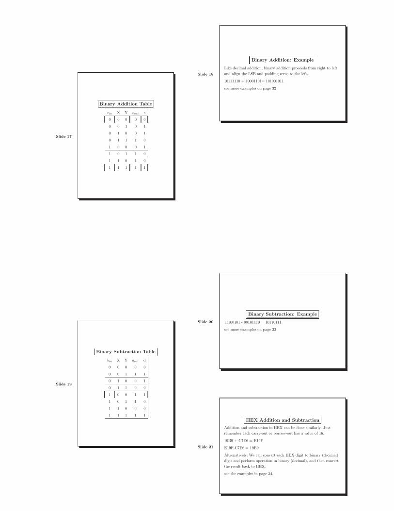
Binary Addition Table
cin X Y cout s
0 0 0 0 0
0 0 1 0 1
0 1 0 0 1
0 1 1 1 0
1 0 0 0 1
1 0 1 1 0
1 1 0 1 0
1 1 1 1 1
Slide 18
Binary Addition: Example
Like decimal addition, binary addition proceeds from right to left
and align the LSB and padding zeros to the left.
10111110 + 10001101= 101001011
see more examples on page 32
Slide 19
Binary Subtraction Table
bin X Y bout d
0 0 0 0 0
0 0 1 1 1
0 1 0 0 1
0 1 1 0 0
1 0 0 1 1
1 0 1 1 0
1 1 0 0 0
1 1 1 1 1
Slide 20
Binary Subtraction: Example
11100101 - 00101110 = 10110111
see more examples on page 33
Slide 21
HEX Addition and Subtraction
Addition and subtraction in HEX can be done similarly. Just
remember each carry-out or borrow-out has a value of 16.
19B9 + C7E6 = E19F
E19F-C7E6 = 19B9
Alternatively, We can convert each HEX digit to binary (decimal)
digit and perform operation in binary (decimal), and then convert
the result back to HEX.
see the examples in page 34.

Slide 22
Representation of Signed Numbers
• Signed Magnitude Representation
• Two’s Complement Representation
• Two’s Complement Addition and Subtraction
Slide 23
Signed Magnitude Representation
The MSB is the sign bit, with 0 for positive and 1 for negative
number. The decimal value of the number is determined only by
the remaining bits. Given n bits, the decimal value ranges from
−2n−1− 1 to 2n−1
− 1.
The major problem with this representation is that we have two
zeros: +0 and -0. It also has difficulty in performing addition and
subtraction.
Slide 24
Two’s Complement Representation
To represent a signed number in binary, we use two’s complement
binary system.
Slide 25
Two’s Complement Representation (cont’d)
According to the two’s complement representation, the MSB is the
sign bit. A number is positive if the MSB is zero or negative if
MSB is 1. The decimal value for a two’s complement binary
number is determined by all bits including the sign bit. The
decimal value is computed the same way as for an unsigned
number, except that the weight of the MSB is −2n−1. So in two’s
complement, binary and decimal conversion is
D =
n−1∑
i=0
di × 2i
, where di is -di for the MSB.
Slide 26
Two’s Complement Number Range
Like for unsigned binary, a N bit two’s complement number can
represent 2N decimal values ranging from −2n−1 to 2n−1− 1, one
extra negative number (−2n−1) that does not have its positive
counterpart.
Slide 27
Two’s Complementing
Two’s complementing is a binary operation. The two’s
complementing of a binary number is another binary number which
when added to the number yields zero if the MSB of the sum is
discarded
The two’s complementing of a binary number is obtained by
complementing each individual bit of the number and then add 1 to
the complemented number, ignoring the carry-out of the MSB. For
example, see page 37.
Slide 28
2’s Complement Representation v.2’s Complementing Operation
2’s complement representation is a binary representation scheme to
represent signed binary number while 2’s complementing operation
is a special type of complementing operation that applies only to
binary numbers represented in 2’s complement. The sum of a
binary number (represented in 2’s complement) and its 2’s
complement is 0.
For example,
1111 is a two’s complement representation of -1
The two’s complementing of 1111 is 0001, which represents +1.
So, 1111+0001=0000
Slide 29
Decimal to Two’s Complement
• Determine the number of bits needed to represent the decimal
number in two’s complement.
• for positive decimal number, proceed the same way as for
unsigned binary number, padding leading zeros if necessary.
• for negative decimal number, obtain two’s complement
representation for the corresponding positive number first,
followed by performing two’s complementing on the binary
number, yielding the two’s complement representation of the
negative number.
For example, for number 10, we need 5 bits, its two’s complement
is 01010. For -10, its two’s complement is obtained by two’s
complementing 01010, leading to 10110.

Slide 30
Two’s Complement Representation (cont’d)
Convert an n-bit two’s complement to a m-bit two’s complement, if
m > n, pad m− n copies of sign bit to the left of the number.
For example, to convert a 4-bit two’s complement number to a
8-bit complement number, pad 4 zeros.
0011 − > 00000011
1010 − > 11111010
If m < n, discard n−m leftmost bits and the result is valid only if
the discarded bits are the same as the sign bit.
8-bit to 4 bit
00000011 − > 0011
11111010 − > 1010
Slide 31
Two’s Complement Addition
Two’s complement addition can proceed the same as the unsigned
binary number addition, ignoring any carries beyond the MSB so
long as the sum remains within the range (no overflow).
see example on page 39
Slide 32
Two’s Complement Addition
Overflow occurs when the sum of two two’s complements exceeds
the range of the number system. An addition overflows if the signs
of the add-ends are the same and the sign of the sum is different
from the add-ends’ sign.
Another way to detect overflow is looking at the carry-in and
carry-out of the sign bit. Overflow occurs when the carry-in and
carry-out of the sign bit is different.
See examples on page 41. Note overflow may also occur if we
subtract two numbers of different signs.
Slide 33
Two’s Complement Subtraction
Two’s complement subtraction can be performed using the same
procedure as for the unsigned binary numbers. Like addition,
ignore the MSB borrows. Overflow may occur. It can be detected
by examining the borrow-in and borrow-out bit for the most
signifcant bit. For example,
over flow occurs for 0110-1101.
Alternatively, we can convert two’s complement subtraction into
two’s complement addition by converting subtrahend to its two’s
complement. See examples on page 42.
Slide 34
Other Issues
• Binary Code for Decimal (BCD)
• Gray code
• Character Codes
Slide 35
Binary Code for Decimal (BCD)
BCD encodes the digits 0 to 9 by the 4-bit unsigned binary
representation 0000 through 1001. The code words 1010 to 1111
are not used. see table 2.9. Packed-BCD allows to to place two
BCD digits in one byte, therefore representing values from 0-99.
Slide 36
Gray Code
Gray codes are binary numbers that have only one bit change
between successive code words. They may be used to represent
successive states or positions. On the other hand, the binary codes
of successive numbers may have more than one bit change between
successive codes. See 3-bit gray code in table 2-10.
Slide 37
Gray Codes Construction
Gray codes of any number of bits can be reconstructed recursively
using the three rules:
• A 1-bit gray code has two codes 0 and 1
• The first 2n−1 code words of an n-bit gray code equal the code
words of (n-1)-bit gray code, written in order with a leading
zero appended.
• The last 2n−1 code words of an n-bit gray code equal the code
words of (n-1)-bit gray code, but written in reverse order with
a leading 1 appended.
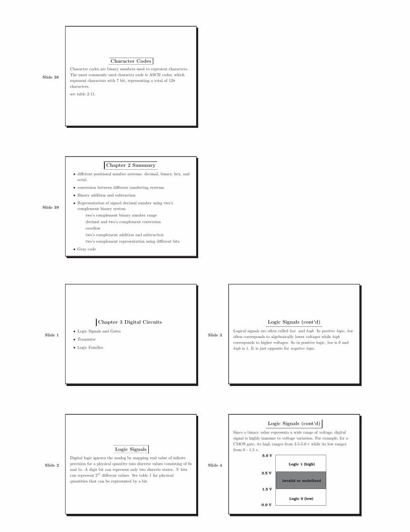
Slide 38
Character Codes
Character codes are binary numbers used to represent characters.
The most commonly used character code is ASCII codes, which
represent characters with 7 bit, representing a total of 128
characters.
see table 2-11.
Slide 39
Chapter 2 Summary
• different positional number systems: decimal, binary, hex, and
octal.
• conversion between different numbering systems.
• Binary addition and subtraction
• Representation of signed decimal number using two’s
complement binary system
two’s complement binary number range
decimal and two’s complement conversion
overflow
two’s complement addition and subtraction
two’s complement representation using different bits
• Gray code
Slide 1
Chapter 3 Digital Circuits
• Logic Signals and Gates
• Transistor
• Logic Families
Slide 2
Logic Signals
Digital logic ignores the analog by mapping real value of infinite
precision for a physical quantity into discrete values consisting of 0s
and 1s. A digit bit can represent only two discrete states. N bits
can represent 2N different values. See table 1 for physical
quantities that can be represented by a bit.
Slide 3
Logic Signals (cont’d)
Logical signals are often called low and high. In positive logic, low
often corresponds to algebraically lower voltages while high
corresponds to higher voltages. So in positive logic, low is 0 and
high is 1. It is just opposite for negative logic.
Slide 4
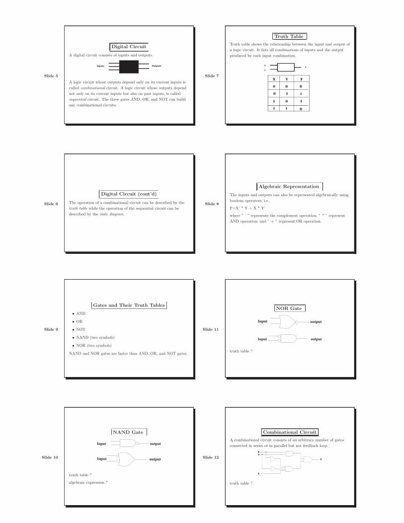
Logic Signals (cont’d)
Since a binary value represents a wide range of voltage, digital
signal is highly immune to voltage variation. For example, for a
CMOS gate, its high ranges from 3.5-5.0 v while its low ranges
from 0 - 1.5 v.
0.0 V
1.5 V
3.5 V
5.0 V
Logic 0 (low)
Logic 1 (high)
invalid or undefined
Slide 5
Digital Circuit
A digital circuit consists of inputs and outputs.
Inputs Outputs
A logic circuit whose outputs depend only on its current inputs is
called combinational circuit. A logic circuit whose outputs depend
not only on its current inputs but also on past inputs, is called
sequential circuit. The three gates AND, OR, and NOT can build
any combinational circuits.
Slide 6
Digital Circuit (cont’d)
The operation of a combinational circuit can be described by the
truth table while the operation of the sequential circuit can be
described by the state diagram.
Slide 7
Truth Table
Truth table shows the relationship between the input and output of
a logic circuit. It lists all combinations of inputs and the output
produced by each input combination.
Slide 8
Algebraic Representation
The inputs and outputs can also be represented algebraically using
boolean operators, i.e.,
F=X’ * Y + X * Y’
where ” ’ ” represents the complement operation, ” * ” represent
AND operation, and ” + ” represent OR operation.
Slide 9
Gates and Their Truth Tables
• AND
• OR
• NOT
• NAND (two symbols)
• NOR (two symbols)
NAND and NOR gates are faster than AND, OR, and NOT gates.
Slide 10
NAND Gate
Input output
Input output
truth table ?
algebraic expression ?
Slide 11
NOR Gate
Input output
Input output
truth table ?
Slide 12
Combinational Circuit
A combinational circuit consists of an arbitrary number of gates
connected in series or in parallel but not feedback loop.
XY
Z
F
truth table ?

Slide 13
Timing Diagram
Timing diagram is the dynamic representation of the truth table. It
represents input and output relationship as a function of the time.
X
Y
Z= X AND Y
Z
Note signals do not change between 0 and 1 instantaneously and
there is a transition period.
Slide 14
Transistor
see transistor.ppt
Slide 15
Logic Families
A logic family is a collection of different integrated circuit chips
that have similar input, output, and internal circuit characteristics,
but perform different logic functions. Chips from different families
may not be compatible. Each family is different in the technologies
used to produce the transistor.
Slide 16
Logic Families (cont’d)
Two most common logic families are Transistor-Transistor Logic
(TTL) and Complementary Metal-Oxide Semiconductor field effect
transistor (CMOS). They differ in materials, fabrication methods,
and electrical behaviors.
Slide 17
CMOS Logic
Section 3.3.2 - 3.3.4 introduce MOS transistors and the
construction of gates with MOS transistors.
Slide 18
Electrical Behavior of CMOS Circuits
The electrical behavior of a CMOS gate can be
characterized by the following electrical
properties:
• Logic voltage levels
• Noise margins
• Fan-in/Fan-out
• Speed (propagation delay)
• Power consumption

Slide 19
Logic Families (cont’d)
TTL gates are built on bipolar junction transistors while CMOS
are built on MOS transistors. They operate on different voltages.
For example, CMOS logic interprets 0-1.5 v as logic 0 and 3.5-5.0 v
as logic 1 while TTL logic interprets 0-0.8 v as logic 0 and 2.0-5.0 v
as logic 1.
By far, most integrated circuits use CMOS.
Slide 20
Noise Margin
��������������������������������
��������������������������������
��������������������������������������������
��������������������������������������������
���������������������������
���������������������������
������������������������������������������������
Inputsoutputs
voltage
logic 1
logic 0
logic 1
logic 0
invalid
NoiseMargin
Slide 21
Fan-in and Fan-out
Fan-in refers to the number of inputs a gate can have in a
particular logic family.
Fan-out refers to the maximum number of inputs that are
connected from the output of a gate. It depends not only on the
characteristics of the output, but also depends on the
characteristics of the input.
Slide 22
Fan-in
The number of inputs that a gate can practically have. Too many
inputs for a gate may lead to significant delay. The inputs to most
CMOS gates are limited to 4 to 6. Gates with a large number of
inputs can be made faster and efficient by cascading gates with
fewer inputs.
Slide 23
Fan-out
If too many fan-out are connected to an output, the DC noise
margin may not be adequate. Fanout may also affect speed.
Slide 24
Propagation Delay
There is a lag between an input change and the corresponding
output change. Propagation delay refers to the amount of time
needed for a change in the input signal to produce a change in the
output signal.
Slide 25
Data Sheets
The data sheet of a chip or a digital device
specifies the device’s logical and electrical
characteristics as well as operating conditions.
See table 3-3 for CMOS family and table 3-11 for
TTL family. To ensure the device work properly,
the operating conditions must be satisfied.
Slide 1
Chapter 4 Combinational Logic Design
This chapter is concerned with analysis and synthesis of
combinational logical circuit.
Analysis-start from a logic diagram of a circuit and proceed to a
formal description of the function of the circuit.
Synthesis-start with a formal description of the function of a
circuit and proceed to a logic diagram that performs the required
function.
Slide 2
Table of Contents
• Switching algebra (Boolean algebra)
• Circuit Analysis
• Circuit Synthesis
Slide 3
Switching Algebra
It is the mathematical foundation for logic design.
Notations:
’+’ stands for logic OR operation, e.g., x + y = x OR y
’·’ stands for logic AND operation, e.g, x · y = x AND Y
’′’ stands for logic NOT operation or complement, e.g., x′= NOT x
If a logic operation involves all the three operations, the precedence
order is: ′, ·, and +, e.g. , X + Y · Z ′.
Slide 4
Axioms
Axioms are a minimum set of basic mathematic definitions that we
assume to be always true and from which we can derive theorems.
Let X be a logic variable taking on values 0 or 1.
(A1) X=0 if X �= 1 (A1’) X=1 if X �= 0
(A2) If X=0, X ′ = 1 (A2’) If X=1, X ′ = 0
(A3) 0 · 0 =0 (A3’) 1 + 1 =1
(A4) 1 · 1 =1 (A4’) 0 + 0 =0
(A5) 0 · 1 =0 (A5’) 0 + 1 = 1+ 0=1
Slide 5
Single Variable Theorems
Let X be a logic variable
(T1) X + 0 = X (T1’) X · 1 = X
(T2) X + 1 = 1 (T2’) X · 0 = 0
(T3) X +X = X (T3’) X ·X = X
(T4) (X ′)′ = X
(T5) X +X ′ = 1 (T5’) X ·X ′ = 0
These theorems can be proved using axioms via perfect induction.
Slide 6
Two (Three) Variable Theorems
Let X , Y , Z be three logic variables
(T6) X + Y = Y +X (commuative)
(T6’) X · Y = Y ·X
(T7) (X + Y ) + Z = X + (Y + Z) (associative)
(T7’) (X · Y ) · Z = X · (Y · Z)
(T8) X · Y +X · Z = X · (Y + Z) (distributive)
(T8’) (X + Y ) · (X + Z) = X + Y · Z (note add out from right to
left)
(T9) X +X · Y = X (covering)
(T9’) X · (X + Y ) = X
(T10) X · Y +X · Y ′ = X (combining)
(T10’) (X + Y ) · (X + Y ′) = X
Slide 7
(T11) X · Y +X ′
· Z + Y · Z = X · Y +X ′
· Z (Consensus)
(T11’) (X + Y ) · (X ′ + Z) · (Y + Z) = (X + Y ) · (X ′ + Z)
In all the theorems, it is still true if a logic variable is replaced with
a logic expression.
Slide 8
Two (Three) Variable Theorems (cont’d)
Theorem T8 may be used to convert product of sums expression to
sum of products expression, for example
V · (W +X) · (Y +Z) = V ·W · Y + V ·W ·Z +V ·X · Y +V ·X ·Z
Theorem T8’ is often used to convert sum of products expression to
product of sums expression, for example
(V ·W · Z) + (Y · Z) = (V + Y ) · (W + Y ) · (Z + Y ) · Z
How about ((X + Y ′) · Z)) + (X ′
· Y · Z ′)
Proof of T8’ requires
X · (X+Y)= X + X · Y = X
Slide 9
Two (Three) Variable Theorems (cont’d)
Theorems 9, 10, and 11 are often used to minimize (simplify) a
logic circuit. They all share the property that there is a reduction
in the number of logic gates or the number of logic variables from
left to right.
Slide 10
n Variable Theorems
The two or three variables theorems can be extended to an
arbitrary number of variables, n as shown in table 4-3.
T12) X +X + ...+X = X
T12’) X ·X · ... ·X=X
The DeMorgan’s theorem (T13, T13’)
T13) (X1 ·X2 · ...Xn)′ = X ′
1+X ′
2+ ...+X ′
n
T13’) (X1 +X2 + ...+Xn)′ = (X ′
1·X ′
2· ...X ′
n)
see figure 4-3, 4-4 for the use DeMorgan’s theorem
The Generalized DeMorgan’s Law
T14) F ′(X1, X2, .., Xn,+, ·) = F (X ′
1, X ′
2, ....X ′
n, ·,+)
The generalized DeMorgan’s theorem (T14) states that given any
n-variable logic expression, its complement can be obtained by
Slide 11
swapping + and · and complementing all variables.
For example,
F (X,Y, Z) = X · Y + Z · Y
We have:
F′(X,Y, Z) = (X ′ + Y
′) · (Z ′ + Y′)
see more examples on page 192
Like theorem 8, DeMorgan’s law may be used to convert between
sum of products and product of sums.
Slide 12
Duality
Principle of Duality: Any theorem or logic equation remains true if
0 and 1 are swapped and · and + are swapped throughout. It
doubles the usefulness of everything.
In general, the dual of a logical expression F can be represented as
FD(X1, X2, . . . , Xn,+, ·, ′, 0, 1) = F (X1, X2, . . . , Xn, ·,+, ′, 1, 0)
where FD is the dual of F .
See previous theorems for example.
Slide 13
Duality v.s. DeMorgan’s Law
F′(X1, X2, . . . , Xn) = F
D(X ′
1, X
′
2, . . . , X
′
n)
See figures 4-7 and 4-8, where a type-1 gate is an AND gate if
positive logic is used or it is a OR gate, a type-2 gate is an OR gate
if positive logic is used or it is a AND gate. Simply, by changing
the logic convention, the two circuits produce the same output.
Slide 14
Duality v.s. DeMorgan’s Law
X2X3
X1
X4
X5
Xn
type 1
type 1
type 1
type 1
type 2
type 2
type 2
F(X1, X2, ... , Xn)
type 2
type 1
Copyright © 2000 by Prentice Hall, Inc. Digital Design Principles and Practices, 3/e
X2′X3′
X1′
X4′
X5′
Xn′
type 1
type 1
type 1
type 1
type 2
type 2
type 2
type 2
type 1 FD(X1′, X2′, ... , Xn′)
Copyright © 2000 by Prentice Hall, Inc. Digital Design Principles and Practices, 3/e
Slide 15
Logic Functions Representations
• Truth table, practical only for a small number of variables.
• Algebraic sum of minterms (Canonical Sum)
minterm : is a product of n distinctive logic variables (or their
complements), e.g., X · Y · Z.
the sum of minterms corresponds to the combination of
truth-table rows for which the function produces a 1 output.
Note for a n variable logic function, each minterm must consist
of n variables and within each minterm, each variable is
represented by its complement if the variable value is 0.
• Algebraic product of maxterms (Canonical Product)
maxterm : is the sum of n distinctive logic variables or their
complements, e.g., X+Y+Z
the product of maxterms corresponds to the product of
Slide 16
truth-table rows for which the function produces a 0 output.
Note for a n variable logic function, each maxterm must consist
of n variables and within each maxterm, each variable is
represented by its complement if the variable value is 1.
Slide 17
Algebraic representations
For the example in table 4-5 and 4-6, we have
Algebraic Sum of Minterms
F =∑
X,Y,Z
(0, 3, 4, 6, 7) = X′
· Y′
· Z′ +X
′
· Y · Z +
X · Y′
· Z′ +X · Y · Z
′ +X · Y · Z
Algebraic Product of MaxTerms
F =∏
X,Y,Z
(1, 2, 5) = (X + Y + Z′) · (X + Y
′ + Z) · (X ′ + Y + Z′)
Slide 18
Canonical Sum v. Canonical Product
To convert between canonical sum and canonical product, take the
set complement. For example,∑
A,B,C
(0, 1, 2, 3) =∏
A,B,C
(4, 5, 6, 7)
Note 1) both canonical sum and product are not minimal;2) sum
of products and product of sums may be minimal and each term
may not contain n variables.
Slide 19
An Example
• Given truth table, you should derive its canonical sum and
canonical product, and simplify the canonical expression.
• Given a logical expression, you should be able to
derive its truth table
canonical sum
canonical product
For example, given F=X+Y’Z’, derive its truth table, canonical
sum and canonical product.
Slide 20
Logic Combinational Circuit Analysis
Given the logic diagram of a circuit, obtain a formal description of
its logic function. From the logic function, we can determine
• circuit behaviors for various input combinations
• simplify (minimize) the circuit structure to obtain a different
circuit
• transform the algebraic description into standard form (e.g.,
sum of products or product of sums) for easy implementation.
Slide 21
Methods for Logic Function Description
• Truth table, good for small circuit but not practical for large
circuit with many inputs. From a truth table, we can directly
produce a logic expression in a standard form such as canonical
sum or product (sum of minterms or product of maxterms).
Alternatively, given a logic diagram, we can use a simulator to
automatically generate the output (or even the intermediate
results) for all possible input combinations.
Slide 22
• Algebraic expression
We can build an algebraic expression of a circuit by
propagating expressions from inputs through gates towards the
output. Boolean algebra may be used to simplify the expression
to obtain a different circuit of the same logic function.
Slide 23
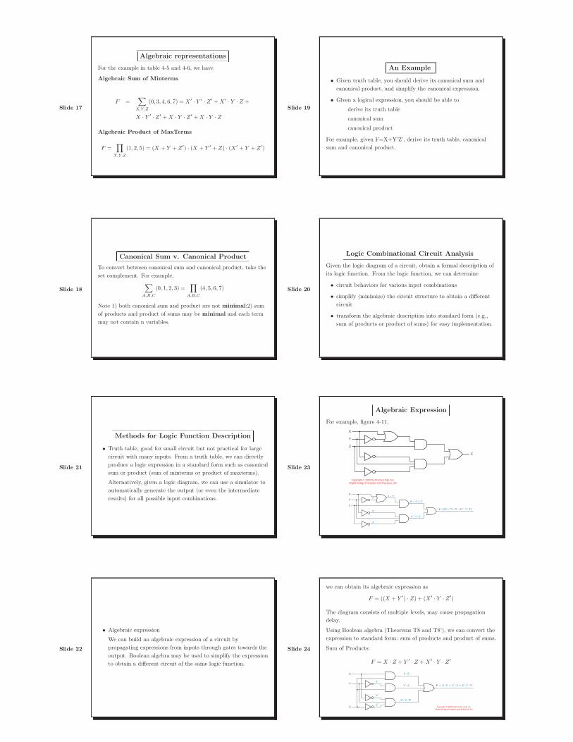
Algebraic Expression
For example, figure 4-11,
F
X
Y
Z
Copyright © 2000 by Prentice Hall, Inc. Digital Design Principles and Practices, 3/e
F
X
YY′
X + Y′
(X + Y′ ) • Z
X′
Z′
Z= ((X + Y′) • Z) + (X′ • Y • Z′)
X′ • Y • Z′
Slide 24
we can obtain its algebraic expression as
F = ((X + Y′) · Z) + (X ′
· Y · Z′)
The diagram consists of multiple levels, may cause propagation
delay.
Using Boolean algebra (Theorems T8 and T8’), we can convert the
expression to standard form: sum of products and product of sums.
Sum of Products:
F = X · Z + Y′
· Z +X′
· Y · Z′
F = X • Z + Y′ • Z + X′ • Y • Z′
X
Y
Z
Y′Y′ • Z
X • Z
X′ • Y • Z′
X′
Z′Copyright © 2000 by Prentice Hall, Inc.
Digital Design Principles and Practices, 3/e
Slide 25
Product of Sums:
F = (X + Y′ + Z
′) · (X ′ + Z) · (Y + Z)
X
YZ
Y′
Y + Z
X′ + Z
X + Y′ + Z′
X′
Z′
F = (X + Y′ + Z′) • (X′ + Z) • (Y + Z)
Copyright © 2000 by Prentice Hall, Inc. Digital Design Principles and Practices, 3/e
They correspond to different physical circuits (figures 4-12 and
4-13), each has only two levels.
Slide 26
Algebraic Expression (cont’d)
For circuits contains NAND and NOR gates, DeMorgan’s theorem
may be used to simplify the algebraic description of the circuit. See
example, 4-14 .
F
X
W
Y
Z
= [((W • X′)′ • Y)′ + (W′ + X + Y′)′+ (W + Z)′]′
X′(W • X′)′
((W • X′)′ • Y)′
(W′ + X + Y′)′
(W + Z)′
W′
Y′
Simply applying DeMorgan’s law yields an equivalent algebraic
expression.
F = ((W ′ +X) · Y )) · (W ′ +X + Y′) · (W + Z)
whose circuit is shown in Figure 4-16.
Slide 27
F
X
W
Y
Z
= ((W′ + X) • Y) • (W′ + X + Y′)• (W + Z)
X′W′ + X
((W′ + X) • Y)′
(W′ + X + Y′)′
(W + Z)′
W′
Y′
Given the same above expression, the circuit can be further
simplified by removing redundant NOT gates, leading to a different
physical circuit as shown in Figure 4-16.
F
X
W
Y
Z
= ((W′ + X) • Y) • (W′ + X + Y′)• (W + Z)
X′W′ + X
(W′ + X) • Y
W′ + X + Y′
W + Z
W′
Y′
Slide 28
Non-uniqueness in circuit representations
Normally, the algebraic logic expression may be ambiguous in that
it may correspond to different physical circuits depending on the
logic devices used. For example, in figure 4-17, one algebraic
expression
G=WXY+ YZ
corresponds to 3 different physical circuits.
WX
YZ
G
(a) (b)
(c)
WX
YZ
G
GWX
YZ
Y′
W • X • Y
W • X • Y
(W • X • Y)′
(W • X)′
(Y • Z)′Y • Z
Y • ZCopyright © 2000 by Prentice Hall, Inc.
Digital Design Principles and Practices, 3/e
Slide 29
They, though logically equivalent, may have different electrical
properties, costs, and sizes.
Slide 30
Logic Combinational Circuit Synthesis
• Given the informal (verbal) functional description of a circuit,
formalize the description with a truth table or an algebraic
expression and design a circuit based on the formal description
that performs the required logic function.
• Manipulate the algebraic expression to simplify (minimize) the
circuit.
Slide 31
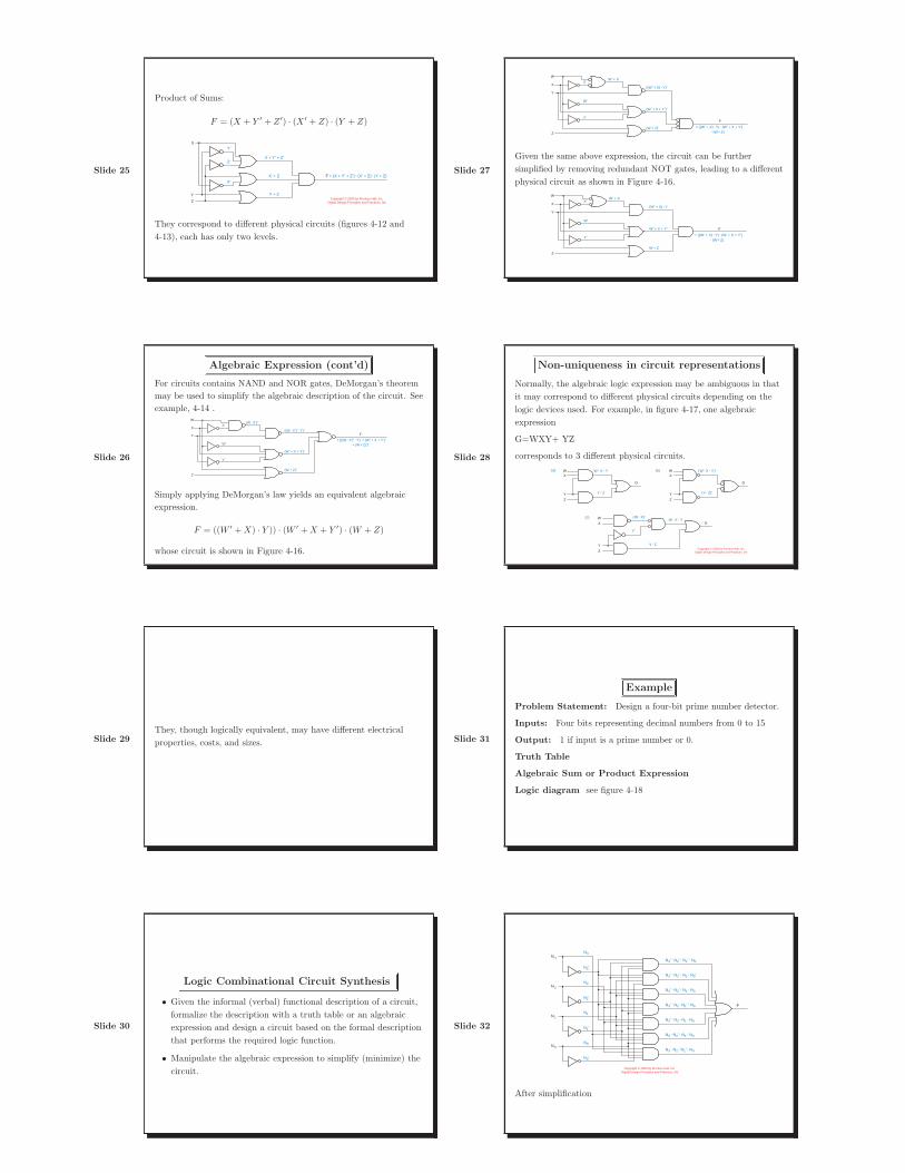
Example
Problem Statement: Design a four-bit prime number detector.
Inputs: Four bits representing decimal numbers from 0 to 15
Output: 1 if input is a prime number or 0.
Truth Table
Algebraic Sum or Product Expression
Logic diagram see figure 4-18
Slide 32
N 3
N3
N3′
N3′ • N2′ • N1′ • N0
N3′ • N2′ • N1 • N0′
N3′ • N2′ • N1 • N0
N3′ • N2 • N1′ • N0
N3′ • N2 • N1 • N0
N3 • N2′ • N1 • N0
N3 • N2 • N1′ • N0
N2
N2′
N1
N1′
N0
N0′
N 2
N 1
N 0
F
Copyright © 2000 by Prentice Hall, Inc. Digital Design Principles and Practices, 3/e
After simplification

Slide 33
N3
N2
N1
N0
F
N3 N3′ N2 N2′ N1 N1′ N0 N0′
N3′ • N0
N3′ • N2′ • N1 • N0′
N3 • N2′ • N1 • N0
N3 • N2 • N1′ • N0
Copyright © 2000 by Prentice Hall, Inc. Digital Design Principles and Practices, 3/e
Slide 34
Example (cont’d)
Also see the alarm example. Here, the functionality of a circuit is
described using logical connectives, which may be more convenient
than truth table.
Slide 35
Another Example
Design a two-bit odd number detector, which outputs one if the
input number is an odd number and 0 otherwise.
Slide 36
Circuit Manipulations
Given an algebraic representation of a logic circuit, we usually
manipulate the algebraic representation to
• convert it to standard forms
• replace with more efficient gates like NAND or NOR
• simplify (minimize) the expression
Slide 37
Convert to Standard Forms
Manipulate the expression using Boolean algebra (mostly theorems
T8 (multiply out), and T8’ (add out) and DeMorgan’s law) to
convert it to sum of products.
For example, figure 4-20 represents a sum-of-products version of
the original Boolean algebra. A two level logic diagram can be used
to represent a standard sum or product.
PANICALARM
ENABLE
EXITING
WINDOWDOOR
GARAGE
SECURECopyright © 2000 by Prentice Hall, Inc.
Digital Design Principles and Practices, 3/e
Slide 38
PANIC
ALARM
ENABLE
EXITING
WINDOW
DOOR
GARAGE
= PANIC+ ENABLE • EXITING′ • WINDOW′+ ENABLE • EXITING′ • DOOR′+ ENABLE • EXITING′ • GARAGE′
Copyright © 2000 by Prentice Hall, Inc. Digital Design Principles and Practices, 3/e
Slide 39
Use NAND and NOR gates
Since NAND and NOR are usually faster than AND, OR, and
NOT gates, they are often replaced with NAND and NOR gates.
For sum of products circuit, this can be achieved by inserting a pair
of inverters between the output of each AND gate and the input of
each OR gate. The inserted inverters can then be absorbed by the
AND and OR gates, leading to all NAND gates. For example, see
figures 4-21 and 4-22. We can conclude that any sum of products
circuit can be represented solely by NAND gates.
Slide 40
(c)
(a)(b)
Copyright © 2000 by Prentice Hall, Inc. Digital Design Principles and Practices, 3/e

Slide 41
Use NAND and NOR gates (cont’d)
For product of sums circuit, this can be achieved by inserting a pair
of inverters between the output of each OR gate and the input of
each AND gate. The inserted inverters can then be absorbed by
the OR and AND gates, leading to all NOR gates. For example, see
figure 4-23. We can conclude that any product of sums circuit can
be represented solely by NOR gates.
(a) (b)
(c)Copyright © 2000 by Prentice Hall, Inc. Digital Design Principles and Practices, 3/e
Slide 42
The same kind of manipulation can be applied to arbitrary logic
circuits as shown in Figure 4-24.
Slide 43
Combinational Circuit Minimization
Minimization means to reduce the number of gates of a circuit to a
minimal set that are needed to build the circuit.
Slide 44
Algebraic Minimization Procedure
• Start with truth table, sum of products or product of sums
expressions
For expressions not in a standard form, they need be converted
to one of the two standard forms before minimization.
• Apply theorems T9, T9’, T10, T10’ T11, and T11’.
see example in figure 4-25.
Slide 45
Graphical Approach: Karnaugh Map
Karnaugh Map is a graphical representation of the truth table. It
was invited by Maurice Karnaugh (a physicist) in 1953. More
details on the history of the K-map can be found at
http://en.wikipedia.org/wiki/Karnaugh map .
Slide 46
Karnaugh Map Construction
• label each column and row in the order of gray-code
• bracket each region where the corresponding variable is 1
• put the values of 1 or 0 in the corresponding cells, but not both.
Slide 47
Karnaugh Map Construction (cont’d)
• Two variable Karnaugh map
• Three variable Karnaugh map
• Four variable Karnaugh map
see figure 4-26 for example and understand the relationship
between the truth and the K-map.
Slide 48
Minimizing SOP with K-Map
The primary purpose of K-map is for minimization. We will show
how to use it to minimize algebraic representations in sum of
products (SOP).
• label each cell in K-map that corresponds to 1
• circle the adjacent 1-cells (minterms) and combine them
• write the sum of new products
Note
1) more than 2 1-cells may be combined
2) the number of cells in a circled region must be power of 2.
3) the circled region must be rectangular
4) account for all adjacent relationships
5) consider wrap-around when circling cells in the boundary

Slide 49
6) start with the region that includes the most number of 1-cells
see figure 4-27 for example.
Slide 50
Rule of Combination
Given a K-map with circled regions, the following rules specify how
to determine the form of the combined product graphically.
• If the circled area covers only regions where the variable is 0,
then the complement of the variable appears in the combined
form.
• If the circled area covers only regions where the variable is 1,
then the variable appears in the combined form.
• If the circled area covers both regions where the variable is 0
and 1, then the variable does not appear in the combined form.
see examples in figure 4-30, 4-31, and 4-32.
Slide 51
Minimal Sum
A minimum sum of products of a logic function is the one that has
the fewest possible number of product terms and that has
fewer or equal number of logic variables than any sum of
products expression of the same number of products.
Slide 52
Definitions
• a prime implicant in a K-map is a circled set of 1-cells that
satisfies combining rules and that will cover one or more 0s if
we make it larger
• a distinguished 1-cell is a 1-cell in a K-map that is covered
by only one prime implicant.
• an essential prime implicant is a prime implicant that
covers one or more distinguished cells.
• Given two prime implicants P and Q in a reduced K-map, P is
said to eclipse Q if P covers at least all the 1-cells covered by
Q.
Slide 53
Minimal Sum Theorem
A sum of essential prime implicants is always minimal. However, a
sum of prime implicants may not be minimal.
Slide 54
Procedure for Finding a Minimal Sum
• identify the essential prime implicants and include them in the
final sum.
• If the identified essential implicants cover all 1-cells, then done.
The resulting sum is minimal.
• If the identified essential implicants do not cover all 1-cells,
then remove the 1-cells covered by the essential prime
implicants, yielding a reduced map.
• In the reduced map, select the prime implicant a) that consists
of the fewest number of variables (see example in Figure 4-34);
or b) that eclipses other prime implicants (see example in
figure 4-35); c) select a minimum number of prime implicants
that cover all 1-cells.
Note the above procedure may not work for complex logic circuit.
Slide 55
In this case, trial and error may be used. For example, figure 4-37.
Programs (e.g. Espresso) are available that implement certain
algorithms to automatically find the minimal sum. See more
examples in problem 4-14. Also note the minimal sum may not be
unique.
Slide 56
Minimizing POS with Karnaugh Map
To minimize the product of sums, we can follow the same
procedure for sum of products except for circling and combining
regions corresponding to 0s. Note each circled region is represented
by a sum term. Within each sum term, a variable is represented by
itself if its value is 0 and by its complement if its value is 1.
The procedure for identifying the minimal sum remains applicable.
The prime implicants consist of circled zeros and look for
distinguished 0-cells for essential prime implicants.
Slide 57
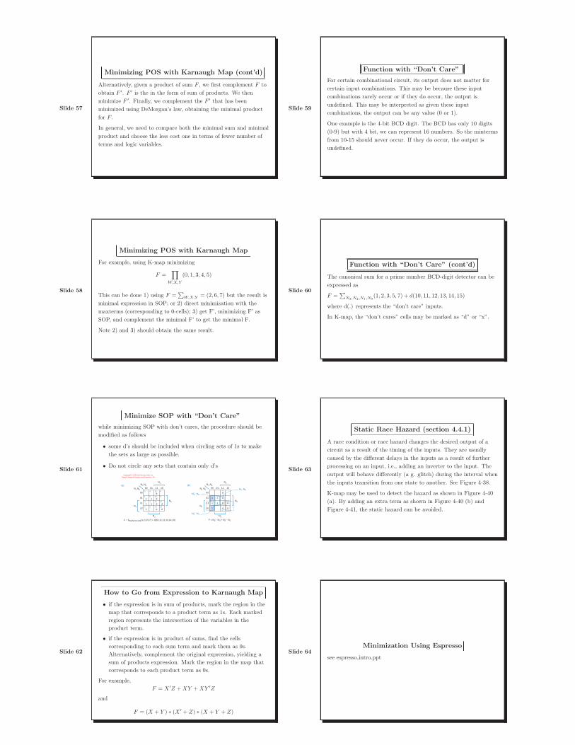
Minimizing POS with Karnaugh Map (cont’d)
Alternatively, given a product of sum F , we first complement F to
obtain F ′. F ′ is the in the form of sum of products. We then
minimize F ′. Finally, we complement the F ′ that has been
minimized using DeMorgan’s law, obtaining the minimal product
for F .
In general, we need to compare both the minimal sum and minimal
product and choose the less cost one in terms of fewer number of
terms and logic variables.
Slide 58
Minimizing POS with Karnaugh Map
For example, using K-map minimizing
F =∏
W,X,Y
(0, 1, 3, 4, 5)
This can be done 1) using F =∑
W,X,Y= (2, 6, 7) but the result is
minimal expression in SOP; or 2) direct minimization with the
maxterms (corresponding to 0-cells); 3) get F’, minimizing F’ as
SOP, and complement the minimal F’ to get the minimal F.
Note 2) and 3) should obtain the same result.
Slide 59
Function with “Don’t Care”
For certain combinational circuit, its output does not matter for
certain input combinations. This may be because these input
combinations rarely occur or if they do occur, the output is
undefined. This may be interpreted as given these input
combinations, the output can be any value (0 or 1).
One example is the 4-bit BCD digit. The BCD has only 10 digits
(0-9) but with 4 bit, we can represent 16 numbers. So the minterms
from 10-15 should never occur. If they do occur, the output is
undefined.
Slide 60
Function with “Don’t Care” (cont’d)
The canonical sum for a prime number BCD-digit detector can be
expressed as
F =∑
N3,N2,N1,N0(1, 2, 3, 5, 7) + d(10, 11, 12, 13, 14, 15)
where d(.) represents the “don’t care” inputs.
In K-map, the “don’t cares” cells may be marked as “d” or “x”.
Slide 61
Minimize SOP with “Don’t Care”
while minimizing SOP with don’t cares, the procedure should be
modified as follows
• some d’s should be included when circling sets of 1s to make
the sets as large as possible.
• Do not circle any sets that contain only d’s
0
1
3
2
4
5
7
6
12
13
15
14
8
9
11
10
00 01 11 10N3 N2
N1 N0
00
1 1 d
d
d
d
d
d
11
1
01
11
10
N3
N2
N1
N0
N3 N2
N1 N0
N3
N2
N1
N0
(a)00 01 11 10
00
1 1 d
d
d
d
d
d
11
1
01
(b)
F = N3′ • N0 + N2′ • N1
11
10
N3′ • N0
N2′ • N1
N2 • N0
F = ΣN3,N2,N1,N0(1,2,3,5,7) + d(10,11,12,13,14,15)
Copyright © 2000 by Prentice Hall, Inc. Digital Design Principles and Practices, 3/e
Slide 62
How to Go from Expression to Karnaugh Map
• if the expression is in sum of products, mark the region in the
map that corresponds to a product term as 1s. Each marked
region represents the intersection of the variables in the
product term.
• if the expression is in product of sums, find the cells
corresponding to each sum term and mark them as 0s.
Alternatively, complement the original expression, yielding a
sum of products expression. Mark the region in the map that
corresponds to each product term as 0s.
For example,
F = X′
Z +XY +XY′
Z
and
F = (X + Y ) ∗ (X ′ + Z) ∗ (X + Y + Z)
Slide 63
Static Race Hazard (section 4.4.1)
A race condition or race hazard changes the desired output of a
circuit as a result of the timing of the inputs. They are usually
caused by the different delays in the inputs as a result of further
processing on an input, i.e., adding an inverter to the input. The
output will behave differently (a g. glitch) during the interval when
the inputs transition from one state to another. See Figure 4-38.
K-map may be used to detect the hazard as shown in Figure 4-40
(a). By adding an extra term as shown in Figure 4-40 (b) and
Figure 4-41, the static hazard can be avoided.
Slide 64
Minimization Using Espresso
see espresso intro.ppt
Slide 65
Combinational Circuit Design Examples
1. Design a unsigned 3-bit input circuit that outputs a binary
number that doubles the input binary number.
2. A 4-bit comparator circuit that receives two 2-bit numbers as
its input. Design a minimal sum-of-products circuit that
produce a 1 output if and only the first number is larger than
the second one.
3. A 4-bit comparator circuit that receives two 2-bit numbers as
its input. Design a minimal sum-of-products circuit that
produce a 1 output if and only the first number is larger than
the second one. The output is “don’t care” if the two numbers
are equal.
Note problems 2 and 3 may be done more efficiently if we work on
the K-map directly instead through the truth table.
Slide 1
Chapter 6 Combinational Logic Design Practices
This chapter is concerned with examples of basic combinational
circuits including PLA, decoders, encoders, comparators, xor gate
and parity circuits, multiplexers, adders, and FPGA. Those basic
building circuits frequently appear, as building blocks, in the
combinational circuits.
Slide 2
Documentation Standards
Documentation is necessary for correct design and efficient debug
and maintenance of digital systems. A documentation should
consist of the following items:
• a specification describes the functionality (e.g., what it does )
of a circuit and its inputs and outputs.
• a block diagram is an informal pictorial description of the
circuit’s major functional modules and interconnections.
• a schematic diagram is a formal specification of the electrical
components of the system, their interconnections, and details
about each IC chips.
• a timing diagram shows the various logic signals as a
function of time.
Slide 3
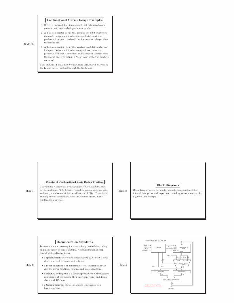
Block Diagrams
Block diagram shows the inputs , outputs, functional modules,
internal data paths, and important control signals of a system. See
Figure 6.1 for example.
Slide 4
R/W
ADDR
BYTE EN
IN
OUT
16-word x 32-bitRAMCONTROL
RESETLOAD
RUNDISPLAY
LDA LDB
4
32
32
32 32 32
A REGISTER B REGISTER
direct left right
INBUS
2
32
32 32
SEL MULTIPLEXER4 to 1
CARRY LOOKAHEAD ADDER
OUTBUS
SHIFT-AND-ADD MULTIPLIER
Copyright © 2000 by Prentice Hall, Inc. Digital Design Principles and Practices, 3/e
Slide 5
Note a bus is a collection of two or more signal lines. It represents
interconnection and data flow between two functional modules.
Slide 6
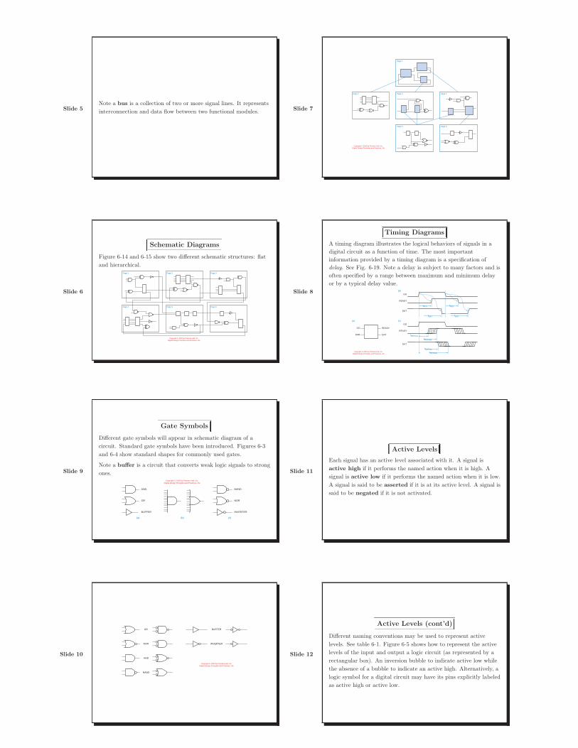
Schematic Diagrams
Figure 6-14 and 6-15 show two different schematic structures: flat
and hierarchical.Page 1
Page 4
Page 2
Page 5
Page 3
Page 6
Copyright © 2000 by Prentice Hall, Inc. Digital Design Principles and Practices, 3/e
Slide 7
Page 1
Page 3
Page 5
Page 4
Page 6
Page 2
Copyright © 2000 by Prentice Hall, Inc. Digital Design Principles and Practices, 3/e
Slide 8
Timing Diagrams
A timing diagram illustrates the logical behaviors of signals in a
digital circuit as a function of time. The most important
information provided by a timing diagram is a specification of
delay. See Fig. 6-19. Note a delay is subject to many factors and is
often specified by a range between maximum and minimum delay
or by a typical delay value.
GO
READY
DAT
(b)
GO
READY
DAT
(c)(a)
t
GO
ENB
READY
DAT
DAT
RDY
RDYmin
DATmax
DATmin
RDYmax
DAT
RDY
t
t
t
t
t t
t
Copyright © 2000 by Prentice Hall, Inc. Digital Design Principles and Practices, 3/e
Slide 9
Gate Symbols
Different gate symbols will appear in schematic diagram of a
circuit. Standard gate symbols have been introduced. Figures 6-3
and 6-4 show standard shapes for commonly used gates.
Note a buffer is a circuit that converts weak logic signals to strong
ones.
AND
OR
BUFFER
(a)
NAND
NOR
INVERTER
(c)(b)
Copyright © 2000 by Prentice Hall, Inc. Digital Design Principles and Practices, 3/e
Slide 10AND
NAND
OR
NOR INVERTER
BUFFER
Copyright © 2000 by Prentice Hall, Inc. Digital Design Principles and Practices, 3/e
Slide 11
Active Levels
Each signal has an active level associated with it. A signal is
active high if it performs the named action when it is high. A
signal is active low if it performs the named action when it is low.
A signal is said to be asserted if it is at its active level. A signal is
said to be negated if it is not activated.
Slide 12
Active Levels (cont’d)
Different naming conventions may be used to represent active
levels. See table 6-1. Figure 6-5 shows how to represent the active
levels of the input and output a logic circuit (as represented by a
rectangular box). An inversion bubble to indicate active low while
the absence of a bubble to indicate an active high. Alternatively, a
logic symbol for a digital circuit may have its pins explicitly labeled
as active high or active low.
Slide 13
Table 5 -1Each line shows a different naming convention for active levels.
Active Low Active HighREADY– READY+ERROR.L ERROR.HADDR15(L) ADDR15(H) RESET* RESET ENABLE~ ENABLE ~GO GO /RECEIVE RECEIVE
TRANSMIT_L TRANSMIT
ENABLE. . .. . .. . .
DOMY
THING. . .. . .
ENABLE. . .. . .. . .
DOMY
THING. . .. . .
(a) (b)Copyright © 2000 by Prentice Hall, Inc. Digital Design Principles and Practices, 3/e
Slide 14
(a) (b)
(c) (d)
READYGO
REQUEST
READY_LGO_L
REQUEST_LREADY_L
GOREQUEST_L
READYGO_L
REQUEST
Copyright © 2000 by Prentice Hall, Inc. Digital Design Principles and Practices, 3/e
Slide 15
Programmable Logic Arrays (PLA)
PLA is a combinational two level AND-OR device that can be
programmed to realize any sum of products expression. A PLA
often has a maximum number of inputs, outputs, and the product
terms. See figs. 6.21 and 6.22.
Slide 16
I2
I3
I1
I4
P1 P2 P3 P4 P5 P6
O3
O2
O1
Copyright © 2000 by Prentice Hall, Inc. Digital Design Principles and Practices, 3/e
The following is a programmed PLA. Give the output expressions.
Slide 17
I2
I3
I1
I4
P1 P2 P3 P4 P5 P6
O3
O2
O1
Copyright © 2000 by Prentice Hall, Inc. Digital Design Principles and Practices, 3/e
See Fig. 6-23 for programmed PLA. Note both the AND and OR
gates are programmable. Another programmable logic device is
Slide 18
Programmable Array Logic (PAL), which has fixed OR gates and
only AND gates can be programmed.
Slide 19
Decoders
A decoder is a multiple input and multiple output logic circuit that
decodes the coded input. It maps an input code into an output
code. The number of inputs is usually fewer than that of output. A
decoder usually contains a special input called enable. It must be
asserted before the decoder can perform its normal function. It is
not counted as an input. See figure 6-31.
Slide 20
Decoder
inputcode word
enableinputs
outputcode word
map
Copyright © 2000 by Prentice Hall, Inc. Digital Design Principles and Practices, 3/e
Slide 21
Binary Decoders
The most common decoder is the binary decoder where the number
of output is the power of 2 of the number of input. For example, we
have n to 2n binary decoder, where n is the number of input and
2n is the number of output. A binary decoder is used when you
need to activate exactly one of 2n outputs based on n inputs. Note
the “don’t care” notation in the truth table.
Slide 22
Binary Decoders (cont’d)
Table 6-4 gives the truth table of a 2-to-4 binary decoder. The
logic symbol and the logic diagram of a 2-to-4 binary decoder are
shown in Figure 6-32.
2-to-4decoder
I0I1
EN
Y0Y1Y2Y3
(a) (b)
I0′ I0 I1′ I1 EN
I0
I1
EN
Y0
Y1
Y2
Y3
Slide 23
Table 5 -4Truth table for a 2-to-4 binary decoder.
Inputs Outputs
EN I1 I0 Y3 Y2 Y1 Y0
0 x x 0 0 0 0 1 0 0 0 0 0 1 1 0 1 0 0 1 0 1 1 0 0 1 0 0 1 1 1 1 0 0 0
Note the truth table will be different if the active levels for
input/ouput are changed. What are the truth table if the outputs
are all active low ?
The input and output codes are not limited to consecutive decimal
numbers but may represent any consecutive physical entities. For
example, see table 6-5.
Slide 24
Disk Position I2 I1 I0 Binary Decoder Output Table 5-5Position encoding for a 3-bit mechanical encoding disk.
0° 0 0 0 Y045° 0 0 1 Y190° 0 1 1 Y3
135° 0 1 0 Y2180° 1 1 0 Y6225° 1 1 1 Y7270° 1 0 1 Y5315° 1 0 0 Y4
Slide 25
DEG225DEG180
DEG90
3-to-8decoder
I0I1I2EN
Y0Y1Y2Y3Y4Y5Y6Y7
SHAFTI0SHAFTI1SHAFTI2ENABLE
DEG0DEG45DEG135
DEG270DEG315
Copyright © 2000 by Prentice Hall, Inc. Digital Design Principles and Practices, 3/e
Also not all outputs of a decoder may be used, e.g., for BCD
Slide 26 decoder, it only produces 10 outputs.
Slide 27
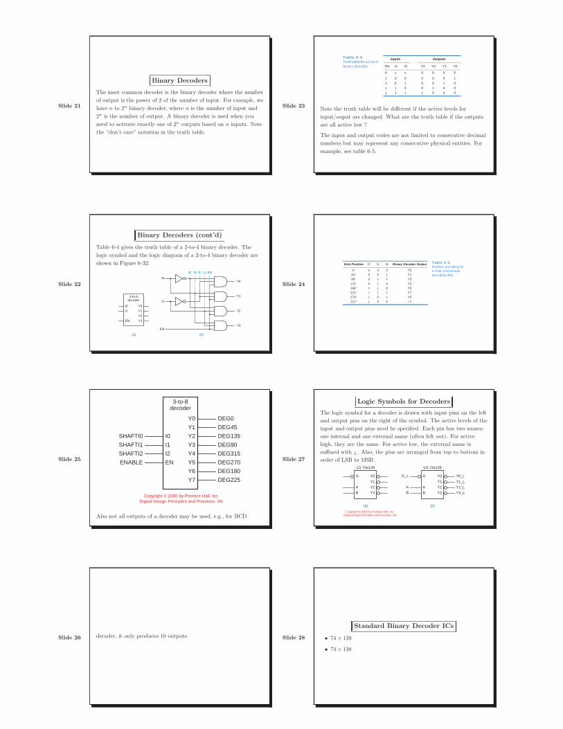
Logic Symbols for Decoders
The logic symbol for a decoder is drawn with input pins on the left
and output pins on the right of the symbol. The active levels of the
input and output pins need be specified. Each pin has two names:
one internal and one external name (often left out). For active
high, they are the same. For active low, the external name is
suffixed with L. Also, the pins are arranged from top to bottom in
order of LSB to MSB.
1/2 74x139
A
G
B
Y0Y1Y2Y3
(a)
1/2 74x139
A
G
B
Y0Y1Y2Y3
(b)
Y0_LY1_LY2_LY3_L
G_L
AB
Copyright © 2000 by Prentice Hall, Inc. Digital Design Principles and Practices, 3/e
Slide 28
Standard Binary Decoder ICs
• 74× 139
• 74× 138

Slide 29
74× 139 Dual 2-to-4 Decoder
The 74× 139 dual 2-to-4 decoder consists of two independent but
identical 2-to-4 decoders, contained in a single MSI (middle size
integration) chip. It is designed with active-low at outputs. The
figure below gives the logic diagram and logic symbol for the
decoder. The truth table for half of the 74× 139 dual 2-to-4
decoder is shown in table below. Note for both input and output
the top input and the top output bit represent the LSB while the
bottom input bit and the bottom output bit represent the MSB.
Slide 30
74x139
1A
1G
1B
1Y01Y11Y21Y3
(b)
1G_L
1A
1B
(1)
(4)
1 4
5
6
7
2
3
2A
2G
2B
2Y02Y12Y22Y3
15 12
11
10
9
14
13
1/2 74x139
A
G
B
Y0Y1Y2Y3
(c)
(5)
(6)
(7)
(2)
(3)
1Y0_L
1Y1_L
1Y2_L
1Y3_L
2G_L
2A
2B
(15)
(12)
(11)
(10)
(9)
(14)
(13)
2Y0_L
2Y1_L
2Y2_L
2Y3_L
(a)
Copyright © 2000 by Prentice Hall, Inc. Digital Design Principles and Practices, 3/e
Slide 31
Table 5-6Truth table for one-half of a 74x139 dual 2-to-4 decoder.
Inputs Outputs
G_L B A Y3_L Y2_L Y1_L Y0_L
1 x x 1 1 1 10 0 0 1 1 1 00 0 1 1 1 0 10 1 0 1 0 1 1 0 1 1 0 1 1 1
Slide 32
74× 138 MSI 3-to-8 Decoder
It has three enable inputs and its outputs are active low. All the
three enable inputs must be asserted before the decoder can
perform its function. Its logic diagram and logic symbol are shown
in Figure 6-35.
74x138
G2AG1
G2B
Y0Y1Y2Y3
(b)(15)
615
14
13
7
4
5
BA
C
Y4Y5Y6Y7
1
12
11
10
92
3
(14)
(13)
(12)
Y0_L
Y1_L
Y2_L
Y3_L
C
(11)
(10)
(9)
(7)(3)
B(2)
Y4_L
Y5_L
Y6_L
Y7_L
A(1)
G2B_L(5)
G2A_L(4)
G1(6)
(a)
Copyright © 2000 by Prentice Hall, Inc. Digital Design Principles and Practices, 3/e
Slide 33
Truth table is shown in Table 6-6. An output is asserted if only the
decoder is enabled and the output is selected (e.g., Y 5L).
Table 5-7 Truth table for a 74x138 3-to-8 decoder.
Inputs Outputs
G1 G2A_L G2B_L C B A Y7_L Y6_L Y5_L Y4_L Y3_L Y2_L Y1_L Y0_L
0 x x x x x 1 1 1 1 1 1 1 1x 1 x x x x 1 1 1 1 1 1 1 1x x 1 x x x 1 1 1 1 1 1 1 1 1 0 0 0 0 0 1 1 1 1 1 1 1 01 0 0 0 0 1 1 1 1 1 1 1 0 11 0 0 0 1 0 1 1 1 1 1 0 1 1 1 0 0 0 1 1 1 1 1 1 0 1 1 11 0 0 1 0 0 1 1 1 0 1 1 1 11 0 0 1 0 1 1 1 0 1 1 1 1 1 1 0 0 1 1 0 1 0 1 1 1 1 1 11 0 0 1 1 1 0 1 1 1 1 1 1 1
Slide 34
Cascading Binary Decoders
Multiple binary decoders can be combined in cascade to decode
larger code words. The figure below shows how to combine two 3-8
decoders into a 4-to-16 decoder. Figure 6-37 shows a 5-to-32
decoder constructed from 5 3-8 decoders.
Slide 35
74x138
G2AG1
G2B
Y0Y1Y2Y3
615
14
13
7
4
5
BA
C
Y4Y5Y6Y7
1
12
11
10
92
3
74x138
G2AG1
G2B
Y0Y1Y2Y3
615
14
13
7
4
5
BA
C
Y4Y5Y6Y7
1
12
11
10
92
3
DEC0_LDEC1_LDEC2_LDEC3_LDEC4_LDEC5_L
DEC10_LDEC11_LDEC12_LDEC13_LDEC14_LDEC15_L
DEC6_LDEC7_L
DEC8_LDEC9_L
N0N1N2N3
EN_L
+5V
U1
U2
R
Copyright © 2000 by Prentice Hall, Inc. Digital Design Principles and Practices, 3/e
Slide 36
Logic Expression from Decoders
How to build F =∑
XY Z(2, 4, 7) using a 74x138 decoder ?
Slide 37
Multiplexers
A multiplexer is a digital switch that determines which of its n
input data should be routed to output. It is a useful device in any
application where data must be switched from multiple sources to a
destination source. For example , the multiplexer between the
processor’s registers and its arithmetic logic unit (ALU). The data
from one of the registers must be routed to ALU for execution.
Slide 38
multiplexer
EN
SELs
enable
select
D0b
bD1b
Dn−1b
n datasources
(a)
(b)
dataoutputY
1D01D1
1Dn−1
2D02D1
2Dn−1
bD0bD1
bDn−1
1Y
2Y
bY
SEL EN
Slide 39
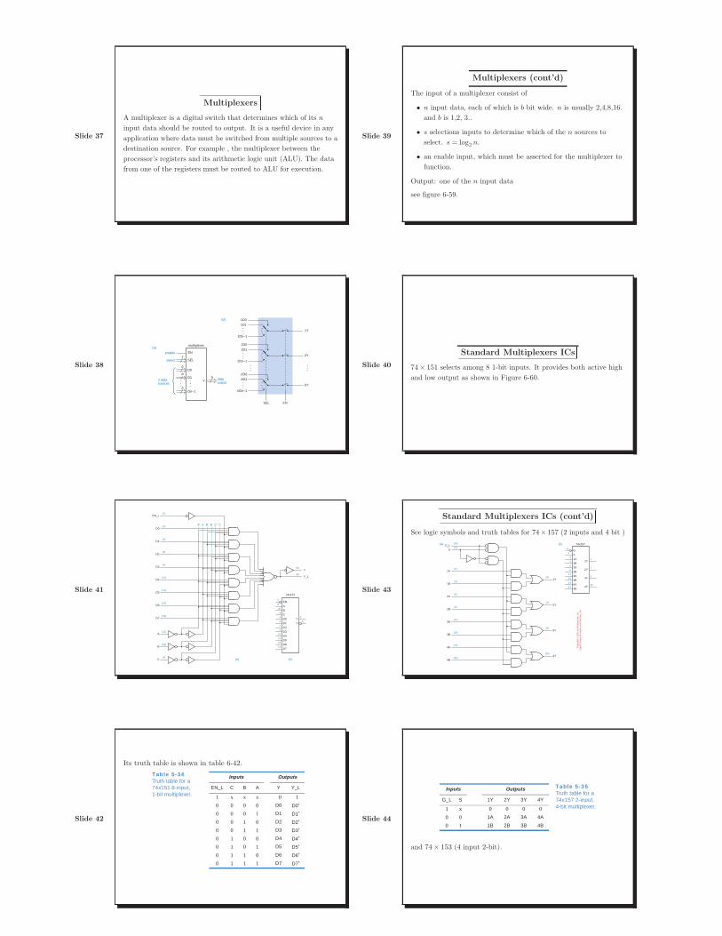
Multiplexers (cont’d)
The input of a multiplexer consist of
• n input data, each of which is b bit wide. n is usually 2,4,8,16.
and b is 1,2, 3..
• s selections inputs to determine which of the n sources to
select. s = log2n.
• an enable input, which must be asserted for the multiplexer to
function.
Output: one of the n input data
see figure 6-59.
Slide 40
Standard Multiplexers ICs
74× 151 selects among 8 1-bit inputs. It provides both active high
and low output as shown in Figure 6-60.
Slide 41
(4)
(3)
(2)
(5)
(6)
(1)
(15)
(14)
(13)
(12)
(11)
(10)
(9)
(7)
(a) (b)
A′ A B′ B C′ CD0
D1
D2
D3
D4
D5
D6
D7
A
B
C
EN_L
Y
Y_L
74x151
D0D1D2D3D4D5D6D7
EN
4
6
5YY
3
2
1
15
14
13
12
ABC
11
10
9
7
Slide 42
Its truth table is shown in table 6-42.
Table 5-34Truth table for a 74x151 8-input, 1-bit multiplexer.
Inputs Outputs
EN_L C B A Y Y_L
1 x x x 0 10 0 0 0 D0 D0′0 0 0 1 D1 D1′0 0 1 0 D2 D2′0 0 1 1 D3 D3′0 1 0 0 D4 D4′0 1 0 1 D5 D5′0 1 1 0 D6 D6′0 1 1 1 D7 D7′
Slide 43
Standard Multiplexers ICs (cont’d)
See logic symbols and truth tables for 74× 157 (2 inputs and 4 bit )
(2)
(3)
(5)
(6)
(11)
(10)
(14)
(13)
(1)
(15)(a) (b)
1A
1B
2A
2B
3A
3B
4A
4B
SG_L 74x157
1A1B2A2B3A3B4A4B
G
24
1Y
72Y
93Y
124Y
3
5
6
11
10
14
13
S1
15
(4)
(7)
(9)
(12)
1Y
2Y
3Y
4Y
Cop
yrig
ht ©
200
0 by
Pre
ntic
e H
all,
Inc.
D
igita
l Des
ign
Prin
cipl
es a
nd P
ract
ices
, 3/e
Slide 44
Inputs Outputs Table 5-35Truth table for a 74x157 2-input, 4-bit multiplexer.
G_L S 1Y 2Y 3Y 4Y
1 x 0 0 0 00 0 1A 2A 3A 4A
0 1 1B 2B 3B 4B
and 74× 153 (4 input 2-bit).
Slide 45
(6)
(5)
(4)
(3)
(14)(a)
(b)
1C0
1C1
1C2
(15)
(1)
2G_L
1C3
A
(2)B
74x153
1G1C01C11C21C3
2C02C12C22C3
A
1
71Y
92Y
6
5
4
3
15
10
11
12
13
B2
14
2G
(7)1Y
(10)
(11)
(12)
(13)
2C0
1G_L
2C1
2C2
2C3
(9)2Y
Copyright © 2000 by Prentice Hall, Inc. Digital Design Principles and Practices, 3/e
Slide 46
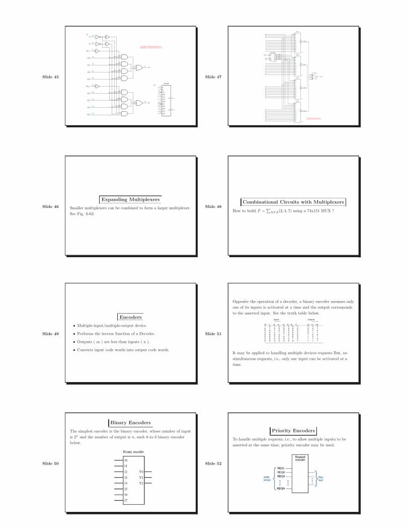
Expanding Multiplexers
Smaller multiplexers can be combined to form a larger multiplexer.
See Fig. 6-62.
Slide 47
74x151
D0D1D2D3D4D5D6D7
EN
4
6YY
3
2
1
15
14
13
12
ABC
11
7
10
9
1/2 74x139
1A
1G
1B
1Y01Y11Y21Y3
1 4
5
6
7
2
3
XEN_L
XA3XA4
XA0
XA2XA1
X0
X2X1
X3X4X5
X7X6
EN3_LEN2_LEN1_LEN0_L 74x151
D0D1D2D3D4D5D6D7
EN
4
6YY
3
2
1
15
14
13
12
ABC
11
7
10
9
X10
X12X11
X13X14X15
X9X8
74x151
D0D1D2D3D4D5D6D7
EN
4
6YY
3
2
1
15
14
13
12
ABC
11
7
10
9
74x151
D0D1D2D3D4D5D6D7
EN
4
6YY
3
2
1
15
14
13
12
ABC
11
7
10
9
X16
X18X17
X19X20X21
X23X22
X24
X26X25
X27X28X29
X31X30
1/2 74x201
2
46
5
XOUT
XO0_L
XO1_L
XO2_L
XO3_L
U1
U5
U4
U3
U2
5
5
5
5
U6
Copyright © 2000 by Prentice Hall, Inc. Digital Design Principles and Practices, 3/e
Slide 48
Combinational Circuits with Multiplexers
How to build F =∑
XY Z(2, 4, 7) using a 74x151 MUX ?
Slide 49
Encoders
• Multiple-input/multiple-output device.
• Performs the inverse function of a Decoder.
• Outputs ( m ) are less than inputs ( n ).
• Converts input code words into output code words.
Slide 50
Binary Encoders
The simplest encoder is the binary encoder, whose number of input
is 2n and the number of output is n, such 8-to-3 binary encoder
below.
Slide 51
Opposite the operation of a decoder, a binary encoder assumes only
one of its inputs is activated at a time and the output corresponds
to the asserted input. See the truth table below.
It may be applied to handling multiple devices requests But, no
simultaneous requests, i.e., only one input can be activated at a
time.
Slide 52
Priority Encoders
To handle multiple requests, i.e., to allow multiple inputs to be
asserted at the same time, priority encoder may be used.

Slide 53
Priority Encoder (cont’d)
• Assign priorities to the inputs
• When more than one input are asserted, the output generates
the code for the input with the highest priority
Slide 54
74x148 8-input priority encoder
Slide 55
74x148 8-input priority encoder (cont’d)
It is clear that the output only corresponds to the input with the
highest priority. The low priority inputs are ignored, independent
of their states (don’t care). Output enable is asserted only when all
inputs are not activated. The GS output is asserted if any of of the
Slide 56 input is asserted.
Slide 57
Three State Buffers
A three state buffer contains two inputs and one output. One of
the inputs is enable input. It must be asserted before the buffer can
function. The three state buffer can be inverting or non-inverting
with either active high or low enable input. See figure 6-51 for
example.
Slide 58
Standard 3 State Buffers ICs
Several independent three state buffers may be packaged in a single
SSI IC or MSI IC. 74× 125 and 74× 126 each contains 4 three
state buffers. 74× 541 contains 8 three state buffers.
(3)(2)
(1)
(6)(5)
(4)
(11)(12)
(13)
(8)(9)
(10)
(3)(2)
(1)
(6)(5)
(4)
(11)(12)
(13)
(8)(9)
(10)74x12674x125
Cop
yrig
ht ©
200
0 by
Pre
ntic
e H
all,
Inc.
D
igita
l Des
ign
Prin
cipl
es a
nd P
ract
ices
, 3/e
Slide 59
Use of 3 State Buffers
Three state buffer may be used to allow multiple sources to share a
single line, as long as only one can be active at a time. See Fig
6-52, which shows the use of three state buffers allow to 8 sources
of data to drive a single line at a time.
Slide 60
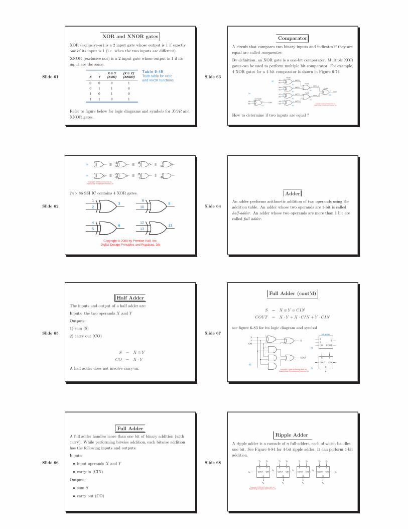
Slide 61
XOR and XNOR gates
XOR (exclusive-or) is a 2 input gate whose output is 1 if exactly
one of its input is 1 (i.e. when the two inputs are different).
XNOR (exclusive-nor) is a 2 input gate whose output is 1 if its
input are the same.
X YX ⊕ Y(XOR)
(X ⊕ Y)′(XNOR)
Table 5-45Truth table for XORand XNOR functions.
0 0 0 10 1 1 01 0 1 01 1 0 1
Refer to figure below for logic diagrams and symbols for XOR and
XNOR gates.
Slide 62
(a)
(b)
Copyright © 2000 by Prentice Hall, Inc. Digital Design Principles and Practices, 3/e
74× 86 SSI IC contains 4 XOR gates.
12
1311
9
108
4
56
1
23
Copyright © 2000 by Prentice Hall, Inc. Digital Design Principles and Practices, 3/e
Slide 63
Comparator
A circuit that compares two binary inputs and indicates if they are
equal are called comparator.
By definition, an XOR gate is a one-bit comparator. Multiple XOR
gates can be used to perform multiple bit comparator. For example,
4 XOR gates for a 4-bit comparator is shown in Figure 6-74.
1/4 74x86A0B0
74x86
74x02
74x02
74x00
A0B0
A1B1
A2B2
A3B3
DIFF
DIFF(a)
(b)
1
2
12
1311
9
108
4
56
1
23
3
1
23
2
31
5
64
U1 U1
U1
U1
U1
U2
U3
U2
DIFF0
DIFF1
DIFF2
DIFF3
DF01_L
DF23_L
Copyright © 2000 by Prentice Hall, Inc. Digital Design Principles and Practices, 3/e
How to determine if two inputs are equal ?
Slide 64
Adder
An adder performs arithmetic addition of two operands using the
addition table. An adder whose two operands are 1-bit is called
half-adder. An adder whose two operands are more than 1 bit are
called full adder.
Slide 65
Half Adder
The inputs and output of a half adder are:
Inputs: the two operands X and Y
Outputs:
1) sum (S)
2) carry out (CO)
S = X ⊕ Y
CO = X · Y
A half adder does not involve carry-in.
Slide 66
Full Adder
A full adder handles more than one bit of binary addition (with
carry). While performing bitwise addition, each bitwise addition
has the following inputs and outputs:
Inputs:
• input operands X and Y
• carry in (CIN)
Outputs:
• sum S
• carry out (CO)
Slide 67
Full Adder (cont’d)
S = X ⊕ Y ⊕ CIN
COUT = X · Y +X · CIN + Y · CIN
see figure 6-83 for its logic diagram and symbol
(a)
(b)
XY
CINS
COUT
XYCIN
S
COUT
full adder
(c)
COUT CIN
X
S
Y
Copyright © 2000 by Prentice Hall, Inc. Digital Design Principles and Practices, 3/e
Slide 68
Ripple Adder
A ripple adder is a cascade of n full-adders, each of which handles
one bit. See Figure 6-84 for 4-bit ripple adder. It can perform 4-bit
addition.
SSS
COUT CIN
X
S
Y
COUT CIN
X Y
COUT CIN
X Y
COUT CIN
X Y
x2 y2 x1 y1 x0 y0
c3c4
c2 c1
x3 y3
c0
s2 s1 s0s3
Copyright © 2000 by Prentice Hall, Inc. Digital Design Principles and Practices, 3/e
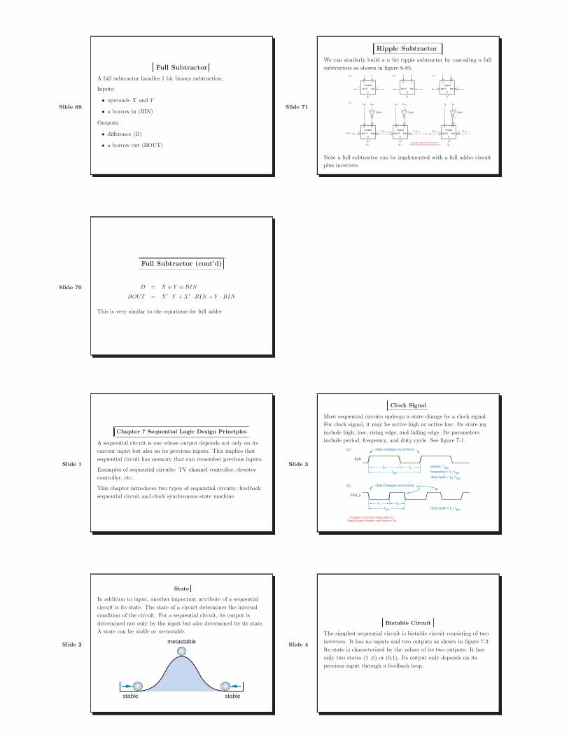
Slide 69
Full Subtractor
A full subtractor handles 1 bit binary subtraction.
Inputs:
• operands X and Y
• a borrow in (BIN)
Outputs:
• difference (D)
• a borrow out (BOUT)
Slide 70
Full Subtractor (cont’d)
D = X ⊕ Y ⊕BIN
BOUT = X′
· Y +X′
· BIN + Y · BIN
This is very similar to the equations for full adder
Slide 71
Ripple Subtractor
We can similarly build a n bit ripple subtractor by cascading n full
subtractors as shown in figure 6-85.
b_Ln–1
COUT CIN
X
S
Y74x999
BOUT BIN
X
D
Y
BOUT BIN
X
D
Y74x999
BOUT BIN
X
D
Y74x999
74x04 74x04 74x04
xn–1 yn–1
dn–1
b_Ln BOUT BIN
X
D
Y74x999
xn–2 yn–2
dn–2
BOUT BIN
X
D
Y74x999
x0 y0
d0
b_Ln–2 b_L1 b_L01
53
(a)1 2
5 3
4
(b) (c)1 2
5 3
4
1 2
2
1
5 3
4
1 2
4
3
4
1 2
12
13
5 3
4
(d)
Copyright © 2000 by Prentice Hall, Inc. Digital Design Principles and Practices, 3/e
Note a full subtractor can be implemented with a full adder circuit
plus inverters.
Slide 1
Chapter 7 Sequential Logic Design Principles
A sequential circuit is one whose output depends not only on its
current input but also on its previous inputs. This implies that
sequential circuit has memory that can remember previous inputs.
Examples of sequential circuits: TV channel controller, elevator
controller, etc..
This chapter introduces two types of sequential circuits: feedback
sequential circuit and clock synchronous state machine.
Slide 2
State
In addition to input, another important attribute of a sequential
circuit is its state. The state of a circuit determines the internal
condition of the circuit. For a sequential circuit, its output is
determined not only by the input but also determined by its state.
A state can be stable or metastable.
stable stable
metastable
Slide 3
Clock Signal
Most sequential circuits undergo a state change by a clock signal.
For clock signal, it may be active high or active low. Its state my
include high, low, rising edge, and falling edge. Its parameters
include period, frequency, and duty cycle. See figure 7-1.
CLK
tper
tHtL
tLtHtper
state changes occur here(a)
state changes occur here
CLK_L
(b)
duty cycle = tH / tper
frequency = 1 / tper
period = tper
duty cycle = tL / tper
Copyright © 2000 by Prentice Hall, Inc. Digital Design Principles and Practices, 3/e
Slide 4
Bistable Circuit
The simplest sequential circuit is bistable circuit consisting of two
inverters. It has no inputs and two outputs as shown in figure 7-2.
Its state is characterized by the values of its two outputs. It has
only two states (1 ,0) or (0,1). Its output only depends on its
previous input through a feedback loop.
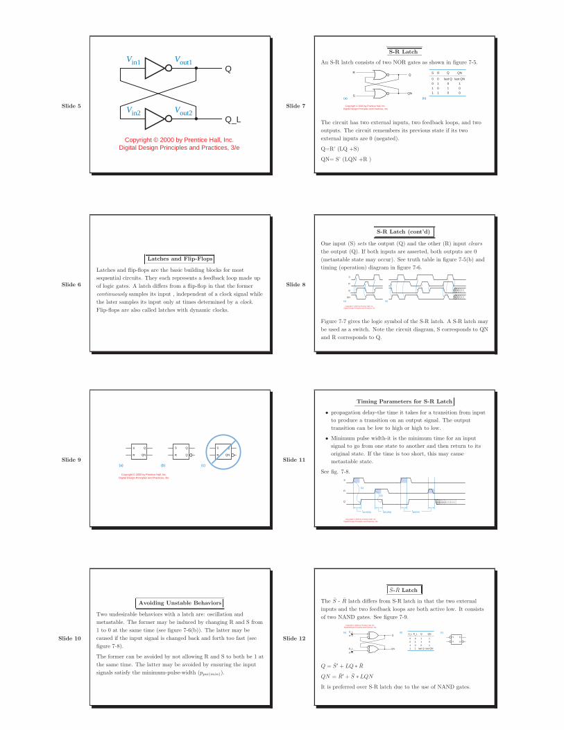
Slide 5
Vin1 Vout1
Vout2Vin2
Q
Q_L
Copyright © 2000 by Prentice Hall, Inc. Digital Design Principles and Practices, 3/e
Slide 6
Latches and Flip-Flops
Latches and flip-flops are the basic building blocks for most
sequential circuits. They each represents a feedback loop made up
of logic gates. A latch differs from a flip-flop in that the former
continuously samples its input , independent of a clock signal while
the later samples its input only at times determined by a clock.
Flip-flops are also called latches with dynamic clocks.
Slide 7
S-R Latch
An S-R latch consists of two NOR gates as shown in figure 7-5.
R
S
Q0 00 11 01 1
S R
0
01
last Q
Q
100
(a) (b)
QN
last QN
QN
Copyright © 2000 by Prentice Hall, Inc. Digital Design Principles and Practices, 3/e
The circuit has two external inputs, two feedback loops, and two
outputs. The circuit remembers its previous state if its two
external inputs are 0 (negated).
Q=R’ (LQ +S)
QN= S’ (LQN +R )
Slide 8
S-R Latch (cont’d)
One input (S) sets the output (Q) and the other (R) input clears
the output (Q). If both inputs are asserted, both outputs are 0
(metastable state may occur). See truth table in figure 7-5(b) and
timing (operation) diagram in figure 7-6.
S
R
Q
(a) (b)
QN
Copyright © 2000 by Prentice Hall, Inc. Digital Design Principles and Practices, 3/e
Figure 7-7 gives the logic symbol of the S-R latch. A S-R latch may
be used as a switch. Note the circuit diagram, S corresponds to QN
and R corresponds to Q.
Slide 9
Q
QNR
(b) (c)(a)
S Q
QNR
S SQ
QR
Copyright © 2000 by Prentice Hall, Inc. Digital Design Principles and Practices, 3/e
Slide 10
Avoiding Unstable Behaviors
Two undesirable behaviors with a latch are: oscillation and
metastable. The former may be induced by changing R and S from
1 to 0 at the same time (see figure 7-6(b)). The latter may be
caused if the input signal is changed back and forth too fast (see
figure 7-8).
The former can be avoided by not allowing R and S to both be 1 at
the same time. The latter may be avoided by ensuring the input
signals satisfy the minimum-pulse-width (ppw(min)).
Slide 11
Timing Parameters for S-R Latch
• propagation delay-the time it takes for a transition from input
to produce a transition on an output signal. The output
transition can be low to high or high to low.
• Minimum pulse width-it is the minimum time for an input
signal to go from one state to another and then return to its
original state. If the time is too short, this may cause
metastable state.
See fig. 7-8.
S
R
Q
tpHL(RQ)tpLH(SQ)
(2)
(1)
tpw(min)
Copyright © 2000 by Prentice Hall, Inc. Digital Design Principles and Practices, 3/e
Slide 12
S̄-R̄ Latch
The S̄ - R̄ latch differs from S-R latch in that the two external
inputs and the two feedback loops are both active low. It consists
of two NAND gates. See figure 7-9.
S_L
R_L
Q0 00 11 01 1 last Q
10
1
Q
01
1
(a) (b) (c)
S Q
QR
last QN
QNor S
or RQN
S_L R_L
Copyright © 2000 by Prentice Hall, Inc. Digital Design Principles and Practices, 3/e
Q = S̄′ + LQ ∗ R̄
QN = R̄′ + S̄ ∗ LQN
It is preferred over S-R latch due to the use of NAND gates.
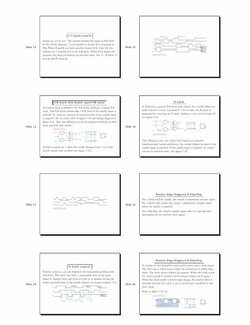
Slide 13
S̄-R̄ Latch (cont’d)
Inputs are active low. The output remains the same as S-R latch.
In the circuit diagram, S̄ corresponds to Q and R̄ corresponds to
NQ. When S and R are both asserted (equal to 0), then the two
outputs are 1 instead of 0 as for S-R latch. When both inputs are
negated, the latch remembers its previous state. For S̄ - R̄ latch, S̄
sets Q and R̄ clears Q.
Slide 14
S-R Latch with Enable (gated SR latch)
An enable input is added to the S-R latch, yielding a 3-input S-R
latch. The S-R latch behaves like a S-R latch if the enable input is
asserted. It, however, assumes its previous state if the enable input
is negated. See its truth table in figure 7-10 and timing diagram in
figure 7-11. Note the difference in circuit diagrams between an S-R
latch and S-R with enable.
1 1
0 11 0
S
1
11
CR
011
Q
0 0 1 last Q
xx 0 last Q
101
(b) (c)(a)
QS
C
R
S Q
QR
C
QN
last QN
last QNQN
Copyright © 2000 by Prentice Hall, Inc. Digital Design Principles and Practices, 3/e
If both S and R are 1 when the enable changes from 1 to 0, this
circuit output may oscillate (see figure 7-11).
Slide 15
S
R
C
Q
Ignored since C is 0. Ignored until C is 1.
QN
Copyright © 2000 by Prentice Hall, Inc. Digital Design Principles and Practices, 3/e
Slide 16
D Latch
A D-latch is a special S-R latch with enable. It is useful when you
need a device to store (remember) a bit of data. Its R input is
generated by inverting its S input, leading to one external input D.
see figure 7-12.
(b) (c)(a)
Q
D
C 01
D
11
C
01
Q
x0 last Q
10
D Q
QC
QN
QN
last QN
Copyright © 2000 by Prentice Hall, Inc. Digital Design Principles and Practices, 3/e
This eliminates the case where both inputs are asserted
simultaneously (avoid oscillation). Its output follows its input if the
enable input is asserted. If the enable input is negated, its output
retains its previous state. See figure 7-13.
Slide 17
D
C
Q
Copyright © 2000 by Prentice Hall, Inc. Digital Design Principles and Practices, 3/e
Slide 18
D Latch (cont’d)
D-latch, however, can not eliminate the metastable problem with
S-R latch. The latch may enter a metastable state if the input
signal D changes back and forth too fast or it changes during the
setup- and hold-time of the enable signal C as shown in figure 7-14.
D
C
Q
tholdtsetuptpLH(DQ)tpLH(DQ)
tpHL(DQ)tpLH(CQ)
tpHL(CQ)
(1) (2) (3) (5)(4)
Slide 19
Positive Edge-Triggered D Flip-Flop
For a latch without enable, the output continuously samples input.
For a latch with enable, the output continuously samples input
when the enable is asserted.
For a flip-flop, the output samples input only at a specific time
determined by an external clock signal.
Slide 20
Positive Edge-Triggered D Flip-Flop
It consists of two D-latches connected in series and a clock signal.
The first one is called master while the second one is called slave
latch. The salve always follows the master. While the clock is low,
the master latch is enabled and its output follows its D input.
When the clock makes a low-to-high change, the master latch is
disabled and the last value it saw is stored and transfered to the
slave latch.
Refer to figure 7-15 (a).
(b) (c)(a)
QD
CLK
CLK
0
1
D
0
1
Q
0x last Q
1
0
1x last Q
D Q
C
D Q
QCD Q
QCLK
QM
QN
QN
last QN
last QN
Copyright © 2000 by Prentice Hall, Inc. Digital Design Principles and Practices, 3/e

Slide 21
Positive Edge-Triggered D Flip-Flop(cont’d)
The slave is enabled while the clock is high, its output follows its
input. However, its output only changes at the time the clock goes
high since it’s input is connected to the master and the master can
not change when the clock is high. This produces the
edge-triggered effect. The output follows input only when the clock
is at its rising edge. See figure 7-16 and Fig. 7-15 (b).
D
CLK
QM
Q
QN
Copyright © 2000 by Prentice Hall, Inc. Digital Design Principles and Practices, 3/e
See Fig. 7-15(c) for the logic symbol of D-FF. Note the difference
from the that of D latch. Metastable state still occurs if the input
Slide 22
signal changes during the setup and hold time of the clock signal.
See Fig. 7-17.
D
CLK
Q
tholdtsetuptpHL(CQ)tpLH(CQ)
In summary, the positive edge-triggered D flip-flop samples its input
only when the clock signal at its rising edge. Its output follows its
input only when the clock signal is at its rising edge. Its output
assumes its previous state if the clock input is asserted or negated.
Slide 23
Edge-Triggered D Flip-Flop with Enable
An enable input is added to the edge-triggered D flip-flop to allow
it to assume its previous value even at the rising edge of the clock
signal. The enable signal does not matter if the clock signal is not
at its rising edge. see figure 7-21.
(b) (c)(a)
Q
D
CLK
CLK
0
1
D
0
1
Q
0x last Q
1
0
1x last Q
D Q
Q
D Q
QCLKQN
QN
last QN
last QN
EN 1
1
EN
x
x
x 0 last Q last QN
EN
CLK
Slide 24
Edge-triggered J-K Flip-Flop
It contains an edge-triggered D flip-flop. Here the J-K flip-flop is
triggered by the rising edge of the control signal. The flip flop
assumes its previous state if the control signal is asserted or
negated. At the rising edge of the clock (control) signal, the Q
output follows J input while the QN outputs follows K input.
While both J and K are asserted at the same time and the clock is
at its rising edge, Q assumes previous QN and QN assumes
previous Q. See figures 7-28 and 7-29
(b)(a) (c)CLK
0
K Q
last Q last QN
QN
0
J
x 1 last Q last QNx
x 0 last Q last QNx
1 0 10
0 1 01
1 last QN last Q1
Q
QN
J
CLK
KD Q
QCLK
J Q
QK
CLK
Copyright © 2000 by Prentice Hall, Inc. Digital Design Principles and Practices, 3/e
Slide 25
K
J
CLK
Q
Copyright © 2000 by Prentice Hall, Inc. Digital Design Principles and Practices, 3/e
Slide 26
Positive Edge Triggered T Flip-Flop
A T (toggle) flip-flop changes state on every tick of the clock. It
can be constructed from a D flip-flop or from a J-K flip-flop as
shown in Figure 7-31 and F-32.
Q
Q QN
QT
J
K
CLKQN
Q
(a)
D Q
QCLKT
(b)
1
Copyright © 2000 by Prentice Hall, Inc. Digital Design Principles and Practices, 3/e
Its output follows the clock signal at half the frequency of the input.
Q
QT
(a) (b)
T
Q
Copyright © 2000 by Prentice Hall, Inc. Digital Design Principles and Practices, 3/e
Figure 7-33 shows a T FF with enable.
Slide 27
Q
Q QN
QT
J
K
CLKQN
Q
(a)
D Q
QCLKT
EN
(b)
EN
Copyright © 2000 by Prentice Hall, Inc. Digital Design Principles and Practices, 3/e
Q
QT
EN
(a) (b)
T
EN
Q
Copyright © 2000 by Prentice Hall, Inc. Digital Design Principles and Practices, 3/e
Slide 28
Clocked Synchronous State Machine Analysis
State machine is a generic name given to a sequential circuit.
clocked refers to the flip-flops of the sequential circuit are
controlled by a clock signal. Synchronous all flip-flops use the
same clock signal,which causes the flop-flips to change states at
each tick (rising/falling edge) of the clock.

Slide 29
State Machine Structure
A state machine consists of three components: state memory,
next-state logic, and output logic as shown in figure 7-35.
StateMemory
clock input
Next-stateLogic
F
OutputLogic
G
excitation current stateinputs
clocksignal
outputs
Copyright © 2000 by Prentice Hall, Inc. Digital Design Principles and Practices, 3/e
state memory is a set of flip-flops that store current state. Given n
flip-flops, it can store 2n states. Its inputs include an excitation
signal and a clock signal (which connects to all flip-flops). Its
output is current state.
Slide 30
State Machine Structure (cont’d)
The next-state logic determines the next state of the state machine.
It is a function of input and current state. The output logic
determines the output of the state machine. It is a function of
input and current state. Both the next-state logic and output logic
are combinational circuits.
Sequential circuit whose output depends on both its input and
current state is called Mealy machine. Sequential circuit whose
output depends only on current state is called Moore machine (see
figure 7-36).
Slide 31
StateMemory
clock input
Next-stateLogic
F
OutputLogic
G
excitation current stateinputs
clocksignal
outputs
Copyright © 2000 by Prentice Hall, Inc. Digital Design Principles and Practices, 3/e
Slide 32
An Example of a State Machine
EN
CLK
D0 Q0
D1 Q1
MAX
D Q
QCLK
D Q
QCLK
current state
excitation
output
input
clock signal
Next-state Logic F State Memory Output Logic G
EN′
EN
Q0′
Q0
Q1′
Q1
Copyright © 2000 by Prentice Hall, Inc. Digital Design Principles and Practices, 3/e
Slide 33
Characteristic Equations
The characteristic equation of a latch or flip-flop specifies the
flip-flop’s next state as a function of its current state and inputs
when the the enable is asserted (for latch) or when the clock is at
its rising edge (for FFs). See table 7-1.
Device TypeCharacteristic
EquationTable 7-1Latch and flip-flop characteristic equations.S-R latch Q∗ = S + R′ ⋅ Q
D latch Q∗ = D
Edge-triggered D flip-flop Q∗ = D
D flip-flop with enable Q∗ = EN ⋅ D + EN′ ⋅ Q
Master/slave S-R flip-flop Q∗ = S + R′ ⋅ QMaster/slave J-K flip-flop Q∗ = J ⋅ Q′ + K′ ⋅ Q
Edge-triggered J-K flip-flop Q∗ = J ⋅ Q′ + K′ ⋅ Q
T flip-flop Q∗ = Q′T flip-flop with enable Q∗ = EN ⋅ Q′ + EN′ ⋅ Q
Note characteristic equation only describes functional response to
Slide 34
the control inputs when output samples input, e.g., during a clock
tick for FF and when the enable is asserted for latch.
Slide 35
Analysis of State Machine
The goal of analysis of state machine is to characterize the behavior
of sequential circuit in terms of relationship between its input,
current state, next state, and output (note how this differs from
combinational circuit analysis).
Slide 36
Analysis of State Machine
Three steps in state machine analysis:
1. Determine the next state function F and output function G
2. Use F and G to construct state/output table that completely
specifies the next state and the output of the circuit for every
possible combination of current state and input.
3. Draw a state diagram
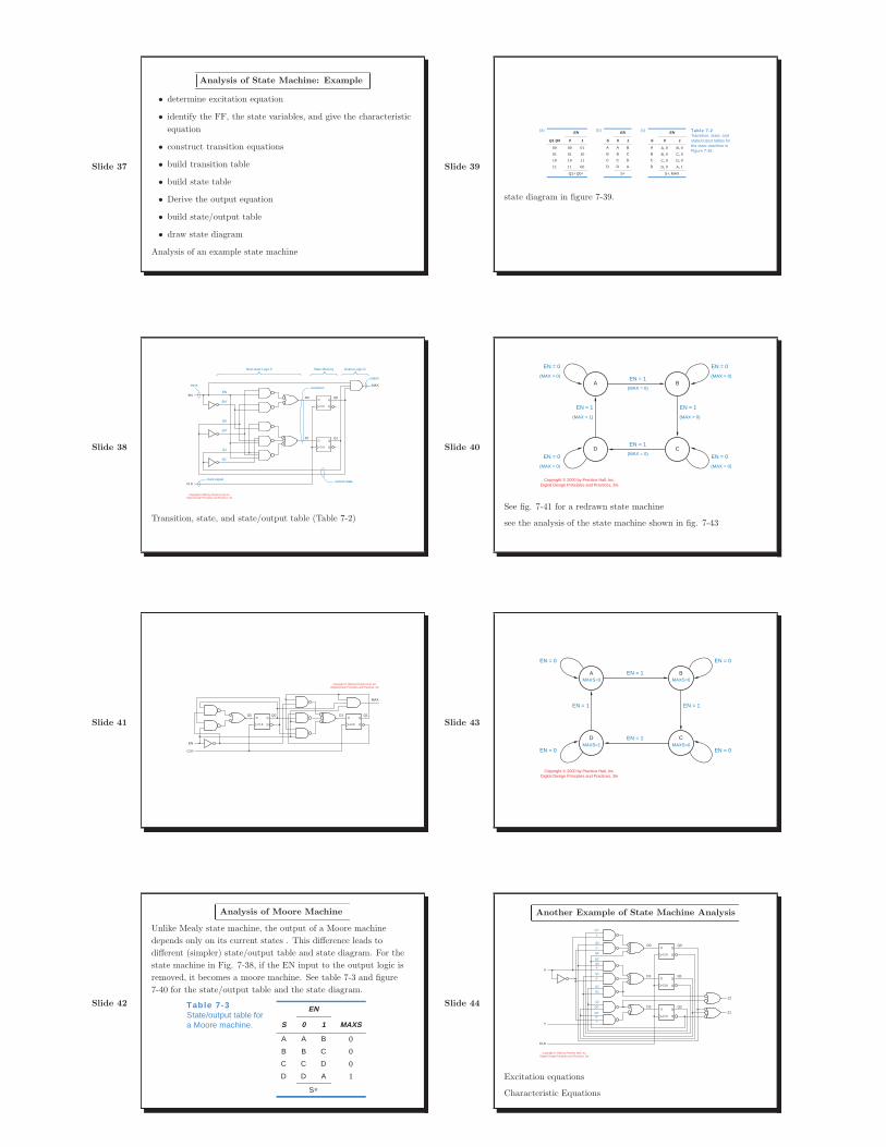
Slide 37
Analysis of State Machine: Example
• determine excitation equation
• identify the FF, the state variables, and give the characteristic
equation
• construct transition equations
• build transition table
• build state table
• Derive the output equation
• build state/output table
• draw state diagram
Analysis of an example state machine
Slide 38
EN
CLK
D0 Q0
D1 Q1
MAX
D Q
QCLK
D Q
QCLK
current state
excitation
output
input
clock signal
Next-state Logic F State Memory Output Logic G
EN′
EN
Q0′
Q0
Q1′
Q1
Copyright © 2000 by Prentice Hall, Inc. Digital Design Principles and Practices, 3/e
Transition, state, and state/output table (Table 7-2)
Slide 39
(a) EN (b) EN (c) EN Table 7-2Transition, state, and state/output tables for the state machine in Figure 7-38.
Q1 Q0 0 1 S 0 1 S 0 1
00 00 01 A A B A A, 0 B, 001 01 10 B B C B B, 0 C, 010 10 11 C C D C C, 0 D, 011 11 00 D D A D D, 0 A, 1
Q1∗ Q0∗ S∗ S∗, MAX
state diagram in figure 7-39.
Slide 40
A B
D C
EN = 1
(MAX = 0)
EN = 1
(MAX = 0)
EN = 1
(MAX = 0)
EN = 0
(MAX = 0)
EN = 0
(MAX = 0)
EN = 0
(MAX = 0)
EN = 0
(MAX = 0)
EN = 1
(MAX = 1)
Copyright © 2000 by Prentice Hall, Inc. Digital Design Principles and Practices, 3/e
See fig. 7-41 for a redrawn state machine
see the analysis of the state machine shown in fig. 7-43
Slide 41
EN
CLK
D0 Q0 D1 Q1
MAX
D Q
QCLK
D Q
QCLK
Copyright © 2000 by Prentice Hall, Inc. Digital Design Principles and Practices, 3/e
Slide 42
Analysis of Moore Machine
Unlike Mealy state machine, the output of a Moore machine
depends only on its current states . This difference leads to
different (simpler) state/output table and state diagram. For the
state machine in Fig. 7-38, if the EN input to the output logic is
removed, it becomes a moore machine. See table 7-3 and figure
7-40 for the state/output table and the state diagram.
Table 7-3State/output table for a Moore machine.
EN
S 0 1 MAXS
A A B 0B B C 0C C D 0D D A 1
S∗
Slide 43
A B
D C
EN = 1MAXS=0 MAXS=0
MAXS=1 MAXS=0EN = 1
EN = 1 EN = 1
EN = 0
EN = 0
EN = 0
EN = 0
Copyright © 2000 by Prentice Hall, Inc. Digital Design Principles and Practices, 3/e
Slide 44
Another Example of State Machine Analysis
Q0
Q1D1
D2 Q2
D Q
QCLK
D Q
QCLK
D0D Q
QCLK
Q0
Q0
Q0′
Q0′
Q1
Q1
Q1′
X
X′
X
Q2
Q2
Y
Q2′
Q2′
X′
X′
X
Y
CLK
Z2
Z1
Copyright © 2000 by Prentice Hall, Inc. Digital Design Principles and Practices, 3/e
Excitation equations
Characteristic Equations
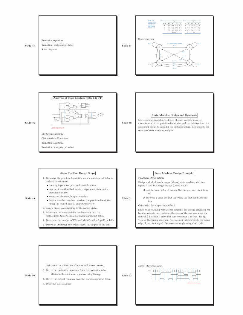
Slide 45
Transition equations
Transition, state/output table
State diagram
Slide 46
Analysis of State Machine with J-K FF
Q0
Q1
J0
K0
J1
K1
X
Y
CLK
Z
J Q
QK
CLK
J Q
QK
CLK
Q1
X
X
XQ0Q1Q0′Q1′YX
Y′
Y′
Y
Y
Y
Q0
Q0
Q0′
Copyright © 2000 by Prentice Hall, Inc. Digital Design Principles and Practices, 3/e
Excitation equations
Characteristic Equations
Transition equations
Transition, state/output table
Slide 47
Table 7-5Transition/output and state/output tables for the state machine in Figure 7-45.
(a) X Y (b) X Y
Q1 Q0 00 01 10 11 S 00 01 10 11
00 00, 0 10, 1 01, 0 10, 1 A A, 0 C, 1 B, 0 C, 101 01, 0 11, 0 10, 0 11, 0 B B, 0 D, 0 C, 0 D, 010 10, 0 00, 0 11, 0 00, 0 C C, 0 A, 0 D, 0 A, 011 11, 0 10, 0 00, 1 10, 1 D D, 0 C, 0 A, 1 C, 1
Q1∗ Q0∗, Z S ∗, Z
State Diagram
X′ • Y
X • Y
A B
C D
X • Y′
X • Y′
X • Y′
X • Y′
Y
X′ • Y′
X′ • Y′
X′ • Y′
X′ • Y′
YY
(Z = 1)
(Z = 1)
(Z = 1)
Z = 0 unless otherwise indicated
Slide 48
State Machine Design and Synthesis
Like combinational design, design of state machine involves
formalization of the problem description and the development of a
sequential circuit to solve for the stated problem. It represents the
reverse of state machine analysis.
Slide 49
State Machine Design Steps
1. Formalize the problem description with a state/output table or
with a state diagram
• identify inputs, outputs, and possible states
• represent the identified inputs, outputs,and states with
mnemonic names
• construct the state/output template
• instantiate the template based on the problem description
using the named inputs, output,and states.
2. Assign binary combinations to the named states
3. Substitute the state-variable combinations into the
state/output table to create a transition/output table.
4. Determine the number of FFs and identify a flip-flop (D or J-K)
5. Derive an excitation table that shows the output of the next
Slide 50
logic circuit as a function of inputs and current states.
6. Derive the excitation equations from the excitation table
Minimize the excitation equation using K-map
7. Derive the output equation from the transition/output table.
8. Draw the logic diagram
Slide 51
State Machine Design Example
Problem Description
Design a clocked synchronous (Moore) state machine with two
inputs A and B, a single output Z that is 1 if :
A had the same value at each of the two previous clock ticks,
or
B has been 1 since the last time that the first condition was
true
Otherwise, the output should be 0.
Since we are dealing with Moore machine, the second condition can
be alternatively interpreted as the state of the machine stays the
same if B has been 1 since last time condition 1 is true. See fig.
7-45 for the timing diagram. Note a clock tick represents the rising
edge of the clock signal. Between two neighboring clock ticks,
Slide 52
output stays the same.
CLOCK
A
B
Z
Copyright © 2000 by Prentice Hall, Inc. Digital Design Principles and Practices, 3/e
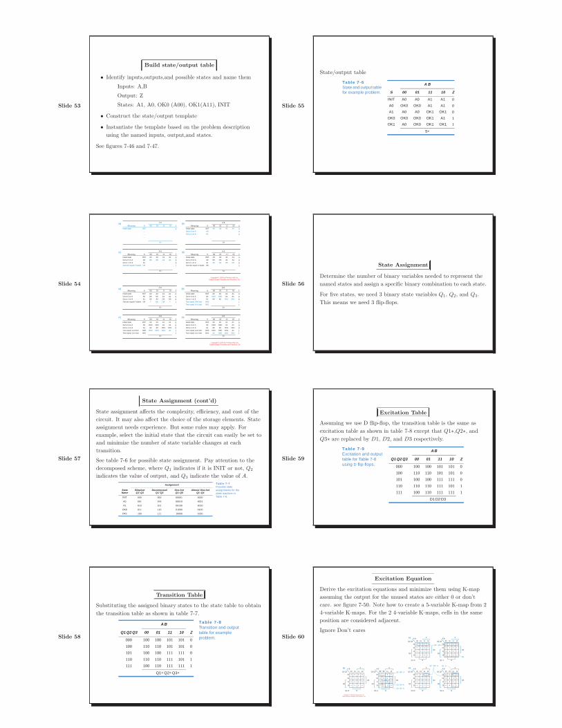
Slide 53
Build state/output table
• Identify inputs,outputs,and possible states and name them
Inputs: A,B
Output: Z
States: A1, A0, OK0 (A00), OK1(A11), INIT
• Construct the state/output template
• Instantiate the template based on the problem description
using the named inputs, output,and states.
See figures 7-46 and 7-47.
Slide 54
A1 A1 A0 A0 OK OK 0
0
00 S 01 11 10 Z
A B
S∗
INIT 00 S 01 11 10 Z
A B
S∗
INIT A0 A0 A1 A1 0A0A1
00 S 01 11 10 Z
A B
S∗
INIT A0 A0 A1 A1 0
0
A0 OK OK A1 A1 0
00 S 01 11 10 Z
A B
S∗
INIT A0 A0 A1 A1 0A0 OK OK A1 A1 0
0. . .. . .. . .
(a)
(c)
(b)
(d) Meaning
Initial stateGot a 0 on AGot a 1 on AGot two equal A inputs
MeaningInitial stateGot a 0 on AGot a 1 on AGot two equal A inputs
MeaningInitial stateGot a 0 on AGot a 1 on A
MeaningInitial state
OK OK01 1
Copyright © 2000 by Prentice Hall, Inc. Digital Design Principles and Practices, 3/e
0
00 S 01 11 10 Z
A B
S∗
INIT 00
OK1
(b) Meaning
Initial state
Two equal, A=1 last
A1 A0 A0 OK1 OK1
A0 A0 A1 A1A0 OK0 OK0 A1 A1Got a 0 on A
Got a 1 on ATwo equal, A=0 last OK0 1
1
A1 A0 A0 OK OK? OK OK ?
0
00 S 01 11 10 Z
A B
S∗
INIT A0 A0 A1 A1 0A0 OK OK A1 A1 0
(a) Meaning
Initial stateGot a 0 on AGot a 1 on AGot two equal A inputs OK 1
0
00 S Meaning 01 11 10 Z
A B(c)
S∗
INITInitial state 00
OK1Two equal, A=1 last
A1 A0 A0 OK1 OK1
A0 A0 A1 A1A0 OK0 OK0 A1 A1Got a 0 on A
Got a 1 on ATwo equal, A=0 last OK0 OK0 OK0 OK1 A1 1
1
0
00 S Meaning 01 11 10 Z
A B(d)
S∗
INITInitial state 00
A0 OK0 OK1 OK1OK1Two equal, A=1 last
A1 A0 A0 OK1 OK1
A0 A0 A1 A1A0 OK0 OK0 A1 A1Got a 0 on A
Got a 1 on ATwo equal, A=0 last OK0 OK0 OK0 OK1 A1 1
1
Copyright © 2000 by Prentice Hall, Inc. Digital Design Principles and Practices, 3/e
Slide 55
State/output table
Table 7 -6State and output table for example problem.
A B
S 00 01 11 10 Z
INIT A0 A0 A1 A1 0A0 OK0 OK0 A1 A1 0A1 A0 A0 OK1 OK1 0
OK0 OK0 OK0 OK1 A1 1OK1 A0 OK0 OK1 OK1 1
S∗
Slide 56
State Assignment
Determine the number of binary variables needed to represent the
named states and assign a specific binary combination to each state.
For five states, we need 3 binary state variables Q1, Q2, and Q3.
This means we need 3 flip-flops.
Slide 57
State Assignment (cont’d)
State assignment affects the complexity, efficiency, and cost of the
circuit. It may also affect the choice of the storage elements. State
assignment needs experience. But some rules may apply. For
example, select the initial state that the circuit can easily be set to
and minimize the number of state variable changes at each
transition.
See table 7-6 for possible state assignment. Pay attention to the
decomposed scheme, where Q1 indicates if it is INIT or not, Q2
indicates the value of output, and Q3 indicate the value of A.
Assignment Table 7-7Possible state assignments for the state machine in Table 7-6.
State Name
Simplest Q1–Q3
Decomposed Q1–Q3
One-hot Q1–Q5
Almost One-hot Q1–Q4
INIT 000 000 00001 0000A0 001 100 00010 0001A1 010 101 00100 0010
OK0 011 110 01000 0100OK1 100 111 10000 1000
Slide 58
Transition Table
Substituting the assigned binary states to the state table to obtain
the transition table as shown in table 7-7.
A B Table 7-8Transition and output table for example problem.
Q1 Q2 Q3 00 01 11 10 Z
000 100 100 101 101 0100 110 110 101 101 0101 100 100 111 111 0110 110 110 111 101 1111 100 110 111 111 1
Q1∗ Q2∗ Q3∗
Slide 59
Excitation Table
Assuming we use D flip-flop, the transition table is the same as
excitation table as shown in table 7-8 except that Q1∗,Q2∗, and
Q3∗ are replaced by D1, D2, and D3 respectively.
Table 7-9Excitation and output table for Table 7-8 using D flip-flops.
A B
Q1 Q2 Q3 00 01 11 10 Z
000 100 100 101 101 0100 110 110 101 101 0101 100 100 111 111 0110 110 110 111 101 1111 100 110 111 111 1
D1 D2 D3
Slide 60
Excitation Equation
Derive the excitation equations and minimize them using K-map
assuming the output for the unused states are either 0 or don’t
care. see figure 7-50. Note how to create a 5-variable K-map from 2
4-variable K-maps. For the 2 4-variable K-maps, cells in the same
position are considered adjacent.
Ignore Don’t cares
00 01 11 10
00
01
11
10
00 01 11 10A B
Q2 Q3
00
01
11
10
A
B
A BA
B
A BA
B
A BA
B
A BA
B
A BA
B
Q2
Q3
Q1=0
Q2 Q3
Q2
Q3
Q1=1
10
00
01
11
10
00 01 11 10Q2 Q3
00
01
11
10Q2
Q3
Q1=0
Q2 Q3
Q2
Q3
Q1=1
00 01 11 10
00
01
11
10
00 01 11 10Q2 Q3
00
01
11
10Q2
Q3
Q1=0
Q2 Q3
Q2
Q3
Q1=1
D1
D2 D3
1
0 0 0 0
0 0 0 0
0 0 0 0
0 0 0 0
0 0 0 0
0 0 0 0
0 0 0 0
0 0 0 0
0 0 0 0
1 1 1
0 0 0 0
1 1 1 1
1 1 1 1
1 1 1 1
1 1 1 1
1 1 0 0
0 0 1 1
0 1 1 1
0 1 1
0 1 1
0 1 1
0 1
0
0
0
0 1
0 1 10
1 1 1 0
Q1
00 11 Q1 • Q3′ • A′
Q1 • Q3 • A
Q1 • Q2 • B
Q1 • AQ2′ • Q3′ • A
01
Q2′ • Q3′
Copyright © 2000 by Prentice Hall, Inc. Digital Design Principles and Practices, 3/e
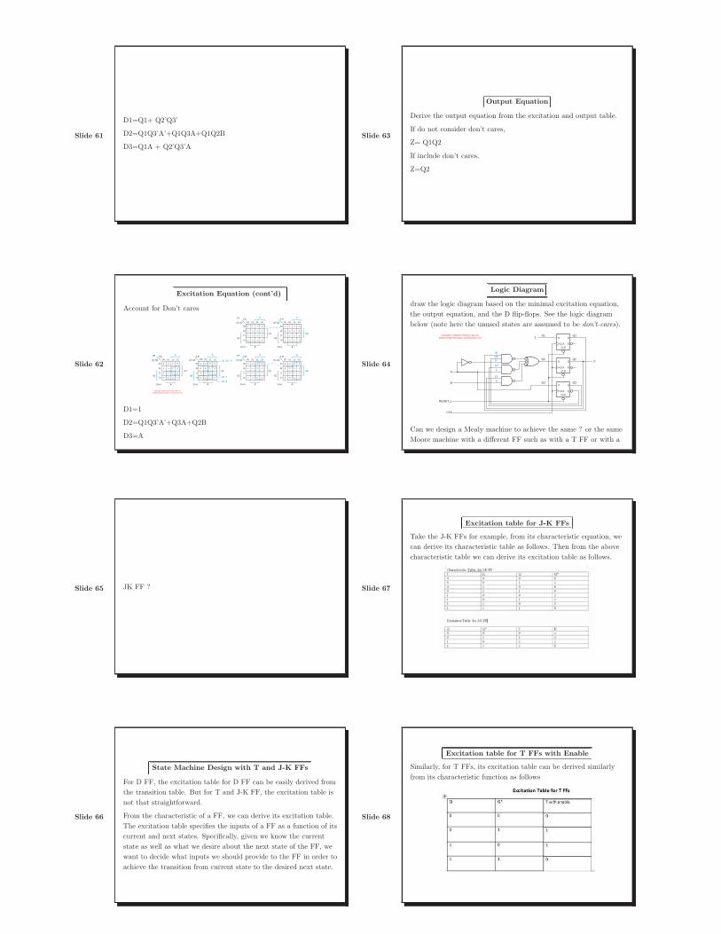
Slide 61
D1=Q1+ Q2’Q3’
D2=Q1Q3’A’+Q1Q3A+Q1Q2B
D3=Q1A + Q2’Q3’A
Slide 62
Excitation Equation (cont’d)
Account for Don’t cares
00 01 11 10
00
01
11
10
00 01 11 10A B
Q2 Q3
00
01
11
10
A
B
A BA
B
A BA
B
A BA
B
A BA
B
A BA
B
Q2
Q3
Q1=0
Q2 Q3
Q2
Q3
Q1=1
10
00
01
11
10
00 01 11 10Q2 Q3
00
01
11
10Q2
Q3
Q1=0
Q2 Q3
Q2
Q3
Q1=1
00 01 11 10
00
01
11
10
00 01 11 10Q2 Q3
00
01
11
10Q2
Q3
Q1=0
Q2 Q3
Q2
Q3
Q1=1
D1
D2 D3
1 1 1 1
0 0 0 0
1 1 1 1
1 1 1 1
1 1 1 1
1 1 1 1
1 1 0 0
0 0 1 1
0 1 1 1
0 11
0 11
0 11
0 1
0
0
0
0 1
0
d d d d
d d d d
d d d d
d d d d
d d d d
d d d d
d d d d
d d d d
d d d d
0 1 1
1 1 1 0
1
00 11 Q1 • Q3′ • A′
Q3 • A
Q2 • B
A
01
Copyright © 2000 by Prentice Hall, Inc. Digital Design Principles and Practices, 3/e
D1=1
D2=Q1Q3’A’+Q3A+Q2B
D3=A
Slide 63
Output Equation
Derive the output equation from the excitation and output table.
If do not consider don’t cares,
Z= Q1Q2
If include don’t cares,
Z=Q2
Slide 64
Logic Diagram
draw the logic diagram based on the minimal excitation equation,
the output equation, and the D flip-flops. See the logic diagram
below (note here the unused states are assumed to be don’t-cares).
Q1
Q2D2
D3 Q3
D1D Q
QCLKCLR
D Q
QCLKCLR
D Q
QCLKCLR
Q3′A′
Q1
Q3
A
Q2
B
A
B
CLK
RESET_L
1
Z
Copyright © 2000 by Prentice Hall, Inc. Digital Design Principles and Practices, 3/e
Can we design a Mealy machine to achieve the same ? or the same
Moore machine with a different FF such as with a T FF or with a
Slide 65 JK FF ?
Slide 66
State Machine Design with T and J-K FFs
For D FF, the excitation table for D FF can be easily derived from
the transition table. But for T and J-K FF, the excitation table is
not that straightforward.
From the characteristic of a FF, we can derive its excitation table.
The excitation table specifies the inputs of a FF as a function of its
current and next states. Specifically, given we know the current
state as well as what we desire about the next state of the FF, we
want to decide what inputs we should provide to the FF in order to
achieve the transition from current state to the desired next state.
Slide 67
Excitation table for J-K FFs
Take the J-K FFs for example, from its characteristic equation, we
can derive its characteristic table as follows. Then from the above
characteristic table we can derive its excitation table as follows.
Slide 68
Excitation table for T FFs with Enable
Similarly, for T FFs, its excitation table can be derived similarly
from its characteristic function as follows

Slide 69
Excitation Table for D, T with EN, and JK FF
Given the excitation table, show how to construct a T FF (or T FF
with enable from a D FF or JK FF)?
Slide 70
Excitation Table with J-K FF
Change the transition table (table 7-8) to the following format
Complete the excitation table using the transition table by
transferring the numbers in table 7-8 to and the J-K excitation
table. We can then easily derive the excitation equations from the
table.
Slide 71 Note such a format of excitation table applies to all FFs.
Slide 72
Sequential Circuit Design Example
Problem:
Design a Moore state machine that accepts an input binary
sequence such as 001010011101 .... Its output is zero except when
the number of 1’s that have been input is a multiple of three.
Implement the machine using as few as flip-flops as possible.
Steps: state/output table, transition table, excitation table,
minimized excitation equations, minimized output equations, and
diagram.
Slide 73
Input, output, States
• Input: X
• Output: Z
• States:
– INIT-inital state
– S0-the number of 1’s is multiple of 3
– S1-the number of 1’s is 1 in excess of multiple of 3
– S2-the number of 1’s is 2 in excess of multiple of 3
Implement this state machine using D, T, and J-K FFs respectively.
Slide 74
State Machine Design using State Diagrams
State machine design with state diagram presents a graphical
design approach. It is more intuitively appealing. Caution,
however, must be exercised while using state diagrams since the
constructed state diagram may be ambiguous.
Slide 75
Word Problem 1
Design a circuit that detects an input sequence of 101 and that
allows overlaps. The circuit can be a Moore or a Mealy machine.
Steps: state diagram, state/output table, transition table,
excitation table, minimized excitation equations, minimized output
equations, and diagram. Implement it using one D FF and one JK
FF.
Slide 76
Word Problem 2
Design a sequential circuit that has one input (X) and one output
(Z). The circuit examines groups of three consecutive inputs and
produces an output. The output is Z=1 if the input sequence 1011
occurs.
• Draw the state diagram
• Give the state/output table
design it as a Moore and Mealy machine ? what is the difference ?
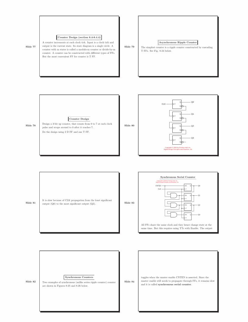
Slide 77
Counter Design (section 8.4-8.4.4)
A counter increments at each clock tick. Input is a clock tick and
output is the current state. Its state diagram is a single circle. A
counter with m states is called a modulo-m counter or divide-by-m
counter. A counter can be constructed with different types of FFs.
But the most convenient FF for counter is T FF.
Slide 78
Counter Design
Design a 3-bit up counter, that counts from 0 to 7 at each clock
pulse and wraps around to 0 after it reaches 7.
Do the design using 2 D FF and one T FF.
Slide 79
Asynchronous Ripple Counter
The simplest counter is a ripple counter constructed by cascading
T FFs. See Fig. 8-24 below.
Slide 80
Q
QTCLK
T
T
T
Q0
Q1
Q2
Q3
Q
Q
Q
Q
Q
Q
Copyright © 2000 by Prentice Hall, Inc. Digital Design Principles and Practices, 3/e
Slide 81
It is slow because of CLK propagation from the least significant
output (Q0) to the most significant output (Q3).
Slide 82
Synchronous Counters
Two examples of synchronous (unlike series ripple counter) counter
are shown in Figures 8-25 and 8-26 below.
Slide 83
Synchronous Serial Counter
Q
T
EN
CLK
CNTEN
Q
T
Q
T
Q
T
Q0
Q1
Q2
Q3
EN
EN
EN
Copyright © 2000 by Prentice Hall, Inc. Digital Design Principles and Practices, 3/e
All FFs share the same clock and they hence change state at the
same time. But this requires using TTs with Enable. The output
Slide 84
toggles when the master enable CNTEN is asserted. Since the
master enable still needs to propagate through FFs, it remains slow
and it is called synchronous serial counter.
Slide 85
Synchronous Parallel Counter
Q
T
EN
CLK
CNTEN
Q
T
Q
T
Q
T
Q0
Q1
Q2
Q3
EN
EN
EN
Copyright © 2000 by Prentice Hall, Inc. Digital Design Principles and Practices, 3/e
All FF share the same CLK and Enable. There are no delay. It is
the fastest binary counter.
Slide 86
MSI Counter Chip
The most popular MSI counter is 74 x 163.
74x163
CLRCLK
LD
QAQB
2
14
11
1
9
ENPENT
7
10
AB
3
4
CD
5
6QCQD
15RCO
13
12
Copyright © 2000 by Prentice Hall, Inc. Digital Design Principles and Practices, 3/e
Slide 87
It is a 4-bit up counter, with clear (CLR) and load (LD) inputs,
two enable inputs (ENP,ENT), and ripper carry-output (RCO).
Slide 88
MSI Counter Chip (cont’d)
Table 8-11 State table for a 74x163 4-bit binary counter.
Inputs Current State Next State
CLR_L LD_L ENT ENP QD QC QB QA QD∗ QC∗ QB∗ QA∗
0 x x x x x x x 0 0 0 01 0 x x x x x x D C B A
1 1 0 x x x x x QD QC QB QA
1 1 x 0 x x x x QD QC QB QA
1 1 1 1 0 0 0 0 0 0 0 1 1 1 1 1 0 0 0 1 0 0 1 0 1 1 1 1 0 0 1 0 0 0 1 1 1 1 1 1 0 0 1 1 0 1 0 0 1 1 1 1 0 1 0 0 0 1 0 1 1 1 1 1 0 1 0 1 0 1 1 0 1 1 1 1 0 1 1 0 0 1 1 1 1 1 1 1 0 1 1 1 1 0 0 0 1 1 1 1 1 0 0 0 1 0 0 1 1 1 1 1 1 0 0 1 1 0 1 0 1 1 1 1 1 0 1 0 1 0 1 1 1 1 1 1 1 0 1 1 1 1 0 0 1 1 1 1 1 1 0 0 1 1 0 1 1 1 1 1 1 1 0 1 1 1 1 0 1 1 1 1 1 1 1 0 1 1 1 1 1 1 1 1 1 1 1 1 0 0 0 0
Slide 89
MSI Counter Chip (cont’d)
The output is 0 if CLR is asserted. The output is A,B,C,D if LD is
asserted. If either ENP os ENT is asserted, the output stays the
same as the last state. RCO is asserted if all four outputs are 1.
Slide 90
Module-11 Counter
74x163 can be used to build different counters (see Fig. 8-29).
The following is an module-11 decimal counter (i.e., count up to 11
and wrap around) built with 74x16374x163
74x00
CLRCLK
LD
QAQB
2
14
11
1
1
2
9
ENPENT
7
10
A Q0Q1Q2Q3
BCD
QCQD
15
3
RCO
13
12
S11XX_L
U1U2
+5 V
CLOCK
RPUR3
4
5
6
Copyright © 2000 by Prentice Hall, Inc. Digital Design Principles and Practices, 3/e
When Q2=Q3=1, through the NAND gate, LD is asserted, the
Slide 91 values A,B,C,and D (they are 1100) are loaded into the output.
Slide 92
More State Machine Design Example
Design a state machine with two inputs X and Y, and output Z.
The output is 1 if the number of 1 inputs on X and Y since reset is
a multiple of 4.
See section 7.4.6 for details.

Slide 93
State Design: Another Example
Design a controller for T-bird tail lights.
ZOTTFFSCALIFORNIA
RA RB RCLC LB LA
Copyright © 2000 by Prentice Hall, Inc. Digital Design Principles and Practices, 3/e
Slide 94
Problem statement: three lights on each side, and for turn, they
operate in sequence to show the turning direction
LC(a) LB LA RA(b) RB RC
Copyright © 2000 by Prentice Hall, Inc. Digital Design Principles and Practices, 3/e
It has three inputs: Left, Right, and Haz. The left (right) lights are
Slide 95
on when the Left (Right) input is on and six lights all flash when
the HAZ is on. Assume the clock frequency matches the light flash
rate.
Slide 96
T-bird tail light design
Input: left, right, haze
output: six lights: 3 for left (LA, LB, LC) and 3 for right (RA, RB,
RC)
States: IDLE, L1, L2, L3, R1, R2, R3, LR3
see progressive improvement in state diagrams from Fig. 7.56, 7.57,
and 7.58.
Slide 97LR3
R1R3
R2
IDLE
L1
L2
LEFT • HAZ′ • RIGHT′
1
1
RIGHT • HAZ′ • LEFT′1
HAZ′ HAZ′ HAZ
HAZ + LEFT • RIGHT
L3
(LEFT + RIGHT + HAZ)′
HAZ′ HAZ′ HAZ
HAZ
HAZ
Slide 98
Transition List
From the constructed state diagram, we can build a transition list
table as shown in Table 7-14. Transition equations can be directly
derived from the transition list. The transition equation for a next
state is the sum of transition expression for which the next state
variable has a value of 1. Transition equation can then be
simplified algebraically or using K-map. Excitation equations can
be derived from transition equations.
Slide 99
S Q2 Q1 Q0 Transition Expression S∗ Q2∗ Q1∗ Q0∗ Table 7-17Transition list for T-bird tail-lights state machine.
IDLE 0 0 0 (LEFT + RIGHT + HAZ)′ IDLE 0 0 0
IDLE 0 0 0 LEFT ⋅ HAZ′ ⋅ RIGHT′ L1 0 0 1
IDLE 0 0 0 HAZ + LEFT ⋅ RIGHT LR3 1 0 0
IDLE 0 0 0 RIGHT ⋅ HAZ′ ⋅ LEFT′ R1 1 0 1
L1 0 0 1 HAZ′ L2 0 1 1
L1 0 0 1 HAZ LR3 1 0 0
L2 0 1 1 HAZ′ L3 0 1 0
L2 0 1 1 HAZ LR3 1 0 0
L3 0 1 0 1 IDLE 0 0 0
R1 1 0 1 HAZ′ R2 1 1 1
R1 1 0 1 HAZ LR3 1 0 0
R2 1 1 1 HAZ′ R3 1 1 0
R2 1 1 1 HAZ LR3 1 0 0
R3 1 1 0 1 IDLE 0 0 0
LR3 1 0 0 1 IDLE 0 0 0

Slide 1
Chapter 8 Sequential Logic Design Practices
• Registers (section 8.2.5)
• Shift Registers (section 8.5.1-8.5.2)
• Counters (section 8.4)
Slide 2
Registers
A register is a storage device, consisting of a collection of D FFs
with a common clock input. Each D FF can store 1 bit of data.
74x175 is a 4-bit register.
Slide 3
74x175
CLRCLK
1D1Q
9
2
1Q3
1
4
2D5
3D12
4D13
2Q7
6
3Q10
11
4Q
2Q
3Q
4Q
15
14
(b)
(a)
D Q
QCLK
CLR
(2)
(3)
(4)1Q
1Q_L
1D
D Q
QCLK
CLR
(7)
(6)
(5)2Q
2Q_L
2D
D Q
QCLK
CLR
(10)
(11)
(12)3Q
3Q_L
3D
D Q
QCLK
CLR
(15)
(14)
(13)
(9)
(1)
4Q
4Q_L
4D
CLK
CLR_L
Copyright © 2000 by Prentice Hall, Inc. Digital Design Principles and Practices, 3/e
The data inputs (1D-4D) are transferred to the D FFs (transferring
to Q1-Q4) at each clock tick. It includes a synchronous clear input,
which clears the FFs (i.e., set the Qs to zero) if asserted.
74x374 is a 8-bit register. See Figure 8-10.
Slide 4
Shift Registers
A shift register shifts its stored data by one bit position at each
clock tick. There are four types of shift registers: serial-in, serial
out; serial-in, parallel-out; parallel-in, serial-out, and and
parallel-in, parallel-out.
Go to Wikipedia at http://en.wikipedia.org/wiki/Shift register for
a demo of each register.
Slide 5
Serial-in Serial-Out Shift Registers
The input data SERIN is applied sequentially to the D input of the
first FF. During each clock pulse, one bit is transmitted from
current FF to next FF. The output is read one bit at a time from
the last FF.
Slide 6
Q
CLOCK
SERIN
CK
CK
D
D
SEROUT
Q
QD
CK
Copyright © 2000 by Prentice Hall, Inc. Digital Design Principles and Practices, 3/e
Slide 7
Serial-in Parallel-Out Shift Registers
The input data SERIN is applied sequentially to the D input of the
first FF. During each clock pulse, one bit is transmitted from
current FF to next FF. The output is read simultaneously from all
FFs.
Slide 8
1Q
2Q
NQ
Q
CLOCK
SERIN
CK
CK
D
D Q
QD
CK
Copyright © 2000 by Prentice Hall, Inc. Digital Design Principles and Practices, 3/e
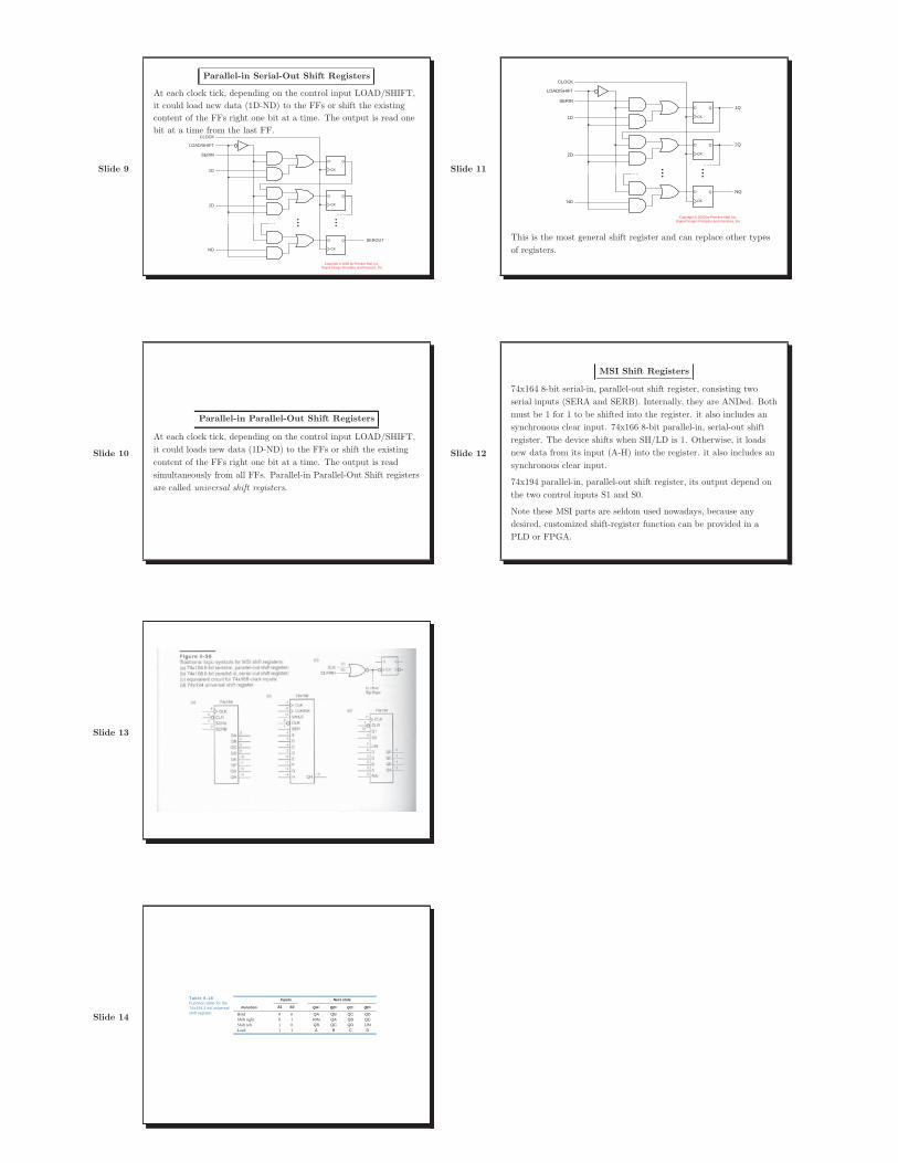
Slide 9
Parallel-in Serial-Out Shift Registers
At each clock tick, depending on the control input LOAD/SHIFT,
it could load new data (1D-ND) to the FFs or shift the existing
content of the FFs right one bit at a time. The output is read one
bit at a time from the last FF.
Q
CLOCK
LOAD/SHIFT
SERIN
CK
D
SEROUT
1D
Q
CK
D
2D
Q
CK
D
ND
Copyright © 2000 by Prentice Hall, Inc. Digital Design Principles and Practices, 3/e
Slide 10
Parallel-in Parallel-Out Shift Registers
At each clock tick, depending on the control input LOAD/SHIFT,
it could loads new data (1D-ND) to the FFs or shift the existing
content of the FFs right one bit at a time. The output is read
simultaneously from all FFs. Parallel-in Parallel-Out Shift registers
are called universal shift registers.
Slide 11
Q
CLOCK
LOAD/SHIFT
SERIN
CK
D
NQ
1Q
2Q
1D
Q
CK
D
2D
Q
CK
D
ND
Copyright © 2000 by Prentice Hall, Inc. Digital Design Principles and Practices, 3/e
This is the most general shift register and can replace other types
of registers.
Slide 12
MSI Shift Registers
74x164 8-bit serial-in, parallel-out shift register, consisting two
serial inputs (SERA and SERB). Internally, they are ANDed. Both
must be 1 for 1 to be shifted into the register. it also includes an
synchronous clear input. 74x166 8-bit parallel-in, serial-out shift
register. The device shifts when SH/LD is 1. Otherwise, it loads
new data from its input (A-H) into the register. it also includes an
synchronous clear input.
74x194 parallel-in, parallel-out shift register, its output depend on
the two control inputs S1 and S0.
Note these MSI parts are seldom used nowadays, because any
desired, customized shift-register function can be provided in a
PLD or FPGA.
Slide 13
Slide 14
Table 8-18Function table for the 74x194 4-bit universal shift register.
Inputs Next state
Function S1 S0 QA∗ QB∗ QC∗ QD∗Hold 0 0 QA QB QC QDShift right 0 1 RIN QA QB QCShift left 1 0 QB QC QD LINLoad 1 1 A B C D
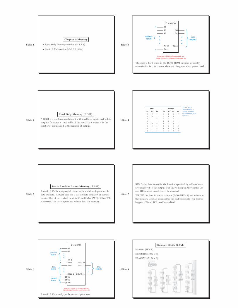
Slide 1
Chapter 9 Memory
• Read-Only Memory (section 9.1-9.1.1)
• Static RAM (section 9.3-9.3.2, 9.3.4)
Slide 2
Read Only Memory (ROM)
A ROM is a combinational circuit with n address inputs and b data
outputs. It stores a truth table of the size 2n x b, where n is the
number of input and b is the number of output.
Slide 3
2n × b ROM
A0A1 D0A2 D1
An–2 Db–1An–1
addressinputs
dataoutputs
Copyright © 2000 by Prentice Hall, Inc. Digital Design Principles and Practices, 3/e
The data is hard-wired in the ROM. ROM memory is usually
non-volatile, i.e., its content does not disappear when power is off.
Slide 4
Inputs Outputs Table 10-1Truth table for a 3-input, 4-output combinational logic function.
A2 A1 A0 D3 D2 D1 D0
0 0 0 1 1 1 00 0 1 1 1 0 10 1 0 1 0 1 10 1 1 0 1 1 11 0 0 0 0 0 11 0 1 0 0 1 01 1 0 0 1 0 01 1 1 1 0 0 0
Slide 5
Static Random Access Memory (RAM)
A static RAM is a sequential circuit with n address inputs and b
data outputs. A RAM also has b data inputs and a set of control
inputs. One of the control input is Write-Enable (WE). When WE
is asserted, the data inputs are written into the memory.
Slide 6
2n × b RAM
A0A1
DOUT0DOUT1
An–1
addressinputs
DIN0DIN1
DINb–1 DOUTb–1CSOEWE
datainputs
dataoutputs
controlinputs
Copyright © 2000 by Prentice Hall, Inc. Digital Design Principles and Practices, 3/e
A static RAM usually performs two operations.
Slide 7
READ–the data stored in the location specified by address input
are transfered to the output. For this to happen, the eanbles CS
and OE (output enable) need be asserted.
WRITE-the data in the data input (DIN0-DINb-1) are written to
the memory location specified by the address inputs. For this to
happen, CS and WE need be enabled.
Slide 8
Standard Static RAMs
HM6284 (8k x 8)
HM628128 (128k x 8)
HM628512 (512k x 8)
1
Advanced Topics
•Fundam
entals in Com
puter O
rganization•
Introduction to VHD
L
2
Register
Register
Data In
(N bits)
Load
Data O
ut(N
bits)
Output Enable
NN
(we have Tri-state outputs)
Basic B
uilding Blocks (1)
3
Basic B
uilding Blocks (2)
ShiftR
egister
Data In
Load
Data O
ut
Output Enable
NN
Shift Controls
(left/right/no shift)
Shift Register
4
Basic B
uilding Blocks (4)
Arithm
etic-Logic Unit
NN
AB
ALU
Operation
N
Flags(carry out, overflow
, etc.)R
esult
Keep in m
ind:
The ALU
is a com
binationalcircuit.
5
Buses
Data Lines (tw
o-way)
N
Address Lines (one-way)
M
Control Lines (m
ix of 1 and 2-way lines)
C
Ashared
collection of wires for exchanging data, w
ith some defined rules
Rule 1:O
nly one device can write
to a bus at any time
Rule 2:M
ultiple devices can readthe bus at any tim
eR
ule 3:There is usually a bus protocolthat is followed
strictly by all devices sharing the bus
6
3 Registers Sharing a B
usNMC
Register 1
Register 2
Register 3
OE1
OE2
OE3
LOAD
1LO
AD2
LOAD
3
Only one of
these OE’s
can be true at once
Several of thesecan be true
at once for input
OE’s and
LOAD
’sgenerally
determined
by the control lines
To write, O
E must be enabled. To read,
LOAD
must be enabled.
Only
one canw
rite to the data
line
7
Register-to-R
egister Data Transfer
N
OE1
MC
Register 1
Register 2
Register 3
OE2
OE3
LOAD
1LO
AD2
LOAD
3
Register 1
Register 3
Only one can w
rite to the data line, but more than one
registers can receive inputs at the same tim
e8
Buses &
Registers to R
AM
Random
AccessM
emory
MAR
Mem
oryAddressR
egister(store address here)
MBR
Mem
oryB
ufferR
egister(exchange data here)
Request (C
hip Select)R
ead/Write
Wait
Mem
oryC
ontrolSignalsSlow
RAM
susually ask
Processor to wait
9
Note: This is not the only
way to build a com
puter,but is the m
ost comm
on one.
I want to build a com
puter!B
asic Idea #1: The Stored Program C
omputer C
oncept
This is an instruction-controlled digital system w
ith a mem
ory
A sequence of instructionsare stored in m
emory
This set of instructions constitute the programthat defines the
machine’s behavior
The same m
emory also holds the data
needed to executethe
program
The same m
emory also holds the outputs
produced by the program
, as well as any interm
ediate results
The mem
ory is large (ideally, infinite)
10
The processor executes the following “infinite loop” forever:
Step 1. Fetch the next instructionfrom
mem
ory to a registerThe register is usually called the instruction register (IR
).The address of the next instruction is usually
stored in a register called the program counter (PC
).So, Fetch does the follow
ing: 1) get the instruction address from
PC; 2) read the instruction from
them
emory; 3) transfer the instruction to IR
.Step 2. D
ecodethe instruction
Step 3. Fetch any operandsneeded
Step 4. Executethe instruction
Step 5. Do internal housekeeping, and G
o to Step 1O
ne important chore is to change the address in the
PCto point to the next instruction.
The Cycle of Life
Basic Idea #2: The Instruction C
ycle
11
Structure of a Com
puterProcessor
Mem
orySystem
Control
Datapath
AddressR
ead/Write
Data
Control
Signals
Data
Inputs
The Datapath U
nit, also called the execution unit, consisting of R
egisters for temporary data storage and functional unit to
perform operation on the data. M
ain parts: Registers, Shifter, ALU
, Buses.
The Control U
nit, also called the instruction unit. It provides instruction as to w
hat operation to performM
ainparts:Finite-State
Machine
updatePC
(sinceinputs
The Processor consists of tw
o m
ajorparts:
Central
ProcessingU
nit(C
PU)
In its sim
plest form
, a com
puter consists of a processor(C
PU) and
am
emory
system.
12
TheB
US
is likea highw
ay fortransferring data from
one point to any other point
Program C
ounter(H
olds address of N
EXT instruction)Instruction R
egister(H
olds the fetchedinstruction)
Accumulator
Involved in most
instructions
Note that this one
has two outputs
Put Them Together!
Single Bus D
esign
The Datapath U
nit
Mem
oryA
ddressB
usM
emory
Data B
usMAR
PCIR
AC
AB
MBR
BU
S
ALU
13
Note, the B
US
Note, the B
US
is treated just like a register
Register Transfer O
perations
Register transfer operations:
PC
BU
SIR
BU
SAC
B
US
MB
R
BU
SALU
Result
BU
S
BU
S PC
BU
S IR
BU
S AC
BU
S M
BR
BU
S ALU
BB
US
MAR
AC
ALU A
(hardwired)
Mem
oryA
ddressB
usM
emory
Data B
usMAR
PCIR
AC
AB
MBR
BU
SSingle B
us Design
They all share one bus.14
More R
ealistic Datapath U
nitThree B
us Design —
Supports more parallelism
Single bus replaced by three busses:M
emory B
us (MB
US)
Result B
us (RB
US)
Address Bus (AB
US)
Mem
ory Bus (M
BU
S)R
esult Bus (R
BU
S)Address B
us (ABU
S)
Address B
us
MAR
PCIR
Mem
oryA
ddressB
usAC
AB
MBR
Result B
us
Mem
ory Bus
Mem
oryD
ata Bus
15
We sim
plified our datapath further by assuming that M
BR
is inside the m
emory system
itself and MB
US has tw
o branches.
Add M
emory
Every device in this diagram has control signals that m
ust be operated.
RB
US
ACM
BU
S
AB
ALU
Mem
oryN
bits wide
2M
words
MAR
S
PCIR
MB
US
Mem
oryAddressAB
US
16
Add C
ontrolACA
B
ALUM
ARS
PC
FSM
IR
Mem
oryAddress
Opcode
The control unit is a finite state m
achine (FSM).
Every bit of the Instruction R
egister(IR), every other
register’s OE and LO
AD
signals, every control input and flag output of the ALU
, and every m
emory control
signal is either an input or an output of the control unit.(Show
n in red)
3 for ALU, 1 each for, M
AR,
and PC.
Reality N
ote #1:The control unit FSM is huge com
pared to the FSM
examples that w
e’ve seen thus far!!
Reality N
ote #2: The diagram above is extrem
ely sim
plified compared to a real processor
Control Flow
Data Flow
RB
USM
BU
S
Mem
oryN
bits wide
2M
words
MB
US
ABU
S

17
How
does it work? (1)
3. Operand Fetch:
Move operand address from
IR to M
ARInitiate a m
emory read sequence
Store Path
ACLoad Path
AB
ALU
Mem
oryN
bits wide
2M
words
MAR
S
PC
FSM
IR
Instruction Path
Mem
oryAddress
Opcode
OPC
OD
EO
PERAN
DSPEC
IFIER
Instruction Format
Let's trace an instruction: AC
AC
+ Mem
<address>
1. Instruction Fetch:M
ove PC to M
ARInitiate a m
emory read sequence
Move data from
mem
ory to IR
2. Instruction Decode:
Opcode bits of IR
are input to control FSMR
est of IR bits encode the
operand address (see Fig 11.4)
18
How
does it work? (2)
Store Path
ACLoad Path
AB
ALU
Mem
oryN
bits wide
2M
words
MAR
S
PC
FSM
IR
Instruction Path
Mem
oryAddress
Opcode
OPC
OD
EO
PERAN
DSPEC
IFIER
Instruction Format
4. Instruction Execute:D
ata available on load pathM
ove data to ALU input
Configure ALU
to perform AD
D
operationM
ove result S to AC
5. Housekeeping:
Update PC
to point at next instruction
Let us trace an instruction: AC
AC
+ Mem
<address>
19
The Control U
nitW
hat the Control unit is doing:
Transfers data from one register to another
Asserts appropriate control signals
We can think about the control unit m
ost easilyin term
s of a series ofregister transfers andm
icrooperations, using a program
ming-like notation
Register transfer notation -A w
ay to represent the detailedim
plementation of register transfer operations
Micro-operations-detailed operations for each register transfer
Notation.
20
Register to R
egister moves
Register Transfer N
otationInstruction fetch:
PC
MAR
;--m
ove PC to M
ARM
emory R
ead;--assert M
emory R
EAD signal
Mem
ory IR
;--load IR
from M
emory
Instruction Decode:
IF IR<op code> = AD
D_FR
OM
_MEM
ORY
THEN
Instruction Execution:M
emory
ALU B
;--gate M
emory to ALU
BAC
ALU
A;--gate AC
to ALU A
ALU AD
D;
--instruct ALU to perform
ADD
ALU S
AC;
--gate ALU result to AC
Assert Control
Signal
Operand fetch:
IR<addr>
MAR
;--m
ove operand addr to MAR
Mem
ory Read;
--assert Mem
ory READ
signal
Housekeeping:
PC+1
PC;
--increment PC
Repeat the five steps !
21
Micro-O
perations
Instruction fetch:PC
AB
US;
ABU
S M
AR;
1R
ead/Write*;
MB
R
MB
US;
MB
US
IR;
Instruction Decode:
IF IR<O
pCode> = LO
AD_FR
OM
_MEM
ORY
THEN
Instruction Execution:M
BR
M
BU
S;M
BU
S ALU
B;
ALU PASS B
;ALU
Result
RB
US;
RB
US
AC;
Operand fetch:
IR-> AB
US
ABU
S->MA
R1
Read/W
rite*;
Housekeeping:
PC+1
PC;
Instruction Fetch
22
Micro-operations
One register transfer operation m
ay be several micro-operations
Some operations are directly im
plemented by functional units:
e.g., ADD
, Pass B, 0
PC, PC
+ 1 PC
Some others require m
ultiple control operations:
e.g., PCM
ARim
plemented as PC
ABU
Sand
ABU
S M
AR
See page 588
23
Interrupts, Resets
24
Example Task
Read the output of the 4-bit data source every tim
e the push button is pressed, and display the result.
4-bit D
ataSource
Push Button
Com
puter(H
C11 chip)
Display

25
One M
ethod...4-bit D
ataSource
Push Button C
omputer
(HC
11 chip)D
isplay
START
BU
TTON
PR
ESSED?
1 ms delay
BU
TTON
PR
ESSED?
READ
4-BIT IN
PUT
UPD
ATE DISPLAY N
O
NO
YESYES
Why do w
e have this?Softw
are switch debouncing
This style of computer
input/output is calledPolled I/O
because we’re constantly
polling the pushbutton
26
IsPolling
Bad?
•Eats up a lot of C
PU cycles doing nothing!
–W
e’re repeatedly checking the button–
Each time the button is pressed, w
e delay by 1 ms
by going around in a loop, wasting tim
e–
This is also called “busy wait”
•W
e could do better ifonly we could som
ehow grab the
CPU
’s attentionm
omentarily w
henever the button is pressed!
•W
e could do even better ifthe 1 ms delay could be
achieved without a delay loop!
27
Introducing Interrupts
A mechanism
to interruptthe CPU
,i.e.,stealit for a little w
hile to servicethe interrupting device (a button in
our example)
An interruptis an unusual event that requires the CPU
to stop normal
program and perform
some service related to the unusual event.
It can be externalorinternal. External interrupts can be generatedby asserting an interrupt signal to C
PU. Internal interrupts can be
hardware com
ponents in CPU
such as timer, I/O
interface function. Interrupts can also be caused by softw
are errors (overflow,
abnormal operations, ..)
28
Why are Interrupts Im
portant?They allow
multiple processes to run on a
computer
They allow the C
PU to be shared, especiall w
hen I/O
is busy, greatly extending its ability
Provide a graceful to exit an application when
software errors occur.
Rem
inding CPU
to perform routine tasks
For example, the C
PU can be doing som
ething else w
hen “waiting” for the button to be pressed
29
Interrupt Method
START
INITIALIZE
DO
SOM
ETHIN
G
USEFU
L
useful or otherwise....
4-bit D
ataSource
Push Button
Com
puter(H
C11 chip)
Display
Suppose that the computer is doing som
ething...
DO
SOM
ETHIN
G
USEFU
L
Key
Pressed
30
Interrupt MethodSTAR
TIN
TERR
UPT SER
VICE
RO
UTIN
E
READ
THE 4-B
IT INPU
TU
PDATE TH
E DISPLAY
RETU
RN
FRO
MIN
TERR
UPT
START
INITIALIZE
DO
SOM
ETHIN
G
USEFU
L
Key
Pressed
The CPU
is temporarily interrupted.
An Interrupt Service Routine
is entered
The CPU
now resum
es where it left off!
START
INTER
RU
PT SERVIC
ER
OU
TINE
READ
THE 4-B
IT INPU
TU
PDATE TH
E DISPLAY
RETU
RN
FRO
MIN
TERR
UPT
DO
SOM
ETHIN
G
USEFU
L
31
Interrupts are Transparent
The program that w
as interrupted does not have a clue that it w
as interrupted!!Interrupt Service R
outines need to leave registers untouched
Interrupt Service Routines need to be extrem
ely short and quick
32
Interrupt Sources
Hardw
are SourcesExternal PushbuttonsInternal Tim
ersI/O
interfaceSerial C
omm
unication Systems
...
Software Sources
SWI instruction-halt a program
STOP-cause the system
to halt
Interrupts can come from
several sources

33
Interrupt Priority
For example, sources requiring a m
ore tim
ely response get higher priority.
At 9600 bits/sec, the R
S-232 port on your PC
produces an interrupt about once every 2000 C
PU cycles.
The 68HC
11 timer produces an interrupt
once every 216C
PU cycles.
The timer has higher priority in this case.
Different Sources can have different priorities
34
What is an interrupt?
•A special event that requires the CPU
to stop normal
program execution and perform
some service related to
the event. E.g.: I/O
completion, tim
er time-out, illegal opcodes,
arithmetic overflow
, divide-by-0 etc.
Functions of Interrupts:-
Coordinating I/O
activities and preventing CPU
from
being tied up-
Providing a graceful way to exit from
errors-
Rem
inding the CPU
to perform routine tasks
Interrupts: Recap
35W
hy do we need to use m
asking and priority to m
anage interrupts ?
Interrupt Maskability:
-Interrupts that can be ignored by the C
PU are called
maskable interrupts.
•A m
askable interrupt must be enabled
before it can interrupt the C
PU. M
asking can change priority.
•A
n interrupt is enabled by setting an enable flag.•
Interrupts that can’t be ignored by the CPU
are called
non-maskable
interrupts.
Interrupt priority:-The order in w
hich the CPU
will service interrupts
when all of them
occur (pending) at the same tim
e.
Managing Interrupts
Slide 1
Chapter 5.3 VHDL
VHDL-Very high speed Hardware Description Language
Using VHDL, you can design, simulate, and synthesize a digital
circuit.
The VHDL design flow includes: block diagram, coding,
compilation, simulation, and synthesis. Synthesis is concerned with
loading the compiled codes into the chip such as a PLA and
verifying the performance of the design in an actual circuit in term
of functional and timing performance. Through a synthesis tool,
the schematic diagram of a circuit can be produced from the VHDL
code. See http://esd.cs.ucr.edu/labs/tutorial/ for example VHDL
code and the corresponding schematic diagrams produced by the
synthesis tool.
Slide 2
VHDL: Features
• Designs can be decomposed hierarchically
• Each design element has:
– A well-defined interface for connecting with other elements
– Precise functional description (for simulation)
• Functional description may be
– Behavioral algorithm (direct functional description)
– Hardware structural description (such as in term of gates
and their interconnections)
Slide 3
VHDL Program Structure
• VHDL was designed with structured programming in mind
– Borrowed concepts from Pascal and ADA
• Actually VHDL is almost object-oriented
– Has separate interface and implementation parts!
– But, doesnt have classes with which to instantiate new
objects with. Needs an update!
Slide 4
VHDL Program Structure (cont’d)
It consists of two parts: entity declaration and architecture
definition. Entity defines a module’s name, its input and output. It
is an interface (or a wrapper) to outside modules. Architecture
definition describes the module’s function or methods
(implementations). Each interface may have multiple methods.

Slide 5
entity declaration
definitionarchitecture
Slide 6
entity Inhibit is -- also known as 'BUT-NOT' port (X,Y: in BIT; -- as in 'X but not Y' Z: out BIT); -- (see [Klir, 1972]) end Inhibit;
architecture Inhibit_arch of Inhibit isbegin Z <= '1' when X='1' and Y='0' else '0'; end Inhibit_arch;
Table 4-26VHDL program for an “inhibit” gate.
The name of all VHDL programs should end with an extension
.vhd such as mydesign.vhd .
Slide 7
VHDL Program Structure: Entity
The syntax for a VHDL entity consists of key words, entity name,
input and output variable names, types, modes.
Table 4-27Syntax of a VHDL entity declaration.
entity entity-name is port (signal-names : mode signal-type; signal-names : mode signal-type; ... signal-names : mode signal-type);end entity-name;
Keywords-entity, is, port, begin, end, etc.. Note they are case
insensitive.
Entity name and signal name-a string of characters (containing
no spaces and hyphens). The key words cannot be used as variable
names.
Slide 8
type-for VHDL predefined types
bit character severity_levelbit_vector integer stringboolean real time
Table 4-29VHDL predefined types.
Often, we use std logic and std logic vector for bit and
bit vector if the IEEE standard library (IEEE.std logic 1164.all)
is used
mode-in, out, buffer, inout,
Slide 9
Entity Definition Example:XOR Gate
ENTITY xor gate IS
PORT (a,b: IN STD LOGIC;
f: OUT STD LOGIC);
END xor gate;
Slide 10
Entity Definition Example: buzzer
Slide 11
VHDL Program Structure: Architecture
The VHDL architecture template
architecture architecture-name of entity-name istype declarationssignal declarationsconstant declarationsfunction definitionsprocedure definitionscomponent declarations
begin concurrent-statement
... concurrent-statement
end architecture-name;
Table 4-28Syntax of a VHDL architecture definition.
Slide 12
A Simple VHDL Program
Note:

Slide 13
1)use two hyphens to indicate the start of comments.
2)reserved words such as entity, port, is, in, out, bit are not case
sensitive.
Slide 14
VHDL operators
Table 4-30Predefined operators for VHDL's integerand boolean types.
integer Operators boolean Operators
+ addition and AND- subtraction or OR* multiplication nand NAND/ division nor NORmod modulo division xor Exclusive ORrem modulo remainder xnor Exclusive NORabs absolute value not complementation** exponentiation
In addition, there are also relational operators: =, / =, <, <=, >,
and >=.
Note:
1) results of Boolean and Relational operations are all Boolean
data type.
Slide 15 2)<= can also be used as the assignment operator.
Slide 16
VHDL WHEN statement
Syntax
statement WHEN boolean-expression ELSE statement;
An example
z <= ‘0’ WHEN x / = 1 else z <= ‘1’;
Slide 17
VHDL IF statement
if boolean-expression then sequential-statementend if;
if boolean-expression then sequential-statementelse sequential-statementend if;
if boolean-expression then sequential-statementelsif boolean-expression then sequential-statement...elsif boolean-expression then sequential-statementend if;
if boolean-expression then sequential-statementelsif boolean-expression then sequential-statement...elsif boolean-expression then sequential-statementelse sequential-statementend if;
Table 4-57Syntax of a VHDLif statement.
Slide 18
An exampleTable 4-58Prime-number-detector architecture using an if statement.
architecture prime7_arch of prime isbegin process(N) variable NI: INTEGER; begin NI := CONV_INTEGER(N); if NI=1 or NI=2 then F <= '1'; elsif NI=3 or NI=5 or NI=7 or NI=11 or NI=13 then F <= '1'; else F <= '0'; end if; end process;end prime7_arch;
Slide 19
WITH Statement
Table 4-52Syntax of VHDL selected signal- assignment statement.
with expression selectsignal-name <= signal-value when choices,
signal-value when choices, ... signal-value when choices;
An example
Table 4-53Prime-number detector architecture using selected signal assignment.
architecture prime4_arch of prime isbegin with N select F <= '1' when "0001", '1' when "0010", '1' when "0011" | "0101" | "0111", '1' when "1011" | "1101", '0' when others; end prime4_arch;
Slide 20
CASE Statement
Syntax:
CASE expression IS
WHEN choices => statements;
WHEN choices => statements;
WHEN OTHERS => statements;
END CASE;
Example:
CASE state IS
WHEN S1 => Z <= ‘1’;
WHEN S2 => Z <= ‘2’;
WHEN OTHERS => Z <= ‘0’;
END CASE;

Slide 21
VHDL Loop
for identifier in range loop sequential-statement
...sequential-statement
end loop;
Table 4-62Syntax of a VHDL for loop.
An example
Slide 22
Note: always include ieee.std logic 1164.all in the beginning of a
VHDL program.
Slide 23
VHDL representation of bit vectors
X: bit vector (2 downto 0);
means X is an array of 3 bits. its element is indexed from 2 to 0,
with X[2] for the MSB and X[0] for the LSB.
X: bit vector (0 to 2);
means X is an array of 3 bits. its element is indexed from 0 to 2,
with X[0] for the MSB and X[2] for the LSB.
Slide 24
VHDL Implementation of Decoders
Table 5-15 Dataflow-style VHDL program for a 74x138-like 3-to-8 binary decoder.
library IEEE;use IEEE.std_logic_1164.all;
entity V74x138 is port (G1, G2A_L, G2B_L: in STD_LOGIC; -- enable inputs A: in STD_LOGIC_VECTOR (2 downto 0); -- select inputs Y_L: out STD_LOGIC_VECTOR (0 to 7) ); -- decoded outputs end V74x138;
architecture V74x138_a of V74x138 is signal Y_L_i: STD_LOGIC_VECTOR (0 to 7);begin with A select Y_L_i <= "01111111" when "000", "10111111" when "001", "11011111" when "010", "11101111" when "011", "11110111" when "100", "11111011" when "101", "11111101" when "110", "11111110" when "111", "11111111" when others; Y_L <= Y_L_i when (G1 and not G2A_L and not G2B_L)='1' else "11111111";end V74x138_a;
Slide 25
Multiplexers in VHDL
Table 5-42 Dataflow VHDL program for a 4-input, 8-bit multiplexer.
library IEEE;use IEEE.std_logic_1164.all;
entity mux4in8b is port ( S: in STD_LOGIC_VECTOR (1 downto 0); -- Select inputs, 0-3 ==> A-D A, B, C, D: in STD_LOGIC_VECTOR (1 to 8); -- Data bus input Y: out STD_LOGIC_VECTOR (1 to 8) -- Data bus output );end mux4in8b;
architecture mux4in8b of mux4in8b isbegin with S select Y <= A when "00", B when "01", C when "10", D when "11", (others => 'U') when others; -- this creates an 8-bit vector of 'U' end mux4in8b;
Slide 26
Table 5-43 Behavioral architecture for a 4-input, 8-bit multiplexer.
architecture mux4in8p of mux4in8b isbegin process(S, A, B, C, D) begin case S is when "00" => Y <= A; when "01" => Y <= B; when "10" => Y <= C; when "11" => Y <= D; when others => Y <= (others => 'U'); -- 8-bit vector of 'U' end case; end process; end mux4in8p;
Slide 27
SUBTYPE Statement
Syntax:
SUBTYPE subtype-name IS type-name (start to end);
CONSTANT constant-name: subtype-name : = value
Example:
SUBTYPE state IS STD LOGIC VECTOR (1 to 3);
CONSTANT S0: state :=“000”;
CONSTANT S1: state :=“001”;
CONSTANT S2: state :=“011”;
CONSTANT S3: state :=“010”;
CONSTANT S4: state :=“110”;
These statements can be used to relate the states’s mnemonic
names to their binary assignment.
Slide 28
VHDL Functions
Like functions for high level programming language (e.g. C++), a
VHDL function has its input arguments and returns a result of
certain type.
Syntax for VHDL functions
architecture Inhibit_archf of Inhibit is
function ButNot (A, B: bit) return bit isbegin if B = '0' then return A; else return '0'; end if; end ButNot;
begin Z <= ButNot(X,Y); end Inhibit_archf;
Table 4-36VHDL program for an “inhibit” function.

Slide 29
PROCESS Statement
Syntax: process is a collection of statements defined in an enclosing
architecture. A process statement is introduced by the keyword
process. Statements in a process are executed sequentially instead
of concurrently. Multiple processes can be defined in an
architecture and they are processed simultaneously.
PROCESS (signal-name, signal-name, signal-name)
type declarations;
variable declarations;
constant declarations;
BEGIN statements;
statements;
...
END PROCESS;
Slide 30
PROCESS Example
Table 4-63Prime-number-detector architecture using a for statement.
library IEEE;use IEEE.std_logic_1164.all;
entity prime9 is port ( N: in STD_LOGIC_VECTOR (15 downto 0); F: out STD_LOGIC ); end prime9;
architecture prime9_arch of prime9 isbegin process(N) variable NI: INTEGER; variable prime: boolean; begin NI := CONV_INTEGER(N); prime := true; if NI=1 or NI=2 then null; -- take care of boundary cases else for i in 2 to 253 loop if NI mod i = 0 then prime := false; exit; end if; end loop; end if; if prime then F <= '1'; else F <= '0'; end if; end process; end prime9_arch;
Slide 31
Differences Between Process and Function
• Function has a name, while Process does not have
• Function can call each other, while Process cannot
• Processes are executed simultaneously, while Function is
executed when it is called.
Slide 32
VHDL for State Machine
Table 7-36Dataflow VHDL foran S-R latch.
library IEEE;use IEEE.std_logic_1164.all;
entity Vsrlatch is port (S, R: in STD_LOGIC; Q, QN: buffer STD_LOGIC ); end Vsrlatch;
architecture Vsrlatch_arch of Vsrlatch isbegin QN <= S nor Q; Q <= R nor QN; end Vsrlatch_arch;
Slide 33
VHDL for State Machine
library IEEE;use IEEE.std_logic_1164.all;
entity VposDff is port (CLK, CLR, D: in STD_LOGIC; Q, QN: out STD_LOGIC ); end VposDff;
architecture VposDff_arch of VposDff isbegin process (CLK, CLR) begin if CLR=?1? then Q <= ?0?; QN <= ?1?; elsif CLK?event and CLK=?1? then Q <= D; QN <= not D; end if; end process;end VposDff_arch;
Table 7-37Behavioral VHDLfor a positive-edge- triggered D flip-flop.
Slide 34
VHDL for State Machine (cont’d)
ENTITY vending machine IS
port (CLOCK,A,B: in std logic;
Z: OUT std logic);
END;
ARCHITECTURE vending arch OF vending machine IS
PROCESS (CLOCK)
BEGIN
IF CLOCK’ event and CLOCK=’1’ then
CASE state IS
WHEN S1 => Z<=’1’;
WHEN S2 => Z <=’2’;
WHEN OTHERS => Z <= ’0’;
Slide 35
END CASE;
END IF;
END PROCESS;
END vending arch;
Slide 36
VHDL for State Machine
Design a clocked synchronous state machine with Two inputs, A
and B, and a single output Z that is 1 if:
A had the same value at each of the two previous clock ticks, or
B has been 1 since the last time that the first condition was true.
Otherwise, Z is 0
1) derive the transition/output table
2) implement the table in VHDL (see section 7.12)
Slide 37
more VHDL examples may be found at
http://esd.cs.ucr.edu/labs/tutorial/ or from the file
http://www.ecse.rpi.edu/homepages/qji/VHDLSampleCodes.doc
Slide 38
VHDL v.s. Verlog
• Verilog is easier to understand and use, has long been the
language of choice for industrial applications. But it lacks
constructs needed for system level specifications.
• VHDL is more complex, thus difficult to learn and use.
However it offers a lot more flexibility of the coding styles and
is suitable for handling very complex designs.
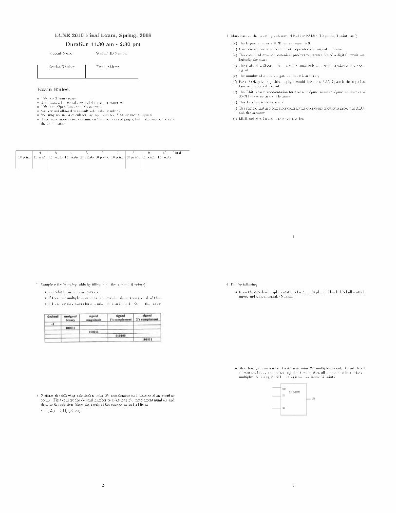
ECSE ���� Final Exam� Spring� ����
Duration ���� am ��� pm
Student Name Student ID Number
Section Number Email Address
Exam Rules�
� This is a � hours exam�� It includes all materials covered during this semester�� This is an Open Book and Notes exam�� You are not allowed to consult with other students�� You may not use a calculator� laptop� palmtop� PDA� or such computer�� If you need more space� continue on the back sides of pages� but make sure to indicatethe continuation�
� � � � � � � � � Total
� points � points � points � points � points � points � points � points � points � points
�� Mark each of the following statement TRUE or FALSE ��� points� � point each�
�a� The largest number a BCD can represent is �
�b� Overow applies only to arithmetic operations on signed numbers�
�c� The canonical sum and canonical product representation of a digital circuit arelogically the same�
�d� The state of a Moore machine will change only at the rising edge of the clocksignal�
�e� The number of outputs a gate can have is arbitrary�
�f� For a NOR gate in positive logic� it would become a NAND gate if the negativelogic were applied instead�
�g� The ��bit binary representation for as a unsigned number� signed number� or aASCII character are all the same�
�h� The data bus is bidirectional�
�i� The control unit in a computer controls the operations of every register� the ALU�and the memory�
�j� MBR and MAR use di�erent types of bus�
�
�� Complete the following table by �lling in all the blanks ��� points�
� use ��bit binary representations
� if there are multiple answers for a particular blank� then give all of them
� if there are no answers for a blank� then mark it with �X� in that space
�� Perform the following calculation using ��s complement and indicate if an overowoccurs� First convert the decimal number to ��bit long ��s complement numbers andthen do the addition� Show the result of the conversion and addition�
z � ����� � ����� ��� pts�
�
�� Do the following
� Draw the gate�level implementation of a ��� multiplexer� Clearly label all control�input� and output signals �� points�
� Show how you can construct a ��� mux using ��� multiplexers only� Clearly labelall control� input� and output signals� Clearly show all the connections betweenmultiplexers� Using the ��� mux logic symbol below �� points��
�

�� Give the state diagram for the logic diagram below� where FA�full adder� Identify theinputs� outputs� and states explicitly ��� points��
� A combinational logic circuit accepts a �bit unsigned number �A�A�A�A�� and gen�erates a binary output �P
nPn��P�P�P�� equal to the eight times the input� Find the
simpli�ed sum of products for P� and P� only ��� points�
�
� An �AB�type� �ip��op has two inputs A and B� If A��� then Q��B� if A��� thenQ��B� ��� points��
� Using a D �ip��op� design an AB �ip��op� Show how you derived the schematicand draw the schematic�
� Using an AB �ip��op� design a T �ip��op� Explain how you derived the schematic�
�� Given the following timing chart for a negatively edge�triggered sequential network�where X� and X� are inputs� Q� and Q� are state variables� and Z� and Z� representtwo outputs� Is this a Moore or Mealy or Moore machine and why � Construct asmuch of the state diagram as possible ��� points��
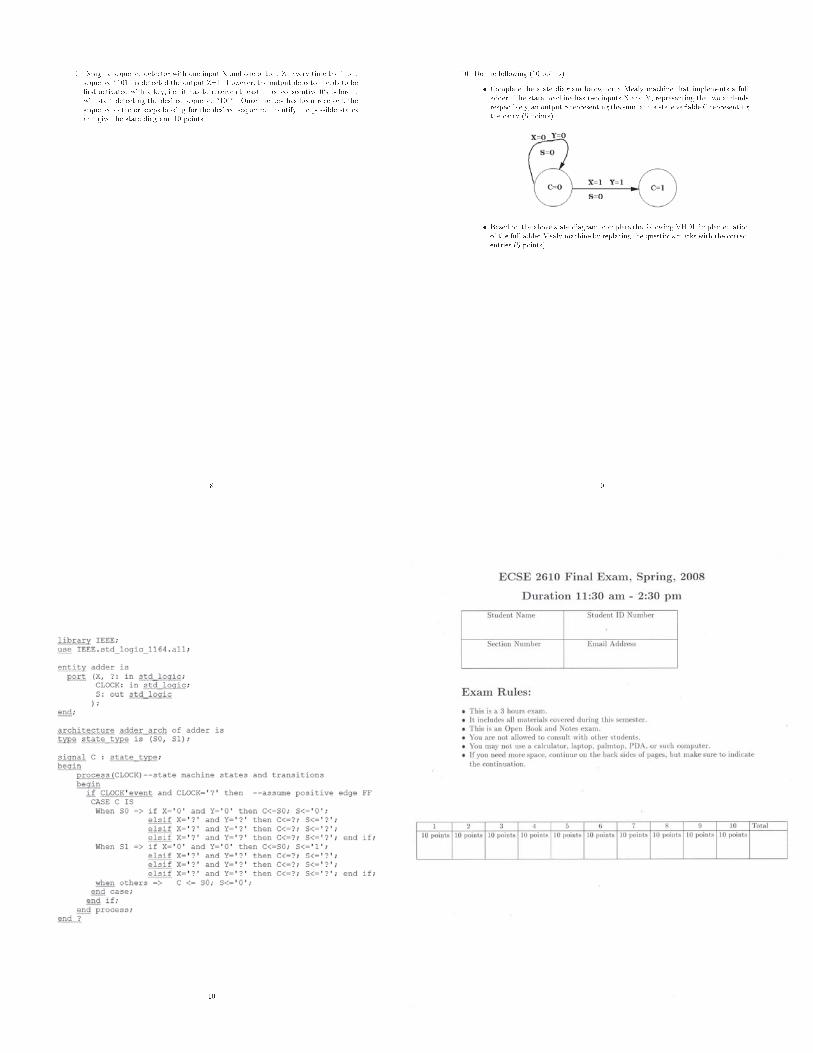
�� Design a sequence detector with one input X and one output Z� Every time the inputsequence ����� is detected the output Z��� However� the output detector needs to be�rst activated with a key� i�e� it has to receive at least three consecutive �s before itwill start detecting the desired sequence ������ Once the key has been received� thesequence detector keeps looking for the desired sequence� Identify the possible statesand give the state diagram �� points��
�
��� Do the following �� points�
� Complete the state diagram below for a Mealy machine that implements a fulladder� The state machine has two inputs X and Y� representing the two addendsrespectively� an output S representing the sum� and a state variable C representingthe carry � points�
� Based on the above state diagram� complete the following VHDL implementationof the full adder Mealy machine by replacing the questions marks with the correctentries � points��
�
��
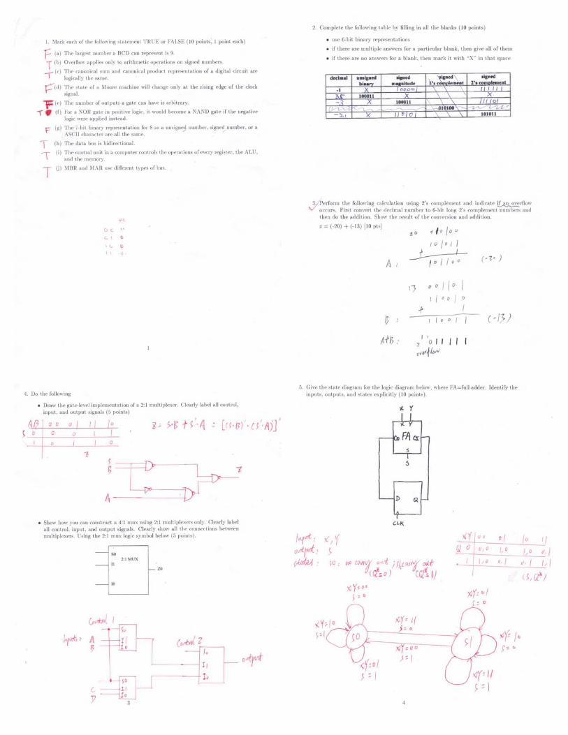
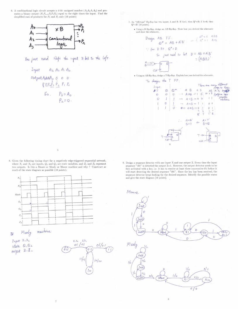
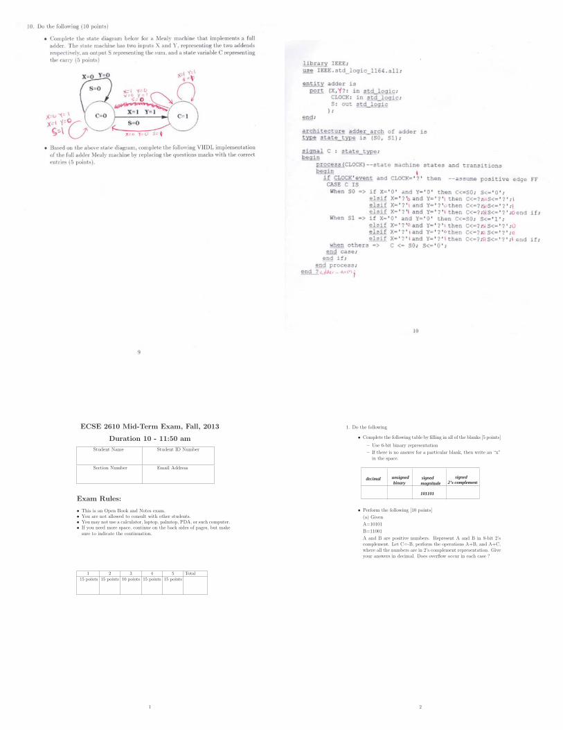
ECSE 2610 Mid-Term Exam, Fall, 2013
Duration 10 - 11:50 am
Student Name Student ID Number
Section Number Email Address
Exam Rules:
• This is an Open Book and Notes exam.
• You are not allowed to consult with other students.
• You may not use a calculator, laptop, palmtop, PDA, or such computer.
• If you need more space, continue on the back sides of pages, but make
sure to indicate the continuation.
1 2 3 4 5 Total
15 points 15 points 10 points 15 points 15 points
1
1. Do the following
• Complete the following table by filling in all of the blanks [5 points]
– Use 6-bit binary representation
– If there is no answer for a particular blank, then write an “x”
in the space.
magnitude 2’s complementsignedsignedunsigned
binarydecimal
101101
• Perform the following [10 points]
(a) Given
A=10101
B=11001
A and B are positive numbers. Represent A and B in 8-bit 2’s
complement. Let C=-B, perform the operations A+B, and A+C,
where all the numbers are in 2’s complement representation. Give
your answers in decimal. Does overflow occur in each case ?
2
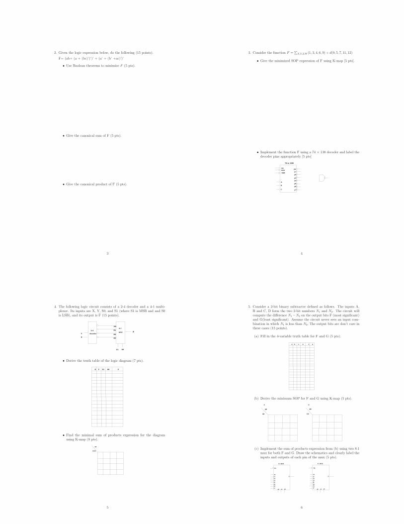
2. Given the logic expression below, do the following (15 points).
F= (ab+ (a + (bc)’)’)’ + (a’ + (b’ +ac)’)’
• Use Boolean theorems to minimize F (5 pts).
• Give the canonical sum of F (5 pts).
• Give the canonical product of F (5 pts).
3
3. Consider the function F =∑
X,Y,Z,W (1, 3, 4, 6, 9) + d(0, 5, 7, 11, 12)
• Give the minimized SOP expression of F using K-map [5 pts].
• Implement the function F using a 74 × 138 decoder and label the
decoder pins appropriately [5 pts]
74 x 138
G1G2A
G2B
C
B
A
y0
y1
y2
y3
y4
y5
y6
y7
4
4. The following logic circuit consists of a 2-4 decoder and a 4-1 multi-
plexer. Its inputs are X, Y, S0, and S1 (where S1 is MSB and and S0
is LSB), and its output is F (15 points).
F
S1 S0
X
Y decoder
2-44-1
mux
D0
D1
D2
D3
• Derive the truth table of the logic diagram (7 pts).
X Y S1 S0 F
• Find the minimal sum of products expression for the diagram
using K-map (8 pts).
XY
S1S0
5
5. Consider a 2-bit binary subtracter defined as follows. The inputs A,
B and C, D form the two 2-bit numbers N1 and N2. The circuit will
compute the difference N1−N2 on the output bits F (most significant)
and G(least significant). Assume the circuit never sees an input com-
bination in which N1 is less than N2, The output bits are don’t care in
these cases (15 points).
(a) Fill in the 4-variable truth table for F and G (5 pts).
A B C D F G
(b) Derive the minimum SOP for F and G using K-map (5 pts).
F G
AB
CDCD
AB
(c) Implement the sum of products expression from (b) using two 8:1
mux for both F and G. Draw the schematics and clearly label the
inputs and outputs of each pin of the mux (5 pts).
8:1 MUX
s1s2 s0
Y
En
I0
I1I2
I3I4
I5I6
I7
8:1 MUX
s1s2 s0
Y
En
I0
I1I2
I3I4
I5I6
I7
6
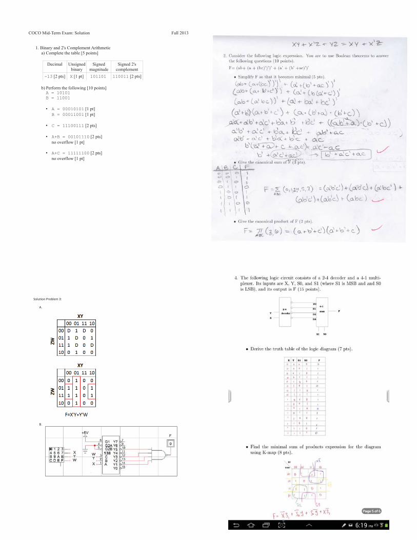
Solution Problem 3:
A.
B.
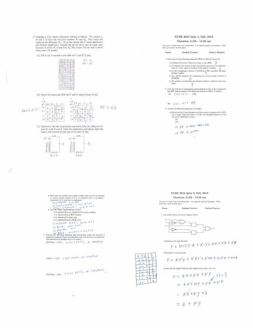
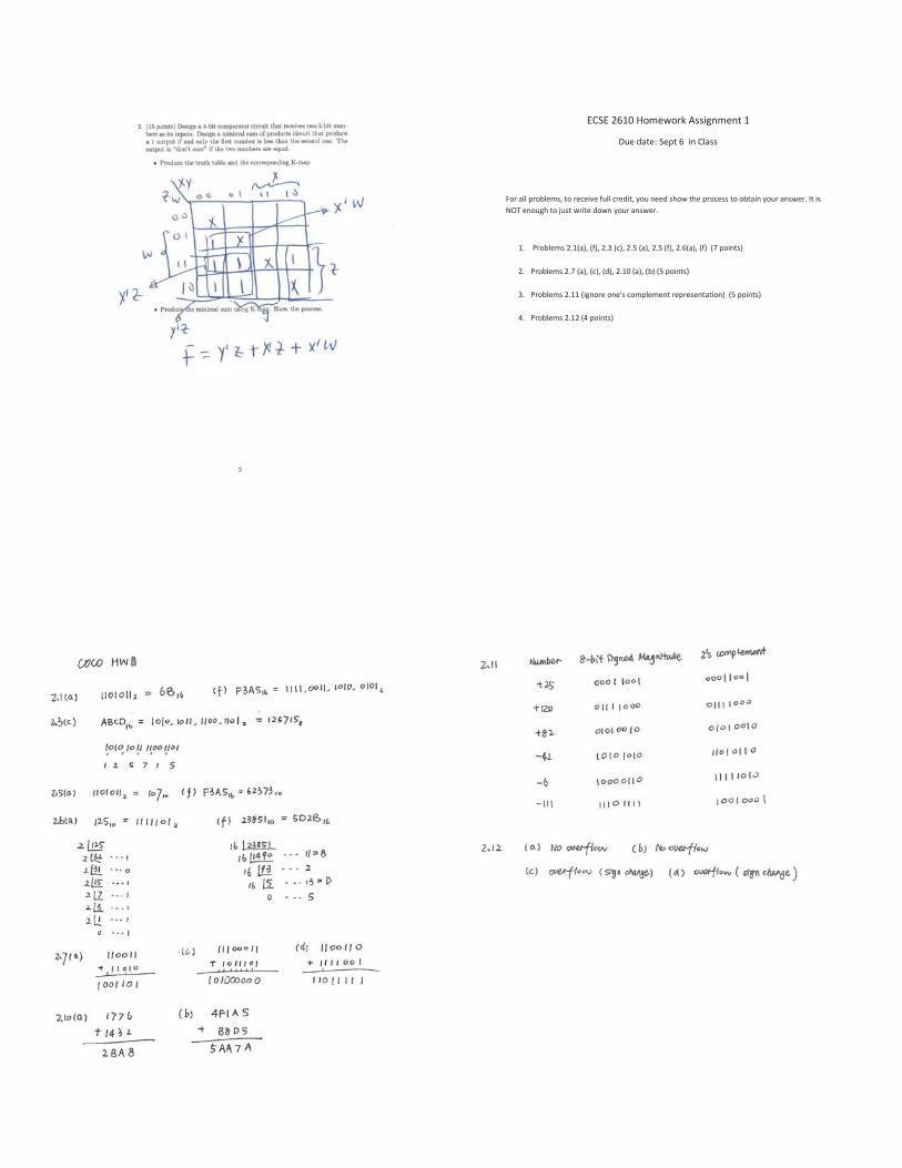
ECSE 2610 Homework Assignment 1
Due date: Sept 6 in Class
For all problems, to receive full credit, you need show the process to obtain your answer. It is NOT enough to just write down your answer.
1. Problems 2.1(a), (f), 2.3 (c), 2.5 (a), 2.5 (f), 2.6(a), (f) (7 points)
2. Problems 2.7 (a), (c), (d), 2.10 (a), (b) (5 points)
3. Problems 2.11 (ignore one's complement representation) (5 points)
4. Problems 2.12 (4 points)
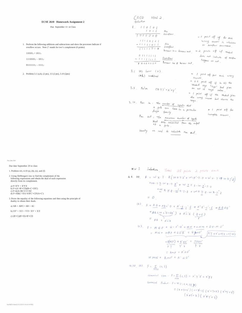
ECSE 2610 Homework Assignment 2
Due September 13 in Class
1. Perform the following additions and subtractions and show the processes Indicate if overflow occurs. Note 2’ stands for two’s complement (6 points)
1101012 + 10112
111101012’ - 10112’
011111112’ - 11112’
2. Problem 3.1 (a,h), (2 pts), 3.5 (2 pts), 3.10 (2pts)
Due date Feb
hw3fall13.htm[12/12/2013 10:43:19 PM]
Due date September 20 in class
1. Problem 4.6, 4.10 (a), (b), (e), and (f)
2. Using DeMorgan's law to find the complement of thefollowing expressions and obtain the dual of each expressiondirectly from its complement.
a) F=X'Y + X'Y'Zb) F=(A'+B'+CD)(B+C'+D'E')c) F=(((A+B)'+C')'+D)'d) F=AB(C'+D')+A'B'C'+CD'(A+C')
3. Prove the equality of the following equations and then using the principle ofduality to obtain their duals.
a) AB + AB'C= AB + AC
b) XY' + X'Z + Y'Z= XY' + X'Z
c) (B'+C)(B'+D)=B'+CD

COCO 2610 Homework 4 due date: Sept. 27 in class
1) 4-14 (c)-(f)2) 4-15 (a) and (f)
3) Given F=X+YZ a) give its truth table b) give its canonical sum c) give its canonical product d) explain the difference between the original expression (F=X+YZ) and the canonical sum
4) Design a combinational circuit that takes 2 inputs andoutputs its two's complement.a) specify the input and output, how many outputs ?b) produce the truth tablec) give the canonical sum for each outputd) minimize each output expression if necessary using K-map
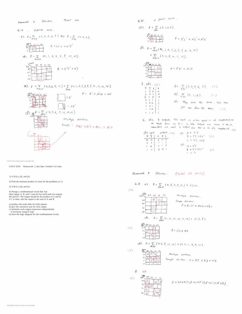
COCO 2610 Homework 5, due date: Feb
HW5Fall13.htm[12/12/2013 10:43:20 PM]
COCO 2610 Homework 5, due date: October 4 in class
1) 4.18 (c), (d), and (e)
2) Find the minimal product of sums for the problems in 1)
3) 4.58 (c), (d), and (e)
4) Design a combinational circuit that hasthree inputs A, B, and C (one bit for each) and two outputsD0 and D1. The output should be the product of A and Bif C is false, else the output is the sum of A and B
a) produce the truth table for both outputsb) give the canonical sum for each outputc) minimize each output expression independently
if necessary using K-mapd) draw the logic diagram for the combinational circuit.
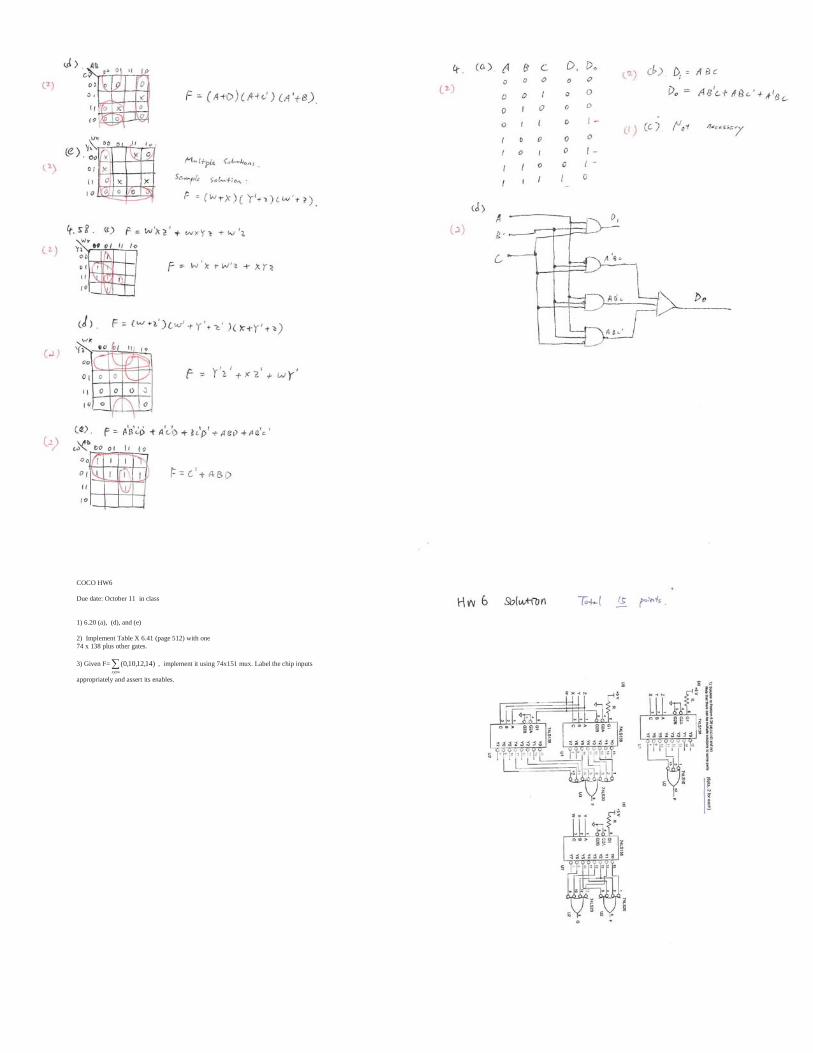
COCO HW6
Due date: October 11 in class
1) 6.20 (a), (d), and (e)
2) Implement Table X 6.41 (page 512) with one74 x 138 plus other gates.
3) Given F=xyzw
)14,12,10,0( , implement it using 74x151 mux. Label the chip inputs
appropriately and assert its enables.
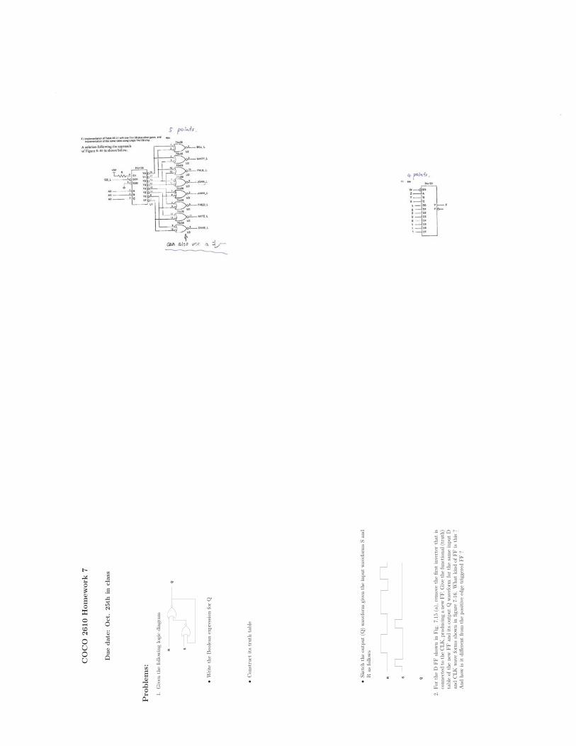
COCO
2610Homework
7
Duedate:Oct.25th
inclass
Pro
blems:
1.Giventhefollowinglogic
diagram
R S
Q
•WritetheBooleanexpressionforQ
•Constructitstruthtable
•Sketchtheoutput(Q)waveform
giventheinputwaveformsSand
Rasfollows
R S Q
2.FortheD
FFshownin
Fig.7.15(a),removethefirstinverterthatis
connectedtotheCLK,producinganewFF.Givethefunctional(truth)
table
ofthenew
FFanditsoutputQ
waveform
forthesameinputD
andCLK
waveformsshownin
figure7-16.W
hatkindofFFis
this
?
Andhow
isitdifferentfrom
thepositiveedgetriggeredFF?
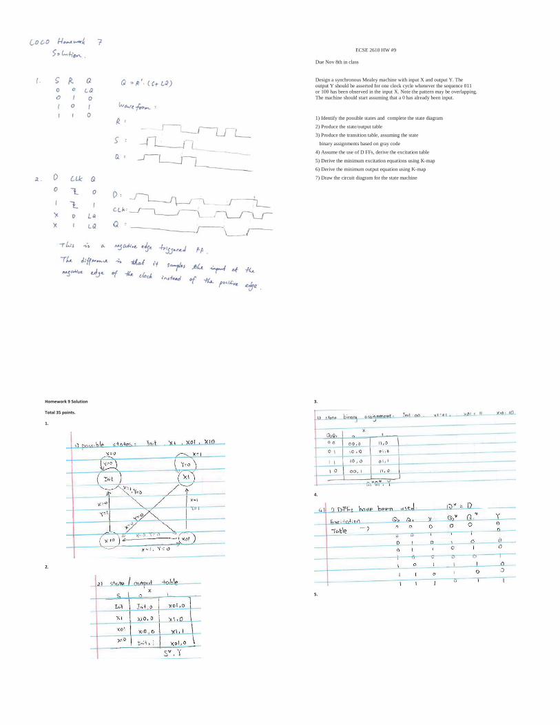
ECSE 2610 HW #9
Due Nov 8th in class
Design a synchronous Mealey machine with input X and output Y. Theoutput Y should be asserted for one clock cycle whenever the sequence 011or 100 has been observed in the input X. Note the pattern may be overlapping.The machine should start assuming that a 0 has already been input.
1) Identify the possible states and complete the state diagram
2) Produce the state/output table3) Produce the transition table, assuming the state
binary assignments based on gray code4) Assume the use of D FFs, derive the excitation table
5) Derive the minimum excitation equations using K-map6) Derive the minimum output equation using K-map
7) Draw the circuit diagram for the state machine
Homework 9 Solution
Total 35 points.
1.
2.
3.
4.
5.
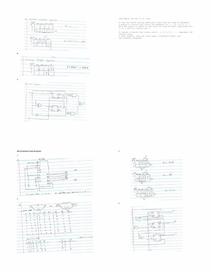
6.
7.
COCO HW#10, Due Nov 15 in class
2) Use the 74x163 and any additional logic that you need to implementa modulo-11 counter that counts the sequence 5,6, .., 15, 15, 5, 6 ...Note RCO output in 74x163 is the carry-out from the most significant bit.It is 1 when all outputs are 1.
3) Design a counter that counts from 0, 1, 3, 5, 0 1, ... Implement the counter usingT (with enable). Show the state table, transition table, andthe schematic diagrams.
HW 10 Solution (Total 20 points)
1.
2.
3.
4.
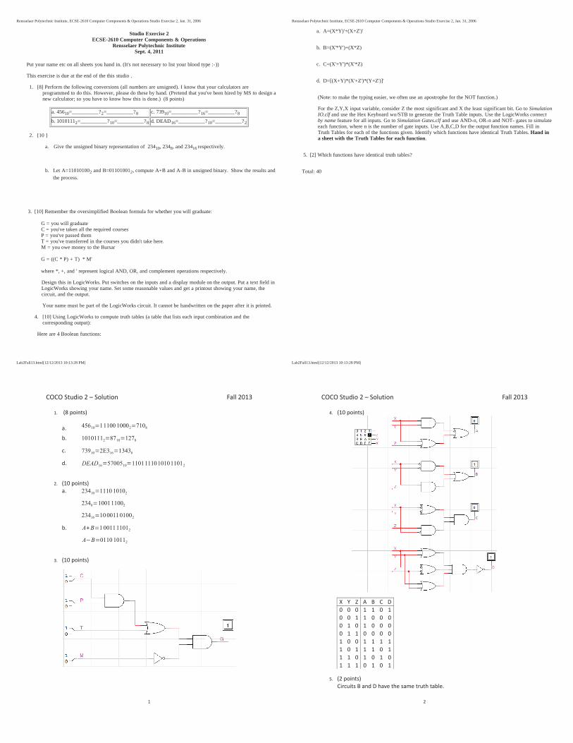
Rensselaer Polytechnic Institute, ECSE-2610 Computer Components & Operations Studio Exercise 2, Jan. 31, 2006
Lab2Fall13.html[12/12/2013 10:13:28 PM]
Studio Exercise 2ECSE-2610 Computer Components & Operations
Rensselaer Polytechnic InstituteSept. 4, 2011
Put your name etc on all sheets you hand in. (It's not necessary to list your blood type :-))
This exercise is due at the end of the this studio .
1. [8] Perform the following conversions (all numbers are unsigned). I know that your calculators areprogrammed to do this. However, please do these by hand. (Pretend that you've been hired by MS to design anew calculator; so you have to know how this is done.) (8 points)
a. 45610=__________?2=__________?8 c. 73910=__________?16=__________?8
b. 10101112=__________?10=__________?8 d. DEAD16=__________?10=__________?2
2. [10 ]
a. Give the unsigned binary representation of 23410, 2348, and 23416 respectively.
b. Let A=110101002 and B=011010012, compute A+B and A-B in unsigned binary. Show the results andthe process.
3. [10] Remember the oversimplified Boolean formula for whether you will graduate:
G = you will graduateC = you've taken all the required coursesP = you've passed themT = you've transferred in the courses you didn't take here.M = you owe money to the Bursar
G = ((C * P) + T) * M'
where *, +, and ' represent logical AND, OR, and complement operations respectively.
Design this in LogicWorks. Put switches on the inputs and a display module on the output. Put a text field inLogicWorks showing your name. Set some reasonable values and get a printout showing your name, thecircuit, and the output.
Your name must be part of the LogicWorks circuit. It cannot be handwritten on the paper after it is printed.
4. [10] Using LogicWorks to compute truth tables (a table that lists each input combination and thecorresponding output):
Here are 4 Boolean functions:
Rensselaer Polytechnic Institute, ECSE-2610 Computer Components & Operations Studio Exercise 2, Jan. 31, 2006
Lab2Fall13.html[12/12/2013 10:13:28 PM]
a. A=(X*Y)'+(X+Z')'
b. B=(X'*Y')+(X*Z)
c. C=(X'+Y')*(X'*Z)
d. D=[(X+Y)*(X'+Z')*(Y+Z')]'
(Note: to make the typing easier, we often use an apostrophe for the NOT function.)
For the Z,Y,X input variable, consider Z the most significant and X the least significant bit. Go to SimulationIO.clf and use the Hex Keyboard wo/STB to generate the Truth Table inputs. Use the LogicWorks connectby name feature for all inputs. Go to Simulation Gates.clf and use AND-n, OR-n and NOT- gates to simulateeach function, where n is the number of gate inputs. Use A,B,C,D for the output function names. Fill inTruth Tables for each of the functions given. Identify which functions have identical Truth Tables. Hand ina sheet with the Truth Tables for each function.
5. [2] Which functions have identical truth tables?
Total: 40
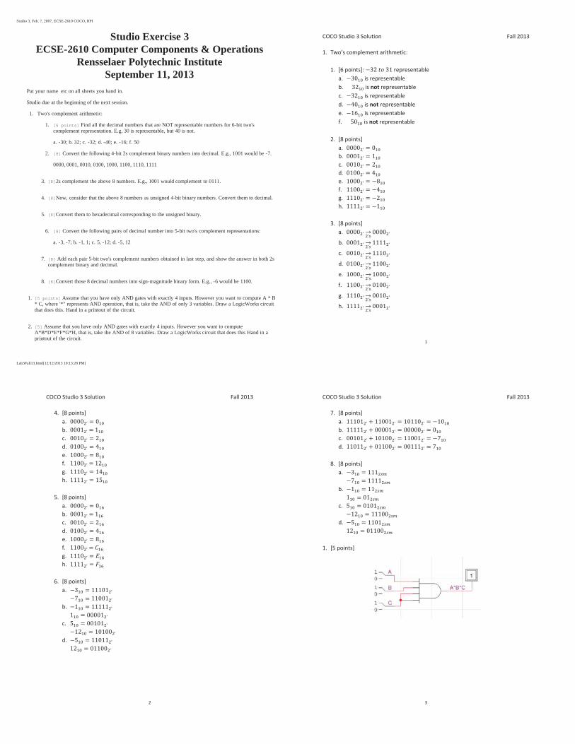
Studio 3, Feb. 7, 2007, ECSE-2610 COCO, RPI
Lab3Fall13.html[12/12/2013 10:13:28 PM]
Studio Exercise 3ECSE-2610 Computer Components & Operations
Rensselaer Polytechnic InstituteSeptember 11, 2013
Put your name etc on all sheets you hand in.
Studio due at the beginning of the next session.
1. Two's complement arithmetic:
1. [6 points] Find all the decimal numbers that are NOT representable numbers for 6-bit two'scomplement representation. E.g, 30 is representable, but 40 is not.
a. -30; b. 32; c. -32; d. -40; e. -16; f. 50
2. [8] Convert the following 4-bit 2s complement binary numbers into decimal. E.g., 1001 would be -7.
0000, 0001, 0010, 0100, 1000, 1100, 1110, 1111
3. [8]2s complement the above 8 numbers. E.g., 1001 would complement to 0111.
4. [8]Now, consider that the above 8 numbers as unsigned 4-bit binary numbers. Convert them to decimal.
5. [8]Convert them to hexadecimal corresponding to the unsigned binary.
6. [8] Convert the following pairs of decimal number into 5-bit two's complement representations:
a. -3, -7; b. -1, 1; c. 5, -12; d. -5, 12
7. [8] Add each pair 5-bit two's complement numbers obtained in last step, and show the answer in both 2scomplement binary and decimal.
8. [8]Convert those 8 decimal numbers into sign-magnitude binary form. E.g., -6 would be 1100.
1. [5 points] Assume that you have only AND gates with exactly 4 inputs. However you want to compute A * B* C, where '*" represents AND operation, that is, take the AND of only 3 variables. Draw a LogicWorks circuitthat does this. Hand in a printout of the circuit.
2. [5] Assume that you have only AND gates with exactly 4 inputs. However you want to computeA*B*D*E*F*G*H, that is, take the AND of 8 variables. Draw a LogicWorks circuit that does this Hand in aprintout of the circuit.
COCO Studio 3 Solution Fall 2013
1
1. Two’s complement arithmetic: 1. [6 points]: representable
a. is representable b. is not representable c. is representable d. is not representable e. is representable f. is not representable
2. [8 points]
a. b. c. d. e. f. g. h.
3. [8 points]
a.
b.
c.
d.
e.
f.
g.
h.
COCO Studio 3 Solution Fall 2013
2
4. [8 points] a. b. c. d. e. f. g. h.
5. [8 points]
a. b. c. d. e. f. g. h.
6. [8 points]
a.
b.
c.
d.
COCO Studio 3 Solution Fall 2013
3
7. [8 points] a. b. c. d.
8. [8 points]
a.
b.
c.
d.
1. [5 points]
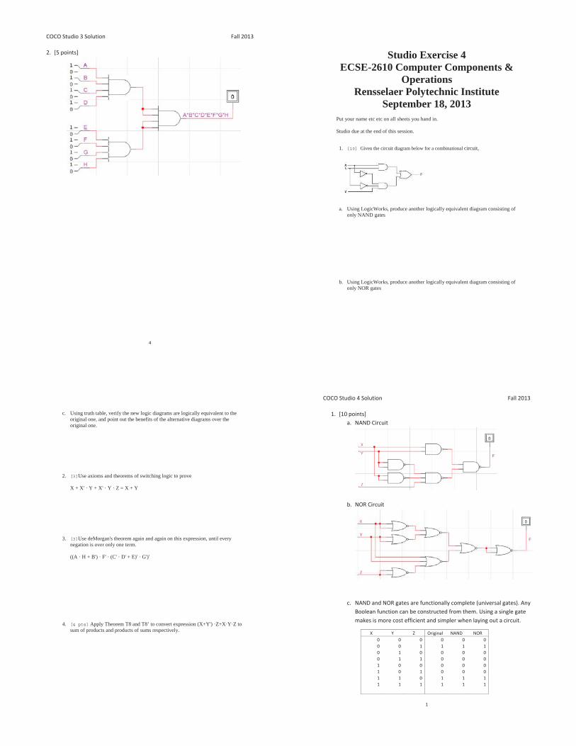
COCO Studio 3 Solution Fall 2013
4
2. [5 points]
Studio Exercise 4 ECSE-2610 Computer Components &
Operations Rensselaer Polytechnic Institute
September 18, 2013 Put your name etc etc on all sheets you hand in.
Studio due at the end of this session.
1. [10] Given the circuit diagram below for a combinational circuit,
a. Using LogicWorks, produce another logically equivalent diagram consisting of only NAND gates
b. Using LogicWorks, produce another logically equivalent diagram consisting of only NOR gates
c. Using truth table, verify the new logic diagrams are logically equivalent to the original one, and point out the benefits of the alternative diagrams over the original one.
2. [3]Use axioms and theorems of switching logic to prove
X + X' · Y + X' · Y · Z = X + Y
3. [3]Use deMorgan's theorem again and again on this expression, until every negation is over only one term.
((A · H + B') · F' · (C' · D' + E)' · G')'
4. [4 pts] Apply Theorem T8 and T8’ to convert expression (X+Y') ·Z+X·Y·Z to sum of products and products of sums respectively.
COCO Studio 4 Solution Fall 2013
1
1. [10 points] a. NAND Circuit
b. NOR Circuit
c. NAND and NOR gates are functionally complete (universal gates). Any
Boolean function can be constructed from them. Using a single gate makes is more cost efficient and simpler when laying out a circuit.
X Y Z Original NAND NOR 0 0 0 0 0 0 0 0 1 1 1 1 0 1 0 0 0 0 0 1 1 0 0 0 1 0 0 0 0 0 1 0 1 0 0 0 1 1 0 1 1 1 1 1 1 1 1 1
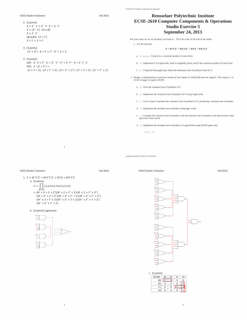
COCO Studio 4 Solution Fall 2013
2
2. [3 points]
3. [3 points]
4. [4 points] SOP: POS:
ECSE-2610 Computer Components & Operations
Lab5Fall13.html[12/12/2013 10:13:28 PM]
Rensselaer Polytechnic InstituteECSE-2610 Computer Components & Operations
Studio Exercise 5September 24, 2013
Put your name etc etc on all sheets you hand in. The Lab is due at the end of the studio
1. For the function
F = W'Y'Z' + WX'YZ' + WYZ + WX'Y'Z
a. [5 points] Convert to a canonical product of sums form.
b. [5] Implement F in Logicworks, both as originally given, and in the canonical product of sums form.
c. [5] Using the Karnaugh map, obtain the minimum sum of products form for F.
1. Design a combinational circuit that consists of four inputs A1,A0,B1,B0 and one output F. The output is 1 ifA1A0 is larger or equal to B1B0.
a. [5] Give the canonical sum of products of F
b. [5] Implement the canonical sum of products of F using Logicworks
c. [7] Use K-map to minimize the canonical sum of products of F, producing a minimal sum of product
d. [5] Implement the minimal sum of product using logic works
e. [3] Compare the canonical sum of products with the minimal sum of products and find out how manygates have been saved.
f. [5] Implement the minimal sum of products in LogicWorks using NAND gates only.
Total: 45
COCO Studio 5 Solution Fall 2013
1
1. a. [5 points]
b. [5 points] Logicworks
W
W
W
W
X
X
Y
Y
Y
Y
Z
Z
Z
Z
F
COCO Studio 5 Solution Fall 2013
2
c. [5 points] YZ\WX 00 01 11 10
00 1 1 0 0 01 0 0 0 1 11 0 0 1 1 10 0 0 0 1
W
W
W
W
W
W
X
X
X
X
Y
Y
Y
Y
Y
Z'
Z'
Z'
Z'
Z'
W'
W'
W'
W'
X'
X'
X'
X'
X'
Y'
Y'
Y'
Y'
Y'
Y'
Z
Z
Z
Z
Z
F
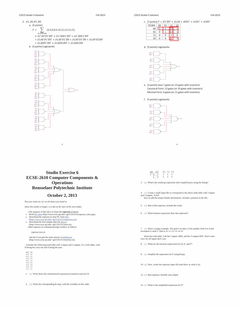
COCO Studio 5 Solution Fall 2013
3
2. a. [5 points]
b. [5 points] Logicworks
A1'
A1'
A1'
A0'
A0'
A0'
A0'
B1
B1
B1
B0
B0
B0
A0
A0
A0
A0
A0
A0
B1'
B1'
B1'
B1'
B1'
B1'
B1'
A1
A1
A1
A1
A1
A1
A1
B0'
B0'
B0'
B0'
B0'
B0'
B0'
F
COCO Studio 5 Solution Fall 2013
4
c. [7 points] YZ\WX 00 01 11 10
00 1 1 1 1 01 0 1 1 1 11 0 0 1 0 10 0 0 1 1
d. [5 points] Logicworks
e. [3 points] Save 7 gates (or 22 gates with inverters)
Canonical Form: 13 gates (or 33 gates with inverters) Minimal Form: 6 gates (or 11 gates with inverters)
f. [5 points] Logicworks
A0
A0
B1'
B1'
B1'
A1
A1
A1
B0'
B0'
F
A0
A0
B1'
B1'
B1'
A1
A1
A1
B0'
B0'
F
Studio Exercise 6 ECSE-2610 Computer Components &
Operations Rensselaer Polytechnic Institute
October 2, 2013 Put your name etc etc on all sheets you hand in.
Since this studio is longer, it is due at the start of the next studio.
• The purpose of this lab is to learn the espresso program. • Read this intro (http://www.ecse.rpi.edu/~qji/COCO13/espresso_intro.ppt). • Download the espresso to your PC from here
(http://www.ecse.rpi.edu/~qji/COCO13/espresso.exe) • Download the first sample data file test.txt
(http://www.ecse.rpi.edu/~qji/COCO13/test.txt). • Run espresso in command prompt window as follows
espresso test.txt
and see if you get the same answer as testOut.txt(http://www.ecse.rpi.edu/~qji/COCO13/testOut.txt).
Consider the following truth table with 3 inputs and 2 outputs. It’s a full adder, with D being the carry out and S being the sum.
ABC DS 000 00 001 01 010 01 011 10 100 01 101 10 110 10 111 11
1. [5] Write down the unminimized expression (canonical sum) for D.
2. [2] Write the corresponding K-map, with the variables in this order.
3. [2] What's the resulting expression after simplification using the Kmap?
4. [2] Create a small input file to correspond to the above truth table with 3 inputs and 2 outputs. You'll have to add the proper header declarations. Include a printout of the file.
5. [2] Run it thru espresso; include the result.
6. [2] What boolean expression does that represent?
7. [2] Here's a larger example. The goal is to take a 3-bit number from 0 to 4 and increment it, mod 5. That is, 0->1->2->3->4->0.
Write the truth table. Call the 3 inputs ABD, and the 3 outputs DEF. Don't write rows for all inputs don't care.
8. [3] What are the boolean expressions for D, E, and F?
9. [2] Simplify the espression for F using Kmap.
10. [2] Now, create the espresso input file (and show us what it is).
11. [2] Run espresso. Include your output.
12. [1] What is the simplified expression for F?
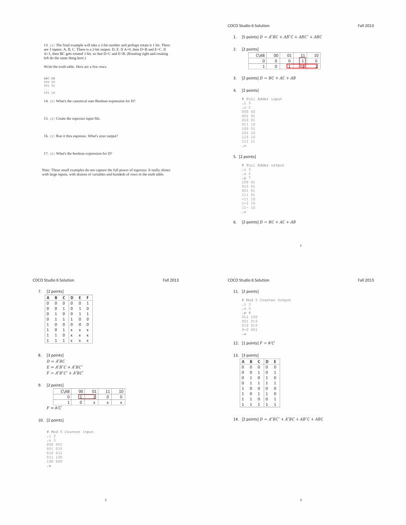
13. [3] The final example will take a 2-bit number and perhaps rotate it 1 bit. There are 3 inputs: A, B, C. There is a 2-bit output: D, E. If A=0, then D=B and E=C. If A=1, then BC gets rotated 1 bit, so that D=C and E=B. (Rotating right and rotating left do the same thing here.)
Write the truth table. Here are a few rows.
ABC DE 000 00 001 01 ... 101 10
14. [2] What's the canonical sum Boolean expression for D?
15. [2] Create the espresso input file.
16. [2] Run it thru espresso. What's your output?
17. [2] What's the boolean expression for D?
Note: These small examples do not capture the full power of espresso. It really shines with large inputs, with dozens of variables and hundeds of rows in the truth table.
COCO Studio 6 Solution Fall 2013
1
1. [5 points]
2. [2 points] C\AB 00 01 11 10
0 0 0 1 0 1 0 1 1 1
3. [2 points]
4. [2 points]
# Full Adder input .i 3 .o 2 000 00 001 01 010 01 011 10 100 01 101 10 110 10 111 11 .e
5. [2 points]
# Full Adder output .i 3 .o 2 .p 7 100 01 010 01 001 01 111 01 -11 10 1-1 10 11- 10 .e
6. [2 points]
COCO Studio 6 Solution Fall 2013
2
7. [2 points] A B C D E F 0 0 0 0 0 1 0 0 1 0 1 0 0 1 0 0 1 1 0 1 1 1 0 0 1 0 0 0 0 0 1 0 1 x x x 1 1 0 x x x 1 1 1 x x x
8. [3 points]
9. [2 points]
C\AB 00 01 11 10 0 1 1 0 0 1 0 x x x
A’C’
10. [2 points] # Mod 5 Counter Input .i 3 .o 3 000 001 001 010 010 011 011 100 100 000 .e
COCO Studio 6 Solution Fall 2013
3
11. [2 points]
# Mod 5 Counter Output .i 3 .o 3 .p 4 011 100 001 010 010 010 0-0 001 .e
12. [1 points] A’C’
13. [3 points] A B C D E 0 0 0 0 0 0 0 1 0 1 0 1 0 1 0 0 1 1 1 1 1 0 0 0 0 1 0 1 1 0 1 1 0 0 1 1 1 1 1 1
14. [2 points]
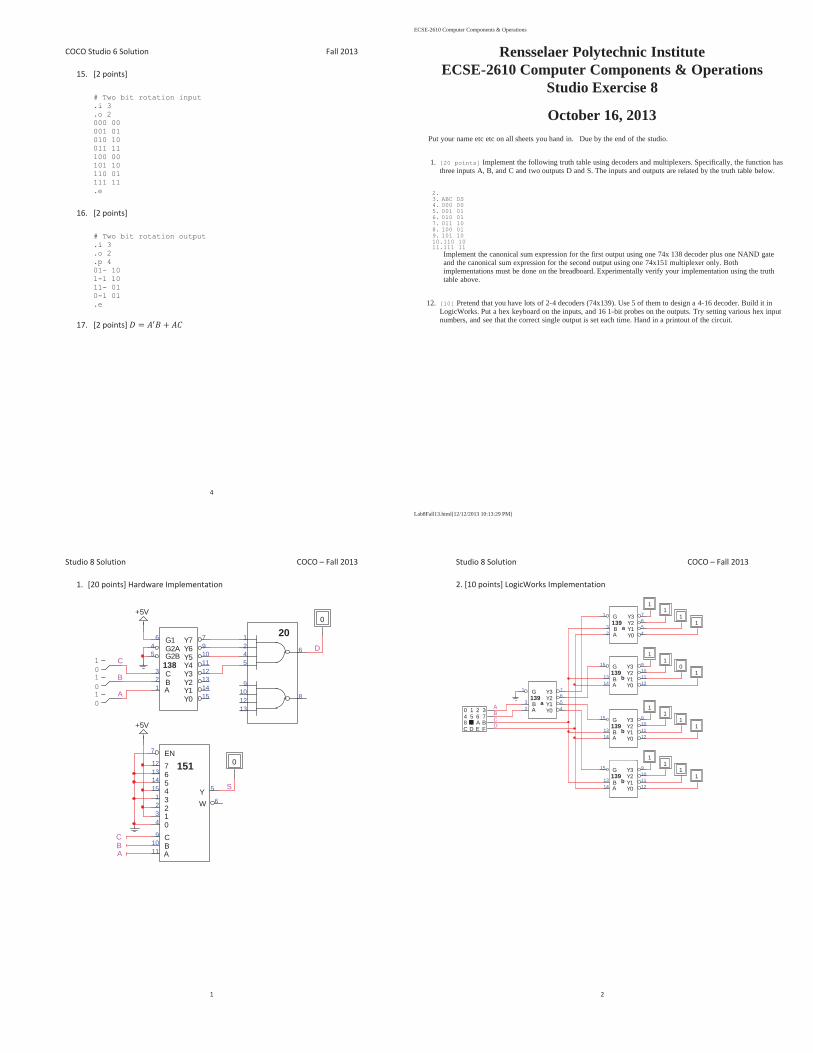
COCO Studio 6 Solution Fall 2013
4
15. [2 points] # Two bit rotation input .i 3 .o 2 000 00 001 01 010 10 011 11 100 00 101 10 110 01 111 11 .e
16. [2 points] # Two bit rotation output .i 3 .o 2 .p 4 01- 10 1-1 10 11- 01 0-1 01 .e
17. [2 points]
ECSE-2610 Computer Components & Operations
Lab8Fall13.html[12/12/2013 10:13:29 PM]
Rensselaer Polytechnic InstituteECSE-2610 Computer Components & Operations
Studio Exercise 8
October 16, 2013Put your name etc etc on all sheets you hand in. Due by the end of the studio.
1. [20 points] Implement the following truth table using decoders and multiplexers. Specifically, the function hasthree inputs A, B, and C and two outputs D and S. The inputs and outputs are related by the truth table below.
2.3. ABC DS4. 000 005. 001 016. 010 017. 011 108. 100 019. 101 1010.110 1011.111 11
Implement the canonical sum expression for the first output using one 74x 138 decoder plus one NAND gateand the canonical sum expression for the second output using one 74x151 multiplexer only. Bothimplementations must be done on the breadboard. Experimentally verify your implementation using the truthtable above.
12. [10] Pretend that you have lots of 2-4 decoders (74x139). Use 5 of them to design a 4-16 decoder. Build it inLogicWorks. Put a hex keyboard on the inputs, and 16 1-bit probes on the outputs. Try setting various hex inputnumbers, and see that the correct single output is set each time. Hand in a printout of the circuit.
Studio 8 Solution COCO – Fall 2013
1
1. [20 points] Hardware Implementation
01
01
01
0
G1G2AG2B
CBA
Y7Y6Y5Y4
Y1Y0
Y3Y2
138
6
12111097
45
321
151413
201
9
2
10
4
12
5
13
6
8
+5V
EN
76543210
CBA
151
WY
7
4321
15141312
11109
6
5
0
+5V
D
A
A
B
B
C
C
S
Studio 8 Solution COCO – Fall 2013
2
2. [10 points] LogicWorks Implementation
G
BA
Y1Y0
Y3Y2139
a23
1
4567
G
BA
Y1Y0
Y3Y2139
a23
1
4567
G
BA
Y1Y0
Y3Y2139
b1413
15
1211109
G
BA
Y1Y0
Y3Y2139
b1413
15
1211109
G
BA
Y1Y0
Y3Y2139
b1413
15
1211109
0 1 2 34 5 6 78 9 A BC D E F
11
11
11
01
11
11
11
11
BA
CD
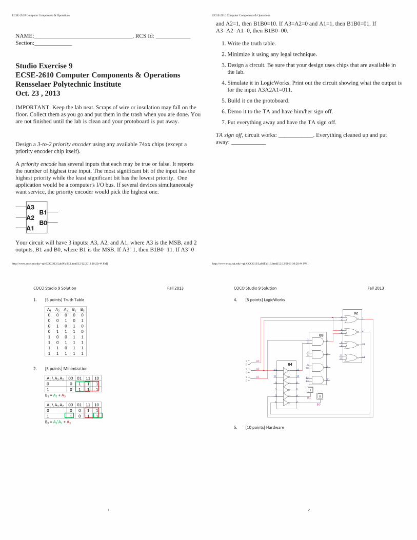
ECSE-2610 Computer Components & Operations
http://www.ecse.rpi.edu/~qji/COCO13/Lab9Fall13.html[12/12/2013 10:20:44 PM]
NAME:__________________________________, RCS Id: ____________Section:_____________
Studio Exercise 9ECSE-2610 Computer Components & OperationsRensselaer Polytechnic InstituteOct. 23 , 2013
IMPORTANT: Keep the lab neat. Scraps of wire or insulation may fall on thefloor. Collect them as you go and put them in the trash when you are done. Youare not finished until the lab is clean and your protoboard is put away.
Design a 3-to-2 priority encoder using any available 74xx chips (except apriority encoder chip itself).
A priority encode has several inputs that each may be true or false. It reportsthe number of highest true input. The most significant bit of the input has thehighest priority while the least significant bit has the lowest priority. Oneapplication would be a computer's I/O bus. If several devices simultaneouslywant service, the priority encoder would pick the highest one.
Your circuit will have 3 inputs: A3, A2, and A1, where A3 is the MSB, and 2outputs, B1 and B0, where B1 is the MSB. If A3=1, then B1B0=11. If A3=0
ECSE-2610 Computer Components & Operations
http://www.ecse.rpi.edu/~qji/COCO13/Lab9Fall13.html[12/12/2013 10:20:44 PM]
and A2=1, then B1B0=10. If A3=A2=0 and A1=1, then B1B0=01. IfA3=A2=A1=0, then B1B0=00.
1. Write the truth table.
2. Minimize it using any legal technique.
3. Design a circuit. Be sure that your design uses chips that are available inthe lab.
4. Simulate it in LogicWorks. Print out the circuit showing what the output isfor the input A3A2A1=011.
5. Build it on the protoboard.
6. Demo it to the TA and have him/her sign off.
7. Put everything away and have the TA sign off.
TA sign off, circuit works: ____________. Everything cleaned up and putaway: ____________
COCO Studio 9 Solution Fall 2013
1
1. [5 points] Truth Table
A3 A2 A1 B1 B0
0 0 0 0 0 0 0 1 0 1 0 1 0 1 0 0 1 1 1 0 1 0 0 1 1 1 0 1 1 1 1 1 0 1 1 1 1 1 1 1
2. [5 points] Minimization
A1 \ A3 A2 00 01 11 10 0 0 1 1 1 1 0 1 1 1
B1 = A2 + A3
A1 \ A3 A2 00 01 11 10 0 0 0 1 1 1 1 0 1 1
B0 = A2’A1 + A3
COCO Studio 9 Solution Fall 2013
2
4. [5 points] LogicWorks
5. [10 points] Hardware
081
4
9
12
2
5
10
13
3
6
8
11
04
1
3
5
9
11
13
2
4
6
8
10
12
022
5
8
11
3
6
9
12
1
4
10
13
01
01
01
1
0
A1
B0
B1
A3
A2

Lab 9, S05, ECSE-2610 Computer Components & Operations, RPI
http://www.ecse.rpi.edu/~qji/COCO13/Lab10Fall13.html[12/12/2013 10:21:19 PM]
NAME:__________________________________, RCS Id: ____________Section:_____________
Studio Exercise 11ECSE-2610 Computer Components & OperationsRensselaer Polytechnic InstituteOctober 30, 2013
IMPORTANT: Keep the lab neat. Scraps of wire or insulation may fall on thefloor. Collect them as you go and put them in the trash when you are done. Youare not finished until the lab is clean and your protoboard is put away.
You have until the start of next studio to hand this in.
Consider a new (non-existent) type of flip-flop, the U-V F/F.Here is the Next State Table. (The next state, Q*, is a functionof 3 variables: the current state and the 2 F/F inputs.)
U V Q Q*
0 0 0 0
0 0 1 0
0 1 0 1
0 1 1 0
1 0 0 0
Lab 9, S05, ECSE-2610 Computer Components & Operations, RPI
http://www.ecse.rpi.edu/~qji/COCO13/Lab10Fall13.html[12/12/2013 10:21:19 PM]
1 0 1 1
1 1 0 1
1 1 1 1
Part 1 (3 points)
Write its Excitation Table. (This shows what the 2 inputshave to be to make the F/F change from one particular stateto another particular state.) Use 'x' for don't care. I filled inthe first row.
Q Q* U V
0 0 x 0
0 1
1 0
1 1
Part 2 (4 points)
Use a K-map to find its Characteristic Equation (a Boolean function giving thenext state Q* from the current state Q and inputs U and V).
Lab 9, S05, ECSE-2610 Computer Components & Operations, RPI
http://www.ecse.rpi.edu/~qji/COCO13/Lab10Fall13.html[12/12/2013 10:21:19 PM]
UV
Q 00 01 11 10
0
1
Q* = __________________________________________
Part 3 (7 points)
Your boss wants you to use a U-V F/F. Since it doesn't exist, you'll have tocreate one from a J-K F/F.
So, design the input (excitation) network to make the U-V flip-flop from a J-Kflip-flop.
That is, you'll design a box with inputs U and V, and outputs Q and not Q. Itwill act like a U-V F/F. Inside will be a J-K F/F and some combinational logicproviding inputs to J and K.
This will take some serious thinking:
You know how Q should change depending on U and V (that's the U-V
Lab 9, S05, ECSE-2610 Computer Components & Operations, RPI
http://www.ecse.rpi.edu/~qji/COCO13/Lab10Fall13.html[12/12/2013 10:21:19 PM]
F/F next state table.)
The J-K excitation table tells you what J and K have to be to change Q that way.Write down that table to remind yourself. Hint: construct the J-K excitation tablebased on the J-K characteristic equation the same way as you did for part 1.
Q Q* J K
0 0
0 1
1 0
1 1
Now combine the U-V next state table with the J-K excitation table, tofind what J and K have to be for each value of U and V. I filled in 2 rows.
U V Q Q* J K
0 0 0 0 0 x
0 0 1 0
0 1 0 1
0 1 1 0
1 0 0 0
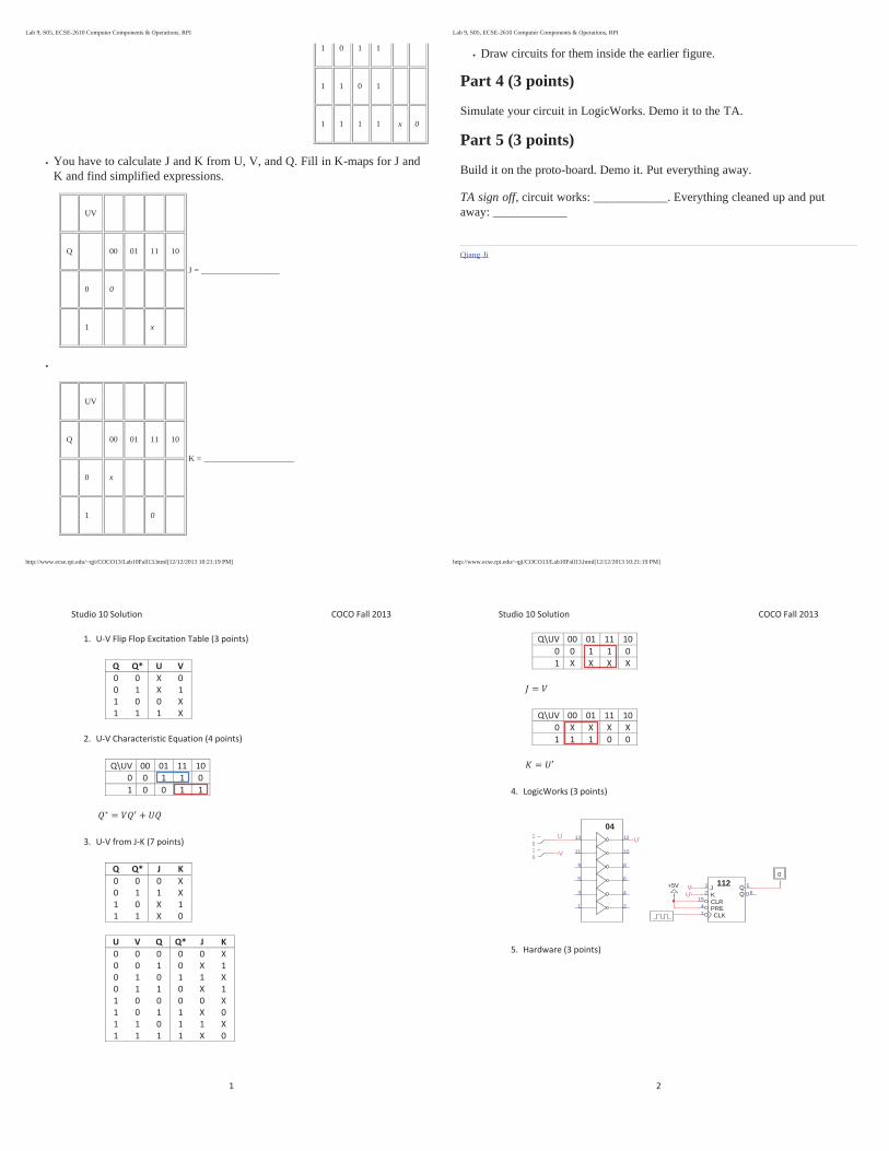
Lab 9, S05, ECSE-2610 Computer Components & Operations, RPI
http://www.ecse.rpi.edu/~qji/COCO13/Lab10Fall13.html[12/12/2013 10:21:19 PM]
1 0 1 1
1 1 0 1
1 1 1 1 x 0
You have to calculate J and K from U, V, and Q. Fill in K-maps for J andK and find simplified expressions.
UV
Q 00 01 11 10
0 0
1 x
J = ___________________
UV
Q 00 01 11 10
0 x
1 0
K = ______________________
Lab 9, S05, ECSE-2610 Computer Components & Operations, RPI
http://www.ecse.rpi.edu/~qji/COCO13/Lab10Fall13.html[12/12/2013 10:21:19 PM]
Draw circuits for them inside the earlier figure.
Part 4 (3 points)
Simulate your circuit in LogicWorks. Demo it to the TA.
Part 5 (3 points)
Build it on the proto-board. Demo it. Put everything away.
TA sign off, circuit works: ____________. Everything cleaned up and putaway: ____________
Qiang Ji
Studio 10 Solution COCO Fall 2013
1
1. U-V Flip Flop Excitation Table (3 points)
Q Q* U V 0 0 X 0 0 1 X 1 1 0 0 X 1 1 1 X
2. U-V Characteristic Equation (4 points)
Q\UV 00 01 11 10
0 0 1 1 0 1 0 0 1 1
3. U-V from J-K (7 points)
Q Q* J K 0 0 0 X 0 1 1 X 1 0 X 1 1 1 X 0
U V Q Q* J K 0 0 0 0 0 X 0 0 1 0 X 1 0 1 0 1 1 X 0 1 1 0 X 1 1 0 0 0 0 X 1 0 1 1 X 0 1 1 0 1 1 X 1 1 1 1 X 0
Studio 10 Solution COCO Fall 2013
2
Q\UV 00 01 11 10 0 0 1 1 0 1 X X X X
Q\UV 00 01 11 10 0 X X X X 1 1 1 0 0
4. LogicWorks (3 points)
5. Hardware (3 points)
CLRK
CLK
J112 Q
Q
PRE1
15
32
4
56
0
04
1
3
5
9
11
13
2
4
6
8
10
12
+5V
01
01
U'
U'
V
V
U
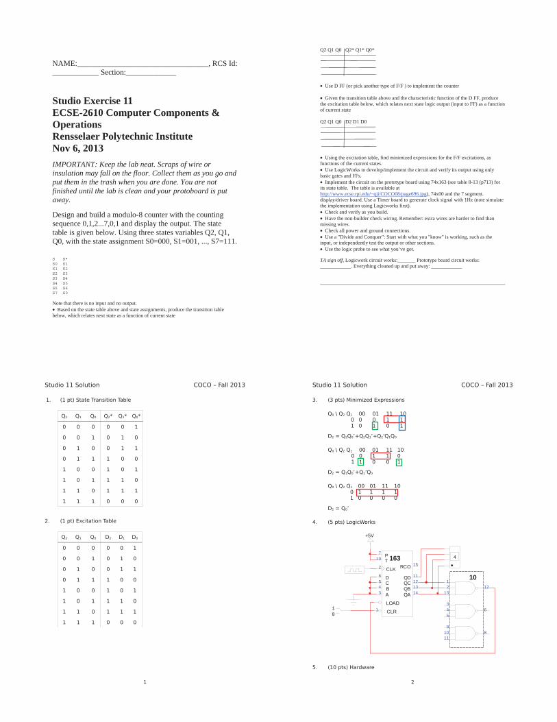
NAME:__________________________________, RCS Id: ____________ Section:_____________
Studio Exercise 11 ECSE-2610 Computer Components & Operations Rensselaer Polytechnic Institute Nov 6, 2013 IMPORTANT: Keep the lab neat. Scraps of wire or insulation may fall on the floor. Collect them as you go and put them in the trash when you are done. You are not finished until the lab is clean and your protoboard is put away.
Design and build a modulo-8 counter with the counting sequence 0,1,2...7,0,1 and display the output. The state table is given below. Using three states variables Q2, Q1, Q0, with the state assignment S0=000, S1=001, ..., S7=111.
S S* S0 S1 S1 S2 S2 S3 S3 S4 S4 S5 S5 S6 S7 S0
Note that there is no input and no output. • Based on the state table above and state assignments, produce the transition table below, which relates next state as a function of current state
Q2 Q1 Q0 Q2* Q1* Q0*
• Use D FF (or pick another type of F/F ) to implement the counter
• Given the transition table above and the characteristic function of the D FF, produce the excitation table below, which relates next state logic output (input to FF) as a function of current state
Q2 Q1 Q0 D2 D1 D0
• Using the excitation table, find minimized expressions for the F/F excitations, as functions of the current states. • Use LogicWorks to develop/implement the circuit and verify its output using only basic gates and FFs. • Implement the circuit on the prototype board using 74x163 (see table 8-13 (p713) for its state table. The table is available at http://www.ecse.rpi.edu/~qji/COCO08/page696.jpg), 74x00 and the 7 segment. display/driver board. Use a Timer board to generate clock signal with 1Hz (note simulate the implementation using Logicworks first). • Check and verify as you build. • Have the non-builder check wiring. Remember: extra wires are harder to find than missing wires. • Check all power and ground connections. • Use a "Divide and Conquer": Start with what you "know" is working, such as the input, or independently test the output or other sections. • Use the logic probe to see what you’ve got.
TA sign off, Logicwork circuit works:_______ Prototype board circuit works: ____________. Everything cleaned up and put away: ____________